EP1432193A1 - Integrierte Modem Schaltung mit softwareimplementation eines PLL Filter - Google Patents
Integrierte Modem Schaltung mit softwareimplementation eines PLL Filter Download PDFInfo
- Publication number
- EP1432193A1 EP1432193A1 EP02293129A EP02293129A EP1432193A1 EP 1432193 A1 EP1432193 A1 EP 1432193A1 EP 02293129 A EP02293129 A EP 02293129A EP 02293129 A EP02293129 A EP 02293129A EP 1432193 A1 EP1432193 A1 EP 1432193A1
- Authority
- EP
- European Patent Office
- Prior art keywords
- modem circuit
- software
- processor
- hardware
- phase locked
- Prior art date
- Legal status (The legal status is an assumption and is not a legal conclusion. Google has not performed a legal analysis and makes no representation as to the accuracy of the status listed.)
- Withdrawn
Links
Images

Classifications
-
- H—ELECTRICITY
- H04—ELECTRIC COMMUNICATION TECHNIQUE
- H04L—TRANSMISSION OF DIGITAL INFORMATION, e.g. TELEGRAPHIC COMMUNICATION
- H04L27/00—Modulated-carrier systems
- H04L27/26—Systems using multi-frequency codes
- H04L27/2601—Multicarrier modulation systems
-
- H—ELECTRICITY
- H04—ELECTRIC COMMUNICATION TECHNIQUE
- H04L—TRANSMISSION OF DIGITAL INFORMATION, e.g. TELEGRAPHIC COMMUNICATION
- H04L7/00—Arrangements for synchronising receiver with transmitter
- H04L7/02—Speed or phase control by the received code signals, the signals containing no special synchronisation information
- H04L7/033—Speed or phase control by the received code signals, the signals containing no special synchronisation information using the transitions of the received signal to control the phase of the synchronising-signal-generating means, e.g. using a phase-locked loop
- H04L7/0331—Speed or phase control by the received code signals, the signals containing no special synchronisation information using the transitions of the received signal to control the phase of the synchronising-signal-generating means, e.g. using a phase-locked loop with a digital phase-locked loop [PLL] processing binary samples, e.g. add/subtract logic for correction of receiver clock
-
- H—ELECTRICITY
- H04—ELECTRIC COMMUNICATION TECHNIQUE
- H04J—MULTIPLEX COMMUNICATION
- H04J3/00—Time-division multiplex systems
- H04J3/02—Details
- H04J3/06—Synchronising arrangements
- H04J3/062—Synchronisation of signals having the same nominal but fluctuating bit rates, e.g. using buffers
- H04J3/0632—Synchronisation of packets and cells, e.g. transmission of voice via a packet network, circuit emulation service [CES]
Definitions
- the invention relates to an integrated modem circuit comprising a processor-system and hardware for exchanging signals with another modem circuit, which integrated modem circuit comprises a digital phase locked loop filter.
- Such an integrated modem circuit corresponds for example with an Asymmetric Digital Subscriber Line modem or ADSL modem or with a Very high speed Digital Subscriber Line modem or VDSL modem etc.
- Said digital phase locked loop filter synchronizes a modem signal (a signal received from said other modem circuit or a signal to be transmitted to said other modem circuit) with an oscillation signal by comparing both signals with each other and generating an error signal etc.
- a prior art modem circuit is known from US 5,790,594, which discloses a modem circuit designed to operate at 2400 to 28800 bit/s and which comprises for example a hardware phase locked loop for the transmitting path and a software phase locked loop for the receiving path (see its figure 6).
- the known integrated modem circuit is disadvantageous, inter alia, due to operating at a low speed.
- the integrated modem circuit according to the invention is characterized in that said integrated modem circuit exchanges signals with another modem circuit at 1 Mb/s or more, with said processor-system comprising filter software for embodying said digital phase locked loop filter and with said hardware comprising at least one module for compensating for sample processing.
- an integrated modem circuit has been created which can operate at 1 Mb/s or more.
- Said filter software is low cost and more accurate (necessary at high speeds) compared to a hardware phase locked loop filter and offers more flexibility.
- Said hardware module can compensate (adapt signals) at higher speeds compared to software phase locked loops.
- modems are able to negotiate with each other the speed to be used. Therefore, the speed of 1 Mb/s or more corresponds with the maximum or theoretical modem speed, during operation, for example in case of a low quality connection between both modems, lower speeds can be negotiated.
- the integrated modem circuit according to the invention can also operate at a speed of 10 Mb/s or more, and during tests, speeds of 60 Mb/s or more have been reached.
- a first embodiment of the integrated modem circuit according to the invention is defined by claim 2.
- samples can be processed low costly and accurately, with said sample software offering much flexibility.
- Said processing for example comprises the shifting of samples and/or the adding (at one side) and the deleting (at the other side) of samples of a packet signal represented by these samples for making signal adaptations (phase corrections).
- a second embodiment of the integrated modem circuit according to the invention is defined by claim 3.
- the design of the integrated modem circuit is an efficient design with an optimal separation of hardware and software.
- Said rotor(s) forming said module will compensate for said shifting/adding/deleting of samples by rotating the signal correspondingly.
- a third embodiment of the integrated modem circuit according to the invention is defined by claim 4.
- a fourth embodiment of the integrated modem circuit according to the invention is defined by claim 5.
- this structure software has an efficient main path, and forms a reliable structure for performing software programs like said filter software, sample software and control software etc.
- a fifth embodiment of the integrated modem circuit according to the invention is defined by claim 6.
- this structure software has an efficient first deviating path.
- a sixth embodiment of the integrated modem circuit according to the invention is defined by claim 7.
- this structure software has an efficient second deviating path.
- the invention further relates to a processor-system for use in an integrated modem circuit comprising said processor-system and hardware for exchanging signals with another modem circuit, which integrated modem circuit comprises a digital phase locked loop filter, which processor-system according to the invention is characterized in that said integrated modem circuit exchanges signals with another modem circuit at 1 Mb/s or more, with said processor-system comprising filter software for embodying said digital phase locked loop filter and with said hardware comprising at least one module for compensating for sample processing.
- the invention yet further relates to a processor program product to be run via a processor-system for use in an integrated modem circuit comprising said processor-system and hardware for exchanging signals with another modem circuit, which integrated modem circuit comprises a digital phase locked loop filter, which processor program product according to the invention is characterized in that said integrated modem circuit exchanges signals with another modem circuit at 1 Mb/s or more, with said processor program product comprising the function of filtering for embodying said digital phase locked loop filter, and with said hardware comprising at least one module for compensating for sample processing.
- the invention also relates to a method for use in an integrated modem circuit comprising a processor-system and hardware for exchanging signals with another modem circuit, which integrated modem circuit comprises a digital phase locked loop filter, which method according to the invention is characterized in that said integrated modem circuit exchanges signals with another modem circuit at 1 Mb/s or more, with said method comprising the steps of filtering for embodying said digital phase locked loop filter by means of filtering software and of compensating for sample processing by means of at least one module of said hardware.
- Embodiments of the processor-system according to the invention and of the processor program product according to the invention and of the method according to the invention correspond with the embodiments of the integrated modem circuit according to the invention.
- the invention is based upon an insight, inter alia, that, at high speeds, hardware phase locked loops are expensive and not accurate sufficiently and offer no flexibility and that, at high speeds, software phase locked loops are not fast enough to make the signal adaptations, and is based upon a basic idea, inter alia, that, at high speeds, the phase locked loop calculations (filtering) should be done in software and that, at high speeds, the compensations (signal adaptations) should be done in hardware.
- the invention solves the problem, inter alia, of providing an integrated modem circuit as defined in the preamble, which can operate at a much higher speed, and is advantageous, inter alia, in that it is low cost, accurate, flexible, and in that it offers the simultaneous design of hardware parts and of software parts.
- FIG. 1 illustrates in block diagram form an integrated modem circuit according to the invention
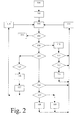
- Figure 2 illustrates a flow chart of the operation of an integrated modem circuit according to the invention.
- the integrated modem circuit according to the invention shown in Figure 1 like for example an Asymmetric Digital Subscriber Line modem or ADSL modem or with a Very high speed Digital Subscriber Line modem or VDSL modem etc. comprises a processor-system 1 with filter software 11 for embodying a digital phase locked loop and with control software 12,13 and sample software 14,15 and comprises hardware 2,3 with a transmission path 2 comprising from input to output a mapper 21, a rotor 22 and an inverse Fourier transformator 23 and a receiving path 3 comprising from input to output a Fourier transformator 33, a rotor 32 and a demapper 31.
- Control software 12,13 receives results from filter software 11, and sample software 14,15 receives results from filter software 11 (or alternatively from control software 12,13).
- Filter software 11 receives an input signal from demapper 31, and control software 12,13 controls rotors 22,32 and sample software 14,15 controls transformators 23,33.
- control software 12,13 controls rotors 22,32 and sample software 14,15 controls transformators 23,33.
- filter software 16 may not shown, with filter software 11,16 receiving their same input signal from demapper 31, but with filter software 11 for example synchronizing one of the paths 2,3 and with filter software 16 synchronizing the other path 3,2.
- Filter software 11 embodies a digital phase locked loop filter for synchronizing a modem signal (a signal received from said other modem circuit and flowing through receiving path 3 or a signal to be transmitted to said other modem circuit and flowing through transmitting path 2) with an oscillation signal by comparing both signals with each other and generating an error signal.
- filter software 11 receives an input signal from demapper 31 and for example filters (calculates) a difference signal between this input signal and an oscillation signal and integrates and/or further filters said difference signal.
- Said oscillation signal may be a real oscillation signal or a calculated oscillation signal or for example a signal flowing through one of the paths etc.
- Sample software 14,15 processes samples of packet signals present in transformators 23,33 in dependence of results originating from said phase locked loop filter by for example shifting samples and/or adding (at one side) and deleting (at the other side) samples of these packet signals for making signal adaptations (for example phase corrections).
- Said rotor(s) 22,32 compensate for said shifting/adding/deleting of samples by rotating the signal correspondingly: shifting samples and/or adding samples at one side and deleting samples at the other side in a window larger than said packet signal (and therefore comprising more samples than said packet signal to allow said shifting and/or adding and deleting) will result in a rotation of the (complex) signal (in the frequency domain), which rotation is compensated by said rotors 22,32.
- Control software 12,13 controls said rotors 22,32 in dependence of results originating from said filter software 11, and said transformators 23,33 are controlled by results originating from said sample software 14,15. Small errors may be corrected by just using said rotors 22,32, larger errors will need sample corrections (shifts and/or additions and deletions) and corresponding rotations.
- Control software 12 for example comprises a rotor filter, and control software 13 for example comprises an integrator.
- the correction in the time domain by transformators 23 and 33 is compensated by a rotation in rotors 22 and 32.
- This rotation is applied on (preferably all) frequency carriers interchanged between rotor 22 and transformator 23 or transformator 33 and rotor 32.
- This rotation means that (preferably all) carrier's amplitudes are not changed (substantially), but their phases are changed with respect to the shift in time that has been applied by said transformators 23 and 33.
- Processor-system 1 further comprises one or more processors and one or more memories not shown.
- Transmission path 2 may further comprise a module for tuning a gain and situated between mapper 21 and rotor 22 or between rotor 22 and transformator 23, and may further comprise a windowing module coupled to an output of transformator 23 and/or a front-end module coupled to an output of said windowing module etc.
- Transmission path 2 operates left of transformator 23 (mapper 21 and rotor 22) in the frequency domain and right of transformator 23 in the time domain.
- Receiving path 3 may further comprise a windowing module coupled to an input of transformator 33 and/or a front-end module coupled to an input of said windowing module, and may further comprise a module for equalizing predefined signals and/or a module for canceling predefined signals and situated between demapper 31 and rotor 32 or between rotor 32 and transformator 33 etc.
- Receiving path 3 operates left of transformator 33 (demapper 31 and rotor 32) in the frequency domain and right of transformator 33 in the time domain.
- the operation of the integrated modem circuit according to the invention as illustrated by the flow chart shown in Figure 2 is as follows.
- Block 102 Reading step, goto 103.
- the structure software detects whether a STOP instruction is present (Block 103: Detection step for finishing in response to a detection of STOP, if positive detection goto 119, if not goto 104). If no STOP instruction is detected in said software part, the structure software detects whether an IF instruction is present (Block 104: Detection step for detecting IF_XX, if positive detection goto 110, if not goto 105).
- Block 107 Detection step of execution type, if first type goto 108, if second type goto 109) and performs this execution or these executions
- Block 108 Execution step for performing an execution of a first type, goto 114
- Block 109 Execution step for performing an execution of a second type, goto 114).
- Block 110 Adaptation step for making adaptations
- the logical comparison operation is performed in block 111) (goto 111).
- the invention is based upon an insight, inter alia, that, at high speeds, hardware phase locked loops are expensive and not accurate sufficiently and offer no flexibility and that, at high speeds, software phase locked loops are not fast enough to make the signal adaptations, and is based upon a basic idea, inter alia, that, at high speeds, the phase locked loop calculations (filtering) should be done in software and that, at high speeds, the compensations (signal adaptations) should be done in hardware.
- the invention solves the problem, inter alia, of providing an integrated modem circuit as defined in the preamble, which can operate at a much higher speed, and is advantageous, inter alia, in that it is low cost, accurate, flexible, and in that it offers the simultaneous design of hardware parts and of software parts.
Priority Applications (2)
| Application Number | Priority Date | Filing Date | Title |
|---|---|---|---|
| EP02293129A EP1432193A1 (de) | 2002-12-18 | 2002-12-18 | Integrierte Modem Schaltung mit softwareimplementation eines PLL Filter |
| US10/736,755 US20040125872A1 (en) | 2002-12-18 | 2003-12-17 | Integrated modem circuit operating at 1 Mbit/s or more |
Applications Claiming Priority (1)
| Application Number | Priority Date | Filing Date | Title |
|---|---|---|---|
| EP02293129A EP1432193A1 (de) | 2002-12-18 | 2002-12-18 | Integrierte Modem Schaltung mit softwareimplementation eines PLL Filter |
Publications (1)
| Publication Number | Publication Date |
|---|---|
| EP1432193A1 true EP1432193A1 (de) | 2004-06-23 |
Family
ID=32338195
Family Applications (1)
| Application Number | Title | Priority Date | Filing Date |
|---|---|---|---|
| EP02293129A Withdrawn EP1432193A1 (de) | 2002-12-18 | 2002-12-18 | Integrierte Modem Schaltung mit softwareimplementation eines PLL Filter |
Country Status (2)
| Country | Link |
|---|---|
| US (1) | US20040125872A1 (de) |
| EP (1) | EP1432193A1 (de) |
Families Citing this family (1)
| Publication number | Priority date | Publication date | Assignee | Title |
|---|---|---|---|---|
| KR100592902B1 (ko) * | 2003-12-27 | 2006-06-23 | 한국전자통신연구원 | 적응형 주파수 제어 장치 및 그 방법 |
Citations (3)
| Publication number | Priority date | Publication date | Assignee | Title |
|---|---|---|---|---|
| US5727038A (en) * | 1996-09-06 | 1998-03-10 | Motorola, Inc. | Phase locked loop using digital loop filter and digitally controlled oscillator |
| US5790594A (en) * | 1995-07-28 | 1998-08-04 | Motorola, Inc. | High speed modem and method for expedited timing recovery |
| US6215363B1 (en) * | 1999-09-27 | 2001-04-10 | Conexant Systems, Inc. | Low noise low power charge pump system for phase lock loop |
Family Cites Families (8)
| Publication number | Priority date | Publication date | Assignee | Title |
|---|---|---|---|---|
| US5355365A (en) * | 1993-03-31 | 1994-10-11 | Multi-Tech Systems, Inc. | Intelligent local area network modem node |
| US6088386A (en) * | 1996-07-15 | 2000-07-11 | Alcatel | Transmitter with phase rotor, modulator/demodulator, communication system and method performed thereby |
| US6603808B1 (en) * | 1999-07-22 | 2003-08-05 | Compaq Information Technologies Group, L.P. | Dual mode phone line networking modem utilizing conventional telephone wiring |
| EP1128623A1 (de) * | 2000-02-24 | 2001-08-29 | Alcatel | Verfahren zur Minimizierung der Sendeleistung von nicht-aktiven ATM Zellen in einem XDSL System mit trelliskodierter Modulation |
| US6877043B2 (en) * | 2000-04-07 | 2005-04-05 | Broadcom Corporation | Method for distributing sets of collision resolution parameters in a frame-based communications network |
| EP1162777A1 (de) * | 2000-06-07 | 2001-12-12 | Alcatel | Mehrträger-Kommunikationsystem mit Abtastratenpilotkanal und Zeitduplexrasterfrequenz-pilotkanal |
| US6539081B2 (en) * | 2001-07-20 | 2003-03-25 | Adtran Inc. | Method of establishing signaling rate for single-line digital subscriber link providing extended range ADSL service with auxiliary pots channel |
| US20030112966A1 (en) * | 2001-12-18 | 2003-06-19 | Bijit Halder | Method and system for implementing a reduced complexity dual rate echo canceller |
-
2002
- 2002-12-18 EP EP02293129A patent/EP1432193A1/de not_active Withdrawn
-
2003
- 2003-12-17 US US10/736,755 patent/US20040125872A1/en active Pending
Patent Citations (3)
| Publication number | Priority date | Publication date | Assignee | Title |
|---|---|---|---|---|
| US5790594A (en) * | 1995-07-28 | 1998-08-04 | Motorola, Inc. | High speed modem and method for expedited timing recovery |
| US5727038A (en) * | 1996-09-06 | 1998-03-10 | Motorola, Inc. | Phase locked loop using digital loop filter and digitally controlled oscillator |
| US6215363B1 (en) * | 1999-09-27 | 2001-04-10 | Conexant Systems, Inc. | Low noise low power charge pump system for phase lock loop |
Non-Patent Citations (1)
| Title |
|---|
| SOLLENBERGER N R ET AL: "Architecture and implementation of an efficient and robust TDMA frame structure for digital portable communications", IEEE, 1989, pages 169 - 173, XP010086250 * |
Also Published As
| Publication number | Publication date |
|---|---|
| US20040125872A1 (en) | 2004-07-01 |
Similar Documents
| Publication | Publication Date | Title |
|---|---|---|
| KR100945688B1 (ko) | 수신기에서 신호 불균형에 대한 보상을 위한 장치 및 방법 | |
| JP2712706B2 (ja) | 適応位相検出同期方法 | |
| JP2765600B2 (ja) | 復調回路 | |
| US6965617B2 (en) | Resynchronous control apparatus of subscriber communication machine, and resynchronizing method | |
| US7916822B2 (en) | Method and apparatus for reducing latency in a clock and data recovery (CDR) circuit | |
| WO2000014650A1 (en) | A method of frequency domain filtering employing a real to analytic transform | |
| CN101789773A (zh) | 占空比偏移检测和补偿电路 | |
| EP1432193A1 (de) | Integrierte Modem Schaltung mit softwareimplementation eines PLL Filter | |
| CA1191206A (en) | Full duplex modems and synchronizing methods and apparatus therefor | |
| JPS5938780B2 (ja) | デジタル・モデムを同期する方式 | |
| CN110247751A (zh) | 正交幅度调制qam信号位同步的方法、装置及存储介质 | |
| JP3789275B2 (ja) | 副搬送波周波数信号復調装置 | |
| EP0987864A1 (de) | Zeitfehlerkompensationsanordnung und diese umfassendes Mehrträgermodem | |
| US5648994A (en) | Digital phase-locked loop | |
| CN1299461C (zh) | 用于均衡器更新和采样速率控制的方法和设备 | |
| EP0316842B1 (de) | Vorrichtung zur Phasensteuerung | |
| EP1071269A1 (de) | Übertragungsverfahren für teilnehmerleitung | |
| US20040047410A1 (en) | Method and apparatus for compensating for phase error of digital signal | |
| KR100575565B1 (ko) | Dsl 모뎀 장치 및 dsl 통신을 위한 통신 제어 방법 | |
| JPS6117384B2 (de) | ||
| KR100333706B1 (ko) | 고속 및 저잡음을 위한 심볼 타이밍 에러의 판별 및 복원 장치 | |
| KR0155935B1 (ko) | 위상 지터 트래커를 갖는 캐리어 복구 방법 및 장치 | |
| JP3278907B2 (ja) | 搬送波補正装置 | |
| CN114785475A (zh) | 一种Gardner定时误差检测的增强方法 | |
| JPS6272250A (ja) | ル−プネツトワ−ク装置 |
Legal Events
| Date | Code | Title | Description |
|---|---|---|---|
| PUAI | Public reference made under article 153(3) epc to a published international application that has entered the european phase |
Free format text: ORIGINAL CODE: 0009012 |
|
| AK | Designated contracting states |
Kind code of ref document: A1 Designated state(s): AT BE BG CH CY CZ DE DK EE ES FI FR GB GR IE IT LI LU MC NL PT SE SI SK TR |
|
| AX | Request for extension of the european patent |
Extension state: AL LT LV MK RO |
|
| 17P | Request for examination filed |
Effective date: 20041223 |
|
| AKX | Designation fees paid |
Designated state(s): AT BE BG CH CY CZ DE DK EE ES FI FR GB GR IE IT LI LU MC NL PT SE SI SK TR |
|
| RAP1 | Party data changed (applicant data changed or rights of an application transferred) |
Owner name: ALCATEL LUCENT |
|
| 17Q | First examination report despatched |
Effective date: 20070531 |
|
| STAA | Information on the status of an ep patent application or granted ep patent |
Free format text: STATUS: THE APPLICATION IS DEEMED TO BE WITHDRAWN |
|
| 18D | Application deemed to be withdrawn |
Effective date: 20090227 |