EP1429325A1 - Optical recording medium manufacturing method - Google Patents
Optical recording medium manufacturing method Download PDFInfo
- Publication number
- EP1429325A1 EP1429325A1 EP02763015A EP02763015A EP1429325A1 EP 1429325 A1 EP1429325 A1 EP 1429325A1 EP 02763015 A EP02763015 A EP 02763015A EP 02763015 A EP02763015 A EP 02763015A EP 1429325 A1 EP1429325 A1 EP 1429325A1
- Authority
- EP
- European Patent Office
- Prior art keywords
- layer
- energy ray
- disk
- light
- recording medium
- Prior art date
- Legal status (The legal status is an assumption and is not a legal conclusion. Google has not performed a legal analysis and makes no representation as to the accuracy of the status listed.)
- Withdrawn
Links
Images

Classifications
-
- B—PERFORMING OPERATIONS; TRANSPORTING
- B29—WORKING OF PLASTICS; WORKING OF SUBSTANCES IN A PLASTIC STATE IN GENERAL
- B29C—SHAPING OR JOINING OF PLASTICS; SHAPING OF MATERIAL IN A PLASTIC STATE, NOT OTHERWISE PROVIDED FOR; AFTER-TREATMENT OF THE SHAPED PRODUCTS, e.g. REPAIRING
- B29C71/00—After-treatment of articles without altering their shape; Apparatus therefor
- B29C71/02—Thermal after-treatment
-
- B—PERFORMING OPERATIONS; TRANSPORTING
- B29—WORKING OF PLASTICS; WORKING OF SUBSTANCES IN A PLASTIC STATE IN GENERAL
- B29C—SHAPING OR JOINING OF PLASTICS; SHAPING OF MATERIAL IN A PLASTIC STATE, NOT OTHERWISE PROVIDED FOR; AFTER-TREATMENT OF THE SHAPED PRODUCTS, e.g. REPAIRING
- B29C71/00—After-treatment of articles without altering their shape; Apparatus therefor
- B29C71/04—After-treatment of articles without altering their shape; Apparatus therefor by wave energy or particle radiation, e.g. for curing or vulcanising preformed articles
-
- G—PHYSICS
- G11—INFORMATION STORAGE
- G11B—INFORMATION STORAGE BASED ON RELATIVE MOVEMENT BETWEEN RECORD CARRIER AND TRANSDUCER
- G11B7/00—Recording or reproducing by optical means, e.g. recording using a thermal beam of optical radiation by modifying optical properties or the physical structure, reproducing using an optical beam at lower power by sensing optical properties; Record carriers therefor
- G11B7/24—Record carriers characterised by shape, structure or physical properties, or by the selection of the material
- G11B7/26—Apparatus or processes specially adapted for the manufacture of record carriers
-
- B—PERFORMING OPERATIONS; TRANSPORTING
- B29—WORKING OF PLASTICS; WORKING OF SUBSTANCES IN A PLASTIC STATE IN GENERAL
- B29C—SHAPING OR JOINING OF PLASTICS; SHAPING OF MATERIAL IN A PLASTIC STATE, NOT OTHERWISE PROVIDED FOR; AFTER-TREATMENT OF THE SHAPED PRODUCTS, e.g. REPAIRING
- B29C35/00—Heating, cooling or curing, e.g. crosslinking or vulcanising; Apparatus therefor
- B29C35/02—Heating or curing, e.g. crosslinking or vulcanizing during moulding, e.g. in a mould
- B29C35/08—Heating or curing, e.g. crosslinking or vulcanizing during moulding, e.g. in a mould by wave energy or particle radiation
- B29C35/0805—Heating or curing, e.g. crosslinking or vulcanizing during moulding, e.g. in a mould by wave energy or particle radiation using electromagnetic radiation
- B29C2035/0827—Heating or curing, e.g. crosslinking or vulcanizing during moulding, e.g. in a mould by wave energy or particle radiation using electromagnetic radiation using UV radiation
-
- B—PERFORMING OPERATIONS; TRANSPORTING
- B29—WORKING OF PLASTICS; WORKING OF SUBSTANCES IN A PLASTIC STATE IN GENERAL
- B29C—SHAPING OR JOINING OF PLASTICS; SHAPING OF MATERIAL IN A PLASTIC STATE, NOT OTHERWISE PROVIDED FOR; AFTER-TREATMENT OF THE SHAPED PRODUCTS, e.g. REPAIRING
- B29C35/00—Heating, cooling or curing, e.g. crosslinking or vulcanising; Apparatus therefor
- B29C35/02—Heating or curing, e.g. crosslinking or vulcanizing during moulding, e.g. in a mould
-
- G—PHYSICS
- G11—INFORMATION STORAGE
- G11B—INFORMATION STORAGE BASED ON RELATIVE MOVEMENT BETWEEN RECORD CARRIER AND TRANSDUCER
- G11B7/00—Recording or reproducing by optical means, e.g. recording using a thermal beam of optical radiation by modifying optical properties or the physical structure, reproducing using an optical beam at lower power by sensing optical properties; Record carriers therefor
- G11B7/24—Record carriers characterised by shape, structure or physical properties, or by the selection of the material
- G11B7/26—Apparatus or processes specially adapted for the manufacture of record carriers
- G11B7/265—Apparatus for the mass production of optical record carriers, e.g. complete production stations, transport systems
Definitions
- the present invention relates to a method for manufacturing an optical recording medium and, more particularly, to a method for manufacturing an optical recording medium having on a recording layer a light-transmitting layer formed of an energy ray-curable resin.
- DVDs In which the wavelength of a recoding and reproducing laser beam is made shorter and the numerical aperture (NA) of an objective lens is made larger so that the diameter of a focal spot produced during recording or reproducing is reduced.
- the recording and reproducing wavelength ⁇ of 780 nm used in CDs is changed to 650 nm in DVDs, and the numerical aperture (NA) of 0.45 used in CDs to 0.6 in DVDs, whereby a recording capacity increased to 6- to 8-fold that of CDs (4.7GB per side) has been achieved.
- the increased numerical aperture will raise various problems.
- the increased numerical aperture decreases the allowance for aberration produced due to an angle by which a disk surface is deviated from the perpendicular to the optical axis of an optical pickup, which is known as a tilt angle.
- an allowance for tilt of an optical recording medium with respect to an optical system which is known as a tilt margin M
- NA an allowance for tilt of an optical recording medium with respect to an optical system
- NA a numerical aperture
- the tilt margin M is proportional to ⁇ / ⁇ t ⁇ (NA) 3 ⁇ when ⁇ denotes a wavelength of a recording and reproducing laser beam, and t denotes a thickness of a substrate. Therefore, in order to ensure a sufficient tilt margin M, it is required to reduce the thickness t of a substrate.
- a sufficient tilt margin is ensured by reducing the substrate thickness to about one half (about 0.6mm) of a typical thickness of conventional CD substrates (about 1.2mm).
- the recording and reproducing laser beam is irradiated not to the substrate side but through a light-transmitting layer formed with a thickness of about 0.1mm.
- An optical recording medium having such a light-transmitting layer is disclosed, for example, in Japanese Patent Laid-Open Publication No. Hei 10-289489, and the medium disclosed in this patent publication has a light-transmitting layer comprising a photo-curable resin.
- an energy ray-curable resin is used for a protective layer, which poses a problem of increased warping of the media due to shrinkage on curing of the resin. Therefore, various studies and attempts have been made to decrease such shrinkage on curing in view of materials.
- the thickness of the coated film of the energy ray-curable resin for the protective layer is only about 2 ⁇ m to 20 ⁇ m, sufficient studies have not been focused on those having a larger thickness.
- a further object of the present invention is to provide an apparatus for manufacturing an optical recording medium suitable for use in the above-mentioned method.
- the present inventors After earnest researches, the present inventors have found that, by employing an energy ray-curable resin having a relatively low degree of shrinkage on curing and allowing the resin to cure stepwise, it is possible to disperse the stress generated by the shrinkage on curing of the resin to minimize the stress accumulated in a disk, and thus to obtain an optical recording medium with minimal deformation in the disk and with superior mechanical properties.
- the present invention thus has been achieved.
- the present inventors have further found that, by releasing the stress accumulated in the disk by annealing, and then allowing the resin to cure again, the optical information medium can be obtained with further improved mechanical properties.
- the present invention is a method for manufacturing an optical recording medium having, on a supporting substrate, at least one recording layer and a light-transmitting layer on the recording layer, comprising the steps of providing an energy ray-curable resin layer on the recording layer, and irradiating the resin layer with an energy ray at least twice to form a light-transmitting layer.
- the present invention is the above-described method for manufacturing an optical recording medium wherein an integrated quantity of light of each energy ray irradiation is increased stepwise between respective two consecutive irradiations.
- the present invention is the above-described method for manufacturing an optical recording medium wherein an annealing step (thermal relaxation step) is conducted between any one energy ray irradiation and a successive energy ray irradiation.
- an annealing step thermal relaxation step
- the present invention is the above-described method for manufacturing an optical recording medium wherein the annealing step is conducted at a temperature of 60°C or higher.
- the present invention is the above-described method for manufacturing an optical recording medium wherein the thickness of the light-transmitting layer is in a range of 20 to 200 ⁇ m.
- the present invention relates to an apparatus for manufacturing an optical recording medium suitable for use in the above-mentioned method.
- the apparatus for manufacturing an optical recording medium of the present invention comprises:
- optical disk A method for manufacturing an optical recording medium (for brevity to be referred to hereinafter as "optical disk") will be described with reference to the drawings.
- optical disk phase change type optical disk
- the present invention is not limited to this, but is widely applicable to various optical disks with any type of recording layers, including read-only optical disks, and single-recordable optical disks and the like.
- Fig. 1 schematically shows a cross section of an example of an optical disk manufactured by a method of the present invention.
- an optical disk (1) has a supporting substrate (2) having information pits, pregrooves, and other fine scale convex-concave formed on one surface thereof.
- the optical disk (1) has a reflective layer (3), a dielectric layer (4), a recording layer (5), and a dielectric layer (6) formed in this order, and further has a light-transmitting layer (7) on the dielectric layer (6).
- the disk (1) also has a central hole (8).
- a laser beam for recording or reproduction is introduced through the light-transmitting layer (7).
- the supporting substrate (2) has a thickness of 0.3 to 1.6mm, preferably of 0.5 to 1.3mm, and includes information pits, pregrooves, and other fine scale convex-concave formed on the surface on which the recording layer (5) is formed.
- the supporting substrate (2) is not required to be optically transparent and may be used various plastic materials including polycarbonate resins, acrylic resins such as polymethyl methacrylate (PMMA), and polyolefine resins and the like. Such flexible materials are particularly useful in the present invention since they can control the warping. It should be noted, however, that glass, ceramics or metals and the like may be also used for the supporting substrate. If a plastic material is employed, the pattern of the convex-concave in the surface will be often produced by injection molding, whereas the pattern will be formed by a photopolymer process (2P process) in the case of any material other than plastics.
- 2P process photopolymer process
- the reflective layer (3) is usually formed by a sputtering process on the supporting substrate (2).
- a material for the reflective layer a metallic element, semi-metallic element, semiconductor element or a compound thereof may be used singly or compositely. More specifically, the material may be selected from known materials for the reflective layers such as Au, Ag, Cu, Al, and Pd.
- the reflective layer is preferably formed as a thin film with a thickness of 20 to 200nm.
- the dielectric layer (4), the recording layer (5), and the dielectric layer (6) are formed in this order by sputtering process on the reflective layer (3), or on the supporting substrate (2) in the case that no reflective layer is provided.
- the recording layer (5) is formed of a material changing reversibly by irradiation of laser beam between the crystalline state and the amorphous state, and exhibiting different optical properties between these states.
- examples of such material include Ge-Sb-Te, In-Sb-Te, Sn-Se-Te, Ge-Te-Sn, In-Se-Tl, and In-Sb-Te.
- a trace of at least one metal selected from Co, Pt, Pd, Au, Ag, Ir, Nb, Ta, V, W, Ti, Cr, Zr, Bi, In and the like may be added.
- a trace of reductive gas such as nitrogen also may be added.
- the thickness of the recording layer (5) which is for example in a range of about 3 to 50nm.
- the dielectric layers (4) and (6) is preferably formed of an oxide, a nitride, a sulfide, or a fluoride or a composite thereof, containing at least one metal selected from Si, Zn, Al, Ta, Ti, Co, Zr, Pb, Ag, Zn, Sn, Ca, Ce, V, Cu, Fe, and Mg. Further, the dielectric layers (4) and (6) preferably have an extinction coefficient k of 0.1 or less.
- the thickness of the dielectric layer (4) which is preferably for example in a range of about 20 to 150nm.
- the thickness of the dielectric layer (6) either, which is preferably for example in a range of about 20 to 200nm. Setting the thicknesses of the dielectric layers (4) and (6) in these ranges makes it possible to adjust reflection.
- the light-transmitting layer (7) is formed on the dielectric layer (6) by using energy ray-curable resin.
- the energy ray-curable resin should be optically transparent, exhibit low optical absorption or reflection in the laser wavelength range to be used, and have low birefringence, and is selected from ultraviolet ray-curable resins, electron ray-curable resins and the like on these conditions.
- the energy ray-curable resin is constituted preferably of the ultraviolet- (electro-) curable compound or its composition for polymerization.
- examples include monomers, oligomers, polymers and the like in which groups to be crosslinked or polymerized by irradiation with UV rays, such as acrylic type double bonds such as in ester compounds of acrylate and methacrylate, epoxy acrylates and urethane acrylates, allyl type double bonds such as in diallyl phthalate, and unsaturated double bonds such as in maleic acid derivatives and the like have been contained or introduced into a molecule.
- groups to be crosslinked or polymerized by irradiation with UV rays such as acrylic type double bonds such as in ester compounds of acrylate and methacrylate, epoxy acrylates and urethane acrylates, allyl type double bonds such as in diallyl phthalate, and unsaturated double bonds such as in maleic acid derivatives and the like have been contained or introduced into a molecule
- the ultraviolet-curable monomer is preferably a compound with a molecular weight of less than 2000
- the oligomer is preferably a compound with a molecular weight of 2000 to 10000.
- These include styrene, ethyl acrylate, ethylene glycol diacrylate, ethylene glycol dimethacrylate, diethylene glycol diacrylate, diethylene glycol methacrylate, 1,6-hexane glycol diacrylate, 1,6-hexane glycol dimethacrylate etc.
- particularly preferable examples include pentaerythritol tetra(meth)acrylate, pentaerythritol (meth)acrylate, trimethylolpropane tri(meth)acrylate, trimethylolpropane di(meth)acrylate, (meth)acrylate of phenol ethylene oxide adduct, etc.
- the ultraviolet-curable oligomer includes oligoester acrylate, acrylic modified urethane
- the ultraviolet-curable material a composition containing epoxy resin and a photo-cation polymerization catalyst is also preferably used.
- the epoxy resin is preferably alicyclic epoxy resin, particularly the resin having 2 or more epoxy groups in the molecule.
- the alicyclic epoxy resin is preferably one or more of the following resins: 3,4-epoxycyclohexyl methyl-3,4-epoxycyclohexane carboxylate, bis-(3,4-epoxycyclohexylmethyl) adipate, bis-(3,4-epoxycyclohexyl) adipate, 2-(3,4-epoxycyclohexyl-5,5-spiro-3,4-epoxy) cyclohexane-metha-dioxane, bis(2,3-epoxycyclopentyl) ether and vinyl cyclohexene dioxide etc.
- the epoxy equivalent of alicyclic epoxy resin is not particularly limited, it is preferably 60 to 300,
- the photo-cation polymerization catalyst used may be any of known ones and is not particularly limited.
- metal fluoroborates and boron trifluoride complexes bis(perfluoroalkyl sulfonyl) methane metal salts, aryl diazonium compounds, aromatic onium salts of the group 6A elements, aromatic onium salts of the group 5A elements, dicarbonyl chelate of the groups 3A to 5A elements, thiopyrylium salts, the group 6A elements having MF6 anions (M is P, As or Sb), triaryl sulfonium complex salts, aromatic iodonium complex salts, aromatic sulfonium complex salts etc., and it is particularly preferable to use one or more of the followings: polyaryl sulfonium complex salts, aromatic sulfonium salts or iodonium salts of halogen-containing complex ions, and aromatic
- the radiation curable resin used for the light-transmitting layer preferably has a viscosity of 1,000 to 10,000cp (at 25°C).
- an energy ray-curable resin is applied on the dielectric layer (6) to provide an uncured energy ray-curable resin layer thereon.
- the application may be performed by spin coating process.
- the uncured energy ray-curable layer is irradiated with an energy ray for a plurality of times so as to cure the resin stepwise. Specifically, the irradiation is performed at least twice, an irradiation for curing the resin to the half-cured state but not to the completely cured state and another irradiation for curing the resin from the half-cured state to the completely cured state. Either ultraviolet ray or electron ray may be used as the energy ray depending on the used resin.
- the first energy ray irradiation is performed in such an integrated quantity of light as to leave tackiness on the surface of the resin layer, and to cure the resin up to the half-cured state. Curing the resin to the half-cured state is enabled by shortening the irradiation time or reducing the irradiation intensity, depending on the resin material, in comparison with the case where the resin is cured completely by one irradiation. Such energy ray irradiation is conducted once, or twice or more before the resin is completely cured. If two or more irradiations before complete curing of the resin are performed, the integrated quantity of light is increased stepwise between respective consecutive two energy beam irradiations.
- the final energy beam irradiation is conducted for curing the resin completely, with an integrated quantity of light increased in comparison with any of the integrated quantities of light used in the previous energy ray irradiations, so that the resin is cured to the completely cured state.
- This complete curing is enabled by lengthening the irradiation time or increasing the irradiation intensity in comparison with any of the irradiations before complete curing of the resin.
- the integrated quantity of light used in the respective energy ray irradiations depends on the resin material or the thickness of the resin layer and the like, and is adjusted to be about 5 to 300mJ/cm 2 for the first energy ray irradiation, and about 500 to 5000mJ/cm 2 for the second energy ray irradiation.
- Curing the resin stepwise in this manner makes it possible to decrease the stress accumulated at a time in the disk due to the shrinkage on curing, and hence the stress ultimately accumulated in the disk is decreased.
- the light-transmitting layer (7) has a large thickness of no less than 20 ⁇ m but no more than 200 ⁇ m, particularly no less than 70 ⁇ m but no more than 150 ⁇ m, more particularly no less than 75 ⁇ m but no more than 150 ⁇ m, it is possible to produce a disk with superior mechanical properties.
- the stress due to shrinkage on curing becomes maximum at the moment of the curing of the resin and then is relaxed gradually as the passage of time. Therefore, the stress accumulated in the disk due to the shrinkage on curing can be decreased further, by releasing once the stress accumulated in the disk followed by conducing the next curing. Since it will not be productive if the resin is left in the half-cured state for a long period of time before the stress is released, it is also possible to release the stress in a short period of time by conducting an annealing treatment before curing the resin by irradiating the resin again with an energy ray.
- a more preferable result can be obtained by conducting an annealing treatment after one energy ray irradiation and before the following energy ray irradiation. If three or more energy ray irradiations are to be performed, it is preferable, in view of the release of stress due to shrinkage on curing, to conduct an annealing treatment every time one irradiation is completed, namely between the first and second irradiations, between the second and third irradiations and onwards.
- the annealing temperature is preferably 60°C or higher, and more preferably 80°C or higher.
- the annealing temperature of 80°C or higher enables the complete release of stress to be done more quickly.
- the upper limit of annealing temperature depends on a material used for the supporting substrate, but generally and preferably is a temperature at least 10°C lower than the glass transition temperature Tg of the material used.
- the annealing time, depending on the annealing temperature, is preferably one to five minutes in terms of production efficiency.
- an uncured energy ray-curable resin layer is formed to a thickness corresponding to a part of a target thickness of the light-transmitting layer (7), this resin is irradiated with an energy ray to be half-cured, the same resin is again applied on the half-cured resin layer to a thickness corresponding to the remainder of the target thickness, and then an energy beam is irradiated to completely cure the half-cured resin layer and simultaneously to cure the uncured resin layer.
- mixing occurs in the interface between the two resin layers, and thereby the adhesion between the resin layers can be enhanced.
- an optical disk (11) has a supporting substrate (12) having information pits, pregrooves, and other fine scale convex-concave formed on one surface thereof.
- the optical disk (11) has a dielectric layer (14) for second recording layer, a second recording layer (layer 1) (15), a dielectric layer (16) for second recording layer, a space layer (21), a dielectric layer (18) for first recording layer, a first recording layer (layer 0) (19), and a dielectric layer (20) for first recording layer provided in this order, and further has a light-transmitting layer (17) on the dielectric layer (20).
- the disk (11) also has a central hole (22).
- reflective layers may be provided between the supporting substrate (12) and the dielectric layer (14), and between the space layer (21) and the dielectric layer (18), respectively.
- a laser beam for recording or reproduction is introduced through the light-transmitting layer (17).
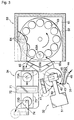
- Fig. 3 is a partially cutaway plan view schematically showing a preferred manufacturing apparatus suitable for use in the manufacturing method of the present invention.
- a manufacturing apparatus for an optical recording medium includes a spin coating unit (31) for coating a supporting substrate with an energy ray-curable resin to provide an energy ray-curable resin layer, a first ultraviolet ray irradiation unit (32) for irradiating the energy ray-curable resin layer with an energy ray to cure the same into a half-cured resin layer, an annealing unit (33) for heating the half-cured resin layer, and a second ultraviolet ray irradiation unit (34) for irradiating the half-cured resin layer with an energy ray to cure the same into a completely cured resin layer.
- a spin coating unit (31) for coating a supporting substrate with an energy ray-curable resin to provide an energy ray-curable resin layer
- a first ultraviolet ray irradiation unit (32) for irradiating the energy ray-curable resin layer with an energy ray to cure the same into a half-cured resin layer
- an annealing unit (33) for heating the half-cured resin layer
- the spin coating unit (31) includes a disk feeder (41) for feeding a disk to be formed with a light-transmitting layer, a horizontal rotary table (42) for carrying and rotating a disk, and a discharge nozzle (43) for dropping an energy ray-curable resin liquid onto the disk surface.
- the disk feeder (41) is provided at the tip end thereof with a vacuum pad for suction holding a disk, and is capable of transporting and feeding a disk by vertical movement and horizontal turning movement of 90 degrees.
- the discharge nozzle (43) is attached to a horizontal arm (45) fixed to a reversibly rotating vertical rotating shaft (44), so that the discharge nozzle (43) rotates horizontally along with rotation of the vertical rotating shaft (44).
- a liquid to be applied is supplied to the discharge nozzle (43) through a liquid supply tube (46) and is dropped from the tip end of the nozzle.
- the first ultraviolet ray irradiation unit (32) includes a body (51), an irradiation head (52) arranged above a disk mounted on the rotary table (42), and a connecting cylinder (53) that connects the body (51) with the irradiation head (52).
- a super-high pressure mercury lamp is provided as an ultraviolet ray source within the body (51).
- a condensing and emitting optical system is further provided within the body (51) so that an ultraviolet ray from the super-high pressure mercury lamp is condensed and emitted as an ultraviolet beam directed to the connecting cylinder (53).
- the connecting cylinder (53) has a cylindrical shape and an integrator lens is incorporated therein so that the ultraviolet beam passes through the cylinder (53) and enters the irradiation head (52).
- the irradiation head (52) has a reflecting plate incorporated therein so that the ultraviolet beam incident from the cylinder (53) is reflected back at 90 degrees and directed to a disk below.
- the annealing unit (33) includes an annealing chamber (61), and a coating hand (65) for transporting a disk on the rotary table (42) of the spin coating unit (31) to a predetermined position in the annealing chamber (61) and simultaneously transporting an annealed disk to the second ultraviolet ray irradiation unit (34) for the following process.
- the annealing chamber (61) is provided with a rotary table (62), and an appropriate number of infrared-ray flat panel heaters (64) arranged over the rotary table (62).
- the rotary table (62) is provided with twelve disk support portions (63) near the outer periphery thereof for supporting twelve disks at intervals of 30 degrees, and rotates intermittently 30 degrees at a time around the center of the table (62) counterclockwise in the example shown.
- An appropriate device is provided below the rotary table (62) for rotating the same.
- the coating hand (65) is rotatable around its vertical shaft (65c) in a range of 120 degrees.
- the coating hand (65) rotates 60 degrees clockwise from the state as shown in Fig. 3, thereby one arm (65a) of the coating hand (65) is positioned above a disk on the rotary table (42).
- the disk on the rotary table (42) is picked up by a vacuum suction mechanism provided at the tip end of the arm (65a).
- the coating hand (65) then rotates 120 degrees counterclockwise and the arm (65a) is positioned at a predetermined position above the rotary table (62), namely above the disk supporting portion indicated by 63A. In this position, the disk is released from suction and set in one of disk supporting portions (63).
- the other arm (65b) of the coating hand (65) is rotated 60 degrees clockwise from the state as shown in Fig. 3 and positioned above the disk supporting portion indicated by 63A. In this position, an annealed disk on the disk supporting portion indicated by 63A is picked up by a vacuum suction mechanism provided at the tip end of the arm (65b).
- the coating hand (65) then rotates 120 degrees counterclockwise, and the arm (65b) is thereby brought to a position indicated by 73A on a disk moving mechanism (73) of the second ultraviolet ray irradiation unit (34) to be described below. In this position, the disk is released from the suction and set at the position indicated by 73A on the disk moving mechanism (73).
- the second ultraviolet ray irradiation unit (34) includes an ultraviolet lamp (71) supported by an appropriate support member (72), the disk moving mechanism (73) for moving a disk linearly to the left-hand side, and a disk discharger (74) for discharging a disk on which a light-transmitting layer has been formed.
- the disk moving mechanism (73), particulars of which are not shown here, is a well known mechanism that is usually provided in a conveyor-type ultraviolet ray irradiation unit. The disk is moved from the position 73A to the position 73B, and during this movement the disk is irradiated with an ultraviolet ray from the ultraviolet lamp (71).
- the disk discharger (74) has a similar mechanism to that of the disk feeder (41).
- a disk having at least one recording layer on which a light-transmitting layer is to be formed is placed on the rotary table (42) by the disk feeder (41) and held by suction.
- a predetermined amount of an energy ray-curable resin liquid is dropped from the tip end of the discharge nozzle (43) onto the surface of the disk placed on the rotary table (42).
- the disk may be either stationary or rotated.
- the disk is then rotated at a high speed to form a resin layer with a uniform thickness on the surface of the disk.
- the uncured resin layer is irradiated for the first time with an ultraviolet ray from the irradiation head (52) to cure the resin into a desired half-cured state. During this irradiation, the disk continues to rotate.
- the rotation of the disk is stopped and the disk is picked up by the one arm (65a) of the coating hand (65) and is set at a predetermined position on the rotary table (62) of the annealing unit (33), namely at one of the disk support portions (63) indicated by 63A.
- the rotary table' (62) is intermittently rotated counterclockwise in the example shown here by 30 degrees at a time for 360 degrees, while the disk is annealed in the anneal chamber (61) at a predetermined temperature for a predetermined time.
- the temperature and time used herein may be adjusted as required.
- the annealed disk that has returned to the position 63A is picked up by the other arm (65b) of the coating hand (65), and set at the position indicated by 73A of the disk moving mechanism (73) in the second ultraviolet ray irradiation unit (34).
- the disk is moved linearly from the position 73A to the position 73B, while being irradiated with an ultraviolet ray from the ultraviolet lamp (71) to cure the resin into a completely cured state.
- a light-transmitting layer is formed.
- the apparatus described above is capable of performing two ultraviolet ray irradiations and an annealing between these irradiations. However, it is also possible to perform three or more ultraviolet ray irradiations and annealing treatments between two consecutive irradiations by providing the apparatus with more annealing units and ultraviolet ray irradiation units, or using the same apparatus and causing the same to repeat a series of annealing treatments and ultraviolet ray irradiations.
- An optical disk sample was prepared according to the following procedures.
- a 100nm thick reflective layer of an Ag-based alloy was formed by sputtering on the surface of a disk-shaped supporting substrate (made of polycarbonate and having a diameter of 120mm and thickness of 1.1mm) having pre-grooves formed thereon.
- the depth of the pre-grooves was ⁇ /10 in the optical path length at a wavelength ⁇ of 405nm, and the substrate was formed as a land and groove substrate having a recording track pitch of 0.3 ⁇ m.
- a 30nm thick dielectric layer was formed by sputtering on the surface of the reflective layer, using a ZnS (80 mol%)-SiO 2 (20 mol%) target.
- a 12nm thick recording layer was formed by sputtering on the surface of this dielectric layer, using an alloy target consisting of a phase-changing material.
- the composition of the recording layer was based on GeSbTe.
- a 100nm thick dielectric layer was formed by sputtering on the surface of the recording layer, using a ZnS (80 mol%)-SiO 2 (20 mol%) target.
- Mechanical properties of the disk thus obtained (warping angle in the disk's radial direction and warping angle in the disk's circumferential direction) were measured with a machinery accuracy measurement instrument, DC-1010C manufactured by Cores Co., Ltd.
- an ultraviolet ray-curable resin primarily composed of urethane acrylate (with a shrinkage on curing of 5.5% and a viscosity of 5000cP at 25°C) was applied by spin coating on the surface of the top surface of dielectric layer, and was spun at 2000rpm for eight seconds to form a 100 ⁇ m thick uncured resin layer.
- the ultraviolet'ray-curable resin layer thus formed was irradiated with an ultraviolet ray at an integrated quantity of UV light of 140mJ/cm 2 to provide a half-cured resin layer.
- the resin layer was then irradiated with an ultraviolet ray at an integrated quantity of UV light of 3000mJ/cm 2 to cure the resin layer completely, thus forming a light-transmitting layer.
- Mechanical properties of the disk sample thus prepared (warping angle in the disk's radial direction and warping angle in the disk's circumferential direction) were measured with the aforementioned instrument DC-1010C.
- Example 2 The same procedures as in Example 1 were repeated up to the formation of an uncured resin layer.
- the ultraviolet ray-curable resin layer was irradiated with an ultraviolet ray at an integrated quantity of UV light of 140mJ/cm 2 to provide a half-cured resin layer.
- the half-cured resin layer was then annealed at 60°C for three minutes, and thereafter the resin layer was irradiated with an ultraviolet ray at an integrated quantity of UV light of 3000mJ/cm 2 to cure the resin layer completely and thereby form a light-transmitting layer.
- Mechanical properties of the disk sample thus produced were measured with the aforementioned instrument DC-1010C.
- Example 2 The same procedures as in Example 1 were repeated up to the formation of an uncured resin layer.
- the resin layer was irradiated with an ultraviolet ray at an integrated quantity of UV light of 3000mJ/cm 2 without being cured to the half-cured state, so that the resin layer was cured completely to form a light-transmitting layer.
- Mechanical properties of the disk sample thus produced were measured with the aforementioned instrument DC-1010C.
- a disk sample was produced in the same manner as in Example 1 except that a resin having slightly higher shrinkage on curing (shrinkage on curing of 5.9% and viscosity of 5800cP at 25°C) than the resin used in Example 1 was used as the ultraviolet ray-curable resin principally composed of urethane acrylate. Mechanical properties of the disk sample thus produced were measured with the aforementioned instrument DC-1010C.
- Example 3 Using the same resin as used in Example 3 as the ultraviolet ray-curable resin, a disk sample was produced in the same manner as in Example 2 except that annealing was conducted at a temperature of 80°C. Mechanical properties of the disk sample thus produced were measured with the aforementioned instrument DC-1010C.
- a disk sample was produced in the same manner as in Comparative Example 1 except that the same resin as used in Example 3 was used as the ultraviolet ray-curable resin. Mechanical properties of the disk sample thus produced were measured with the aforementioned instrument DC-1010C. before formation of the light-transmitting layer after formation of the light-transmitting layer variation R-Skew deg. T-Skew deg. R-Skew deg. T-Skew deg. ⁇ R-Skew deg. ⁇ T-Skew deg.
- Example 2 -0.249 0.038 0.016 0.055 0.265 0.017
- Comparative Example 1 -0.260 0.043 0.382 0.112 0.642 0.069
- Example 3 -0.259 0.039 0.213 0.060 0.472 0.021
- Example 4 -0.253 0.039 0.144 0.045 0.397 0.006 Comparative Example 2 -0.248 0.045 0.473 0.118 0.721 0.073
- R-Skew denotes a warping angle (degrees) in the radial direction of the disk
- T-Skew denotes a warping angle (degrees) in the circumferential direction of the disk.
- Each warping angle was measured with the light-transmitting layer side of the disk facing the laser head of the measurement instrument. Warping that is concave to the light-transmitting layer side is represented by a positive value, whereas warping that is convex to the light-transmitting layer side is represented by a negative value.
- ⁇ T-Skew (T-Skew after the formation of the light-transmitting layer) - (T-Skew before the formation of the light-transmitting layer).
- Example 4 As seen from Table 1, in all the disk samples of Examples 1 through 4, the shrinkage on curing of the resin due to irradiation of an ultraviolet ray was substantially reduced and the variation between the warping angles before and after the formation of the light-transmitting layer was small, and the disk samples exhibited superior mechanical properties. Particularly, in Example 4, even though the resin having a relatively high shrinkage on curing was used, the disk sample exhibited superior mechanical properties as a merit of the correct annealing treatment applied to the resin.
- an optical recording medium having superior mechanical properties by forming a light-transmitting layer with a thickness of about 0.1mm (100 ⁇ m) using a photo-curable resin. Further, according to the present invention, it is possible to provide an apparatus for manufacturing an optical recording medium suitable for use in such method.
Landscapes
- Engineering & Computer Science (AREA)
- Manufacturing & Machinery (AREA)
- Physics & Mathematics (AREA)
- Thermal Sciences (AREA)
- Manufacturing Optical Record Carriers (AREA)
Abstract
The present invention provides a method for
manufacturing an optical recording medium by forming a
light-transmitting layer employing a photo-curable resin,
yet affording superior mechanical properties. The present
invention also provides an apparatus for manufacturing an
optical recording medium suitable for use in the above-mentioned
method. A method for manufacturing an optical
recording medium (1) having, on a supporting substrate (2),
at least one recording layer (5) and a light-transmitting
layer (7) on the recording layer (5), comprising the steps
of providing an energy ray-curable resin layer on the
recording layer (5), and irradiating the resin layer with
an energy ray at least twice to form the light-transmitting
layer (7).
Description
The present invention relates to a method for
manufacturing an optical recording medium and, more
particularly, to a method for manufacturing an optical
recording medium having on a recording layer a light-transmitting
layer formed of an energy ray-curable resin.
In late years, there has been a need for an optical
recording medium capable of affording still higher recoding
density for processing a huge amount of information such as
dynamic picture image information, and the research and
development have been actively conducted for achieving
increased recording density and capacity in an optical
recording medium.
One example of such achievements is found in DVDs, in
which the wavelength of a recoding and reproducing laser
beam is made shorter and the numerical aperture (NA) of an
objective lens is made larger so that the diameter of a
focal spot produced during recording or reproducing is
reduced. Actually in DVDs, the recording and reproducing
wavelength λ of 780 nm used in CDs is changed to 650 nm in
DVDs, and the numerical aperture (NA) of 0.45 used in CDs
to 0.6 in DVDs, whereby a recording capacity increased to
6- to 8-fold that of CDs (4.7GB per side) has been achieved.
However, the increased numerical aperture will raise
various problems. For example, the increased numerical
aperture decreases the allowance for aberration produced
due to an angle by which a disk surface is deviated from
the perpendicular to the optical axis of an optical pickup,
which is known as a tilt angle. In this relation, an
allowance for tilt of an optical recording medium with
respect to an optical system, which is known as a tilt
margin M, is determined by a numerical aperture NA. In
other words, the tilt margin M is proportional to λ/{t ×
(NA)3} when λ denotes a wavelength of a recording and
reproducing laser beam, and t denotes a thickness of a
substrate. Therefore, in order to ensure a sufficient tilt
margin M, it is required to reduce the thickness t of a
substrate.
Accordingly, in DVDs, a sufficient tilt margin is
ensured by reducing the substrate thickness to about one
half (about 0.6mm) of a typical thickness of conventional
CD substrates (about 1.2mm).
Recently, for the purpose of making it possible to
record a high quality dynamic picture image for long hours,
a system has been developed to achieve a large recording
capacity (larger than 20 GB per side) corresponding to more
than 4-fold that of DVDs by decreasing the wavelength λ of
a recording and reproducing laser beam to about 400nm and
increasing the numerical aperture (NA) to 0.85.
In this system, the recording and reproducing laser
beam is irradiated not to the substrate side but through a
light-transmitting layer formed with a thickness of about
0.1mm. An optical recording medium having such a light-transmitting
layer is disclosed, for example, in Japanese
Patent Laid-Open Publication No. Hei 10-289489, and the
medium disclosed in this patent publication has a light-transmitting
layer comprising a photo-curable resin.
On the other hand, in conventional optical recording
media including CDs and DVDs and the like, an energy ray-curable
resin is used for a protective layer, which poses a
problem of increased warping of the media due to shrinkage
on curing of the resin. Therefore, various studies and
attempts have been made to decrease such shrinkage on
curing in view of materials. However, since the thickness
of the coated film of the energy ray-curable resin for the
protective layer is only about 2µm to 20µm, sufficient
studies have not been focused on those having a larger
thickness.
More specifically, in the case where a light-transmitting
layer having a thickness of about 0.1mm
(100µm) is formed of an energy ray-curable resin, it will
be difficult to solve the problem of shrinkage on curing
only by improvement of the resin material.
In view of the problem as above, an object of the
present invention is to provide a method for manufacturing
an optical recording medium by forming a light-transmitting
layer employing an energy ray-curable resin, yet affording
superior mechanical properties.
A further object of the present invention is to
provide an apparatus for manufacturing an optical recording
medium suitable for use in the above-mentioned method.
After earnest researches, the present inventors have
found that, by employing an energy ray-curable resin having
a relatively low degree of shrinkage on curing and allowing
the resin to cure stepwise, it is possible to disperse the
stress generated by the shrinkage on curing of the resin to
minimize the stress accumulated in a disk, and thus to
obtain an optical recording medium with minimal deformation
in the disk and with superior mechanical properties. The
present invention thus has been achieved.
The present inventors have further found that, by
releasing the stress accumulated in the disk by annealing,
and then allowing the resin to cure again, the optical
information medium can be obtained with further improved
mechanical properties.
The present invention is a method for manufacturing
an optical recording medium having, on a supporting
substrate, at least one recording layer and a light-transmitting
layer on the recording layer, comprising the
steps of providing an energy ray-curable resin layer on the
recording layer, and irradiating the resin layer with an
energy ray at least twice to form a light-transmitting
layer.
The present invention is the above-described method
for manufacturing an optical recording medium wherein an
integrated quantity of light of each energy ray irradiation
is increased stepwise between respective two consecutive
irradiations.
The present invention is the above-described method
for manufacturing an optical recording medium wherein the
energy ray is an ultraviolet ray.
The present invention is the above-described method
for manufacturing an optical recording medium wherein an
annealing step (thermal relaxation step) is conducted
between any one energy ray irradiation and a successive
energy ray irradiation.
The present invention is the above-described method
for manufacturing an optical recording medium wherein the
annealing step is conducted at a temperature of 60°C or
higher.
The present invention is the above-described method
for manufacturing an optical recording medium wherein the
thickness of the light-transmitting layer is in a range of
20 to 200µm.
Further, the present invention relates to an
apparatus for manufacturing an optical recording medium
suitable for use in the above-mentioned method. The
apparatus for manufacturing an optical recording medium of
the present invention comprises:
A method for manufacturing an optical recording
medium (for brevity to be referred to hereinafter as
"optical disk") will be described with reference to the
drawings. Although the description will be given of a
phase change type optical disk as an example, the present
invention is not limited to this, but is widely applicable
to various optical disks with any type of recording layers,
including read-only optical disks, and single-recordable
optical disks and the like.
Fig. 1 schematically shows a cross section of an
example of an optical disk manufactured by a method of the
present invention. In Fig. 1, an optical disk (1) has a
supporting substrate (2) having information pits,
pregrooves, and other fine scale convex-concave formed on
one surface thereof. On this surface, the optical disk (1)
has a reflective layer (3), a dielectric layer (4), a
recording layer (5), and a dielectric layer (6) formed in
this order, and further has a light-transmitting layer (7)
on the dielectric layer (6). The disk (1) also has a
central hole (8). When using the optical disk (1), a laser
beam for recording or reproduction is introduced through
the light-transmitting layer (7).
The supporting substrate (2) has a thickness of 0.3
to 1.6mm, preferably of 0.5 to 1.3mm, and includes
information pits, pregrooves, and other fine scale convex-concave
formed on the surface on which the recording layer
(5) is formed.
The supporting substrate (2) is not required to be
optically transparent and may be used various plastic
materials including polycarbonate resins, acrylic resins
such as polymethyl methacrylate (PMMA), and polyolefine
resins and the like. Such flexible materials are
particularly useful in the present invention since they can
control the warping. It should be noted, however, that
glass, ceramics or metals and the like may be also used for
the supporting substrate. If a plastic material is
employed, the pattern of the convex-concave in the surface
will be often produced by injection molding, whereas the
pattern will be formed by a photopolymer process (2P
process) in the case of any material other than plastics.
The reflective layer (3) is usually formed by a
sputtering process on the supporting substrate (2). As a
material for the reflective layer, a metallic element,
semi-metallic element, semiconductor element or a compound
thereof may be used singly or compositely. More
specifically, the material may be selected from known
materials for the reflective layers such as Au, Ag, Cu, Al,
and Pd. The reflective layer is preferably formed as a
thin film with a thickness of 20 to 200nm.
The dielectric layer (4), the recording layer (5),
and the dielectric layer (6) are formed in this order by
sputtering process on the reflective layer (3), or on the
supporting substrate (2) in the case that no reflective
layer is provided.
The recording layer (5) is formed of a material
changing reversibly by irradiation of laser beam between
the crystalline state and the amorphous state, and
exhibiting different optical properties between these
states. Examples of such material include Ge-Sb-Te, In-Sb-Te,
Sn-Se-Te, Ge-Te-Sn, In-Se-Tl, and In-Sb-Te. Further,
to any such matrial, a trace of at least one metal selected
from Co, Pt, Pd, Au, Ag, Ir, Nb, Ta, V, W, Ti, Cr, Zr, Bi,
In and the like may be added. A trace of reductive gas
such as nitrogen also may be added.
There is no limitation to the thickness of the
recording layer (5), which is for example in a range of
about 3 to 50nm.
The dielectric layers (4) and (6) are formed on the
top and under surfaces of the recording layer (5),
respectively, so as to sandwich the same. The dielectric
layers (4) and (6) have not only a function of protecting
the recording layer (5) mechanically and chemically but
also a function as an interference layer for adjusting the
optical properties. The dielectric layers (4) and (6) may
each consist of either a single layer or a plurality of
layers.
The dielectric layers (4) and (6) is preferably
formed of an oxide, a nitride, a sulfide, or a fluoride or
a composite thereof, containing at least one metal selected
from Si, Zn, Al, Ta, Ti, Co, Zr, Pb, Ag, Zn, Sn, Ca, Ce, V,
Cu, Fe, and Mg. Further, the dielectric layers (4) and (6)
preferably have an extinction coefficient k of 0.1 or less.
There is no limitation to the thickness of the
dielectric layer (4), which is preferably for example in a
range of about 20 to 150nm. There is no limitation to the
thickness of the dielectric layer (6), either, which is
preferably for example in a range of about 20 to 200nm.
Setting the thicknesses of the dielectric layers (4) and
(6) in these ranges makes it possible to adjust reflection.
The light-transmitting layer (7) is formed on the
dielectric layer (6) by using energy ray-curable resin.
The energy ray-curable resin should be optically
transparent, exhibit low optical absorption or reflection
in the laser wavelength range to be used, and have low
birefringence, and is selected from ultraviolet ray-curable
resins, electron ray-curable resins and the like on these
conditions.
Specifically, the energy ray-curable resin is
constituted preferably of the ultraviolet- (electro-)
curable compound or its composition for polymerization.
Examples include monomers, oligomers, polymers and the like
in which groups to be crosslinked or polymerized by
irradiation with UV rays, such as acrylic type double bonds
such as in ester compounds of acrylate and methacrylate,
epoxy acrylates and urethane acrylates, allyl type double
bonds such as in diallyl phthalate, and unsaturated double
bonds such as in maleic acid derivatives and the like have
been contained or introduced into a molecule. These are
preferably multifunctional, particularly trifunctional or
more, and may be used alone or in combination thereof.
The ultraviolet-curable monomer is preferably a
compound with a molecular weight of less than 2000, and the
oligomer is preferably a compound with a molecular weight
of 2000 to 10000. These include styrene, ethyl acrylate,
ethylene glycol diacrylate, ethylene glycol dimethacrylate,
diethylene glycol diacrylate, diethylene glycol
methacrylate, 1,6-hexane glycol diacrylate, 1,6-hexane
glycol dimethacrylate etc., and particularly preferable
examples include pentaerythritol tetra(meth)acrylate,
pentaerythritol (meth)acrylate, trimethylolpropane
tri(meth)acrylate, trimethylolpropane di(meth)acrylate,
(meth)acrylate of phenol ethylene oxide adduct, etc.
Besides, the ultraviolet-curable oligomer includes
oligoester acrylate, acrylic modified urethane elastomer
etc.
As the ultraviolet-curable material, a composition
containing epoxy resin and a photo-cation polymerization
catalyst is also preferably used. The epoxy resin is
preferably alicyclic epoxy resin, particularly the resin
having 2 or more epoxy groups in the molecule. The
alicyclic epoxy resin is preferably one or more of the
following resins: 3,4-epoxycyclohexyl methyl-3,4-epoxycyclohexane
carboxylate, bis-(3,4-epoxycyclohexylmethyl)
adipate, bis-(3,4-epoxycyclohexyl)
adipate, 2-(3,4-epoxycyclohexyl-5,5-spiro-3,4-epoxy)
cyclohexane-metha-dioxane, bis(2,3-epoxycyclopentyl) ether
and vinyl cyclohexene dioxide etc. Although the epoxy
equivalent of alicyclic epoxy resin is not particularly
limited, it is preferably 60 to 300, more preferably 100 to
200 for attaining excellent curable properties.
The photo-cation polymerization catalyst used may be
any of known ones and is not particularly limited. For
example, it is possible to use one or more of the
followings: metal fluoroborates and boron trifluoride
complexes, bis(perfluoroalkyl sulfonyl) methane metal salts,
aryl diazonium compounds, aromatic onium salts of the group
6A elements, aromatic onium salts of the group 5A elements,
dicarbonyl chelate of the groups 3A to 5A elements,
thiopyrylium salts, the group 6A elements having MF6 anions
(M is P, As or Sb), triaryl sulfonium complex salts,
aromatic iodonium complex salts, aromatic sulfonium complex
salts etc., and it is particularly preferable to use one or
more of the followings: polyaryl sulfonium complex salts,
aromatic sulfonium salts or iodonium salts of halogen-containing
complex ions, and aromatic onium salts of the
group 3A elements, the group 5A elements and the group 6A
elements.
The radiation curable resin used for the light-transmitting
layer preferably has a viscosity of 1,000 to
10,000cp (at 25°C).
According to the present invention, an energy ray-curable
resin is applied on the dielectric layer (6) to
provide an uncured energy ray-curable resin layer thereon.
The application may be performed by spin coating process.
In the next step, the uncured energy ray-curable
layer is irradiated with an energy ray for a plurality of
times so as to cure the resin stepwise. Specifically, the
irradiation is performed at least twice, an irradiation for
curing the resin to the half-cured state but not to the
completely cured state and another irradiation for curing
the resin from the half-cured state to the completely cured
state. Either ultraviolet ray or electron ray may be used
as the energy ray depending on the used resin.
The first energy ray irradiation is performed in such
an integrated quantity of light as to leave tackiness on
the surface of the resin layer, and to cure the resin up to
the half-cured state. Curing the resin to the half-cured
state is enabled by shortening the irradiation time or
reducing the irradiation intensity, depending on the resin
material, in comparison with the case where the resin is
cured completely by one irradiation. Such energy ray
irradiation is conducted once, or twice or more before the
resin is completely cured. If two or more irradiations
before complete curing of the resin are performed, the
integrated quantity of light is increased stepwise between
respective consecutive two energy beam irradiations.
Then, the final energy beam irradiation is conducted
for curing the resin completely, with an integrated
quantity of light increased in comparison with any of the
integrated quantities of light used in the previous energy
ray irradiations, so that the resin is cured to the
completely cured state. This complete curing is enabled by
lengthening the irradiation time or increasing the
irradiation intensity in comparison with any of the
irradiations before complete curing of the resin.
The integrated quantity of light used in the
respective energy ray irradiations depends on the resin
material or the thickness of the resin layer and the like,
and is adjusted to be about 5 to 300mJ/cm2 for the first
energy ray irradiation, and about 500 to 5000mJ/cm2 for the
second energy ray irradiation.
Curing the resin stepwise in this manner makes it
possible to decrease the stress accumulated at a time in
the disk due to the shrinkage on curing, and hence the
stress ultimately accumulated in the disk is decreased. As
a result, even if the light-transmitting layer (7) has a
large thickness of no less than 20µm but no more than 200µm,
particularly no less than 70µm but no more than 150µm, more
particularly no less than 75µm but no more than 150µm, it
is possible to produce a disk with superior mechanical
properties.
The stress due to shrinkage on curing becomes maximum
at the moment of the curing of the resin and then is
relaxed gradually as the passage of time. Therefore, the
stress accumulated in the disk due to the shrinkage on
curing can be decreased further, by releasing once the
stress accumulated in the disk followed by conducing the
next curing. Since it will not be productive if the resin
is left in the half-cured state for a long period of time
before the stress is released, it is also possible to
release the stress in a short period of time by conducting
an annealing treatment before curing the resin by
irradiating the resin again with an energy ray. In other
words, according to the present invention, a more
preferable result can be obtained by conducting an
annealing treatment after one energy ray irradiation and
before the following energy ray irradiation. If three or
more energy ray irradiations are to be performed, it is
preferable, in view of the release of stress due to
shrinkage on curing, to conduct an annealing treatment
every time one irradiation is completed, namely between the
first and second irradiations, between the second and third
irradiations and onwards.
The annealing temperature is preferably 60°C or
higher, and more preferably 80°C or higher. The annealing
temperature of 80°C or higher enables the complete release
of stress to be done more quickly. The upper limit of
annealing temperature depends on a material used for the
supporting substrate, but generally and preferably is a
temperature at least 10°C lower than the glass transition
temperature Tg of the material used. The annealing time,
depending on the annealing temperature, is preferably one
to five minutes in terms of production efficiency.
By conducting the annealing treatment in this manner,
it is possible to produce a disk having more superior
mechanical properties.
According to the present invention, it is also
possible that an uncured energy ray-curable resin layer is
formed to a thickness corresponding to a part of a target
thickness of the light-transmitting layer (7), this resin
is irradiated with an energy ray to be half-cured, the same
resin is again applied on the half-cured resin layer to a
thickness corresponding to the remainder of the target
thickness, and then an energy beam is irradiated to
completely cure the half-cured resin layer and
simultaneously to cure the uncured resin layer.
In this manner, mixing occurs in the interface between the two resin layers, and thereby the adhesion between the resin layers can be enhanced.
In this manner, mixing occurs in the interface between the two resin layers, and thereby the adhesion between the resin layers can be enhanced.
In the foregoing, the manufacturing method of the
present invention has been described for the optical disk
shown in Fig. 1 as an example. It should be noted that the
manufacturing method of the present invention also may be
applied to a single-side two-layer optical disk as shown in
Fig. 2.
In Fig. 2, an optical disk (11) has a supporting
substrate (12) having information pits, pregrooves, and
other fine scale convex-concave formed on one surface
thereof. On this surface, the optical disk (11) has a
dielectric layer (14) for second recording layer, a second
recording layer (layer 1) (15), a dielectric layer (16) for
second recording layer, a space layer (21), a dielectric
layer (18) for first recording layer, a first recording
layer (layer 0) (19), and a dielectric layer (20) for first
recording layer provided in this order, and further has a
light-transmitting layer (17) on the dielectric layer (20).
The disk (11) also has a central hole (22). Though not
shown in the drawing, reflective layers may be provided
between the supporting substrate (12) and the dielectric
layer (14), and between the space layer (21) and the
dielectric layer (18), respectively. When using the
optical disk (11), a laser beam for recording or
reproduction is introduced through the light-transmitting
layer (17).
Next, a preferred manufacturing apparatus usable in
the method for manufacturing an optical recording medium
according to the present invention will be described with
reference to Fig. 3. Fig. 3 is a partially cutaway plan
view schematically showing a preferred manufacturing
apparatus suitable for use in the manufacturing method of
the present invention.
In Fig. 3, a manufacturing apparatus for an optical
recording medium includes a spin coating unit (31) for
coating a supporting substrate with an energy ray-curable
resin to provide an energy ray-curable resin layer, a first
ultraviolet ray irradiation unit (32) for irradiating the
energy ray-curable resin layer with an energy ray to cure
the same into a half-cured resin layer, an annealing unit
(33) for heating the half-cured resin layer, and a second
ultraviolet ray irradiation unit (34) for irradiating the
half-cured resin layer with an energy ray to cure the same
into a completely cured resin layer.
The spin coating unit (31) includes a disk feeder
(41) for feeding a disk to be formed with a light-transmitting
layer, a horizontal rotary table (42) for
carrying and rotating a disk, and a discharge nozzle (43)
for dropping an energy ray-curable resin liquid onto the
disk surface. The disk feeder (41) is provided at the tip
end thereof with a vacuum pad for suction holding a disk,
and is capable of transporting and feeding a disk by
vertical movement and horizontal turning movement of 90
degrees. The discharge nozzle (43) is attached to a
horizontal arm (45) fixed to a reversibly rotating vertical
rotating shaft (44), so that the discharge nozzle (43)
rotates horizontally along with rotation of the vertical
rotating shaft (44). A liquid to be applied is supplied to
the discharge nozzle (43) through a liquid supply tube (46)
and is dropped from the tip end of the nozzle.
The first ultraviolet ray irradiation unit (32)
includes a body (51), an irradiation head (52) arranged
above a disk mounted on the rotary table (42), and a
connecting cylinder (53) that connects the body (51) with
the irradiation head (52). A super-high pressure mercury
lamp is provided as an ultraviolet ray source within the
body (51). A condensing and emitting optical system is
further provided within the body (51) so that an
ultraviolet ray from the super-high pressure mercury lamp
is condensed and emitted as an ultraviolet beam directed to
the connecting cylinder (53). The connecting cylinder (53)
has a cylindrical shape and an integrator lens is
incorporated therein so that the ultraviolet beam passes
through the cylinder (53) and enters the irradiation head
(52). The irradiation head (52) has a reflecting plate
incorporated therein so that the ultraviolet beam incident
from the cylinder (53) is reflected back at 90 degrees and
directed to a disk below.
The annealing unit (33) includes an annealing chamber
(61), and a coating hand (65) for transporting a disk on
the rotary table (42) of the spin coating unit (31) to a
predetermined position in the annealing chamber (61) and
simultaneously transporting an annealed disk to the second
ultraviolet ray irradiation unit (34) for the following
process.
The annealing chamber (61) is provided with a rotary
table (62), and an appropriate number of infrared-ray flat
panel heaters (64) arranged over the rotary table (62).
The rotary table (62) is provided with twelve disk support
portions (63) near the outer periphery thereof for
supporting twelve disks at intervals of 30 degrees, and
rotates intermittently 30 degrees at a time around the
center of the table (62) counterclockwise in the example
shown. An appropriate device is provided below the rotary
table (62) for rotating the same.
The coating hand (65) is rotatable around its
vertical shaft (65c) in a range of 120 degrees. The
coating hand (65) rotates 60 degrees clockwise from the
state as shown in Fig. 3, thereby one arm (65a) of the
coating hand (65) is positioned above a disk on the rotary
table (42). In this position, the disk on the rotary table
(42) is picked up by a vacuum suction mechanism provided at
the tip end of the arm (65a). The coating hand (65) then
rotates 120 degrees counterclockwise and the arm (65a) is
positioned at a predetermined position above the rotary
table (62), namely above the disk supporting portion
indicated by 63A. In this position, the disk is released
from suction and set in one of disk supporting portions
(63).
The other arm (65b) of the coating hand (65) is
rotated 60 degrees clockwise from the state as shown in Fig.
3 and positioned above the disk supporting portion
indicated by 63A. In this position, an annealed disk on
the disk supporting portion indicated by 63A is picked up
by a vacuum suction mechanism provided at the tip end of
the arm (65b). The coating hand (65) then rotates 120
degrees counterclockwise, and the arm (65b) is thereby
brought to a position indicated by 73A on a disk moving
mechanism (73) of the second ultraviolet ray irradiation
unit (34) to be described below. In this position, the
disk is released from the suction and set at the position
indicated by 73A on the disk moving mechanism (73).
The second ultraviolet ray irradiation unit (34)
includes an ultraviolet lamp (71) supported by an
appropriate support member (72), the disk moving mechanism
(73) for moving a disk linearly to the left-hand side, and
a disk discharger (74) for discharging a disk on which a
light-transmitting layer has been formed. The disk moving
mechanism (73), particulars of which are not shown here, is
a well known mechanism that is usually provided in a
conveyor-type ultraviolet ray irradiation unit. The disk
is moved from the position 73A to the position 73B, and
during this movement the disk is irradiated with an
ultraviolet ray from the ultraviolet lamp (71). The disk
discharger (74) has a similar mechanism to that of the disk
feeder (41).
According to the present invention, a disk having at
least one recording layer on which a light-transmitting
layer is to be formed is placed on the rotary table (42) by
the disk feeder (41) and held by suction. A predetermined
amount of an energy ray-curable resin liquid is dropped
from the tip end of the discharge nozzle (43) onto the
surface of the disk placed on the rotary table (42).
During dropping of the liquid, the disk may be either
stationary or rotated. The disk is then rotated at a high
speed to form a resin layer with a uniform thickness on the
surface of the disk.
The uncured resin layer is irradiated for the first
time with an ultraviolet ray from the irradiation head (52)
to cure the resin into a desired half-cured state. During
this irradiation, the disk continues to rotate.
The rotation of the disk is stopped and the disk is
picked up by the one arm (65a) of the coating hand (65) and
is set at a predetermined position on the rotary table (62)
of the annealing unit (33), namely at one of the disk
support portions (63) indicated by 63A. The rotary table'
(62) is intermittently rotated counterclockwise in the
example shown here by 30 degrees at a time for 360 degrees,
while the disk is annealed in the anneal chamber (61) at a
predetermined temperature for a predetermined time. The
temperature and time used herein may be adjusted as
required.
The annealed disk that has returned to the position
63A is picked up by the other arm (65b) of the coating hand
(65), and set at the position indicated by 73A of the disk
moving mechanism (73) in the second ultraviolet ray
irradiation unit (34). The disk is moved linearly from the
position 73A to the position 73B, while being irradiated
with an ultraviolet ray from the ultraviolet lamp (71) to
cure the resin into a completely cured state. Herewith, a
light-transmitting layer is formed.
The apparatus described above is capable of
performing two ultraviolet ray irradiations and an
annealing between these irradiations. However, it is also
possible to perform three or more ultraviolet ray
irradiations and annealing treatments between two
consecutive irradiations by providing the apparatus with
more annealing units and ultraviolet ray irradiation units,
or using the same apparatus and causing the same to repeat
a series of annealing treatments and ultraviolet ray
irradiations.
The present invention will be described in more
detail by way of the following examples, but the present
invention is not limited thereto.
An optical disk sample was prepared according to the
following procedures.
A 100nm thick reflective layer of an Ag-based alloy
was formed by sputtering on the surface of a disk-shaped
supporting substrate (made of polycarbonate and having a
diameter of 120mm and thickness of 1.1mm) having pre-grooves
formed thereon. The depth of the pre-grooves was
λ/10 in the optical path length at a wavelength λ of 405nm,
and the substrate was formed as a land and groove substrate
having a recording track pitch of 0.3µm.
Subsequently, a 30nm thick dielectric layer was
formed by sputtering on the surface of the reflective layer,
using a ZnS (80 mol%)-SiO2 (20 mol%) target.
Then, a 12nm thick recording layer was formed by
sputtering on the surface of this dielectric layer, using
an alloy target consisting of a phase-changing material.
The composition of the recording layer was based on GeSbTe.
Subsequently, a 100nm thick dielectric layer was
formed by sputtering on the surface of the recording layer,
using a ZnS (80 mol%)-SiO2 (20 mol%) target. Mechanical
properties of the disk thus obtained (warping angle in the
disk's radial direction and warping angle in the disk's
circumferential direction) were measured with a machinery
accuracy measurement instrument, DC-1010C manufactured by
Cores Co., Ltd.
After the measurement, an ultraviolet ray-curable
resin primarily composed of urethane acrylate (with a
shrinkage on curing of 5.5% and a viscosity of 5000cP at
25°C) was applied by spin coating on the surface of the top
surface of dielectric layer, and was spun at 2000rpm for
eight seconds to form a 100µm thick uncured resin layer.
The ultraviolet'ray-curable resin layer thus formed
was irradiated with an ultraviolet ray at an integrated
quantity of UV light of 140mJ/cm2 to provide a half-cured
resin layer. The resin layer was then irradiated with an
ultraviolet ray at an integrated quantity of UV light of
3000mJ/cm2 to cure the resin layer completely, thus forming
a light-transmitting layer. Mechanical properties of the
disk sample thus prepared (warping angle in the disk's
radial direction and warping angle in the disk's
circumferential direction) were measured with the
aforementioned instrument DC-1010C.
The same procedures as in Example 1 were repeated up
to the formation of an uncured resin layer. The
ultraviolet ray-curable resin layer was irradiated with an
ultraviolet ray at an integrated quantity of UV light of
140mJ/cm2 to provide a half-cured resin layer. The half-cured
resin layer was then annealed at 60°C for three
minutes, and thereafter the resin layer was irradiated with
an ultraviolet ray at an integrated quantity of UV light of
3000mJ/cm2 to cure the resin layer completely and thereby
form a light-transmitting layer. Mechanical properties of
the disk sample thus produced were measured with the
aforementioned instrument DC-1010C.
The same procedures as in Example 1 were repeated up
to the formation of an uncured resin layer. The resin
layer was irradiated with an ultraviolet ray at an
integrated quantity of UV light of 3000mJ/cm2 without being
cured to the half-cured state, so that the resin layer was
cured completely to form a light-transmitting layer.
Mechanical properties of the disk sample thus produced were
measured with the aforementioned instrument DC-1010C.
A disk sample was produced in the same manner as in
Example 1 except that a resin having slightly higher
shrinkage on curing (shrinkage on curing of 5.9% and
viscosity of 5800cP at 25°C) than the resin used in Example
1 was used as the ultraviolet ray-curable resin principally
composed of urethane acrylate. Mechanical properties of
the disk sample thus produced were measured with the
aforementioned instrument DC-1010C.
Using the same resin as used in Example 3 as the
ultraviolet ray-curable resin, a disk sample was produced
in the same manner as in Example 2 except that annealing
was conducted at a temperature of 80°C. Mechanical
properties of the disk sample thus produced were measured
with the aforementioned instrument DC-1010C.
A disk sample was produced in the same manner as in
Comparative Example 1 except that the same resin as used in
Example 3 was used as the ultraviolet ray-curable resin.
Mechanical properties of the disk sample thus produced were
measured with the aforementioned instrument DC-1010C.
| before formation of the light-transmitting layer | after formation of the light-transmitting layer | variation | ||||
| R-Skew deg. | T-Skew deg. | R-Skew deg. | T-Skew deg. | ΔR-Skew deg. | ΔT-Skew deg. | |
| Example 1 | -0.256 | 0.040 | 0.153 | 0.076 | 0.409 | 0.036 |
| Example 2 | -0.249 | 0.038 | 0.016 | 0.055 | 0.265 | 0.017 |
| Comparative Example 1 | -0.260 | 0.043 | 0.382 | 0.112 | 0.642 | 0.069 |
| Example 3 | -0.259 | 0.039 | 0.213 | 0.060 | 0.472 | 0.021 |
| Example 4 | -0.253 | 0.039 | 0.144 | 0.045 | 0.397 | 0.006 |
| Comparative Example 2 | -0.248 | 0.045 | 0.473 | 0.118 | 0.721 | 0.073 |
The results of the measurements are collectively
shown in Table 1. In Table 1, R-Skew (deg.) denotes a
warping angle (degrees) in the radial direction of the disk,
and T-Skew (deg.) denotes a warping angle (degrees) in the
circumferential direction of the disk. Each warping angle
was measured with the light-transmitting layer side of the
disk facing the laser head of the measurement instrument.
Warping that is concave to the light-transmitting layer
side is represented by a positive value, whereas warping
that is convex to the light-transmitting layer side is
represented by a negative value.
ΔR-Skew denotes a variation between warping angles
before and after the formation of the light-transmitting
layer, that is, ΔR-Skew = (R-Skew after the formation of
the light-transmitting layer) - (R-Skew before the
formation of the light-transmitting layer). Similarly, ΔT-Skew
= (T-Skew after the formation of the light-transmitting
layer) - (T-Skew before the formation of the
light-transmitting layer).
In Examples 1 and 2 and Comparative Example 1, the
values of R-Skew and T-Skew before the formation of the
light-transmitting layer should have been all the same, but
in fact there were slight scatters. Also in Examples 3 and
4 and Comparative Example 2, there were slight scatters.
As seen from Table 1, in all the disk samples of
Examples 1 through 4, the shrinkage on curing of the resin
due to irradiation of an ultraviolet ray was substantially
reduced and the variation between the warping angles before
and after the formation of the light-transmitting layer was
small, and the disk samples exhibited superior mechanical
properties. Particularly, in Example 4, even though the
resin having a relatively high shrinkage on curing was used,
the disk sample exhibited superior mechanical properties as
a merit of the correct annealing treatment applied to the
resin.
According to the present invention, it is possible to
manufacture an optical recording medium having superior
mechanical properties by forming a light-transmitting layer
with a thickness of about 0.1mm (100µm) using a photo-curable
resin. Further, according to the present invention,
it is possible to provide an apparatus for manufacturing an
optical recording medium suitable for use in such method.
Claims (7)
- A method for manufacturing an optical recording medium having, on a supporting substrate, at least one recording layer and a light-transmitting layer on the recording layer, comprising the steps of providing an energy ray-curable resin layer on the recording layer, and irradiating the resin layer with an energy ray at least twice to form the light-transmitting layer.
- The method for manufacturing an optical recording medium according to claim 1, wherein an integrated quantity of light of each energy ray irradiation is increased stepwise between respective two consecutive irradiations.
- The method for manufacturing an optical recording medium according to claim 1, wherein the energy ray is an ultraviolet ray.
- The method for manufacturing an optical recording medium according to claim 1, wherein an annealing step (thermal relaxation step) is conducted between any one energy ray irradiation and a successive energy ray irradiation.
- The method for manufacturing an optical recording medium according to claim 4, wherein the annealing step is conducted at a temperature of 60°C or higher.
- The method for manufacturing an optical recording medium according to claim 1, wherein the thickness of the light-transmitting layer is in a range of 20 to 200µm.
- An apparatus for manufacturing an optical recording medium comprising:coating means for coating a supporting substrate with an energy ray-curable resin to provide an energy ray-curable resin layer;first energy ray irradiation means for irradiating the energy ray-curable resin layer with an energy ray to cure the resin layer into a half-cured resin layer;annealing means for heating the half-cured resin layer; andsecond energy ray irradiation means for irradiating the annealed, half-cured resin layer with an energy ray to cure the resin layer into a completely cured resin layer.
Applications Claiming Priority (3)
| Application Number | Priority Date | Filing Date | Title |
|---|---|---|---|
| JP2001278557 | 2001-09-13 | ||
| JP2001278557 | 2001-09-13 | ||
| PCT/JP2002/009134 WO2003025927A1 (en) | 2001-09-13 | 2002-09-06 | Optical recording medium manufacturing method |
Publications (2)
| Publication Number | Publication Date |
|---|---|
| EP1429325A1 true EP1429325A1 (en) | 2004-06-16 |
| EP1429325A4 EP1429325A4 (en) | 2006-05-31 |
Family
ID=19102908
Family Applications (1)
| Application Number | Title | Priority Date | Filing Date |
|---|---|---|---|
| EP02763015A Withdrawn EP1429325A4 (en) | 2001-09-13 | 2002-09-06 | Optical recording medium manufacturing method |
Country Status (4)
| Country | Link |
|---|---|
| US (1) | US20040246884A1 (en) |
| EP (1) | EP1429325A4 (en) |
| TW (1) | TWI236012B (en) |
| WO (1) | WO2003025927A1 (en) |
Cited By (1)
| Publication number | Priority date | Publication date | Assignee | Title |
|---|---|---|---|---|
| EP1609537A3 (en) * | 2004-06-23 | 2006-02-01 | TDK Corporation | Spin coating apparatus and method |
Families Citing this family (6)
| Publication number | Priority date | Publication date | Assignee | Title |
|---|---|---|---|---|
| JP2002063737A (en) * | 2000-06-09 | 2002-02-28 | Tdk Corp | Optical information medium and method of manufacturing the same |
| JP2004115545A (en) * | 2002-09-20 | 2004-04-15 | Ricoh Co Ltd | Position control type adhesive bonding method and apparatus therefor |
| TW200731254A (en) * | 2006-02-10 | 2007-08-16 | Daxon Technology Inc | Optical disc |
| WO2008041526A1 (en) * | 2006-09-26 | 2008-04-10 | Mitsubishi Kagaku Media Co., Ltd. | Method and apparatus for manufacturing optical recording medium |
| JP4269295B2 (en) * | 2007-02-20 | 2009-05-27 | セイコーエプソン株式会社 | Manufacturing method of fine structure |
| WO2009110503A1 (en) * | 2008-03-05 | 2009-09-11 | 株式会社日本触媒 | Polymer, curable resin composition, cured product, and article |
Family Cites Families (19)
| Publication number | Priority date | Publication date | Assignee | Title |
|---|---|---|---|---|
| JPH0698628B2 (en) * | 1989-09-01 | 1994-12-07 | 株式会社総合歯科医療研究所 | Method and apparatus for continuous curing of visible light polymerization resin |
| JP2861321B2 (en) * | 1990-08-06 | 1999-02-24 | 富士通株式会社 | Method of forming three-dimensional object |
| US5665520A (en) * | 1994-06-13 | 1997-09-09 | Matsushita Electric Industrial Co., Ltd. | Optical recording medium |
| JPH0887779A (en) * | 1994-09-16 | 1996-04-02 | Nkk Corp | Coating method and coating apparatus for optical recording medium |
| JP3449848B2 (en) * | 1995-12-11 | 2003-09-22 | 株式会社ソニー・ディスクテクノロジー | Apparatus and method for forming light transmitting layer in optical disc |
| JPH1097741A (en) * | 1996-09-20 | 1998-04-14 | Dainippon Ink & Chem Inc | Method and apparatus for forming protective layer |
| JP3765896B2 (en) * | 1996-12-13 | 2006-04-12 | Jsr株式会社 | Photocurable resin composition for optical three-dimensional modeling |
| JPH10302309A (en) * | 1997-04-25 | 1998-11-13 | Sony Corp | Optical recording medium |
| JP3651187B2 (en) * | 1997-06-27 | 2005-05-25 | ソニー株式会社 | Optical recording medium |
| US6353592B1 (en) * | 1997-06-27 | 2002-03-05 | Sony Corporation | Optical recording medium and optical disk device |
| US6383641B1 (en) * | 1997-08-15 | 2002-05-07 | Asahi Glass Company Ltd. | Transparent coated molded product and method for producing the same |
| JP3671126B2 (en) * | 1999-03-19 | 2005-07-13 | Tdk株式会社 | Optical information medium and manufacturing method thereof |
| JP2000339775A (en) * | 1999-05-24 | 2000-12-08 | Nec Corp | Production of information recording medium and device therefor |
| FR2797264B1 (en) * | 1999-08-02 | 2004-06-18 | Essilor Int | POLYMERIZABLE COMPOSITIONS FOR THE MANUFACTURE OF TRANSPARENT POLYMERIC SUBSTRATES, OBTAINED TRANSPARENT POLYMERIC SUBSTRATES AND APPLICATIONS THEREOF |
| JP2001084962A (en) * | 1999-09-20 | 2001-03-30 | Iwasaki Electric Co Ltd | Ultraviolet irradiation device using flash discharge lamp |
| JP2001121064A (en) * | 1999-10-22 | 2001-05-08 | Faintekku:Kk | Ultraviolet curable type coating material and curing method by ultraviolet and apparatus therefor |
| JP4609962B2 (en) * | 2000-02-02 | 2011-01-12 | 日東電工株式会社 | Optical film |
| JP2001307381A (en) * | 2000-04-24 | 2001-11-02 | Sony Corp | Optical recording medium |
| TW556185B (en) * | 2000-08-17 | 2003-10-01 | Matsushita Electric Industrial Co Ltd | Optical information recording medium and the manufacturing method thereof, record reproduction method and record reproduction device |
-
2002
- 2002-09-06 US US10/488,105 patent/US20040246884A1/en not_active Abandoned
- 2002-09-06 EP EP02763015A patent/EP1429325A4/en not_active Withdrawn
- 2002-09-06 WO PCT/JP2002/009134 patent/WO2003025927A1/en not_active Ceased
- 2002-09-11 TW TW091120679A patent/TWI236012B/en not_active IP Right Cessation
Cited By (1)
| Publication number | Priority date | Publication date | Assignee | Title |
|---|---|---|---|---|
| EP1609537A3 (en) * | 2004-06-23 | 2006-02-01 | TDK Corporation | Spin coating apparatus and method |
Also Published As
| Publication number | Publication date |
|---|---|
| WO2003025927A1 (en) | 2003-03-27 |
| TWI236012B (en) | 2005-07-11 |
| US20040246884A1 (en) | 2004-12-09 |
| EP1429325A4 (en) | 2006-05-31 |
Similar Documents
| Publication | Publication Date | Title |
|---|---|---|
| CN1188847C (en) | Phase-change optical recording medium, manufacturing method and recording method thereof | |
| EP0611473B1 (en) | Optical disc master | |
| EP0912324B1 (en) | Process for making an optical disc master | |
| US6731591B2 (en) | Optical information medium | |
| US20040246884A1 (en) | Optical recording medium manufacturing method | |
| JP3977711B2 (en) | Optical recording medium manufacturing method and manufacturing apparatus | |
| TW200414183A (en) | Method of manufacturing original disk for optical disks, and method of manufacturing optical disk | |
| US8767520B2 (en) | Method of producing recording medium, and recording medium | |
| WO2005029484A1 (en) | High density readable only optical disc and method of preparing the same | |
| US7193960B2 (en) | Method of manufacturing optical recording medium and optical recording medium | |
| EP1511025B1 (en) | Optical information medium and production method therefor | |
| CN1244101C (en) | Optical recording medium and manufacturing method thereof | |
| JP2003123316A (en) | Optical information media | |
| JPH1083567A (en) | Optical recording medium and manufacturing method thereof | |
| JPH09134547A (en) | Optical recording medium and manufacturing method thereof | |
| WO2002067251A1 (en) | Optical recording medium and method of producing the same | |
| JP4783193B2 (en) | Coating film forming method | |
| JP4244090B2 (en) | Optical information recording medium | |
| JP2002260276A (en) | Optical information media | |
| JP2001328174A (en) | Manufacturing method of bonded body and manufacturing apparatus thereof | |
| JPH1021587A (en) | Manufacturing method of optical recording medium | |
| JP2002352474A (en) | Optical recording medium and manufacturing method thereof | |
| JPH03280231A (en) | Production of stamper for optical disk | |
| JP2005203032A (en) | Multilayer optical recording medium manufacturing method and light transmissive stamper | |
| JPH1081964A (en) | Sputter holder for optical recording medium and method for manufacturing optical recording medium |
Legal Events
| Date | Code | Title | Description |
|---|---|---|---|
| PUAI | Public reference made under article 153(3) epc to a published international application that has entered the european phase |
Free format text: ORIGINAL CODE: 0009012 |
|
| 17P | Request for examination filed |
Effective date: 20040408 |
|
| AK | Designated contracting states |
Kind code of ref document: A1 Designated state(s): AT BE BG CH CY CZ DE DK EE ES FI FR GB GR IE IT LI LU MC NL PT SE SK TR |
|
| AX | Request for extension of the european patent |
Extension state: AL LT LV MK RO SI |
|
| A4 | Supplementary search report drawn up and despatched |
Effective date: 20060413 |
|
| STAA | Information on the status of an ep patent application or granted ep patent |
Free format text: STATUS: THE APPLICATION IS DEEMED TO BE WITHDRAWN |
|
| 18D | Application deemed to be withdrawn |
Effective date: 20060704 |