EP1428313B1 - Systeme et procede d'attenuation de la dissipation dans les amplificateurs de puissance rf - Google Patents
Systeme et procede d'attenuation de la dissipation dans les amplificateurs de puissance rf Download PDFInfo
- Publication number
- EP1428313B1 EP1428313B1 EP02759314A EP02759314A EP1428313B1 EP 1428313 B1 EP1428313 B1 EP 1428313B1 EP 02759314 A EP02759314 A EP 02759314A EP 02759314 A EP02759314 A EP 02759314A EP 1428313 B1 EP1428313 B1 EP 1428313B1
- Authority
- EP
- European Patent Office
- Prior art keywords
- amplifier
- input signal
- electrical circuit
- signal
- power
- Prior art date
- Legal status (The legal status is an assumption and is not a legal conclusion. Google has not performed a legal analysis and makes no representation as to the accuracy of the status listed.)
- Expired - Lifetime
Links
- 238000000034 method Methods 0.000 title claims description 10
- 230000003321 amplification Effects 0.000 claims abstract description 15
- 238000003199 nucleic acid amplification method Methods 0.000 claims abstract description 15
- 238000012360 testing method Methods 0.000 claims description 12
- 238000013461 design Methods 0.000 claims description 10
- 230000003595 spectral effect Effects 0.000 claims description 6
- 238000013480 data collection Methods 0.000 claims description 2
- 230000004044 response Effects 0.000 description 10
- 230000008859 change Effects 0.000 description 5
- 238000004891 communication Methods 0.000 description 4
- 238000010586 diagram Methods 0.000 description 4
- 230000003044 adaptive effect Effects 0.000 description 3
- 230000008901 benefit Effects 0.000 description 3
- 239000000969 carrier Substances 0.000 description 2
- 230000008094 contradictory effect Effects 0.000 description 2
- 230000000694 effects Effects 0.000 description 2
- 230000001154 acute effect Effects 0.000 description 1
- 238000001816 cooling Methods 0.000 description 1
- 230000003247 decreasing effect Effects 0.000 description 1
- 238000001514 detection method Methods 0.000 description 1
- 230000009977 dual effect Effects 0.000 description 1
- 230000003993 interaction Effects 0.000 description 1
- 238000005259 measurement Methods 0.000 description 1
- 238000013021 overheating Methods 0.000 description 1
- 238000012545 processing Methods 0.000 description 1
- 238000012546 transfer Methods 0.000 description 1
- 230000009466 transformation Effects 0.000 description 1
- 238000011144 upstream manufacturing Methods 0.000 description 1
Images

Classifications
-
- H—ELECTRICITY
- H03—ELECTRONIC CIRCUITRY
- H03G—CONTROL OF AMPLIFICATION
- H03G3/00—Gain control in amplifiers or frequency changers
- H03G3/20—Automatic control
- H03G3/30—Automatic control in amplifiers having semiconductor devices
- H03G3/3036—Automatic control in amplifiers having semiconductor devices in high-frequency amplifiers or in frequency-changers
- H03G3/3042—Automatic control in amplifiers having semiconductor devices in high-frequency amplifiers or in frequency-changers in modulators, frequency-changers, transmitters or power amplifiers
-
- H—ELECTRICITY
- H03—ELECTRONIC CIRCUITRY
- H03F—AMPLIFIERS
- H03F1/00—Details of amplifiers with only discharge tubes, only semiconductor devices or only unspecified devices as amplifying elements
- H03F1/02—Modifications of amplifiers to raise the efficiency, e.g. gliding Class A stages, use of an auxiliary oscillation
- H03F1/0205—Modifications of amplifiers to raise the efficiency, e.g. gliding Class A stages, use of an auxiliary oscillation in transistor amplifiers
- H03F1/0211—Modifications of amplifiers to raise the efficiency, e.g. gliding Class A stages, use of an auxiliary oscillation in transistor amplifiers with control of the supply voltage or current
- H03F1/0216—Continuous control
- H03F1/0222—Continuous control by using a signal derived from the input signal
-
- H—ELECTRICITY
- H03—ELECTRONIC CIRCUITRY
- H03F—AMPLIFIERS
- H03F1/00—Details of amplifiers with only discharge tubes, only semiconductor devices or only unspecified devices as amplifying elements
- H03F1/02—Modifications of amplifiers to raise the efficiency, e.g. gliding Class A stages, use of an auxiliary oscillation
- H03F1/0205—Modifications of amplifiers to raise the efficiency, e.g. gliding Class A stages, use of an auxiliary oscillation in transistor amplifiers
- H03F1/0211—Modifications of amplifiers to raise the efficiency, e.g. gliding Class A stages, use of an auxiliary oscillation in transistor amplifiers with control of the supply voltage or current
- H03F1/0216—Continuous control
- H03F1/0233—Continuous control by using a signal derived from the output signal, e.g. bootstrapping the voltage supply
-
- H—ELECTRICITY
- H03—ELECTRONIC CIRCUITRY
- H03F—AMPLIFIERS
- H03F1/00—Details of amplifiers with only discharge tubes, only semiconductor devices or only unspecified devices as amplifying elements
- H03F1/02—Modifications of amplifiers to raise the efficiency, e.g. gliding Class A stages, use of an auxiliary oscillation
- H03F1/0205—Modifications of amplifiers to raise the efficiency, e.g. gliding Class A stages, use of an auxiliary oscillation in transistor amplifiers
- H03F1/0211—Modifications of amplifiers to raise the efficiency, e.g. gliding Class A stages, use of an auxiliary oscillation in transistor amplifiers with control of the supply voltage or current
- H03F1/0244—Stepped control
-
- H—ELECTRICITY
- H03—ELECTRONIC CIRCUITRY
- H03F—AMPLIFIERS
- H03F1/00—Details of amplifiers with only discharge tubes, only semiconductor devices or only unspecified devices as amplifying elements
- H03F1/02—Modifications of amplifiers to raise the efficiency, e.g. gliding Class A stages, use of an auxiliary oscillation
- H03F1/0205—Modifications of amplifiers to raise the efficiency, e.g. gliding Class A stages, use of an auxiliary oscillation in transistor amplifiers
- H03F1/0277—Selecting one or more amplifiers from a plurality of amplifiers
-
- H—ELECTRICITY
- H03—ELECTRONIC CIRCUITRY
- H03F—AMPLIFIERS
- H03F3/00—Amplifiers with only discharge tubes or only semiconductor devices as amplifying elements
- H03F3/20—Power amplifiers, e.g. Class B amplifiers, Class C amplifiers
- H03F3/21—Power amplifiers, e.g. Class B amplifiers, Class C amplifiers with semiconductor devices only
- H03F3/211—Power amplifiers, e.g. Class B amplifiers, Class C amplifiers with semiconductor devices only using a combination of several amplifiers
-
- H—ELECTRICITY
- H03—ELECTRONIC CIRCUITRY
- H03G—CONTROL OF AMPLIFICATION
- H03G3/00—Gain control in amplifiers or frequency changers
- H03G3/004—Control by varying the supply voltage
-
- H—ELECTRICITY
- H03—ELECTRONIC CIRCUITRY
- H03G—CONTROL OF AMPLIFICATION
- H03G2201/00—Indexing scheme relating to subclass H03G
- H03G2201/10—Gain control characterised by the type of controlled element
- H03G2201/103—Gain control characterised by the type of controlled element being an amplifying element
-
- H—ELECTRICITY
- H03—ELECTRONIC CIRCUITRY
- H03G—CONTROL OF AMPLIFICATION
- H03G2201/00—Indexing scheme relating to subclass H03G
- H03G2201/50—Gain control characterized by the means of gain control
- H03G2201/504—Gain control characterized by the means of gain control by summing selected parallel amplifying paths, i.e. more amplifying/attenuating paths summed together
-
- H—ELECTRICITY
- H03—ELECTRONIC CIRCUITRY
- H03G—CONTROL OF AMPLIFICATION
- H03G2201/00—Indexing scheme relating to subclass H03G
- H03G2201/50—Gain control characterized by the means of gain control
- H03G2201/508—Gain control characterized by the means of gain control by using look-up tables
-
- H—ELECTRICITY
- H03—ELECTRONIC CIRCUITRY
- H03G—CONTROL OF AMPLIFICATION
- H03G2201/00—Indexing scheme relating to subclass H03G
- H03G2201/70—Gain control characterized by the gain control parameter
- H03G2201/702—Gain control characterized by the gain control parameter being frequency, e.g. frequency deviations
Definitions
- radio frequency (“RF”) power amplifiers is typically accomplished by taking into account the expected operating environment of the amplifier and the desired output characteristics of the amplifier, such as the output load line impedance. There are usually interrelated yet contradictory requirements that must be taken into account in setting the output load line impedance and trade-offs must be made that affect the performance of the amplifier. Some of the factors to be considered in setting the output load line impedance are output peak and average signal requirements, distortion limits, efficiency requirements, and the available power supply voltage.
- the trade-off problem is made more acute when the amplifier is to be designed for high peak to average signal conditions, such as those found in Trellis Coded 8-Level Vestigial Side Band (“8VSB”) and/or Coded Orthogonal Frequency Division Multiplexing (“COFDM”) television transmitters.
- 8VSB Trellis Coded 8-Level Vestigial Side Band
- COFDM Coded Orthogonal Frequency Division Multiplexing
- the distortion limit of an amplifier typically, a designer strives to keep distortion to a minimum and amplifier efficiency to a maximum.
- the distortion limit is set by the maximum linear amplifier output power of the amplifier.
- the maximum linear output is a function of the amplifier output load line impedance and the voltage supplied to the amplifier by a power supply, e.g., the drain source power supply.
- a lower output load line impedance and a higher amplifier supply voltage typically result in a higher maximum linear output (i.e., a higher distortion limit), all other factors being relatively constant.
- a higher distortion limit allows for more amplifier head room before the negative effects of distortion, such as non-linear amplification and a lack of spectral containment, need to be considered.
- the efficiency of the amplifier depends on the output signal level in relation to the maximum linear output such that amplifier efficiency increases as the output signal level increases up to and beyond the maximum linear output power of the amplifier. Therefore, maximum amplifier efficiency is attained in the distortion operating region.
- 8VSB and COFDM signals have high peak to average power ratios.
- An 8VSB signal has a peak to average power ratio in the range of 5 to 8 dB, typically around 6.5 dB.
- a COFDM signal has a peak to average power ratio in the range of 7 to 11 dB, typically around 9 dB.
- signal peaks may only exceed the distortion limit, i.e., push the amplifier into its non-linear region, by a limited amount. As a result, the output signal average power is well below the amplifier's maximum linear power capability therefore resulting in a low amplifier efficiency.
- a wide band amplifier designed for a minimum average output power capability over all frequencies in its range will have a higher capability, at most frequencies, to operate at an average output power that is greater than the minimum average output power capability.
- designing for a minimum average power capability means designing an output network whose load line is never higher (as input signal frequency varies) than the impedance dictated by the drain supply voltage for that power level. Since it is impossible to eliminate variations in the impedance transformation of the network, the impedance the network presents at other frequencies will always be lower than the design target impedance at the design minimum average output power capability. The reduced efficiency will define the worst case efficiency and hence the worst case excess power dissipation requirement.
- the present invention takes advantage of the fact that it is possible to operate a wide band power amplifier at an applied supply voltage other than the operating voltage for a given design condition, such as the minimum target power condition described above. For example, if a wide band amplifier is operated at the same average output power at two frequencies and the load line impedance is higher for one of the two frequencies, the amplifier will operate at a higher efficiency where the load line impedance is higher. This is due to the fact that the amplifier makes more effective use of the applied voltage swing allowed by the applied power supply voltage, e.g., V cc where the impedance is higher.
- the amplifier In the case where the load line impedance is lower for the same average output power, the amplifier is being supplied with more supply voltage than required by the amplifier resulting in an increase in excess power and a decrease in the efficiency of the amplifier. In order to decrease the excess power and thereby increase the efficiency of the amplifier, the amplifier supply voltage can be decreased.
- the behavior of the load line can be characterized as a function of one or more of the operating conditions of the amplifier and/or electrical circuit, specifically the frequency of the input signal to the amplifier.
- Other operating conditions that are related in a known manner to a change in the input signal frequency may be sensed. Therefore, the effects of the changing load line due to the changing operating conditions can be compensated for by adjusting the voltage supplied to the amplifier by the amplifier power supply as a function of one or more of the sensed operating conditions.
- Some of the operating conditions that may change, and therefore indicate a change in the input signal frequency, and can be sensed as affecting the load line impedance are the frequency of the input signal to the amplifier, the impedance of the electrical circuit to which the amplifier is connected, the efficiency of the amplifier, the modulation of the input signal to the amplifier, the ratio of peak power to average power of the input signal to the amplifier, and the ratio of peak voltage to average voltage of the input signal to the amplifier. It is to be understood that other operating conditions of the amplifier or the electrical circuit to which the amplifier is connected may also affect the load line impedance of the amplifier and are contemplated by the present invention.
- the present invention overcomes the limitations of the prior art by enabling the voltage supplied to the amplifier by the amplifier power supply to be adjusted either dynamically as a function of one or more of the operating conditions described above or manually by an operator either in response to or independently of one or more of the operating conditions.
- the operator may be informed as to the input signal frequency by sources not based on a measurement of the input signal frequency, such as when the operator is told by another (e.g., the system user) that the input signal frequency either is a certain value or will be changed to a certain value. This last option does not form part of the invention.
- Document EP-A-0 458 071 discloses an adaptive power amplifier system for use with VSWR loads.
- the system includes an adaptive power supply, which includes a dynamic power feedback system and a power source.
- the dynamic feedback system monitors the power drawn by the amplifier. When a high dissipation is sensed, the adaptive power supply dynamically adapts the amount of power supplied to the amplifier.
- the amount of power supplied to the amplifier is determined by the control circuits.
- the control circuits in response to the feedback voltage and current feedback generate control signals such that voltage of the output of the power stages follow predetermined voltage and current characteristics.
- Document US-A-5 251 331 discloses a dual mode power amplifier, used in a hybrid analog/digital radio telephone.
- the mode can be digital or analogue and is detected by the mode detection line.
- the voltage converter is either switched on or off, thus providing two different predetermined voltages to the amplifier based on the sensed modulation of the signal.
- Document EP-A-1 120 904 discloses the power amplifier system which can reconfigure the amplifier based on the upstream signal information, such as the measured peak power, the measured average power, the number of users, the type of carriers, the number of carriers and/or average power per carrier.
- Processing circuitry obtains or receives the information about the signal and provides the control signal in order to control the peak power capability of the amplifier.
- Document US 2001/014613 A1 discloses a communication system having a base station and a communication device to communicate with the base station.
- the communication device includes, among other components, an RF amplifier and power supply. Power supply can control RF output in dependence on the control input.
- the communications device also includes a table means containing a listing of possible supply control input values, related to possible RF output power values. The table selection input is coupled to the control input of the power supply.
- Document US-A-4 547 746 discloses a power amplifier, constructed to change its operating conditions to match the load as presented at the output of the amplifier.
- the output of the RF transistor power amplifier is coupled through a directional coupler to a load and the forward power. Reflected power coupled through a comparator circuit to provide a difference which represents the true load power.
- the input current of the RF power amplifier is sensed by the differential amplifier to provide a second signal which is compared with the true load power in an analogue divider to produce a control voltage.
- the control voltage is coupled to control variable voltage supply, driving the supply voltage of the power amplifier.
- the present invention provides a method of dynamically controlling the amplification linear range applied by an amplifier in an electrical circuit having an input terminal for receiving an input signal comprising the steps of claim 1. These steps include providing an electrical circuit having an input terminal for receiving an input signal and providing an amplifier in said electrical circuit; amplifying the input signal with the amplification linear range set as a function of an operating condition of the electrical circuit; applying a variable voltage to said amplifier from a variable power supply to thereby control the amplification linear range applied by said amplifier to said input signal; sensing said operating condition of the electrical circuit; populating a lookup table by (i) collecting data on the performance of a test amplifier circuit representative of the design of said amplifier in said electrical circuit when operating said test amplifier during data collection at various supply voltages and frequencies, while maintaining the required spectral containment; and by (ii) collecting data on the performance of said amplifier from said actual operating electrical circuit; determining from said lookup table the desired variable voltage applied to said amplifier as a function of said operating condition; and controlling the level of said variable voltage applied to said amplifier as
- the present invention overcomes the limitations of the prior art by enabling the voltage supplied to the amplifier, or amplifier network, by the amplifier power supply to be adjusted either dynamically as a function of one or more of the operating conditions described above.
- the amplifier network may be a cascaded series of amplifiers or a parallel cascade of amplifiers.
- the amplifiers in a network of amplifiers may be supplied with power either from independent variable power supplies or from a common variable power supply.
- variable power supply to an amplifier in an electrical circuit is dynamically controlled through the use of a lookup table responsive to one or more of the operating conditions of the electrical circuit.
- the lookup table is indexed by one or more of the operating conditions and the amount of amplification to be applied to an input signal to the amplifier is determined.
- Another embodiment of the invention comprises a television transmitter circuit including an RF power amplifier circuit capable of amplifying a variable frequency COFDM or 8VSB input signal where the amount of amplification applied to the input signal is dynamically controlled through the use of a lookup table as a function of the frequency of the input signal.
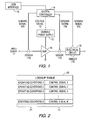
- the amplifier 10 receives an input signal 11 and outputs a signal to an electrical circuit 18 depicted simply as a block in Figure 1 for clarity purposes.
- the electrical circuit 18 can be any electrical circuit and preferentially represents an electrical circuit that would be in a television transmitter downstream of the power amplification stage.
- the electrical circuit 18 may contain amplifier stages in addition to the amplifier 10 depicted in Figure 1 .
- the electrical circuit 18 may include the amplifier 10.
- the variable power supply 12 supplies a voltage to the amplifier 10 in response to the control signal 13 from the system controller 14.
- the system controller 14 preferentially includes sensing means for sensing the operating conditions, as defined above, via sensors 17A, 17B, and 17C adapted to sense the operating conditions, of the input signal 11, the amplifier 10, and the electrical circuit 18. Sensors 17A, 17B, and 17C transmit sensing signal 15A, 15B, and 15C, respectively, to the sensing means in the system controller 14.
- the sensing means may also include a lookup table so that a control signal 13 can be sent to the variable power supply 12 so as to dynamically adjust the voltage being supplied by the variable power supply to the amplifier 10 as a function of the operating conditions sensed.
- the sensing means is comprised of known prior art components and circuitry for operating as described herein.
- the sensing means includes the sensors 17A and 17B for sensing the operating conditions of the circuit shown in Figure 1 .
- the sensing means includes a lookup table for determining the amount of amplification to be applied to the input signal 11 by the amplifier 10 as a function of the sensed operating conditions and for sending the control signal 13 to the variable power supply 12 thereby controlling the voltage level supplied by the variable power supply to the amplifier in response to one or more of the sensed operating conditions.
- the user interface 16 may be used to interface with the system controller 14 so that human interaction with the circuit depicted in Figure 1 is possible.
- the user interface 16 may be used to manually control the voltage supplied by the variable power supply 12 to the amplifier 10 either in response to one or more of the operating conditions or altogether independent of the operating conditions, as discussed above.
- the circuit shown in Figure 1 the input signal 11 is applied to an input terminal of the amplifier 10.
- the input signal 11 may be an 8VSB or COFDM signal as described herein.
- the sensors 17A, 17B, and 17C sense the operating conditions as described herein.
- the system controller 14, which comprises sensing means including a lookup table, as later described herein, accesses the lookup table to determine the characteristics of the control signal 13 based on one or more of the operating conditions.
- the system controller 14 sends a control signal 13 to the variable power supply 12, which is responsive to the particular characteristics of the control signal 13, such as voltage or current level, frequency, or phase, so as to dynamically control the voltage of the power supplied to the amplifier 10 as a function of one or more of the sensed operating condition or conditions.
- a lookup table 20 is depicted illustrating the indexing of the table by the operating conditions 22 so as to extract a control signal 13 for controlling the variable power supply 12 in any of Figures 1 , 3 , 4 , or 5 .
- the lookup table 20 is populated by collecting data on the performance of a test amplifier representative of the design of the amplifier 10 in response to input signals generated by an 8VSB or COFDM signal source where the test amplifier is connected to an instrumented test load. Similarly, the lookup table 20 is populated by collecting data on the performance of a test amplifier/test network system representative of the design of the amplifier 10 and the electrical circuit 18 in response to input signals of any modulation and of any frequency within the frequency range of the amplifier 10.
- the signal source may generate input signals such as the amplifier 11 may receive during the operation of the circuit in any of Figure 1 , 3 , 4 , or 5 .
- the test amplifier may be operated under a nominal supply voltage at a number of input signal frequencies in the expected operating range of the circuit in any of Figure 1 , 3 , 4 , or 5 while maintaining the required spectral containment, average output power, and amplifier efficiency and/or power dissipation.
- the test amplifier may then be operated at supply voltages above and below the nominal supply voltage.
- the results of these tests may be used to populate the lookup table 20 in Figure 2 .
- the lookup table is populated in conjunction with the description above, by collecting data from the actual operating circuit shown in Figure 1 by known techniques.
- FIG. 3 a second embodiment of the invention is shown where the amplifiers 10-1 through 10-N are arranged in a cascaded series.
- a plurality of amplifiers is contemplated in the cascaded series shown, such as two amplifiers, three amplifiers, etc.
- the variable power supply 12 is shown as supplying power to each of the cascaded amplifiers.
- the system controller 14, which preferentially comprises sensing means including a lookup table as described above, receives the sensing signals 15D and 15C.
- the sensing signal 15D may originate from one or more of the sensors 17N.
- sensing signal 15D may originate from any of the sensors 17N shown immediately preceding or following one of the cascaded amplifiers 10-1 through 10-N.
- Sensing signal 15C may originate from the sensor 17C sensing the operating conditions of the electrical circuit 18 as described above in the description of Figure 1 .
- an electrical circuit such as the electrical circuit 18 shown in the Figures, may be included after each or some of the amplifiers 10-1 through 10-N. Where there is more than one electrical circuit, the electrical circuits may all be the same, some of the electrical circuits may be the same as some other electrical circuits, or all of the electrical circuits may be different.
- the circuit shown in Figure 3 senses one or more of the operating conditions via one or more of sensors 17N and/or 17C and a sensing signal 15D and/or 15C, respectively, may be sent to the system controller 14.
- the system controller comprises a sensing means, as described above, including a lookup table.
- the lookup table determines the characteristics of the control signal 13 as a function of one or more of the operating conditions.
- the control signal 13 is sent from the system controller 14 to the variable power supply 12 so as to dynamically control the voltage of the power supplied to the amplifier 10 as a function of one or more of the sensed operating condition or conditions.
- the amplifiers 10-1 through 10-N are dynamically adjusted in concert as the variable power supply 12 is adjusted in response to one or more of the sensed operating conditions.
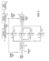
- FIG. 4 a third embodiment of the invention is shown where the amplifiers 10-1 through 10-N are arranged in a cascaded series.
- a plurality of amplifiers is contemplated in the cascaded series shown, such as two amplifiers, three amplifiers, etc.
- a one of variable power supply 12-1 through 12-N is associated with each one of the amplifiers 10-1 through 10-N, respectively, as shown.
- the system controller 14, which preferentially comprises sensing means including at least one lookup table as described above, receives the sensing signals 15D and 15C. As described above in the description of Figure 3 , the sensing signal 15D may originate from one or more of the sensors 17N.
- sensing signal 15D may originate from any of the sensors 17N shown immediately preceding or following one of the cascaded amplifiers 10-1 through 10-N.
- Sensing signal 15C may originate from the sensor 17C sensing the operating conditions of the electrical circuit 18 as described above in the description of Figure 3 .
- an electrical circuit such as the electrical circuit 18, may be placed after some or all of the amplifiers 10-1 through 10-N.
- the system controller 14 may send one or more of the control signals 13-1 through 13-N to the variable power supplies 12-1 through 12-N, respectively, so as to control the amplifiers 10-1 through 10-N in response to one or more of the sensed operating conditions.
- the system controller 14 includes sensing means, as described above, which may include one or more lookup tables and may include one lookup table for each of the variable power supply/amplifier combinations.
- the system controller 14 may be capable of controlling each of the variable power supplies 12-1 through 12-N separately, all together as one unit, or as multiple groups of varying numbers of amplifiers.
- the circuit shown in Figure 4 senses one or more of the operating conditions via one or more of sensors 17N and/or 17C and a sensing signal 15D and/or 15C, respectively, may be sent to the system controller 14.
- the system controller comprises a sensing means, as described above, including at least one lookup table. Any one of the lookup tables may determine the characteristics of a control signal 13-1 through 13-N as a function of one or more of the operating conditions.
- the control signals 13-1 through 13-N may be sent from the system controller 14 to one or more of the variable power supplies 12-1 through 12-N so as to dynamically control the voltage of the power supplied to one or more of the amplifiers 10-1 through 10-N as a function of one or more of the sensed operating condition or conditions.
- a fourth embodiment of the invention is shown where the amplifiers 10-1 through 10-N are arranged in a parallel cascade.
- a plurality of amplifiers is contemplated in the parallel cascade shown, such as two amplifiers, three amplifiers, etc.
- the variable power supply 12 is shown as supplying power to each of the parallel cascade of the amplifiers 10-1 through 10-N as shown. It is to be understood that the present invention also contemplates an individual variable power supply for each of the amplifiers 10-1 through 10-N, similar to the arrangement shown in the embodiment in Figure 4 .
- the embodiment with a plurality of variable power supply/amplifier pairs in a parallel cascade is not shown but may be inferred from this description.
- the system controller 14, which preferentially comprises sensing means including at least one lookup table as described above, receives the sensing signals 15E and 15C.
- the sensing signal 15E is analogous to the sensing signal 15D as described above in the description of Figure 3 .
- the sensing signal 15E may originate from one or more of the sensors 17N. Only two of the sensors 17N are connected to the system controller 14 for clarity and only one of the sensors 17N is labeled in Figure 5 for clarity, but it is to be understood that the sensing signal 15E may originate from any of the sensors 17N shown immediately preceding or following one of the parallel cascade amplifiers 10-1 through 10-N.
- Sensing signal 15C may originate from the sensor 17C sensing the operating conditions of the electrical circuit 18 as described above in the description of Figure 3 .
- the electrical circuit 18 may preferentially include a combiner (not shown for clarity) to combine the output signals from the amplifiers 10-1 through 10-N.
- the electrical circuit 18 may also include one or more of the amplifiers 10-1 through 10-N.
- the system controller 14 may send the control signal 13 to the variable power supply 12 so as to control the amplifiers 10-1 through 10-N in response to one or more of the sensed operating conditions.
- the system controller 14 includes sensing means, as described above, including a lookup table, the operation of which is as described above.
- the circuit shown in Figure 5 senses one or more of the operating conditions via one or more of sensors 17N and/or 17C and a sensing signal 15E and/or 15C, respectively, may be sent to the system controller 14.
- the system controller comprises a sensing means, as described above, including a lookup table.
- the lookup tables may determine the characteristics of the control signal 13 as a function of one or more of the operating conditions.
- the control signal 13 may be sent from the system controller 14 to the variable power supply 12 so as to dynamically control the voltage of the power supplied to one or more of the amplifiers 10-1 through 10-N as a function of one or more of the sensed operating condition or conditions.
- the present invention also contemplates an embodiment comprising a parallel cascade arrangement of amplifier/variable power supply combinations.
- the operation of this embodiment may be inferred from the description provided above for the embodiments shown in Figures 1 , 3 , 4 , and 5 .
Landscapes
- Engineering & Computer Science (AREA)
- Power Engineering (AREA)
- Amplifiers (AREA)
- Transmitters (AREA)
Abstract
Claims (6)
- Procédé de commande dynamique de la plage linéaire d'amplification appliquée par un amplificateur (10) dans un circuit électrique ayant une borne d'entrée pour recevoir un signal d'entrée (11) comprenant les étapes de :(a) prévision dudit circuit électrique ayant ladite borne d'entrée pour recevoir ledit signal d'entrée (11) et prévision dudit amplificateur (10) dans ledit circuit électrique ;(b) amplification du signal d'entrée (11) avec la plage linéaire d'amplification fixée comme une fonction d'une condition opérationnelle du circuit électrique (18) ;(c) application d'une tension variable audit amplificateur à partir d'une source d'alimentation électrique variable (12) pour ainsi commander la plage linéaire d'amplification appliquée par ledit amplificateur (10) audit signal d'entrée (11) ;(d) détection de ladite condition opérationnelle du circuit électrique (18) ;(e) peuplement d'une table de conversion (20) par (i) collecte de données sur la performance d'un circuit d'amplificateur test représentatif de la conception dudit amplificateur (10) dans ledit circuit électrique (18) lors de l'utilisation dudit amplificateur test pendant une collecte de données à diverses tensions et fréquences d'alimentation, tout en conservant le contenu spectral requis ; et par (ii) collecte de données sur la performance dudit amplificateur (10) à partir dudit circuit électrique (18) actuellement opérationnel ;(f) détermination à partir de ladite table de conversion (20) de la tension variable désirée appliquée audit amplificateur (10) comme une fonction de ladite condition opérationnelle ;(g) commande du niveau de ladite tension variable appliquée audit amplificateur (10) comme une fonction de ladite condition opérationnelle, commandant ainsi dynamiquement la plage linéaire d'amplification dudit amplificateur (10).
- Procédé selon la revendication 1, dans lequel ladite condition opérationnelle est choisie parmi le groupe consistant en la fréquence dudit signal d'entrée, l'impédance dudit circuit électrique, l'efficacité dudit amplificateur, la modulation dudit signal d'entrée, le rapport de la puissance de pic sur la puissance moyenne dudit signal d'entrée et le rapport de la tension de pic sur la tension moyenne dudit signal d'entrée.
- Procédé selon la revendication 1, dans lequel ledit signal d'entrée (11) est un signal COFDM ou un signal 8VSB.
- Procédé selon la revendication 1, dans lequel ledit signal d'entrée (11) est un signal 8VSB et dans lequel ladite condition opérationnelle est le rapport de la puissance de pic sur la puissance moyenne du signal d'entrée dans la plage de 5,0 à 8,0 dB.
- Procédé selon la revendication 1, dans lequel ledit signal d'entrée (11) est un signal COFDM et dans lequel ladite condition opérationnelle est le rapport de la puissance de pic sur la puissance moyenne du signal d'entrée dans la plage de 7 à 11 dB.
- Procédé selon la revendication 1, dans lequel ledit circuit électrique est un circuit d'émetteur de télévision.
Applications Claiming Priority (3)
| Application Number | Priority Date | Filing Date | Title |
|---|---|---|---|
| US931737 | 1992-08-18 | ||
| US09/931,737 US6683496B2 (en) | 2001-08-20 | 2001-08-20 | System and method for minimizing dissipation in RF power amplifiers |
| PCT/US2002/025349 WO2003017468A2 (fr) | 2001-08-20 | 2002-08-12 | Systeme et procede d'attenuation de la dissipation dans les amplificateurs de puissance rf |
Publications (3)
| Publication Number | Publication Date |
|---|---|
| EP1428313A2 EP1428313A2 (fr) | 2004-06-16 |
| EP1428313A4 EP1428313A4 (fr) | 2006-06-07 |
| EP1428313B1 true EP1428313B1 (fr) | 2010-07-14 |
Family
ID=25461265
Family Applications (1)
| Application Number | Title | Priority Date | Filing Date |
|---|---|---|---|
| EP02759314A Expired - Lifetime EP1428313B1 (fr) | 2001-08-20 | 2002-08-12 | Systeme et procede d'attenuation de la dissipation dans les amplificateurs de puissance rf |
Country Status (5)
| Country | Link |
|---|---|
| US (1) | US6683496B2 (fr) |
| EP (1) | EP1428313B1 (fr) |
| AU (1) | AU2002324657A1 (fr) |
| DE (1) | DE60237019D1 (fr) |
| WO (1) | WO2003017468A2 (fr) |
Families Citing this family (29)
| Publication number | Priority date | Publication date | Assignee | Title |
|---|---|---|---|---|
| US6734724B1 (en) * | 2000-10-06 | 2004-05-11 | Tropian, Inc. | Power control and modulation of switched-mode power amplifiers with one or more stages |
| EP1544996B1 (fr) * | 2002-07-29 | 2011-06-29 | Sharp Kabushiki Kaisha | Dispositif de reglage de volume, amplificateur numerique, et dispositif de reproduction de signaux numeriques |
| US7405617B2 (en) * | 2004-04-09 | 2008-07-29 | Skyworks Solutions, Inc. | Dynamic biasing system for an amplifier |
| US7190221B2 (en) * | 2004-10-22 | 2007-03-13 | Nokia Corporation | Method and apparatus for maintaining constant linearity for a power amplifier over varying load conditions |
| US7760024B2 (en) * | 2005-10-07 | 2010-07-20 | Cisco Technology, Inc | System and method for increasing accuracy of transmitter power detection over a larger range of output power levels |
| RU2434317C2 (ru) | 2006-05-05 | 2011-11-20 | Астриум Лимитед | Радиочастотные усилители мощности |
| US7826810B2 (en) | 2006-05-08 | 2010-11-02 | Harris Corporation | Multiband radio with transmitter output power optimization |
| US7768353B2 (en) * | 2008-06-13 | 2010-08-03 | Samsung Electro-Mechanics Company, Ltd. | Systems and methods for switching mode power amplifier control |
| CN101630944B (zh) * | 2008-07-17 | 2012-10-17 | 联咏科技股份有限公司 | 可提升反应速度的驱动电路 |
| TWI349425B (en) * | 2008-07-18 | 2011-09-21 | Novatek Microelectronics Corp | Driving circuit for enhancing response speed and related method |
| US8107903B2 (en) * | 2008-11-07 | 2012-01-31 | Triquint Semiconductor, Inc. | Radio frequency amplification circuit utilizing variable voltage generator |
| US7768346B1 (en) * | 2009-02-18 | 2010-08-03 | Atheros Communications, Inc. | System for amplifier linearization with envelope feedback |
| WO2011056729A2 (fr) | 2009-11-05 | 2011-05-12 | Rambus Inc. | Gestion d'horloge d'interface |
| KR101089955B1 (ko) * | 2009-12-28 | 2011-12-05 | 삼성전기주식회사 | 전력 증폭기 |
| JP5112464B2 (ja) * | 2010-03-17 | 2013-01-09 | 株式会社東芝 | 電力増幅装置、電力増幅方法 |
| GB201005404D0 (en) * | 2010-03-30 | 2010-05-12 | Nujira Ltd | Efficient amplification stage |
| US8819944B2 (en) * | 2010-06-07 | 2014-09-02 | Hyde Tools, Inc. | Bladed tool with a bent blade-retaining shank |
| CN101938258B (zh) * | 2010-08-27 | 2013-06-05 | 华为终端有限公司 | 一种控制射频功率放大器发射信号的方法和装置 |
| US8890616B2 (en) * | 2010-12-05 | 2014-11-18 | Rf Micro Devices (Cayman Islands), Ltd. | Power amplifier system with a current bias signal path |
| CN102571131B (zh) * | 2012-01-12 | 2017-02-15 | 中兴通讯股份有限公司 | 电源装置及其管理电源的方法和无线通信终端 |
| WO2013134026A2 (fr) | 2012-03-04 | 2013-09-12 | Quantance, Inc. | Système amplificateur de puissance à suivi d'enveloppe avec calibrage de retard |
| US9054916B1 (en) * | 2012-04-13 | 2015-06-09 | Rambus Inc. | Configurable receiver |
| TWI484752B (zh) | 2012-07-24 | 2015-05-11 | Orise Technology Co Ltd | 具增強迴轉率的單增益緩衝器 |
| EP3089371B1 (fr) | 2013-03-14 | 2017-10-18 | Quantance, Inc. | Système et avec réglage de bruit |
| US9270239B2 (en) * | 2013-03-15 | 2016-02-23 | Quantance, Inc. | Envelope tracking system with internal power amplifier characterization |
| US10431428B2 (en) | 2014-01-10 | 2019-10-01 | Reno Technologies, Inc. | System for providing variable capacitance |
| US9728378B2 (en) * | 2014-05-02 | 2017-08-08 | Reno Technologies, Inc. | Method for controlling an RF generator |
| KR102456842B1 (ko) * | 2016-12-08 | 2022-10-21 | 한국전자통신연구원 | 적응적 전원 전압을 인가함으로써 선형성과 효율성이 향상된 다단 증폭기 |
| US10509624B2 (en) * | 2017-01-30 | 2019-12-17 | Cirrus Logic, Inc. | Single-bit volume control |
Family Cites Families (13)
| Publication number | Priority date | Publication date | Assignee | Title |
|---|---|---|---|---|
| US4547746A (en) * | 1984-04-09 | 1985-10-15 | Rockwell International Corporation | VSWR Tolerant linear power amplifier |
| GB8828635D0 (en) * | 1988-12-08 | 1989-01-11 | Hewlett Packard Co | Rf amplifier bias circuit |
| US5081425A (en) | 1990-05-24 | 1992-01-14 | E-Systems, Inc. | Vswr adaptive power amplifier system |
| US5251331A (en) | 1992-03-13 | 1993-10-05 | Motorola, Inc. | High efficiency dual mode power amplifier apparatus |
| US5420536A (en) * | 1993-03-16 | 1995-05-30 | Victoria University Of Technology | Linearized power amplifier |
| US6137355A (en) * | 1994-04-17 | 2000-10-24 | Sevic; John F. | Dual-mode amplifier with high efficiency and high linearity |
| US5774017A (en) * | 1996-06-03 | 1998-06-30 | Anadigics, Inc. | Multiple-band amplifier |
| JPH1022756A (ja) * | 1996-07-04 | 1998-01-23 | Mitsubishi Electric Corp | 無線送信機およびその送信制御方法 |
| FR2758024B1 (fr) * | 1996-12-30 | 1999-01-29 | Alsthom Cge Alcatel | Dispositif d'alimentation d'un amplificateur de puissance pour terminal de radiocommunications mobiles |
| US5880635A (en) * | 1997-04-16 | 1999-03-09 | Sony Corporation | Apparatus for optimizing the performance of a power amplifier |
| KR100573988B1 (ko) * | 1997-12-12 | 2006-04-25 | 코닌클리케 필립스 일렉트로닉스 엔.브이. | 통신 장치 |
| US6166598A (en) * | 1999-07-22 | 2000-12-26 | Motorola, Inc. | Power amplifying circuit with supply adjust to control adjacent and alternate channel power |
| US6359504B1 (en) * | 2000-01-28 | 2002-03-19 | Lucent Technologies Inc. | Power amplifier using upstream signal information |
-
2001
- 2001-08-20 US US09/931,737 patent/US6683496B2/en not_active Expired - Lifetime
-
2002
- 2002-08-12 WO PCT/US2002/025349 patent/WO2003017468A2/fr not_active Application Discontinuation
- 2002-08-12 AU AU2002324657A patent/AU2002324657A1/en not_active Abandoned
- 2002-08-12 EP EP02759314A patent/EP1428313B1/fr not_active Expired - Lifetime
- 2002-08-12 DE DE60237019T patent/DE60237019D1/de not_active Expired - Lifetime
Also Published As
| Publication number | Publication date |
|---|---|
| US20030034839A1 (en) | 2003-02-20 |
| US6683496B2 (en) | 2004-01-27 |
| DE60237019D1 (de) | 2010-08-26 |
| WO2003017468A2 (fr) | 2003-02-27 |
| EP1428313A4 (fr) | 2006-06-07 |
| WO2003017468A3 (fr) | 2003-08-21 |
| EP1428313A2 (fr) | 2004-06-16 |
| AU2002324657A1 (en) | 2003-03-03 |
Similar Documents
| Publication | Publication Date | Title |
|---|---|---|
| EP1428313B1 (fr) | Systeme et procede d'attenuation de la dissipation dans les amplificateurs de puissance rf | |
| EP0734118B1 (fr) | Circuit de contrôle de la polarisation d'un amplificateur RF de puissance | |
| US5923215A (en) | Linearized amplifier | |
| US7512386B2 (en) | Method and apparatus providing integrated load matching using adaptive power amplifier compensation | |
| US7340227B2 (en) | Wireless communication system and semiconductor integrated circuit | |
| US7602243B2 (en) | Amplifier | |
| EP0482502B1 (fr) | Amplificateur de puissance et appareil radio mobile équipé d'un tel amplificateur | |
| US6831517B1 (en) | Bias-management system and method for programmable RF power amplifier | |
| JP3039613B2 (ja) | 増幅器 | |
| CN1118122A (zh) | 具有开关线性放大器的双工作方式传输系统 | |
| US20030030490A1 (en) | Distortion compensation amplification apparatus of feed forward type and adaptive pre-distortion type | |
| US6624700B2 (en) | Radio frequency power amplifier for cellular telephones | |
| US7061326B2 (en) | Transmission circuit capable of efficiently operating a power amplifier | |
| US7265627B2 (en) | Self adaptable bias circuit for enabling dynamic control of quiescent current in a linear power amplifier | |
| JP2000270032A (ja) | 電力制御回路および送信機 | |
| KR20090092074A (ko) | 무선 통신시스템의 전력 송신 장치 및 방법 | |
| US20060244533A1 (en) | Sliding bias circuit for enabling dynamic control of quiescent current in a linear power amplifier | |
| JPH0946264A (ja) | 線形変調無線送受信装置及びその電力制御方法 | |
| US8063513B2 (en) | Power source and method for controlling operational power | |
| AU769962B2 (en) | Transmitter for mobile terminal with carrier leak suppressing circuit | |
| GB2418792A (en) | An efficient mobile phone transmitter amplifier with an adapted power supply voltage | |
| WO2024195390A1 (fr) | Circuit amplificateur de puissance et procédé de commande de circuit amplificateur de puissance | |
| JPH1051243A (ja) | 増幅器 | |
| KR20020040400A (ko) | 가변 감쇠기 | |
| JPH08256018A (ja) | 高周波直線増幅器の消費電力制御回路 |
Legal Events
| Date | Code | Title | Description |
|---|---|---|---|
| PUAI | Public reference made under article 153(3) epc to a published international application that has entered the european phase |
Free format text: ORIGINAL CODE: 0009012 |
|
| 17P | Request for examination filed |
Effective date: 20040217 |
|
| AK | Designated contracting states |
Kind code of ref document: A2 Designated state(s): AT BE BG CH CY CZ DE DK EE ES FI FR GB GR IE IT LI LU MC NL PT SE SK TR |
|
| AX | Request for extension of the european patent |
Extension state: AL LT LV MK RO SI |
|
| A4 | Supplementary search report drawn up and despatched |
Effective date: 20060428 |
|
| 17Q | First examination report despatched |
Effective date: 20060811 |
|
| 17Q | First examination report despatched |
Effective date: 20060811 |
|
| GRAP | Despatch of communication of intention to grant a patent |
Free format text: ORIGINAL CODE: EPIDOSNIGR1 |
|
| RBV | Designated contracting states (corrected) |
Designated state(s): DE FR |
|
| GRAS | Grant fee paid |
Free format text: ORIGINAL CODE: EPIDOSNIGR3 |
|
| GRAA | (expected) grant |
Free format text: ORIGINAL CODE: 0009210 |
|
| AK | Designated contracting states |
Kind code of ref document: B1 Designated state(s): DE FR |
|
| REF | Corresponds to: |
Ref document number: 60237019 Country of ref document: DE Date of ref document: 20100826 Kind code of ref document: P |
|
| PLBE | No opposition filed within time limit |
Free format text: ORIGINAL CODE: 0009261 |
|
| REG | Reference to a national code |
Ref country code: FR Ref legal event code: ST Effective date: 20110502 |
|
| STAA | Information on the status of an ep patent application or granted ep patent |
Free format text: STATUS: NO OPPOSITION FILED WITHIN TIME LIMIT |
|
| 26N | No opposition filed |
Effective date: 20110415 |
|
| REG | Reference to a national code |
Ref country code: DE Ref legal event code: R097 Ref document number: 60237019 Country of ref document: DE Effective date: 20110415 |
|
| PG25 | Lapsed in a contracting state [announced via postgrant information from national office to epo] |
Ref country code: FR Free format text: LAPSE BECAUSE OF NON-PAYMENT OF DUE FEES Effective date: 20100914 |
|
| REG | Reference to a national code |
Ref country code: DE Ref legal event code: R082 Ref document number: 60237019 Country of ref document: DE Representative=s name: WUESTHOFF & WUESTHOFF PATENT- UND RECHTSANWAEL, DE |
|
| REG | Reference to a national code |
Ref country code: DE Ref legal event code: R081 Ref document number: 60237019 Country of ref document: DE Owner name: HBC SOLUTIONS, INC.(NACH DEN GES. DES STAATES , US Free format text: FORMER OWNER: HARRIS CORP., MELBOURNE, US Effective date: 20130508 Ref country code: DE Ref legal event code: R082 Ref document number: 60237019 Country of ref document: DE Representative=s name: WUESTHOFF & WUESTHOFF PATENT- UND RECHTSANWAEL, DE Effective date: 20130508 Ref country code: DE Ref legal event code: R081 Ref document number: 60237019 Country of ref document: DE Owner name: HBC SOLUTIONS, INC.(NACH DEN GES. DES STAATES , US Free format text: FORMER OWNER: HARRIS CORP., MELBOURNE, FLA., US Effective date: 20130508 Ref country code: DE Ref legal event code: R082 Ref document number: 60237019 Country of ref document: DE Representative=s name: WUESTHOFF & WUESTHOFF, PATENTANWAELTE PARTG MB, DE Effective date: 20130508 Ref country code: DE Ref legal event code: R081 Ref document number: 60237019 Country of ref document: DE Owner name: IMAGINE COMMUNICATIONS CORP., FRISCO, US Free format text: FORMER OWNER: HARRIS CORP., MELBOURNE, FLA., US Effective date: 20130508 |
|
| REG | Reference to a national code |
Ref country code: DE Ref legal event code: R082 Ref document number: 60237019 Country of ref document: DE Representative=s name: WUESTHOFF & WUESTHOFF, PATENTANWAELTE PARTG MB, DE Ref country code: DE Ref legal event code: R081 Ref document number: 60237019 Country of ref document: DE Owner name: IMAGINE COMMUNICATIONS CORP., FRISCO, US Free format text: FORMER OWNER: HBC SOLUTIONS, INC.(NACH DEN GES. DES STAATES DELAWARE), ENGLEWOOD, CO., US Ref country code: DE Ref legal event code: R081 Ref document number: 60237019 Country of ref document: DE Owner name: GATESAIR, INC., MASON, US Free format text: FORMER OWNER: HBC SOLUTIONS, INC.(NACH DEN GES. DES STAATES DELAWARE), ENGLEWOOD, CO., US |
|
| REG | Reference to a national code |
Ref country code: DE Ref legal event code: R082 Ref document number: 60237019 Country of ref document: DE Representative=s name: WUESTHOFF & WUESTHOFF, PATENTANWAELTE PARTG MB, DE Ref country code: DE Ref legal event code: R081 Ref document number: 60237019 Country of ref document: DE Owner name: GATESAIR, INC., MASON, US Free format text: FORMER OWNER: IMAGINE COMMUNICATIONS CORP., FRISCO, TEX., US |
|
| PGFP | Annual fee paid to national office [announced via postgrant information from national office to epo] |
Ref country code: DE Payment date: 20190828 Year of fee payment: 18 |
|
| REG | Reference to a national code |
Ref country code: DE Ref legal event code: R119 Ref document number: 60237019 Country of ref document: DE |
|
| PG25 | Lapsed in a contracting state [announced via postgrant information from national office to epo] |
Ref country code: DE Free format text: LAPSE BECAUSE OF NON-PAYMENT OF DUE FEES Effective date: 20210302 |