EP1424780A2 - Delta-Sigma Modulator, Verfahren zur Schaltung eines Delta-Sigma Modulators, und Digitalverstärker - Google Patents
Delta-Sigma Modulator, Verfahren zur Schaltung eines Delta-Sigma Modulators, und Digitalverstärker Download PDFInfo
- Publication number
- EP1424780A2 EP1424780A2 EP03257351A EP03257351A EP1424780A2 EP 1424780 A2 EP1424780 A2 EP 1424780A2 EP 03257351 A EP03257351 A EP 03257351A EP 03257351 A EP03257351 A EP 03257351A EP 1424780 A2 EP1424780 A2 EP 1424780A2
- Authority
- EP
- European Patent Office
- Prior art keywords
- delta
- sigma modulator
- filter coefficients
- bit rate
- volume setting
- Prior art date
- Legal status (The legal status is an assumption and is not a legal conclusion. Google has not performed a legal analysis and makes no representation as to the accuracy of the status listed.)
- Granted
Links
Images


Classifications
-
- H—ELECTRICITY
- H03—ELECTRONIC CIRCUITRY
- H03M—CODING; DECODING; CODE CONVERSION IN GENERAL
- H03M7/00—Conversion of a code where information is represented by a given sequence or number of digits to a code where the same, similar or subset of information is represented by a different sequence or number of digits
- H03M7/30—Compression; Expansion; Suppression of unnecessary data, e.g. redundancy reduction
- H03M7/3002—Conversion to or from differential modulation
- H03M7/3004—Digital delta-sigma modulation
- H03M7/3006—Compensating for, or preventing of, undesired influence of physical parameters
- H03M7/3011—Compensating for, or preventing of, undesired influence of physical parameters of non-linear distortion, e.g. by temporarily adapting the operation upon detection of instability conditions
-
- H—ELECTRICITY
- H03—ELECTRONIC CIRCUITRY
- H03M—CODING; DECODING; CODE CONVERSION IN GENERAL
- H03M7/00—Conversion of a code where information is represented by a given sequence or number of digits to a code where the same, similar or subset of information is represented by a different sequence or number of digits
- H03M7/30—Compression; Expansion; Suppression of unnecessary data, e.g. redundancy reduction
- H03M7/3002—Conversion to or from differential modulation
- H03M7/3004—Digital delta-sigma modulation
- H03M7/3015—Structural details of digital delta-sigma modulators
- H03M7/3031—Structural details of digital delta-sigma modulators characterised by the order of the loop filter, e.g. having a first order loop filter in the feedforward path
- H03M7/3033—Structural details of digital delta-sigma modulators characterised by the order of the loop filter, e.g. having a first order loop filter in the feedforward path the modulator having a higher order loop filter in the feedforward path, e.g. with distributed feedforward inputs
-
- H—ELECTRICITY
- H03—ELECTRONIC CIRCUITRY
- H03M—CODING; DECODING; CODE CONVERSION IN GENERAL
- H03M7/00—Conversion of a code where information is represented by a given sequence or number of digits to a code where the same, similar or subset of information is represented by a different sequence or number of digits
- H03M7/30—Compression; Expansion; Suppression of unnecessary data, e.g. redundancy reduction
- H03M7/3002—Conversion to or from differential modulation
- H03M7/3004—Digital delta-sigma modulation
- H03M7/3015—Structural details of digital delta-sigma modulators
- H03M7/3031—Structural details of digital delta-sigma modulators characterised by the order of the loop filter, e.g. having a first order loop filter in the feedforward path
- H03M7/3042—Structural details of digital delta-sigma modulators characterised by the order of the loop filter, e.g. having a first order loop filter in the feedforward path the modulator being of the error feedback type, i.e. having loop filter stages in the feedback path only
Definitions
- the present invention relates to a delta-sigma modulator, a method of switching a delta-sigma modulator, and a digital amplifier.
- a digital amplifier using delta-sigma modulation shifts quantization noise to a high-frequency band by noise shaping, to thereby secure the S/N ratio of an audio band.
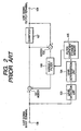
- Fig. 1 is a block diagram showing the configuration of a conventional quintic delta-sigma modulator.
- Noise shaping filter coefficients (a1, a2, a3, a4, a5) are fixed.
- the coefficients of the conventional delta-sigma modulator serving as a noise shaping filter used in a digital amplifier are fixed (e.g., see J.M. Goldberg and A.B. Sandler, "Noise Shaping and Pulse-Width Modulation for an All-Digital Audio Power Amplifier", Journal of the Audio Engineering Society, Vol. 39, No. 6, 1991.).
- the level of an m-bit input signal is detected by a level detection unit 103, and the result of determination by a level determination unit 104 is input to a filter coefficient storage memory 105.
- Filter coefficients that make the amplitude frequency properties of quantization noise coincide with auditory sensitivity properties changing in accordance with the level of the m-bit input signal is stored in advance in the filter coefficient storage memory 105.
- Properties of a variable filter 106 are determined by the filter coefficients selected in accordance with the level determined by the level determination unit 104, and a difference between the output of an adder 101 and an output signal of a quantizer 107 is input to the variable filter 106 and added to the m-bit input signal.
- the maximum amplitude of the input signal must be restricted when a high-order delta-sigma modulator is used in order to raise the S/N ratio.
- a high-order delta-sigma modulator it becomes necessary to raise the voltage at the power switching stage in order to obtain a predetermined output, which is a disadvantage in terms of performance and costs.
- a low-order delta-sigma modulator must be used in order to allow an input signal of a large amplitude, it is difficult to raise the S/N ratio.
- the delta-sigma modulator is configured so that an average value of the absolute value of the amplitude of the input signal in a past predetermined period of time is detected, the level of this value is determined, and switching is conducted by the level.
- a delta-sigma modulator shifts quantization noise of a digital audio signal to a high-frequency band to reduce noise of the band of the digital audio signal.
- the delta-sigma modulator includes a quantization bit rate detecting unit configured to detect a quantization bit rate of the digital audio signal, a volume setting value detecting unit configured to detect a volume setting value of the digital audio signal, a filtering unit configured to have plural sets of filter coefficients having different shaping properties and allow the quantization noise to pass, and a filter coefficient switching unit configured to switch the filter coefficients of the filtering unit in accordance with the detection result of the quantization bit rate detecting unit and the detection result of the volume setting value detecting unit.
- a method of switching a delta-sigma modulator includes detecting a quantization bit rate of a digital audio signal, detecting a volume setting value of the digital audio signal, and switching filter coefficients in accordance with the quantization bit rate and the volume setting value.
- a digital amplifier includes the delta-sigma modulator as described above.
- Fig. 3 is a functional block diagram of a digital amplifier using a delta-sigma modulator according to the embodiment of the invention.
- a digital amplifier 20 using the delta-sigma modulator includes: a digital interface 1 that acquires an input signal from a digital source such as a CD (Compact Disc) or a DVD (Digital Versatile Disc); an over-sampling circuit 2 that over-samples the input signal acquired from the digital source via the digital interface 1; a digital volume 3 that adjusts gain with respect to the input signal whose sampling frequency has been raised; a delta-sigma modulator 4 that reduces a quantization bit rate with respect to the gain-adjusted input signal; a PCM (Pulse Code Modulation)/PWM (Pulse Width Modulation) convertor 5 that converts a pulse code modulation signal obtained by the delta-sigma modulator 4 into a pulse width modulation signal; a power switch 6 that switches an unillustrated power source using the period of the pulse width modulation signal, amplifies the amplitude of the pulse width modulation signal and generates a current
- a digital interface 1 that acquires an
- a delta-sigma modulation circuit making up the delta-sigma modulator 4 according to the embodiment of the invention is shown in Fig. 4, and the basic configuration and operation thereof will be described.
- the delta-sigma modulation circuit includes an adder E, a filter and a quantizer.
- quantization noise Nq(z) is fed back to an input side via the filter H(z).
- a 6-bit output signal Y(z) is output.
- the filter H(z) is appropriately designed and, as shown in the noise shaping property graph shown in Fig. 5, the quantization noise is shifted to a high-frequency band, whereby the noise of the audio band is reduced and the S/N ratio is secured.
- the delta-sigma modulator 4 according to the embodiment of the invention is configured as shown in Fig. 6 using a quintic delta-sigma modulation circuit (e.g., the circuit shown in Fig. 4).
- the delta-sigma modulator 4 includes a quantization bit rate detection unit 9 that detects the quantization bit rate of a digital audio signal that is the input source; a volume setting value detection unit 10 that detects a volume setting value of the digital audio signal; a filter 11 that includes plural sets of filter coefficients having different shaping properties and allows the quantization noise to pass; and a filter coefficient switcher 17 that switches the filter coefficients of gain adjustors 12 to 16 of the filter 11 in accordance with the bit rate and the volume setting value of the digital audio signal.
- a quantization bit rate detection unit 9 that detects the quantization bit rate of a digital audio signal that is the input source
- a volume setting value detection unit 10 that detects a volume setting value of the digital audio signal
- a filter 11 that includes plural sets of filter coefficients having different shaping properties and allows the quantization noise to pass
- a filter coefficient switcher 17 that switches the filter coefficients of gain adjustors 12 to 16 of the filter 11 in accordance with the bit rate and the volume setting value of the digital audio signal.
- the delta-sigma modulator 4 includes a quintic delta-sigma modulation circuit, the number of coefficients for each of delta-sigma conversion circuits is five. Additionally, the delta-sigma modulator 4 is characterized in that it plurally has filter coefficients where the five coefficients are used as one set.
- the delta-sigma modulator 4 has two sets of filter coefficients: quintic (high-order) filter coefficients (a1, a2, a3, a4, a5) and tertiary (low-order) filter coefficients (b1, b2, b3, 0, 0).
- quintic (high-order) filter coefficients a1, a2, a3, a4, a5
- tertiary (low-order) filter coefficients b1, b2, b3, 0, 0.
- Quintic filter coefficients (-5, 10, -10, 5, -1)
- Tertiary filter coefficients (-3, 3, -1, 0, 0)
- the filter coefficient switcher 17 always switches the filter coefficients to the tertiary filter coefficient set (b1, b2, b3, 0, 0) in the case of a source having a low quantization bit rate such as a CD, and in principle switches the filter coefficients to the quintic filter coefficients (a1, a2, a3, a4, a5) in the case of a source having a high quantization bit rate such as a DVD.
- the tertiary filter coefficients are used in a case where the volume setting value is set higher than a threshold value, which is lower than the maximum value thereof by a predetermined value, even in the case of a source with a high quantization bit rate.
- the filter coefficients are switched from quintic (high-order) to tertiary (low-order) when the volume setting value that had been set lower than the predetermined threshold value is changed to a value higher than the threshold value.
- the filter coefficients are switched from tertiary (low-order) to quintic (high-order) when the volume setting value that had been set higher than the predetermined threshold is changed to a value lower than the threshold.
- the threshold shown in Figs. 7 and 8 is preferably about -6 dB. The reason for this is because oscillation occurs when the input amplitude is not held to about 60% or less of the maximum value of the volume setting value with the quintic filter coefficients.
- the filter coefficient switcher 17 resets memories 18 to 22 storing the quantization noise to zero.
- the reason for this is to prevent the quantization noise from being excessively fed back when the filter coefficients are switched from the tertiary filter coefficient set to the quintic filter coefficient set, because the numerical values of the quintic filter coefficients are larger than those of the tertiary filter coefficients, as in the specific example of the numerical values mentioned above.
- the filter coefficients are switched from quintic (high-order) to tertiary (low-order) near the point in time when the rising starts.
- the filter coefficients are switched from tertiary (low-order) to quintic (high-order) near the point in time when the falling ends.
- the high-order filter coefficient set is always used with a volume setting value that is lower than the threshold (predetermined value).
- the system can be prevented from becoming unstable.
- the digital volume 3 After the over-sampling circuit 2 has raised the sampling frequency of the input signal from a digital source such as a CD or a DVD acquired via the digital interface 1, the digital volume 3 adjusts the gain.
- the delta-sigma modulator 4 reduces the quantization bit rate of the gain-adjusted input signal.
- the pulse code modulation signal obtained by the delta-sigma modulator 4 has been converted into the pulse width modulation signal by the PCM/PWM converter 5
- the unillustrated power source is switched by the power switch 6 using the period of the pulse width modulation signal
- the amplitude of the pulse width modulation signal is amplified, and the current applied to the speaker 8 is generated.
- the current is applied to the speaker 8.
- the filter coefficients are switched to the tertiary filter coefficient set in the case of a source whose input signal has a low quantization bit rate and switched to the quintic filter coefficient set in the case of a source having a high quantization bit rate.
- the filter coefficients are switched from quintic to tertiary when the volume setting value of the digital volume 3 has been changed to a value of about 50% or more of the maximum value thereof.
- the memories storing the quantization noise are reset to zero when the filter coefficients are switched from tertiary to quintic.
- the delta-sigma modulator 4 detects the quantization bit rate of the input signal (quantization bit rate detection step), switches the filter coefficients to the tertiary filter coefficient set in the case of a source having a low quantization bit rate, and switches the filter coefficients to the quintic filter coefficient set in the case of a source having a high quantization bit rate (filter coefficient switching step).
- quantization bit rate detection step switches the filter coefficients to the tertiary filter coefficient set in the case of a source having a low quantization bit rate
- filter coefficient switching step the S/N ratio that the source has can be secured even with a tertiary delta-sigma modulator, and the system does not become unstable even if the amplitude of the input signal becomes large.
- the S/N ratio can be set high by the delta-sigma modulator 4 operating as a quintic delta-sigma modulator
- the delta-sigma modulator 4 detects the volume setting value (volume setting detecting step) and switches the filter coefficients from quintic to tertiary when the value thereof has been changed to a high value of 50% or more of the maximum value (filter coefficient switching step).
- volume setting detecting step detects the volume setting value
- filter coefficient switching step switches the filter coefficients from quintic to tertiary when the value thereof has been changed to a high value of 50% or more of the maximum value.
- the memories storing the quantization noise are reset to zero when the filter coefficients are switched to the high-order coefficients.
- the quantization noise can be prevented from being excessively fed back even when the filter coefficients are switched from the tertiary filter coefficient set to the quintic filter coefficient set.
- the delta-sigma modulation circuit there are the circuits shown in Figs. 9 and 10.
- the delta-sigma modulation circuits shown in these diagrams not only the quantization noise but the signal have transfer functions.
- filter coefficient switching can also be applied to delta-sigma modulation circuits of such configurations as in the delta-sigma modulator according to the present embodiment.
- the delta-sigma modulator is a delta-sigma modulator that shifts quantization noise of a digital audio signal to a high-frequency band to thereby reduce noise of a band of the digital audio signal.
- the delta-sigma modulator includes the quantization bit rate detection unit 9 that detects the quantization bit rate of the digital audio signal; the volume setting value detection unit 10 that detects the volume setting value of the digital audio signal; the filter 11 that includes plural sets of filter coefficients having different shaping properties and allows the quantization noise to pass; and the filter coefficient switcher 17 that switches the filter coefficients of the filter 11 in accordance with the detection result of the quantization bit rate detection unit 9 and the detection result of the volume setting value detection unit 10.
- the delta-sigma modulator can switch the filter coefficients of the filter 11 in accordance with the detected value of the quantization bit rate of the input signal and the volume setting value.
- the delta-sigma modulator can switch the filter coefficients to the low-order coefficient set in the case of an input signal having a low quantization bit rate and can switch the filter coefficients to the high-order coefficient set in the case of an input signal having a high quantization bit rate.
- the system does not become unstable even if the amplitude of the input signal becomes large.
- the S/N ratio can be set high because the delta-sigma modulator operates as a high-order delta-sigma modulator.
- the method of switching the delta-sigma modulator includes the quantization bit rate detecting step that detects the quantization bit rate of a digital audio signal; the volume setting detecting step that detects the volume setting value of the digital audio signal; and the filter coefficient switching step that switches the filter coefficients in accordance with the quantization bit rate and the volume setting value.
- the filter coefficients can be switched to the low-order coefficient set in the case of an input signal having a low quantization bit rate
- the filter coefficients can be switched to the high-order coefficient set in the case of an input signal having a high quantization bit rate.
- the system can be prevented from becoming unstable even if the amplitude of the input signal becomes large.
- the S/N ratio can be set high.
- the digital amplifier according to the present embodiment includes the delta-sigma modulator of the present embodiment, a balance between a high S/N ratio and stability can be achieved.
Applications Claiming Priority (2)
| Application Number | Priority Date | Filing Date | Title |
|---|---|---|---|
| JP2002340745 | 2002-11-25 | ||
| JP2002340745A JP3902120B2 (ja) | 2002-11-25 | 2002-11-25 | デルタシグマ変調器およびディジタルアンプ |
Publications (3)
| Publication Number | Publication Date |
|---|---|
| EP1424780A2 true EP1424780A2 (de) | 2004-06-02 |
| EP1424780A3 EP1424780A3 (de) | 2005-01-19 |
| EP1424780B1 EP1424780B1 (de) | 2006-10-11 |
Family
ID=32290392
Family Applications (1)
| Application Number | Title | Priority Date | Filing Date |
|---|---|---|---|
| EP03257351A Expired - Fee Related EP1424780B1 (de) | 2002-11-25 | 2003-11-21 | Delta-Sigma Modulator, Verfahren zur Schaltung eines Delta-Sigma Modulators, und Digitalverstärker |
Country Status (4)
| Country | Link |
|---|---|
| US (1) | US20040122544A1 (de) |
| EP (1) | EP1424780B1 (de) |
| JP (1) | JP3902120B2 (de) |
| DE (1) | DE60308983T2 (de) |
Families Citing this family (5)
| Publication number | Priority date | Publication date | Assignee | Title |
|---|---|---|---|---|
| JP2006054545A (ja) * | 2004-08-10 | 2006-02-23 | Matsushita Electric Ind Co Ltd | ディジタルゲイン制御装置とそれを用いたオーディオ信号電力増幅装置、並びにそれらの方法 |
| KR101572121B1 (ko) | 2014-10-10 | 2015-11-26 | 이재석 | 저전압 직류전원을 이용한 발광 다이오드 조명제어 시스템 및 발광 다이오드 조명제어 방법 |
| CN105450199B (zh) * | 2015-11-19 | 2019-02-22 | 厦门大学 | 具有快速建立时间的级联积分梳状滤波器及其设计方法 |
| US9985646B1 (en) | 2017-10-18 | 2018-05-29 | Schweitzer Engineering Laboratories, Inc. | Analog-to-digital converter verification using quantization noise properties |
| US10033400B1 (en) | 2017-10-18 | 2018-07-24 | Schweitzer Engineering Laboratories, Inc. | Analog-to-digital converter verification using quantization noise properties |
Citations (6)
| Publication number | Priority date | Publication date | Assignee | Title |
|---|---|---|---|---|
| EP0512687A2 (de) * | 1991-04-09 | 1992-11-11 | Nokia Mobile Phones Ltd. | Modulator, insbesondere Sigma Delta Modulator |
| US5742246A (en) * | 1996-03-22 | 1998-04-21 | National Science Council | Stabilizing mechanism for sigma-delta modulator |
| US5757301A (en) * | 1997-05-01 | 1998-05-26 | National Science Council | Instability recovery method for sigma-delta modulators |
| US5959562A (en) * | 1997-09-03 | 1999-09-28 | Analog Devices, Inc. | Sigma-delta modulator and method for operating such modulator |
| US6064326A (en) * | 1998-03-30 | 2000-05-16 | Silicon Laboratories, Inc. | Analog-to-digital conversion overload detection and suppression |
| EP1130786A2 (de) * | 2000-02-18 | 2001-09-05 | Sony Corporation | Digitale Signalverarbeitungsvorrichtung und -verfahren und Delta-Sigma Modulator welcher dieses Verfahren anwendet |
Family Cites Families (2)
| Publication number | Priority date | Publication date | Assignee | Title |
|---|---|---|---|---|
| US5012244A (en) * | 1989-10-27 | 1991-04-30 | Crystal Semiconductor Corporation | Delta-sigma modulator with oscillation detect and reset circuit |
| EP1202461B1 (de) * | 2000-10-25 | 2005-03-09 | STMicroelectronics S.r.l. | Verfahren zur Verbesserung des Signal/Rausch-Verhältnisses eines Sigma/Delta-Modulators und dieses Verfahren benutzender Schaltkreis |
-
2002
- 2002-11-25 JP JP2002340745A patent/JP3902120B2/ja not_active Expired - Fee Related
-
2003
- 2003-11-20 US US10/716,508 patent/US20040122544A1/en not_active Abandoned
- 2003-11-21 DE DE60308983T patent/DE60308983T2/de not_active Expired - Fee Related
- 2003-11-21 EP EP03257351A patent/EP1424780B1/de not_active Expired - Fee Related
Patent Citations (6)
| Publication number | Priority date | Publication date | Assignee | Title |
|---|---|---|---|---|
| EP0512687A2 (de) * | 1991-04-09 | 1992-11-11 | Nokia Mobile Phones Ltd. | Modulator, insbesondere Sigma Delta Modulator |
| US5742246A (en) * | 1996-03-22 | 1998-04-21 | National Science Council | Stabilizing mechanism for sigma-delta modulator |
| US5757301A (en) * | 1997-05-01 | 1998-05-26 | National Science Council | Instability recovery method for sigma-delta modulators |
| US5959562A (en) * | 1997-09-03 | 1999-09-28 | Analog Devices, Inc. | Sigma-delta modulator and method for operating such modulator |
| US6064326A (en) * | 1998-03-30 | 2000-05-16 | Silicon Laboratories, Inc. | Analog-to-digital conversion overload detection and suppression |
| EP1130786A2 (de) * | 2000-02-18 | 2001-09-05 | Sony Corporation | Digitale Signalverarbeitungsvorrichtung und -verfahren und Delta-Sigma Modulator welcher dieses Verfahren anwendet |
Also Published As
| Publication number | Publication date |
|---|---|
| DE60308983D1 (de) | 2006-11-23 |
| US20040122544A1 (en) | 2004-06-24 |
| JP3902120B2 (ja) | 2007-04-04 |
| JP2004179739A (ja) | 2004-06-24 |
| DE60308983T2 (de) | 2007-03-08 |
| EP1424780A3 (de) | 2005-01-19 |
| EP1424780B1 (de) | 2006-10-11 |
Similar Documents
| Publication | Publication Date | Title |
|---|---|---|
| US6140875A (en) | Device for amplifying digital signals | |
| US7928876B2 (en) | Sigma delta modulator | |
| US7061416B2 (en) | Adaptive-type sigma-delta A/D converter | |
| US7148829B2 (en) | Delta-sigma modulation circuit with gain control function | |
| US5757299A (en) | Analog-Digital converter using delta sigma modulation digital filtering, and gain-scaling | |
| JP3369503B2 (ja) | ディジタルスイッチングアンプ | |
| US6822594B1 (en) | Overload protection and stability for high order 1-bit delta-sigma modulators | |
| US20050200405A1 (en) | Audio signal amplification method and apparatus | |
| JP2009531932A (ja) | デジタル信号コンバータ | |
| JP2004508598A (ja) | オーディオ信号圧縮 | |
| KR100497702B1 (ko) | 디지털데이터변환장치 | |
| JP3214981B2 (ja) | Agc機能付きデルタシグマ型a/d変換器 | |
| US20030058038A1 (en) | Class D amplifier | |
| EP1424780B1 (de) | Delta-Sigma Modulator, Verfahren zur Schaltung eines Delta-Sigma Modulators, und Digitalverstärker | |
| JP2006295769A (ja) | スイッチング増幅器 | |
| US20080174362A1 (en) | Voltage supply circuit and circuit device | |
| GB2437414A (en) | Sigma-delta modulator | |
| JP4617298B2 (ja) | クリップ検出と信号変調システム及び方法 | |
| JP4148077B2 (ja) | D級信号増幅回路 | |
| US7999712B2 (en) | Digital-to-analog converters and methods thereof | |
| EP2555423B1 (de) | Digitaler verstärker | |
| JP2822734B2 (ja) | ノイズシェイパ | |
| EP1293036B1 (de) | Demodulationsfilter | |
| KR20010043852A (ko) | 변환기 | |
| JP4641282B2 (ja) | Δς変調回路、及びその発振防止方法 |
Legal Events
| Date | Code | Title | Description |
|---|---|---|---|
| PUAI | Public reference made under article 153(3) epc to a published international application that has entered the european phase |
Free format text: ORIGINAL CODE: 0009012 |
|
| AK | Designated contracting states |
Kind code of ref document: A2 Designated state(s): AT BE BG CH CY CZ DE DK EE ES FI FR GB GR HU IE IT LI LU MC NL PT RO SE SI SK TR |
|
| AX | Request for extension of the european patent |
Extension state: AL LT LV MK |
|
| PUAL | Search report despatched |
Free format text: ORIGINAL CODE: 0009013 |
|
| AK | Designated contracting states |
Kind code of ref document: A3 Designated state(s): AT BE BG CH CY CZ DE DK EE ES FI FR GB GR HU IE IT LI LU MC NL PT RO SE SI SK TR |
|
| AX | Request for extension of the european patent |
Extension state: AL LT LV MK |
|
| 17P | Request for examination filed |
Effective date: 20050225 |
|
| AKX | Designation fees paid |
Designated state(s): DE FR GB |
|
| GRAP | Despatch of communication of intention to grant a patent |
Free format text: ORIGINAL CODE: EPIDOSNIGR1 |
|
| GRAS | Grant fee paid |
Free format text: ORIGINAL CODE: EPIDOSNIGR3 |
|
| GRAA | (expected) grant |
Free format text: ORIGINAL CODE: 0009210 |
|
| AK | Designated contracting states |
Kind code of ref document: B1 Designated state(s): DE FR GB |
|
| REG | Reference to a national code |
Ref country code: GB Ref legal event code: FG4D |
|
| REF | Corresponds to: |
Ref document number: 60308983 Country of ref document: DE Date of ref document: 20061123 Kind code of ref document: P |
|
| ET | Fr: translation filed | ||
| PLBE | No opposition filed within time limit |
Free format text: ORIGINAL CODE: 0009261 |
|
| STAA | Information on the status of an ep patent application or granted ep patent |
Free format text: STATUS: NO OPPOSITION FILED WITHIN TIME LIMIT |
|
| 26N | No opposition filed |
Effective date: 20070712 |
|
| PGFP | Annual fee paid to national office [announced via postgrant information from national office to epo] |
Ref country code: DE Payment date: 20071115 Year of fee payment: 5 |
|
| PGFP | Annual fee paid to national office [announced via postgrant information from national office to epo] |
Ref country code: FR Payment date: 20071108 Year of fee payment: 5 Ref country code: GB Payment date: 20071121 Year of fee payment: 5 |
|
| GBPC | Gb: european patent ceased through non-payment of renewal fee |
Effective date: 20081121 |
|
| REG | Reference to a national code |
Ref country code: FR Ref legal event code: ST Effective date: 20090731 |
|
| PG25 | Lapsed in a contracting state [announced via postgrant information from national office to epo] |
Ref country code: DE Free format text: LAPSE BECAUSE OF NON-PAYMENT OF DUE FEES Effective date: 20090603 |
|
| PG25 | Lapsed in a contracting state [announced via postgrant information from national office to epo] |
Ref country code: GB Free format text: LAPSE BECAUSE OF NON-PAYMENT OF DUE FEES Effective date: 20081121 |
|
| PG25 | Lapsed in a contracting state [announced via postgrant information from national office to epo] |
Ref country code: FR Free format text: LAPSE BECAUSE OF NON-PAYMENT OF DUE FEES Effective date: 20081130 |