EP1424725A1 - ELECTRODE FOR p-TYPE SiC - Google Patents
ELECTRODE FOR p-TYPE SiC Download PDFInfo
- Publication number
- EP1424725A1 EP1424725A1 EP02760799A EP02760799A EP1424725A1 EP 1424725 A1 EP1424725 A1 EP 1424725A1 EP 02760799 A EP02760799 A EP 02760799A EP 02760799 A EP02760799 A EP 02760799A EP 1424725 A1 EP1424725 A1 EP 1424725A1
- Authority
- EP
- European Patent Office
- Prior art keywords
- electrode
- layer
- type sic
- electrode material
- sic
- Prior art date
- Legal status (The legal status is an assumption and is not a legal conclusion. Google has not performed a legal analysis and makes no representation as to the accuracy of the status listed.)
- Withdrawn
Links
Images




Classifications
-
- H—ELECTRICITY
- H10—SEMICONDUCTOR DEVICES; ELECTRIC SOLID-STATE DEVICES NOT OTHERWISE PROVIDED FOR
- H10D—INORGANIC ELECTRIC SEMICONDUCTOR DEVICES
- H10D64/00—Electrodes of devices having potential barriers
- H10D64/60—Electrodes characterised by their materials
- H10D64/62—Electrodes ohmically coupled to a semiconductor
-
- H—ELECTRICITY
- H10—SEMICONDUCTOR DEVICES; ELECTRIC SOLID-STATE DEVICES NOT OTHERWISE PROVIDED FOR
- H10D—INORGANIC ELECTRIC SEMICONDUCTOR DEVICES
- H10D64/00—Electrodes of devices having potential barriers
- H10D64/01—Manufacture or treatment
- H10D64/011—Manufacture or treatment of electrodes ohmically coupled to a semiconductor
-
- H—ELECTRICITY
- H10—SEMICONDUCTOR DEVICES; ELECTRIC SOLID-STATE DEVICES NOT OTHERWISE PROVIDED FOR
- H10D—INORGANIC ELECTRIC SEMICONDUCTOR DEVICES
- H10D62/00—Semiconductor bodies, or regions thereof, of devices having potential barriers
- H10D62/80—Semiconductor bodies, or regions thereof, of devices having potential barriers characterised by the materials
- H10D62/83—Semiconductor bodies, or regions thereof, of devices having potential barriers characterised by the materials being Group IV materials, e.g. B-doped Si or undoped Ge
- H10D62/832—Semiconductor bodies, or regions thereof, of devices having potential barriers characterised by the materials being Group IV materials, e.g. B-doped Si or undoped Ge being Group IV materials comprising two or more elements, e.g. SiGe
- H10D62/8325—Silicon carbide
-
- H—ELECTRICITY
- H10—SEMICONDUCTOR DEVICES; ELECTRIC SOLID-STATE DEVICES NOT OTHERWISE PROVIDED FOR
- H10H—INORGANIC LIGHT-EMITTING SEMICONDUCTOR DEVICES HAVING POTENTIAL BARRIERS
- H10H20/00—Individual inorganic light-emitting semiconductor devices having potential barriers, e.g. light-emitting diodes [LED]
- H10H20/80—Constructional details
- H10H20/81—Bodies
- H10H20/822—Materials of the light-emitting regions
- H10H20/826—Materials of the light-emitting regions comprising only Group IV materials
-
- H—ELECTRICITY
- H10—SEMICONDUCTOR DEVICES; ELECTRIC SOLID-STATE DEVICES NOT OTHERWISE PROVIDED FOR
- H10H—INORGANIC LIGHT-EMITTING SEMICONDUCTOR DEVICES HAVING POTENTIAL BARRIERS
- H10H20/00—Individual inorganic light-emitting semiconductor devices having potential barriers, e.g. light-emitting diodes [LED]
- H10H20/80—Constructional details
- H10H20/83—Electrodes
- H10H20/832—Electrodes characterised by their material
Definitions
- This invention relates to a silicon carbide (SiC) device, and more particularly to an electrode for p-type SiC, which is employed in an SiC device.
- the p-electrode for the SiC device i.e. an ohmic electrode for p-type SiC is generally formed of TiAl composed of titanium (Ti) and aluminum (Al) (see JP-A-5-13812).
- the device needs an ohmic electrode.
- an ohmic contact between a semiconductor layer and an electrode cannot be obtained without being subjected to heat treatment. Only provision of a metallic layer exhibits a Schottky barrier.
- the ohmic contact formed by the heat treatment provides greatly different contact resistances according to a semiconductor material, an electrode material, a heat treatment temperature, a heat treatment time, etc.
- TiAl which is presently expected as a material for a low resistance ohmic contact, can provides very low resistance.
- heat treatment at a high temperature for a long time as well as a large amount of Al is required. This leads to the problems of deterioration of a device function, a device life, etc. due to deterioration of surface morphology and thermal damage for a semiconductor crystal layer.
- This invention has been accomplished in order to attain the above problems, and an object of this invention is to provide an electrode for p-type SiC which can provide improved surface morphology and less thermal damage for a semiconductor crystal layer due to formation of an electrode.
- An electrode for p-type SiC contains a first electrode material of at least one selected from the group consisting of nickel (Ni), cobalt (Co), palladium (Pd) and platinum (Pt).
- the electrode for p-type SiC having the above configuration can provide an ohmic property and improved flatness of the electrode surface by the heat treatment at a lower temperature than before.
- the above electrode for p-type SiC provides the ohmic property through the heat treatment in a wide range, for example by that for a short time at a high temperature. This reduces the thermal affect on the semiconductor crystal layer due to the formation of the electrode.
- an SiC device with an excellent device performance can be manufactured.
- the electrode for p-type SiC refers to the electrode formed on a p-type SiC semiconductor layer.
- the type of the p-type SiC semiconductor to which the electrode for p-type SiC according to this invention is applied should not be particularly limited, but includes 6H type, 15R type, 21R type, 3C type, etc. as well as the 4H type which is adopted in the embodiment described later.
- the kind of the device to which the electrode for p-type SiC according to this invention is applied should not be particularly limited, but may be various devices which are employed in a high frequency power device, a high temperature device, an optoelectronics device, etc.
- nickel or cobalt is particularly preferable because nickel or cobalt reacts with Si at a relatively low temperature.
- the electrode for p-type SiC according to this invention preferably further contains the second electrode material of aluminum (Al) in addition to the first electrode material.
- the containing of Al reduces the contact resistivity and provides the electrode for p-type SiC with an excellent ohmic property.
- the electrode for p-type SiC according to this invention preferably further contains the third electrode material of titanium (Ti).
- the electrode preferably contains the first electrode material of e.g. nickel (Ni), second electrode material of aluminum (Al), and third electrode material of titanium (Ti).
- the containing of the third electrode material of titanium (Ti) further reduces the contact resistivity.
- the electrode for p-type SiC according to this invention preferably includes a layer of the first electrode material (hereinafter referred to as a first electrode material layer). More preferably, the first electrode material layer is formed in contact with the p-type SiC semiconductor layer. For example, by forming the first electrode material layer on the p-type SiC semiconductor layer, subsequently stacking the layer of the other electrode material thereon and heat-treating these layers, the electrode for p-type SiC according to this invention can be manufactured.
- the electrode for p-type SiC contains the second electrode material as well as the first electrode material
- the electrode for p-type SiC according to this invention preferably includes the first electrode material layer and a layer of the second electrode material (hereinafter referred to as a second electrode material layer).
- the first electrode material layer and the second electrode material layer are preferably formed.
- the order of stacking the first material layer and the second material layer should not be particularly limited, but the first electrode material layer and the second electrode material layer are preferably stacked in order from the side of the p-type SiC semiconductor layer.
- the first electrode material layer is preferably formed in contact with the p-type semiconductor layer.
- a layer of the other material may be located between the first electrode material layer and the second electrode material layer.
- a plurality of layers of the first electrode material layer and/or the second electrode material layer may be formed.
- the first electrode material layer, the second electrode material layer and the first electrode material layer may be stacked in order from the side of the p-type SiC semiconductor layer to constitute the electrode for p-type SiC according to this invention.
- the electrode for p-type SiC contains the first electrode material, second electrode material and third electrode material
- the electrode for p-type SiC according to this invention preferably includes the first electrode material layer, second electrode material layer and a layer of the third electrode material (hereinafter referred to as a third electrode material layer).
- the first electrode material layer, second electrode material layer and third electrode material layer are preferably formed.
- the order of stacking these layers should not be particularly limited, but the first electrode material layer, third electrode material layer and second electrode material layer are preferably stacked in order from the side of the p-type SiC semiconductor layer.
- the first electrode material layer is preferably formed in contact with the p-type semiconductor layer.
- a layer of the other material may be located between the first electrode material layer and the third electrode material layer, and/or between the third electrode material layer and the second electrode material layer.
- a plurality of layers of the first electrode material layer, third electrode material layer and/or the second electrode material layer may be formed.
- the method of forming the first, the second and the third electrode layer should not be limited, but can be implemented by molecular beam epitaxy (MBE), sputtering, resistive heating, etc.
- MBE molecular beam epitaxy
- sputtering sputtering
- resistive heating etc.
- the electrode for p-type SiC according to this invention is manufactured by stacking the above electrode material layer (and other layers) on the p-type SiC semiconductor layer and thereafter heat-treating these layers.
- the p-type SiC semiconductor Prior to forming the electrode material layer, the p-type SiC semiconductor is preferably washed (e.g. chemically washed). This intends to stack the electrode materials in a desired state.
- the heat-treatment for the p-type SiC is carried out in order to form the ohmic contact between the p-type SiC semiconductor layer and the electrode for p-type SiC according to this invention.
- the heating temperature and the heating time are adjusted as required to provide an improved ohmic contact.
- the heating temperature may be e.g.
- the heating time may be e.g. 2 min. - 100 min., preferably 2 min. - 50 min. and more preferably 5 min. - 30 min.
- the heating is preferably carried out in a vacuum state.
- the heating can be carried out in an atmosphere of inert gas.
- the inert gas may be nitrogen gas, helium gas, argon gas, etc.
- a p-type 4H-SiC(0001) epitaxial wafer (Al concentration: 6.4 - 9.0 x 10 18 cm -3 ), which is commercially available was adopted.
- a thermal oxide film having a thickness of 10 nm was deposited thereon, and a circular TLM pattern was made by photolithography.
- Ni and Al were deposited by techniques of electron beam and resistive heating. Contact materials were made with their different thicknesses.
- heat treatment was carried out within a super high vacuum chamber at 800°C to 1000°. The resistivity and surface crystallinity of each sample was evaluated by circular TLM, X-ray diffraction (XRD), Rutherford backscattering spectrometry (RBS) and observation by an optical microscope.
- NiAl contact material exhibited the ohmic property even after the heat treatment at 800 °C. Namely, it was revealed that Ni adopted as one of electric materials provides the ohmic property in also the heat treatment at a lower temperature than before.
- Fig. 1 shows the dependency of the contact resistivity ( ⁇ c) after the heat treatment at 1000 °C for 2 minutes on the Al concentration in NiAl.
- the NiAl contact material provides the contact resistivity ⁇ c on the order of 10 -4 ⁇ cm 2 at the concentration (40 at% or lower) lower than that of a TiAl contact material, and provides ⁇ c of 9 x 10 -5 ⁇ cm 2 at the Al concentration of 80 at %.
- the contact resistivity decreases.
- Al plays an important part in the reduction of the contact resistivity.
- NiAl provided a flatter surface than in TiAl.
- a p-type 4H-SiC(0001) epitaxial wafer (Al concentration: 1.0 x 10 19 cm -3 ), which is commercially available was adopted.
- a thermal oxide film having a thickness of 10 nm was deposited thereon, and a circular TLM pattern was made by photolithography.
- metallic layers of Co and Al were deposited by techniques of electron gun deposition and resistive heating.
- a plurality of samples with different thicknesses of the intermediate layer in a Co/Al/Co deposition structure were made to have the entire film thickness of 180 nm.
- Fig. 2 shows the current-voltage (I-V) characteristic of the CoAl/SiC contact after the heat treatment at 800 °C for 10 minutes.
- I-V current-voltage
- a p-type 4H-SiC(0001) epi-wafer (Al concentration: 3. 0 - 8.1 x 10 18 cm -3 ), which is commercially available was adopted.
- a thermal oxide film having a thickness of 10 nm was deposited thereon, and a circular TLM pattern was made by photolithography.
- metallic layers of Ni and Ti were deposited by the technique of electron beam, and an Al metallic layer was deposited by resistive heating.
- the laminated structure was made for each sample of Ti/Al (Ti layer and Al layer are stacked in order from the side of SiC.
- Ni/Al and Ni/Ti/Al are made for Ni/Ti/Al.
- the vacuum degree during the deposition was set at 1 x 10 -6 Torr.
- heat treatment was carried out within a super high vacuum chamber for 5 to 30 minutes at 800 °C.
- the resistivity and surface crystallinity of each sample was evaluated by circular TLM, X-ray diffraction (XRD), Rutherford backscattering spectrometry (RBS) and observation by an optical microscope.
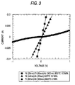
- Fig. 3 shows the current-voltage (I-V) characteristics of the respective samples (Ti/Al, Ni/Al, Ni/Ti/Al) after the heat treatment at 800 °C for 10 minutes.
- Fig. 4 shows the relationship between the film thickness of a Ni layer and Ti layer and the contact resistivity ( ⁇ c) in a sample having a laminated structure of Ni/Ti/Al.
- Fig. 5 is a schematic view of the structure of an SiC device 1 according to an embodiment of this invention.
- the SiC device can be manufactured by the following process.
- an n-type SiC substrate 10 is placed in a vapor-phase growing apparatus chamber.
- monosilane (SiH 4 ) and propane (C 3 H 8 ) which are a raw gas
- trimethylaluminum ((CH 3 )Al) which is an impurity gas
- the p-type SiC layer 11 can be also formed by known molecular beam epitaxy (MBE), halide vapor phase epitaxy (HVPE), sputtering, ion-plating, electron shower, etc.
- the substrate 10 is subjected to sacrificial oxidation in an atmosphere of O 2 for 60 minutes at 1150 °C to deposit an SiO 2 film 12 having about 10 nm on the surface of the p-type SiC layer 11.
- electrode patterning by photolithography is performed, a part of the SiO 2 film is removed using diluted hydrofluoric acid.
- an Ni layer 21 having a thickness of about 25 ⁇ m is formed by the electron beam method.
- a Ti layer 22 is formed by the electron beam method and an Al layer 23 is formed by the resistive heating.
- an electrode pattern is formed by a lift-off step.
- a p-type electrode 20 composed of Ni, Ti and Al which have been stacked in order is manufactured as shown in Fig. 5.
- an n-type electrode 30 which is composed of vanadium (V) and aluminum (Al) is formed on the surface of the n-type SiC substrate 10 by vapor deposition.
- the step of separating the chip is carried out using a scriber to provide the SiC device 1.
- This invention should not be limited to the embodiment described above. This invention includes various embodiments within a range which does not deviate from the scope of claim and can be easily anticipated by those skilled in the art. Further, it is needless to say that this invention can be applied to other semiconductor devices using SiC, e.g. III-group nitride compound semiconductor on SiC.
Landscapes
- Electrodes Of Semiconductors (AREA)
- Physical Vapour Deposition (AREA)
Abstract
Description
As seen from Fig. 1, the NiAl contact material provides the contact resistivity ρc on the order of 10-4 Ωcm2 at the concentration (40 at% or lower) lower than that of a TiAl contact material, and provides ρc of 9 x 10⁻⁵Ωcm2 at the Al concentration of 80 at %. With an increase in the Al concentration, the contact resistivity decreases. Thus, it was confirmed that Al plays an important part in the reduction of the contact resistivity. Further, after the heat treatment at 1000 °C also, NiAl provided a flatter surface than in TiAl.
Claims (15)
- An electrode for p-type SiC which contains a first electrode material of at least one selected from the group consisting of nickel (Ni), cobalt (Co), palladium (Pd) and platinum (Pt).
- An electrode for p-type SiC according to claim 1, which further contains a second electrode material of aluminum (Al).
- An electrode for p-type SiC according to claim 2, which further contains a third electrode material of titanium (Ti).
- An electrode for p-type SiC according to claim 1, wherein said first electrode material is Ni or Co.
- An electrode for p-type SiC according to claim 1, wherein the layer of said first electrode material is formed in contact with a p-type SiC layer.
- An electrode for p-type SiC including a first layer of at least one selected from the group consisting of nickel (Ni), cobalt (Co), palladium (Pd) and platinum (Pt) and a second layer of aluminum (Al), which are formed in order from the side of p-type SiC.
- An electrode for p-type SiC according to claim 6, which further contains a third layer of Ti formed between said first layer and said second layer.
- An SiC device, wherein the electrode for p-type SiC described in any one of claims 1 to 7 is formed on a p-type SiC layer.
- A method for manufacturing an electrode for p-type SiC comprising steps of:washing a p-type SiC layer;forming a first layer of at least one selected from the group consisting of nickel (Ni) , cobalt (Co) , palladium (Pd) and platinum (Pt); andheat-treating these layers.
- A method for manufacturing an electrode for p-type SiC comprising steps of:washing a p-type SiC layer;forming a first layer of at least one selected from the group consisting of nickel (Ni) , cobalt (Co) , palladium (Pd) and platinum (Pt);forming a second layer of aluminum (Al); andperforming heat treatment.
- A method for manufacturing an electrode for p-type SiC according to claim 10, further comprising a step of forming a third layer of titanium.
- A method for manufacturing an electrode for p-type SiC according to claim 11, comprising steps of:washing a p-type SiC layer;forming a first layer of at least one selected from the group consisting of nickel (Ni) , cobalt (Co) , palladium (Pd) and platinum (Pt);forming a third layer of titanium (Ti);forming a second layer of aluminum (Al); andperforming heat treatment.
- A method for manufacturing an electrode for p-type SiC according to claim 9, wherein said heat treatment is carried out at a temperature of 400 °C to 1100 °C.
- A method for manufacturing an electrode for p-type SiC according to claim 10, wherein said heat treatment is carried out at a temperature of 400 °C to 1100 °C.
- A method for manufacturing an SiC device including the steps of manufacturing the electrode for p-type SiC described in any one of claims 9 to 14.
Applications Claiming Priority (3)
| Application Number | Priority Date | Filing Date | Title |
|---|---|---|---|
| JP2001270771 | 2001-09-06 | ||
| JP2001270771A JP4026339B2 (en) | 2001-09-06 | 2001-09-06 | SiC electrode and manufacturing method thereof |
| PCT/JP2002/008883 WO2003023837A1 (en) | 2001-09-06 | 2002-09-02 | ELECTRODE FOR p-TYPE SiC |
Publications (2)
| Publication Number | Publication Date |
|---|---|
| EP1424725A1 true EP1424725A1 (en) | 2004-06-02 |
| EP1424725A4 EP1424725A4 (en) | 2005-08-03 |
Family
ID=19096383
Family Applications (1)
| Application Number | Title | Priority Date | Filing Date |
|---|---|---|---|
| EP02760799A Withdrawn EP1424725A4 (en) | 2001-09-06 | 2002-09-02 | ELECTRODE FOR P-TYPE SILICON CARBIDE |
Country Status (7)
| Country | Link |
|---|---|
| US (1) | US6943376B2 (en) |
| EP (1) | EP1424725A4 (en) |
| JP (1) | JP4026339B2 (en) |
| KR (1) | KR100532277B1 (en) |
| CN (1) | CN1473355A (en) |
| TW (1) | TWI270126B (en) |
| WO (1) | WO2003023837A1 (en) |
Families Citing this family (39)
| Publication number | Priority date | Publication date | Assignee | Title |
|---|---|---|---|---|
| JP4036075B2 (en) * | 2002-10-29 | 2008-01-23 | 豊田合成株式会社 | Method for manufacturing electrode for p-type SiC |
| KR100479650B1 (en) * | 2003-04-10 | 2005-04-07 | 주식회사 다윈 | A wafer with alternation design form and the semiconductor package manufacturing method therefor |
| JP4935075B2 (en) * | 2006-01-05 | 2012-05-23 | 住友電気工業株式会社 | Nitride semiconductor device with integrated electrode |
| JP5061473B2 (en) * | 2006-02-24 | 2012-10-31 | 住友電気工業株式会社 | Nitride semiconductor devices |
| US8432012B2 (en) | 2006-08-01 | 2013-04-30 | Cree, Inc. | Semiconductor devices including schottky diodes having overlapping doped regions and methods of fabricating same |
| US7728402B2 (en) * | 2006-08-01 | 2010-06-01 | Cree, Inc. | Semiconductor devices including schottky diodes with controlled breakdown |
| EP2631951B1 (en) * | 2006-08-17 | 2017-10-11 | Cree, Inc. | High power insulated gate bipolar transistors |
| JP4140648B2 (en) * | 2006-11-02 | 2008-08-27 | 住友電気工業株式会社 | Ohmic electrode for SiC semiconductor, method for producing ohmic electrode for SiC semiconductor, semiconductor device, and method for producing semiconductor device |
| JP5352954B2 (en) * | 2006-11-22 | 2013-11-27 | 日産自動車株式会社 | Electrode film / silicon carbide structure |
| JP5014749B2 (en) * | 2006-11-27 | 2012-08-29 | 三菱電機株式会社 | Method for manufacturing silicon carbide semiconductor device |
| US8835987B2 (en) | 2007-02-27 | 2014-09-16 | Cree, Inc. | Insulated gate bipolar transistors including current suppressing layers |
| JP5052169B2 (en) * | 2007-03-15 | 2012-10-17 | 新電元工業株式会社 | Method for manufacturing silicon carbide semiconductor device |
| US8866150B2 (en) * | 2007-05-31 | 2014-10-21 | Cree, Inc. | Silicon carbide power devices including P-type epitaxial layers and direct ohmic contacts |
| DE102007029829A1 (en) * | 2007-06-28 | 2009-01-02 | Infineon Technologies Austria Ag | Semiconductor component, has electrical contact structure with two metallic layers, where one of metallic layers is provided on other metallic layer such that latter metallic layer is surrounded by former metallic layer |
| JP5282382B2 (en) * | 2007-08-17 | 2013-09-04 | 富士電機株式会社 | Silicon carbide semiconductor device, manufacturing method thereof, and silicon carbide device |
| US8232558B2 (en) | 2008-05-21 | 2012-07-31 | Cree, Inc. | Junction barrier Schottky diodes with current surge capability |
| JP5408929B2 (en) * | 2008-08-21 | 2014-02-05 | 昭和電工株式会社 | Semiconductor device and manufacturing method of semiconductor device |
| WO2010047222A1 (en) * | 2008-10-23 | 2010-04-29 | 本田技研工業株式会社 | Electrode, semiconductor device, and method for manufacturing the semiconductor device |
| US8294507B2 (en) | 2009-05-08 | 2012-10-23 | Cree, Inc. | Wide bandgap bipolar turn-off thyristor having non-negative temperature coefficient and related control circuits |
| US8193848B2 (en) | 2009-06-02 | 2012-06-05 | Cree, Inc. | Power switching devices having controllable surge current capabilities |
| US8629509B2 (en) * | 2009-06-02 | 2014-01-14 | Cree, Inc. | High voltage insulated gate bipolar transistors with minority carrier diverter |
| US8541787B2 (en) * | 2009-07-15 | 2013-09-24 | Cree, Inc. | High breakdown voltage wide band-gap MOS-gated bipolar junction transistors with avalanche capability |
| US8354690B2 (en) | 2009-08-31 | 2013-01-15 | Cree, Inc. | Solid-state pinch off thyristor circuits |
| JP5401356B2 (en) * | 2010-02-09 | 2014-01-29 | 昭和電工株式会社 | Manufacturing method of semiconductor device |
| US9117739B2 (en) | 2010-03-08 | 2015-08-25 | Cree, Inc. | Semiconductor devices with heterojunction barrier regions and methods of fabricating same |
| US8415671B2 (en) | 2010-04-16 | 2013-04-09 | Cree, Inc. | Wide band-gap MOSFETs having a heterojunction under gate trenches thereof and related methods of forming such devices |
| US9142662B2 (en) | 2011-05-06 | 2015-09-22 | Cree, Inc. | Field effect transistor devices with low source resistance |
| US9029945B2 (en) | 2011-05-06 | 2015-05-12 | Cree, Inc. | Field effect transistor devices with low source resistance |
| WO2013036370A1 (en) | 2011-09-11 | 2013-03-14 | Cree, Inc. | High current density power module comprising transistors with improved layout |
| US8680587B2 (en) | 2011-09-11 | 2014-03-25 | Cree, Inc. | Schottky diode |
| US9640617B2 (en) | 2011-09-11 | 2017-05-02 | Cree, Inc. | High performance power module |
| US9373617B2 (en) | 2011-09-11 | 2016-06-21 | Cree, Inc. | High current, low switching loss SiC power module |
| US8664665B2 (en) | 2011-09-11 | 2014-03-04 | Cree, Inc. | Schottky diode employing recesses for elements of junction barrier array |
| US8618582B2 (en) | 2011-09-11 | 2013-12-31 | Cree, Inc. | Edge termination structure employing recesses for edge termination elements |
| WO2014074555A1 (en) * | 2012-11-06 | 2014-05-15 | CoLabs International Corporation | Composition containing a cellulose derived capsule with a sunscreen |
| WO2018062689A1 (en) | 2016-09-29 | 2018-04-05 | 주식회사 엘지화학 | Silicon-based melt composition and method for manufacturing silicon carbide single crystal using same |
| CN109786447B (en) * | 2017-11-13 | 2022-06-21 | 比亚迪半导体股份有限公司 | P-type SiC ohmic contact material and preparation method thereof |
| US12024794B2 (en) * | 2021-06-17 | 2024-07-02 | Wolfspeed, Inc. | Reduced optical absorption for silicon carbide crystalline materials |
| FR3126544B1 (en) * | 2021-08-31 | 2024-08-09 | Commissariat Energie Atomique | Resistive memory device and method of production |
Family Cites Families (8)
| Publication number | Priority date | Publication date | Assignee | Title |
|---|---|---|---|---|
| JPS63283014A (en) | 1987-04-28 | 1988-11-18 | Sharp Corp | Silicon carbide semiconductor element |
| JP2911122B2 (en) | 1988-04-20 | 1999-06-23 | 三洋電機株式会社 | Method for forming ohmic electrode of silicon carbide semiconductor device |
| JP2940699B2 (en) | 1990-07-30 | 1999-08-25 | 三洋電機株式会社 | Method for forming p-type SiC electrode |
| JPH0513812A (en) | 1991-07-04 | 1993-01-22 | Sharp Corp | Light emitting diode |
| US5323022A (en) | 1992-09-10 | 1994-06-21 | North Carolina State University | Platinum ohmic contact to p-type silicon carbide |
| US5338944A (en) | 1993-09-22 | 1994-08-16 | Cree Research, Inc. | Blue light-emitting diode with degenerate junction structure |
| US5739554A (en) | 1995-05-08 | 1998-04-14 | Cree Research, Inc. | Double heterojunction light emitting diode with gallium nitride active layer |
| DE19924982A1 (en) | 1998-06-08 | 1999-12-09 | Siemens Ag | Semiconductor structure, e.g. a Schottky diode, p-n diode or MOSFET, has a low contact resistance, temperature stable ohmic contact |
-
2001
- 2001-09-06 JP JP2001270771A patent/JP4026339B2/en not_active Expired - Fee Related
-
2002
- 2002-09-02 US US10/415,914 patent/US6943376B2/en not_active Expired - Fee Related
- 2002-09-02 KR KR10-2003-7006055A patent/KR100532277B1/en not_active Expired - Fee Related
- 2002-09-02 WO PCT/JP2002/008883 patent/WO2003023837A1/en not_active Ceased
- 2002-09-02 CN CNA028028295A patent/CN1473355A/en active Pending
- 2002-09-02 EP EP02760799A patent/EP1424725A4/en not_active Withdrawn
- 2002-09-05 TW TW091120274A patent/TWI270126B/en not_active IP Right Cessation
Also Published As
| Publication number | Publication date |
|---|---|
| TWI270126B (en) | 2007-01-01 |
| US6943376B2 (en) | 2005-09-13 |
| KR20040015018A (en) | 2004-02-18 |
| EP1424725A4 (en) | 2005-08-03 |
| US20040016929A1 (en) | 2004-01-29 |
| KR100532277B1 (en) | 2005-11-29 |
| CN1473355A (en) | 2004-02-04 |
| WO2003023837A1 (en) | 2003-03-20 |
| JP4026339B2 (en) | 2007-12-26 |
| JP2003077860A (en) | 2003-03-14 |
Similar Documents
| Publication | Publication Date | Title |
|---|---|---|
| US6943376B2 (en) | Electrode for p-type SiC | |
| US5597744A (en) | Method of producing a silicon carbide semiconductor device | |
| KR100827556B1 (en) | Method of growing a polycrystalline silicon layer, method of growing a single crystal silicon layer and catalytic CVD apparatus | |
| JP3705016B2 (en) | Translucent electrode film and group III nitride compound semiconductor device | |
| US7507650B2 (en) | Process for producing Schottky junction type semiconductor device | |
| EP0421397A1 (en) | Diamond semiconductor device and method of manufacture | |
| US7141498B2 (en) | Method of forming an ohmic contact in wide band semiconductor | |
| JP4100652B2 (en) | SiC Schottky diode | |
| JP3557791B2 (en) | Group III nitride semiconductor electrode and device having the electrode | |
| JPH01196873A (en) | Silicon carbide semiconductor device | |
| Shiau et al. | Localized epitaxial growth of CrSi2 on silicon | |
| US20240055257A1 (en) | Method for manufacturing a contact on a silicon carbide substrate, and silicon carbide semiconductor device | |
| TWI890939B (en) | Nucleation layers for growth of gallium-and-nitrogen-containing regions | |
| KR100537398B1 (en) | Method of forming ohmic electrode | |
| EP0697738B1 (en) | Semiconductor diamond device having improved metal-diamond contact | |
| CN114335169A (en) | Gallium nitride Schottky barrier diode and manufacturing method thereof | |
| WO1993002471A1 (en) | High temperature refractory silicide rectifying contact and method for making same | |
| CN114335195A (en) | Gallium nitride Schottky barrier diode with sub-vertical structure and manufacturing method thereof | |
| US9035323B2 (en) | Silicon carbide barrier diode | |
| JPH04233277A (en) | Transistor provided with layer of cubic boron nitride | |
| US7564062B2 (en) | Electrode for p-type SiC | |
| US5571391A (en) | Electrode structure and method for fabricating the same | |
| JP3439597B2 (en) | Ohmic electrode for n-type SiC and manufacturing method thereof | |
| WO2003069681A1 (en) | High performance active and passive structures based on silicon material grown epitaxially or bonded to silicon carbide substrate | |
| JP4742399B2 (en) | Method for producing group 3-5 compound semiconductor |
Legal Events
| Date | Code | Title | Description |
|---|---|---|---|
| PUAI | Public reference made under article 153(3) epc to a published international application that has entered the european phase |
Free format text: ORIGINAL CODE: 0009012 |
|
| 17P | Request for examination filed |
Effective date: 20030430 |
|
| AK | Designated contracting states |
Kind code of ref document: A1 Designated state(s): AT BE BG CH CY CZ DE DK EE ES FI FR GB GR IE IT LI LU MC NL PT SE SK TR |
|
| AX | Request for extension of the european patent |
Extension state: AL LT LV MK RO SI |
|
| RIN1 | Information on inventor provided before grant (corrected) |
Inventor name: SHIBATA, NAOKI,TOYODA GOSEI CO., LTD. Inventor name: MURAKAMI, MASANORI Inventor name: KOIDE, YASUO Inventor name: YASUKOCHI, RYUICHI Inventor name: KONISHI, RYOHEI Inventor name: NAKATSUKA, OSAMU,ROOM 2B,NISHIHATA-MANSION |
|
| A4 | Supplementary search report drawn up and despatched |
Effective date: 20050616 |
|
| RIC1 | Information provided on ipc code assigned before grant |
Ipc: 7H 01L 29/80 B Ipc: 7H 01L 21/28 B Ipc: 7H 01L 33/00 B Ipc: 7H 01L 29/45 B Ipc: 7H 01L 21/04 A |
|
| 17Q | First examination report despatched |
Effective date: 20050804 |
|
| STAA | Information on the status of an ep patent application or granted ep patent |
Free format text: STATUS: THE APPLICATION IS DEEMED TO BE WITHDRAWN |
|
| 18D | Application deemed to be withdrawn |
Effective date: 20100331 |