EP1422751A2 - Verfahren zum Plasmaätzen von Materialien mit hoher Dielektrizitätskonstante mit hoher Selektivität zu darunterangeordneten Schichten - Google Patents
Verfahren zum Plasmaätzen von Materialien mit hoher Dielektrizitätskonstante mit hoher Selektivität zu darunterangeordneten Schichten Download PDFInfo
- Publication number
- EP1422751A2 EP1422751A2 EP03257189A EP03257189A EP1422751A2 EP 1422751 A2 EP1422751 A2 EP 1422751A2 EP 03257189 A EP03257189 A EP 03257189A EP 03257189 A EP03257189 A EP 03257189A EP 1422751 A2 EP1422751 A2 EP 1422751A2
- Authority
- EP
- European Patent Office
- Prior art keywords
- gas
- maintaining
- computer
- hafnium
- dielectric material
- Prior art date
- Legal status (The legal status is an assumption and is not a legal conclusion. Google has not performed a legal analysis and makes no representation as to the accuracy of the status listed.)
- Withdrawn
Links
Images


Classifications
-
- H—ELECTRICITY
- H10—SEMICONDUCTOR DEVICES; ELECTRIC SOLID-STATE DEVICES NOT OTHERWISE PROVIDED FOR
- H10P—GENERIC PROCESSES OR APPARATUS FOR THE MANUFACTURE OR TREATMENT OF DEVICES COVERED BY CLASS H10
- H10P50/00—Etching of wafers, substrates or parts of devices
- H10P50/20—Dry etching; Plasma etching; Reactive-ion etching
- H10P50/28—Dry etching; Plasma etching; Reactive-ion etching of insulating materials
- H10P50/282—Dry etching; Plasma etching; Reactive-ion etching of insulating materials of inorganic materials
- H10P50/283—Dry etching; Plasma etching; Reactive-ion etching of insulating materials of inorganic materials by chemical means
- H10P50/285—Dry etching; Plasma etching; Reactive-ion etching of insulating materials of inorganic materials by chemical means of materials not containing Si, e.g. PZT or Al2O3
Definitions
- the present invention relates generally to a method of dry etching semiconductor wafers. More specifically, the invention relates to a method of etching high-K dielectric materials using a gas mixture comprising a halogen gas and a hydrocarbon gas.
- Field effect transistors that are used in forming integrated circuit generally utilize a polysilicon gate electrode deposited upon a gate dielectric that separates the electrode from the channel between the source and the drain regions.
- the gate dielectric is typically fabricated of silicon dioxide (SiO 2 ).
- SiO 2 silicon dioxide
- the thickness of the dielectric material in the gate structure has become thinner than 10 Angstroms. With such a thin dielectric, electrons can propagate from the polysilicon gate electrode into the transistor channel causing the transistor to operate improperly or become defective.
- hafnium-dioxide HfO 2
- hafnium-silicate HfSiO 2
- hafnium-dioxide and hafnium-silicate are such stable dielectric materials that it is very difficult to etch either of them by using conventional oxide etchants to form gate structures without damaging other layers of material residing on the wafer.
- high-K dielectrics such as hafnium-dioxide and hafnium-silicate have found limited use in semiconductor devices.
- etching materials with high dielectric constants such as HfO 2 , HFSiO 2 , ZrO 2 , Al 2 O 3 , BST, PZK, ZrSiO 2 , TaO 2 , and the like using a gas mixture comprising a halogen gas and hydrocarbon gas.
- a gas mixture comprising a halogen gas and hydrocarbon gas.
- an etch gas or mixture
- chlorine Cl 2
- CH 4 methane
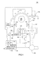
- FIG. 1 depicts a schematic diagram of a plasma processing apparatus of the kind used in performing the etching processes according to one embodiment of the present invention
- FIG. 2 depicts a flow diagram of method for performing an etching process for a high-K dielectric material
- FIG. 3A depicts a schematic cross-sectional view of a wafer having a high-K dielectric layer undergoing an etching process in accordance with the method of FIG. 2;
- FIG. 3B depicts a schematic cross-sectional view of a gate structure formed during the etching process in accordance with the method of FIG. 2;
- FIG. 4 is a table summarizing the processing parameters of one embodiment of the inventive method when practiced using the apparatus of FIG. 1.
- the present invention is a method of etching materials with high dielectric constants (high-K materials have dielectric constants greater than 4.0) using a plasma generated from a gas (or gas mixture) comprising gases containing a halogen gas, such as Cl 2 , HCl and the like, as well as a hydrocarbon gas, such as methane (CH 4 ), ethylene (C 2 H 4 ), propane (C 3 H 8 ), butane (C 4 H 10 ), and the like.
- a reducing gas such as carbon monoxide (CO)
- the high-K materials include HfO 2 , ZrO 2 , Al 2 O 3 , BST, PZK, ZrSiO 2 , HfSiO 2 , TaO 2 , and the like.
- the type of halogen gas (e.g., Cl 2 ) is selected to best remove the metal from the dielectric layer.
- the hydrocarbon e.g., methane
- the methane is selected to best serve as a polymerizing gas to combine with by-products produced during the etch process.
- the methane is used to suppress the silicon etch rate, such that a high high-K dielectric (e.g., HfO 2 or HfSiO 2 ) to silicon selectivity is obtained.
- the type of reducing gas is selected to best remove the oxygen from the dielectric layer.
- the etch process of the present invention can be reduced to practice in any plasma etch chamber, for example, a Decoupled Plasma Source (DPS) etch process chamber or a DPS-II etch process chamber, both of which are available from Applied Materials, Inc. of Santa Clara, California.
- DPS Decoupled Plasma Source
- DPS-II DPS-II etch process chamber
- FIG. 1 depicts a schematic diagram of the DPS etch process chamber 100, that comprises at least one inductive coil antenna segment 112, positioned exterior to a dielectric, dome-shaped ceiling 120 (referred to herein as the dome 120).
- Other chambers may have other types of ceilings, e.g., a flat ceiling.
- the antenna segment 112 is coupled to an upper radio-frequency (RF) source 118 through a matching network 119.
- RF radio-frequency
- the RF power applied to the inductive coil antenna 112 is in a range between about 200 to 2500 Watts at a frequency between about 50 kHz and 13.56 MHz.
- the process chamber 100 also includes a substrate support pedestal (biasing element, e.g., cathode) 116 that is coupled to a second (biasing) RF source 122 that is generally capable of producing an RF signal having bias power between about 5 and 500 Watts at a frequency of approximately 13.56 MHz.
- the biasing source 122 is coupled to the biasing element 116 through a matching network 123.
- the chamber 100 also contains a conductive chamber wall 130 that is connected to an electrical ground 134.
- a controller 140 comprising a central processing unit (CPU) 144, a memory 142, and support circuits 146 for the CPU 144 is coupled to the various components of the DPS etch process chamber 100 to facilitate control of the etch process.
- CPU central processing unit
- a semiconductor substrate 114 is placed on the substrate support pedestal 116 and is retained thereon by conventional techniques, such as electrostatic chucking or mechanical clamping of the substrate 114.
- Gaseous components are supplied from a gas panel 138 to the process chamber 100 through entry ports 126 to form a gaseous mixture 150.
- the gaseous mixture 150 is ignited into a plasma 152 in the process chamber 100 by applying RF power from the RF sources 118 and 122 respectively to the antenna 112 and the biasing element (e.g., chucking electrode) 116.
- the pressure within the interior of the etch chamber 100 is controlled using a throttle valve 127 situated between the chamber 100 and a vacuum pump 136.
- the temperature at the surface of the chamber walls 130 is controlled using liquid-containing conduits (not shown) that are located in the walls 130 of the chamber 100.
- the temperature of the substrate 114 is controlled by stabilizing the temperature of the support pedestal 116 and flowing helium gas from source 148 via conduit 149 to channels formed by the back of the substrate 114 and grooves (not shown) on the pedestal surface.
- the helium gas is used to facilitate heat transfer between the pedestal 116 and the substrate 114.
- the substrate 114 is heated by a resistive heater 125 within the pedestal 116 to a steady state temperature via a DC power source 125, and the helium facilitates uniform heating of the substrate 114.
- the substrate 114 is maintained at a temperature of between 10 and 500 degrees Celsius.
- etch chambers may be used to practice the invention.
- chambers with remote plasma sources microwave plasma chambers, electron cyclotron resonance (ECR) plasma chambers, and the like may be utilized as well to practice the invention.
- ECR electron cyclotron resonance
- the CPU 144 may be one of any form of general-purpose computer processor that can be used in an industrial setting for controlling various chambers and subprocessors.
- the memory 142 is coupled to the CPU 144.
- the memory 142, or computer-readable medium may be one or more of readily available memory such as random access memory (RAM), read only memory (ROM), floppy disk, hard disk, or any other form of digital storage, local or remote.
- the support circuits 146 are coupled to the CPU 144 for supporting the processor in a conventional manner. These circuits include cache, power supplies, clock circuits, input/output circuitry and subsystems, and the like.
- An etching process 200 is generally stored in the memory 142 as a software routine 202.
- the software routine 202 may also be stored and/or executed by a second CPU (not shown) that is remotely located from the hardware being controlled by the CPU 144.
- the specific embodiment of the etching process 200 depicted in Fig. 2 comprises the steps of applying bias power to the pedestal (step 204); supplying a halogen gas such as chlorine (Cl 2 ) to the chamber 100 (step 206); supplying a hydrocarbon such as methane (CH 4 ) to the chamber 100 (step 208); and regulating the pressure of the Cl 2 and CH 4 (step 210).
- RF power is applied to form a plasma (step 212), and the wafer temperature is regulated (step 214).
- the silicon is etched (step 216) for a duration that continues until an unmasked portion of high-K dielectric (e.g., hafnium-dioxide, hafnium-silicate, and the like) is removed.
- the etch time is terminated upon a certain optical emission occurring, upon a particular duration occurring or upon some other indicator determining that the hafnium-dioxide has been removed.
- steps of the process 200 need not be performed sequentially. For example, some or all of the steps may be performed simultaneously or in another order to etch a hafnium-dioxide, hafnium-silicate, or other high-K dielectric layer.
- the software routine 202 is discussed with respect to FIG. 1 and FIG. 2.
- the software routine 202 is executed after a wafer 114 is positioned on the pedestal 116.
- the software routine 202 when executed by the CPU 144, transforms the general-purpose computer into a specific purpose computer (controller) 140 that controls the chamber operation such that the etching process 200 is performed.
- controller controller
- the process of the present invention is discussed as being implemented as a software routine, some of the method steps that are disclosed therein may be performed in hardware as well as by the software controller.
- the invention may be implemented in software as executed upon a computer system, in hardware as an application specific integrated circuit or other type of hardware implementation, or a combination of software and hardware.
- a wafer or other form of workpiece 114 is etched, for example, by applying a bias power in the range of 0-100 Watts to the pedestal 116 in step 204.
- the gaseous mixture 150 is supplied to the chamber 100 at a rate in the range of 5-300 sccm Cl 2 and 2-200 sccm CH 4 in steps 206 and 208, respectively.
- Such flow rates define a flow ratio of Cl 2 to CH 4 in the range of (0.025:1) to (150:1). In one specific embodiment, the flow ratio of Cl 2 to CH 4 is about 4:1.
- the total pressure of the gas mixture 150 is regulated to maintain a pressure in the range of 2-100 mTorr.
- a reducing gas such as carbon monoxide (CO) is added to the mixture 150.
- CO carbon monoxide
- adding carbon monoxide to the mixture 150 helps reduce oxygen from the dielectric layer that may be present.
- the gaseous mixture 150 supplied to the chamber 100 comprises Cl 2 at a rate in a range of about 5-300 sccm, CH 4 in a range of about 2-200 sccm, and CO in a range of about 5-300 sccm.
- the flow rates define a flow ratio of Cl 2 to CH 4 in a range of about (0.025:1) to (150:1), a flow ratio of Cl 2 to CO in a range of about (0.016:1) to (150:1), and a flow ratio of CO to CH 4 in a range of about (0.025:1) to (150:1).
- the flow ratio of Cl 2 to CH 4 to CO is 1:1:0.5.
- step 212 applies 200-2500 Watts of RF power to the antenna 112, and plasma 152 is formed.
- the wafer 114 is heated to 10-500 degrees Celsius in step 214. Etching of the wafer 114 occurs in step 216.
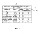
- the processing chamber 100 has a pedestal bias power of 20 watts, a gas flow rate of 40 sccm of Cl 2 and 10 sccm of CH 4 , a chamber pressure of 4 mTorr, an antenna power of 1100 watts, and a pedestal temperature of 350° C.
- the chamber 100 uses a pedestal bias power of 50 watts, a gas flow rate of 40 sccm of Cl 2 and 10 sccm of CH 4 , a chamber pressure of 4 mTorr, an antenna power of 400 watts, and a pedestal temperature of 250° C.
- FIG. 4 presents a table 400 summarizing the etch process parameters through which one can practice the invention using a DPS Centura® system.
- the etch process parameters for one embodiment of the invention presented above are summarized in column 402.
- the process ranges are presented in column 404. It should be understood, however, that the use of a different chamber may necessitate different process parameter values and ranges.
- FIG. 3A depicts a schematic cross-sectional view of a wafer 114 having a high-K dielectric layer 302 undergoing an etching process in accordance with the method 200 of FIG. 2.
- the wafer 114 comprises a doped layer 314 having a drain region 350, a source region 352 and a channel 354 therebetween, a silicon dioxide layer 304 (optional), a high-K dielectric layer 302, a polysilicon layer 306, and an etch mask 308.
- the mask 308 may be a photoresist mask or a hard mask (e.g., SiO 2 , SiN, amorphous carbon, and the like).
- the etch mask 308 is illustratively patterned to form a gate region 316 over the channel 354.
- FIG. 3A shows the remaining stack layers 310 of the structure after a previous etching step was performed to etch the polysilicon layer 306 and form the gate region 316 under the mask 308.
- the previous etch step to etch the polysilicon layer 306 is performed in a conventional manner.
- the mask 308 also leaves a portion 312 of the high-K dielectric layer 302 exposed to the etch chemistry for further processing in accordance with the method 200 discussed above with regard to FIG. 2.
- An underlying, optional silicon dioxide layer 304 is conventionally etched after the high-K dielectric in region 312 is removed.
- the high-K dielectric material 302 is hafnium-silicate (HfSiO 2 )
- the etching process is performed at temperatures greater than 100°C
- the hafnium-silicate is etched using the Cl 2 /CH 4 chemistry at a rate of about 100 ⁇ /min with a selectivity to SiO 2 of greater than 3:1.
- the selectivity to silicon and polysilicon is also greater than 3:1.
- the hafnium-dioxide is etched by the Cl 2 /CH 4 chemistry at a rate of about 100 ⁇ /min with a selectivity to SiO 2 of greater than 10:1.
- the selectivity to silicon and polysilicon is greater than 3:1.
- FIG. 3B depicts a schematic cross-sectional view of a gate structure comprising the high-K dielectric layer of FIG. 3A that has been etched using a chlorine and methane etching chemistry according to an example of the present invention.
- FIG. 3B depicts a schematic cross-sectional view of a gate structure 316 formed during the etching process in accordance with the method 200 of FIG. 2. Specifically, the profile shown in FIG. 3B illustrates the wafer 114 of FIG. 3A after completion of the etching process.
- the high-K dielectric layer ensures that, during transistor operation, electrons will not flow (leak) from the gate electrode to the channel. Typically, the thickness of the high-K dielectric is less than 5 nanometers.
- the invention may be practiced in other etching equipment wherein the processing parameters may be adjusted to achieve acceptable etch characteristics by those skilled in the arts by utilizing the teachings disclosed herein without departing from the spirit of the invention.
Landscapes
- Drying Of Semiconductors (AREA)
Applications Claiming Priority (2)
| Application Number | Priority Date | Filing Date | Title |
|---|---|---|---|
| US10/301,239 US7217665B2 (en) | 2002-11-20 | 2002-11-20 | Method of plasma etching high-K dielectric materials with high selectivity to underlying layers |
| US301239 | 2002-11-20 |
Publications (2)
| Publication Number | Publication Date |
|---|---|
| EP1422751A2 true EP1422751A2 (de) | 2004-05-26 |
| EP1422751A3 EP1422751A3 (de) | 2005-03-30 |
Family
ID=32229896
Family Applications (1)
| Application Number | Title | Priority Date | Filing Date |
|---|---|---|---|
| EP03257189A Withdrawn EP1422751A3 (de) | 2002-11-20 | 2003-11-14 | Verfahren zum Plasmaätzen von Materialien mit hoher Dielektrizitätskonstante mit hoher Selektivität zu darunterangeordneten Schichten |
Country Status (2)
| Country | Link |
|---|---|
| US (1) | US7217665B2 (de) |
| EP (1) | EP1422751A3 (de) |
Cited By (2)
| Publication number | Priority date | Publication date | Assignee | Title |
|---|---|---|---|---|
| WO2004109772A3 (en) * | 2003-05-30 | 2005-04-14 | Tokyo Electron Ltd | Method and system for etching a high-k dielectric material |
| WO2007030522A3 (en) * | 2005-09-09 | 2007-05-03 | Lam Res Corp | Selectivity etch of films with high dielectric constant with h2 addition |
Families Citing this family (9)
| Publication number | Priority date | Publication date | Assignee | Title |
|---|---|---|---|---|
| US7067439B2 (en) | 2002-06-14 | 2006-06-27 | Applied Materials, Inc. | ALD metal oxide deposition process using direct oxidation |
| JP2005039015A (ja) * | 2003-07-18 | 2005-02-10 | Hitachi High-Technologies Corp | プラズマ処理方法および装置 |
| US8119210B2 (en) | 2004-05-21 | 2012-02-21 | Applied Materials, Inc. | Formation of a silicon oxynitride layer on a high-k dielectric material |
| US7431795B2 (en) * | 2004-07-29 | 2008-10-07 | Applied Materials, Inc. | Cluster tool and method for process integration in manufacture of a gate structure of a field effect transistor |
| US7837838B2 (en) | 2006-03-09 | 2010-11-23 | Applied Materials, Inc. | Method of fabricating a high dielectric constant transistor gate using a low energy plasma apparatus |
| US7678710B2 (en) | 2006-03-09 | 2010-03-16 | Applied Materials, Inc. | Method and apparatus for fabricating a high dielectric constant transistor gate using a low energy plasma system |
| US7645710B2 (en) | 2006-03-09 | 2010-01-12 | Applied Materials, Inc. | Method and apparatus for fabricating a high dielectric constant transistor gate using a low energy plasma system |
| TWI435376B (zh) | 2006-09-26 | 2014-04-21 | 應用材料股份有限公司 | 用於缺陷鈍化之高k閘極堆疊的氟電漿處理 |
| US20090197421A1 (en) * | 2008-01-31 | 2009-08-06 | Micron Technology, Inc. | Chemistry and compositions for manufacturing integrated circuits |
Family Cites Families (27)
| Publication number | Priority date | Publication date | Assignee | Title |
|---|---|---|---|---|
| US110992A (en) * | 1871-01-17 | Ohaeles moeeill | ||
| JP3115715B2 (ja) | 1992-11-12 | 2000-12-11 | 三菱電機株式会社 | 高誘電率を有する多元系酸化物膜のエッチング方法、高融点金属含有膜のエッチング方法および薄膜キャパシタ素子の製造方法 |
| US5431778A (en) | 1994-02-03 | 1995-07-11 | Motorola, Inc. | Dry etch method using non-halocarbon source gases |
| US5776356A (en) * | 1994-07-27 | 1998-07-07 | Sharp Kabushiki Kaisha | Method for etching ferroelectric film |
| US5814563A (en) * | 1996-04-29 | 1998-09-29 | Applied Materials, Inc. | Method for etching dielectric using fluorohydrocarbon gas, NH3 -generating gas, and carbon-oxygen gas |
| US5972758A (en) * | 1997-12-04 | 1999-10-26 | Intel Corporation | Pedestal isolated junction structure and method of manufacture |
| US6432785B1 (en) * | 1998-02-19 | 2002-08-13 | Texas Instruments-Acer Incorporated | Method for fabricating ultra short channel PMOSFET with buried source/drain junctions and self-aligned silicide |
| JPH11293481A (ja) | 1998-04-14 | 1999-10-26 | Toshiba Corp | 薄膜処理方法及びその装置 |
| US6232174B1 (en) * | 1998-04-22 | 2001-05-15 | Sharp Kabushiki Kaisha | Methods for fabricating a semiconductor memory device including flattening of a capacitor dielectric film |
| US6235593B1 (en) * | 1999-02-18 | 2001-05-22 | Taiwan Semiconductor Manufacturing Company | Self aligned contact using spacers on the ILD layer sidewalls |
| US6228731B1 (en) * | 1999-08-16 | 2001-05-08 | Taiwan Semiconductor Manufacturing Company | Re-etched spacer process for a self-aligned structure |
| US6368518B1 (en) * | 1999-08-25 | 2002-04-09 | Micron Technology, Inc. | Methods for removing rhodium- and iridium-containing films |
| US6242331B1 (en) * | 1999-12-20 | 2001-06-05 | Taiwan Semiconductor Manufacturing Company | Method to reduce device contact resistance using a hydrogen peroxide treatment |
| US6485988B2 (en) * | 1999-12-22 | 2002-11-26 | Texas Instruments Incorporated | Hydrogen-free contact etch for ferroelectric capacitor formation |
| JP4686006B2 (ja) * | 2000-04-27 | 2011-05-18 | 大日本印刷株式会社 | ハーフトーン位相シフトフォトマスクとハーフトーン位相シフトフォトマスク用ブランクス、及びハーフトーン位相シフトフォトマスクの製造方法 |
| US6437377B1 (en) * | 2001-01-24 | 2002-08-20 | International Business Machines Corporation | Low dielectric constant sidewall spacer using notch gate process |
| US6620733B2 (en) | 2001-02-12 | 2003-09-16 | Lam Research Corporation | Use of hydrocarbon addition for the elimination of micromasking during etching of organic low-k dielectrics |
| US6451673B1 (en) * | 2001-02-15 | 2002-09-17 | Advanced Micro Devices, Inc. | Carrier gas modification for preservation of mask layer during plasma etching |
| US6509219B2 (en) * | 2001-03-19 | 2003-01-21 | International Business Machines Corporation | Fabrication of notched gates by passivating partially etched gate sidewalls and then using an isotropic etch |
| DE10114778A1 (de) * | 2001-03-26 | 2002-10-17 | Infineon Technologies Ag | Verfahren zur Herstellung eines MOSFETs mit sehr kleiner Kanallänge |
| KR100355035B1 (en) * | 2001-04-03 | 2002-10-05 | Samsung Electronics Co Ltd | Method for fabricating semiconductor device by using notch gate |
| JP2003059906A (ja) | 2001-07-31 | 2003-02-28 | Applied Materials Inc | エッチング方法およびキャパシタを形成する方法 |
| US6451647B1 (en) * | 2002-03-18 | 2002-09-17 | Advanced Micro Devices, Inc. | Integrated plasma etch of gate and gate dielectric and low power plasma post gate etch removal of high-K residual |
| US7094704B2 (en) * | 2002-05-09 | 2006-08-22 | Applied Materials, Inc. | Method of plasma etching of high-K dielectric materials |
| US20040014327A1 (en) * | 2002-07-18 | 2004-01-22 | Bing Ji | Method for etching high dielectric constant materials and for cleaning deposition chambers for high dielectric constant materials |
| US6727150B2 (en) * | 2002-07-26 | 2004-04-27 | Micron Technology, Inc. | Methods of forming trench isolation within a semiconductor substrate including, Tshaped trench with spacers |
| WO2004109772A2 (en) | 2003-05-30 | 2004-12-16 | Tokyo Electron Limited | Method and system for etching a high-k dielectric material |
-
2002
- 2002-11-20 US US10/301,239 patent/US7217665B2/en not_active Expired - Fee Related
-
2003
- 2003-11-14 EP EP03257189A patent/EP1422751A3/de not_active Withdrawn
Cited By (3)
| Publication number | Priority date | Publication date | Assignee | Title |
|---|---|---|---|---|
| WO2004109772A3 (en) * | 2003-05-30 | 2005-04-14 | Tokyo Electron Ltd | Method and system for etching a high-k dielectric material |
| US7709397B2 (en) | 2003-05-30 | 2010-05-04 | Tokyo Electron Limited | Method and system for etching a high-k dielectric material |
| WO2007030522A3 (en) * | 2005-09-09 | 2007-05-03 | Lam Res Corp | Selectivity etch of films with high dielectric constant with h2 addition |
Also Published As
| Publication number | Publication date |
|---|---|
| US7217665B2 (en) | 2007-05-15 |
| US20040097092A1 (en) | 2004-05-20 |
| EP1422751A3 (de) | 2005-03-30 |
Similar Documents
| Publication | Publication Date | Title |
|---|---|---|
| US6806095B2 (en) | Method of plasma etching of high-K dielectric materials with high selectivity to underlying layers | |
| US7838434B2 (en) | Method of plasma etching of high-K dielectric materials | |
| US20060252265A1 (en) | Etching high-kappa dielectric materials with good high-kappa foot control and silicon recess control | |
| US6767824B2 (en) | Method of fabricating a gate structure of a field effect transistor using an alpha-carbon mask | |
| US6902681B2 (en) | Method for plasma etching of high-K dielectric materials | |
| US20040007561A1 (en) | Method for plasma etching of high-K dielectric materials | |
| US6277763B1 (en) | Plasma processing of tungsten using a gas mixture comprising a fluorinated gas and oxygen | |
| US8501626B2 (en) | Methods for high temperature etching a high-K material gate structure | |
| US6759286B2 (en) | Method of fabricating a gate structure of a field effect transistor using a hard mask | |
| CN1333308C (zh) | 控制蚀刻工序的精确度和再现性的方法 | |
| US9054048B2 (en) | NH3 containing plasma nitridation of a layer on a substrate | |
| US20070295455A1 (en) | Method and apparatus for etching material layers with high uniformity of a lateral etch rate across a substrate | |
| US8481433B2 (en) | Methods and apparatus for forming nitrogen-containing layers | |
| US6855643B2 (en) | Method for fabricating a gate structure | |
| KR20050028781A (ko) | 선택적 측벽 폴리머 증착에 의해 포토레지스트 트리밍공정의 임계크기 미세로딩을 제어하는 방법 | |
| TWI867885B (zh) | 用於圖案化應用的高密度碳膜 | |
| US7217665B2 (en) | Method of plasma etching high-K dielectric materials with high selectivity to underlying layers | |
| JP2022034956A (ja) | エッチング方法及びプラズマ処理装置 | |
| US20050176191A1 (en) | Method for fabricating a notched gate structure of a field effect transistor | |
| US20040132311A1 (en) | Method of etching high-K dielectric materials | |
| US7883631B2 (en) | Plasma etching method, plasma etching apparatus, control program and computer-readable storage medium | |
| TWI895415B (zh) | 用於光阻底層應用之矽碳化物膜的乾式蝕刻方法 | |
| US20050098536A1 (en) | Method of etching oxide with high selectivity |
Legal Events
| Date | Code | Title | Description |
|---|---|---|---|
| PUAI | Public reference made under article 153(3) epc to a published international application that has entered the european phase |
Free format text: ORIGINAL CODE: 0009012 |
|
| AK | Designated contracting states |
Kind code of ref document: A2 Designated state(s): AT BE BG CH CY CZ DE DK EE ES FI FR GB GR HU IE IT LI LU MC NL PT RO SE SI SK TR |
|
| AX | Request for extension of the european patent |
Extension state: AL LT LV MK |
|
| PUAL | Search report despatched |
Free format text: ORIGINAL CODE: 0009013 |
|
| AK | Designated contracting states |
Kind code of ref document: A3 Designated state(s): AT BE BG CH CY CZ DE DK EE ES FI FR GB GR HU IE IT LI LU MC NL PT RO SE SI SK TR |
|
| AX | Request for extension of the european patent |
Extension state: AL LT LV MK |
|
| 17P | Request for examination filed |
Effective date: 20050513 |
|
| AKX | Designation fees paid |
Designated state(s): DE FR GB IT NL |
|
| 17Q | First examination report despatched |
Effective date: 20050921 |
|
| STAA | Information on the status of an ep patent application or granted ep patent |
Free format text: STATUS: THE APPLICATION IS DEEMED TO BE WITHDRAWN |
|
| 18D | Application deemed to be withdrawn |
Effective date: 20100601 |