EP1420437A1 - METHOD OF PRODUCING SEMICONDUCTOR THIN FILM, METHOD OF PRODUCING SEMICONDUCTOR DEVICE, SEMICONDUCTOR DEVICE, INTEGRATED CIRCUIT, ELECTROOPTICAL DEVICE AND ELECTRONIC APPARATUS - Google Patents
METHOD OF PRODUCING SEMICONDUCTOR THIN FILM, METHOD OF PRODUCING SEMICONDUCTOR DEVICE, SEMICONDUCTOR DEVICE, INTEGRATED CIRCUIT, ELECTROOPTICAL DEVICE AND ELECTRONIC APPARATUS Download PDFInfo
- Publication number
- EP1420437A1 EP1420437A1 EP02749337A EP02749337A EP1420437A1 EP 1420437 A1 EP1420437 A1 EP 1420437A1 EP 02749337 A EP02749337 A EP 02749337A EP 02749337 A EP02749337 A EP 02749337A EP 1420437 A1 EP1420437 A1 EP 1420437A1
- Authority
- EP
- European Patent Office
- Prior art keywords
- film
- hole
- insulating film
- silicon film
- amorphous silicon
- Prior art date
- Legal status (The legal status is an assumption and is not a legal conclusion. Google has not performed a legal analysis and makes no representation as to the accuracy of the status listed.)
- Withdrawn
Links
Images







Classifications
-
- H—ELECTRICITY
- H10—SEMICONDUCTOR DEVICES; ELECTRIC SOLID-STATE DEVICES NOT OTHERWISE PROVIDED FOR
- H10D—INORGANIC ELECTRIC SEMICONDUCTOR DEVICES
- H10D30/00—Field-effect transistors [FET]
- H10D30/60—Insulated-gate field-effect transistors [IGFET]
- H10D30/67—Thin-film transistors [TFT]
-
- H—ELECTRICITY
- H10—SEMICONDUCTOR DEVICES; ELECTRIC SOLID-STATE DEVICES NOT OTHERWISE PROVIDED FOR
- H10P—GENERIC PROCESSES OR APPARATUS FOR THE MANUFACTURE OR TREATMENT OF DEVICES COVERED BY CLASS H10
- H10P14/00—Formation of materials, e.g. in the shape of layers or pillars
- H10P14/20—Formation of materials, e.g. in the shape of layers or pillars of semiconductor materials
- H10P14/38—Formation of materials, e.g. in the shape of layers or pillars of semiconductor materials characterised by treatments done after the formation of the materials
- H10P14/3802—Crystallisation or recrystallisation of non-monocrystalline semiconductor materials, e.g. regrowth
- H10P14/3808—Crystallisation or recrystallisation of non-monocrystalline semiconductor materials, e.g. regrowth using laser beams
- H10P14/3816—Pulsed laser beam
-
- C—CHEMISTRY; METALLURGY
- C23—COATING METALLIC MATERIAL; COATING MATERIAL WITH METALLIC MATERIAL; CHEMICAL SURFACE TREATMENT; DIFFUSION TREATMENT OF METALLIC MATERIAL; COATING BY VACUUM EVAPORATION, BY SPUTTERING, BY ION IMPLANTATION OR BY CHEMICAL VAPOUR DEPOSITION, IN GENERAL; INHIBITING CORROSION OF METALLIC MATERIAL OR INCRUSTATION IN GENERAL
- C23C—COATING METALLIC MATERIAL; COATING MATERIAL WITH METALLIC MATERIAL; SURFACE TREATMENT OF METALLIC MATERIAL BY DIFFUSION INTO THE SURFACE, BY CHEMICAL CONVERSION OR SUBSTITUTION; COATING BY VACUUM EVAPORATION, BY SPUTTERING, BY ION IMPLANTATION OR BY CHEMICAL VAPOUR DEPOSITION, IN GENERAL
- C23C16/00—Chemical coating by decomposition of gaseous compounds, without leaving reaction products of surface material in the coating, i.e. chemical vapour deposition [CVD] processes
- C23C16/44—Chemical coating by decomposition of gaseous compounds, without leaving reaction products of surface material in the coating, i.e. chemical vapour deposition [CVD] processes characterised by the method of coating
- C23C16/4401—Means for minimising impurities, e.g. dust, moisture or residual gas, in the reaction chamber
-
- C—CHEMISTRY; METALLURGY
- C23—COATING METALLIC MATERIAL; COATING MATERIAL WITH METALLIC MATERIAL; CHEMICAL SURFACE TREATMENT; DIFFUSION TREATMENT OF METALLIC MATERIAL; COATING BY VACUUM EVAPORATION, BY SPUTTERING, BY ION IMPLANTATION OR BY CHEMICAL VAPOUR DEPOSITION, IN GENERAL; INHIBITING CORROSION OF METALLIC MATERIAL OR INCRUSTATION IN GENERAL
- C23C—COATING METALLIC MATERIAL; COATING MATERIAL WITH METALLIC MATERIAL; SURFACE TREATMENT OF METALLIC MATERIAL BY DIFFUSION INTO THE SURFACE, BY CHEMICAL CONVERSION OR SUBSTITUTION; COATING BY VACUUM EVAPORATION, BY SPUTTERING, BY ION IMPLANTATION OR BY CHEMICAL VAPOUR DEPOSITION, IN GENERAL
- C23C16/00—Chemical coating by decomposition of gaseous compounds, without leaving reaction products of surface material in the coating, i.e. chemical vapour deposition [CVD] processes
- C23C16/44—Chemical coating by decomposition of gaseous compounds, without leaving reaction products of surface material in the coating, i.e. chemical vapour deposition [CVD] processes characterised by the method of coating
- C23C16/4411—Cooling of the reaction chamber walls
-
- C—CHEMISTRY; METALLURGY
- C30—CRYSTAL GROWTH
- C30B—SINGLE-CRYSTAL GROWTH; UNIDIRECTIONAL SOLIDIFICATION OF EUTECTIC MATERIAL OR UNIDIRECTIONAL DEMIXING OF EUTECTOID MATERIAL; REFINING BY ZONE-MELTING OF MATERIAL; PRODUCTION OF A HOMOGENEOUS POLYCRYSTALLINE MATERIAL WITH DEFINED STRUCTURE; SINGLE CRYSTALS OR HOMOGENEOUS POLYCRYSTALLINE MATERIAL WITH DEFINED STRUCTURE; AFTER-TREATMENT OF SINGLE CRYSTALS OR A HOMOGENEOUS POLYCRYSTALLINE MATERIAL WITH DEFINED STRUCTURE; APPARATUS THEREFOR
- C30B25/00—Single-crystal growth by chemical reaction of reactive gases, e.g. chemical vapour-deposition growth
- C30B25/02—Epitaxial-layer growth
- C30B25/08—Reaction chambers; Selection of materials therefor
-
- C—CHEMISTRY; METALLURGY
- C30—CRYSTAL GROWTH
- C30B—SINGLE-CRYSTAL GROWTH; UNIDIRECTIONAL SOLIDIFICATION OF EUTECTIC MATERIAL OR UNIDIRECTIONAL DEMIXING OF EUTECTOID MATERIAL; REFINING BY ZONE-MELTING OF MATERIAL; PRODUCTION OF A HOMOGENEOUS POLYCRYSTALLINE MATERIAL WITH DEFINED STRUCTURE; SINGLE CRYSTALS OR HOMOGENEOUS POLYCRYSTALLINE MATERIAL WITH DEFINED STRUCTURE; AFTER-TREATMENT OF SINGLE CRYSTALS OR A HOMOGENEOUS POLYCRYSTALLINE MATERIAL WITH DEFINED STRUCTURE; APPARATUS THEREFOR
- C30B25/00—Single-crystal growth by chemical reaction of reactive gases, e.g. chemical vapour-deposition growth
- C30B25/02—Epitaxial-layer growth
- C30B25/10—Heating of the reaction chamber or the substrate
-
- H—ELECTRICITY
- H10—SEMICONDUCTOR DEVICES; ELECTRIC SOLID-STATE DEVICES NOT OTHERWISE PROVIDED FOR
- H10D—INORGANIC ELECTRIC SEMICONDUCTOR DEVICES
- H10D30/00—Field-effect transistors [FET]
- H10D30/01—Manufacture or treatment
- H10D30/021—Manufacture or treatment of FETs having insulated gates [IGFET]
- H10D30/031—Manufacture or treatment of FETs having insulated gates [IGFET] of thin-film transistors [TFT]
- H10D30/0312—Manufacture or treatment of FETs having insulated gates [IGFET] of thin-film transistors [TFT] characterised by the gate electrodes
- H10D30/0314—Manufacture or treatment of FETs having insulated gates [IGFET] of thin-film transistors [TFT] characterised by the gate electrodes of lateral top-gate TFTs comprising only a single gate
-
- H—ELECTRICITY
- H10—SEMICONDUCTOR DEVICES; ELECTRIC SOLID-STATE DEVICES NOT OTHERWISE PROVIDED FOR
- H10D—INORGANIC ELECTRIC SEMICONDUCTOR DEVICES
- H10D30/00—Field-effect transistors [FET]
- H10D30/01—Manufacture or treatment
- H10D30/021—Manufacture or treatment of FETs having insulated gates [IGFET]
- H10D30/031—Manufacture or treatment of FETs having insulated gates [IGFET] of thin-film transistors [TFT]
- H10D30/0321—Manufacture or treatment of FETs having insulated gates [IGFET] of thin-film transistors [TFT] comprising silicon, e.g. amorphous silicon or polysilicon
-
- H—ELECTRICITY
- H10—SEMICONDUCTOR DEVICES; ELECTRIC SOLID-STATE DEVICES NOT OTHERWISE PROVIDED FOR
- H10D—INORGANIC ELECTRIC SEMICONDUCTOR DEVICES
- H10D30/00—Field-effect transistors [FET]
- H10D30/01—Manufacture or treatment
- H10D30/021—Manufacture or treatment of FETs having insulated gates [IGFET]
- H10D30/031—Manufacture or treatment of FETs having insulated gates [IGFET] of thin-film transistors [TFT]
- H10D30/0321—Manufacture or treatment of FETs having insulated gates [IGFET] of thin-film transistors [TFT] comprising silicon, e.g. amorphous silicon or polysilicon
- H10D30/0323—Manufacture or treatment of FETs having insulated gates [IGFET] of thin-film transistors [TFT] comprising silicon, e.g. amorphous silicon or polysilicon comprising monocrystalline silicon
-
- H—ELECTRICITY
- H10—SEMICONDUCTOR DEVICES; ELECTRIC SOLID-STATE DEVICES NOT OTHERWISE PROVIDED FOR
- H10D—INORGANIC ELECTRIC SEMICONDUCTOR DEVICES
- H10D30/00—Field-effect transistors [FET]
- H10D30/60—Insulated-gate field-effect transistors [IGFET]
- H10D30/67—Thin-film transistors [TFT]
- H10D30/6729—Thin-film transistors [TFT] characterised by the electrodes
- H10D30/673—Thin-film transistors [TFT] characterised by the electrodes characterised by the shapes, relative sizes or dispositions of the gate electrodes
- H10D30/6731—Top-gate only TFTs
-
- H—ELECTRICITY
- H10—SEMICONDUCTOR DEVICES; ELECTRIC SOLID-STATE DEVICES NOT OTHERWISE PROVIDED FOR
- H10D—INORGANIC ELECTRIC SEMICONDUCTOR DEVICES
- H10D30/00—Field-effect transistors [FET]
- H10D30/60—Insulated-gate field-effect transistors [IGFET]
- H10D30/67—Thin-film transistors [TFT]
- H10D30/674—Thin-film transistors [TFT] characterised by the active materials
- H10D30/6741—Group IV materials, e.g. germanium or silicon carbide
- H10D30/6743—Silicon
- H10D30/6744—Monocrystalline silicon
-
- H—ELECTRICITY
- H10—SEMICONDUCTOR DEVICES; ELECTRIC SOLID-STATE DEVICES NOT OTHERWISE PROVIDED FOR
- H10D—INORGANIC ELECTRIC SEMICONDUCTOR DEVICES
- H10D30/00—Field-effect transistors [FET]
- H10D30/60—Insulated-gate field-effect transistors [IGFET]
- H10D30/67—Thin-film transistors [TFT]
- H10D30/674—Thin-film transistors [TFT] characterised by the active materials
- H10D30/6741—Group IV materials, e.g. germanium or silicon carbide
- H10D30/6743—Silicon
- H10D30/6745—Polycrystalline or microcrystalline silicon
-
- H—ELECTRICITY
- H10—SEMICONDUCTOR DEVICES; ELECTRIC SOLID-STATE DEVICES NOT OTHERWISE PROVIDED FOR
- H10D—INORGANIC ELECTRIC SEMICONDUCTOR DEVICES
- H10D86/00—Integrated devices formed in or on insulating or conducting substrates, e.g. formed in silicon-on-insulator [SOI] substrates or on stainless steel or glass substrates
- H10D86/01—Manufacture or treatment
- H10D86/021—Manufacture or treatment of multiple TFTs
- H10D86/0221—Manufacture or treatment of multiple TFTs comprising manufacture, treatment or patterning of TFT semiconductor bodies
- H10D86/0223—Manufacture or treatment of multiple TFTs comprising manufacture, treatment or patterning of TFT semiconductor bodies comprising crystallisation of amorphous, microcrystalline or polycrystalline semiconductor materials
-
- H—ELECTRICITY
- H10—SEMICONDUCTOR DEVICES; ELECTRIC SOLID-STATE DEVICES NOT OTHERWISE PROVIDED FOR
- H10D—INORGANIC ELECTRIC SEMICONDUCTOR DEVICES
- H10D86/00—Integrated devices formed in or on insulating or conducting substrates, e.g. formed in silicon-on-insulator [SOI] substrates or on stainless steel or glass substrates
- H10D86/01—Manufacture or treatment
- H10D86/021—Manufacture or treatment of multiple TFTs
- H10D86/0221—Manufacture or treatment of multiple TFTs comprising manufacture, treatment or patterning of TFT semiconductor bodies
- H10D86/0223—Manufacture or treatment of multiple TFTs comprising manufacture, treatment or patterning of TFT semiconductor bodies comprising crystallisation of amorphous, microcrystalline or polycrystalline semiconductor materials
- H10D86/0229—Manufacture or treatment of multiple TFTs comprising manufacture, treatment or patterning of TFT semiconductor bodies comprising crystallisation of amorphous, microcrystalline or polycrystalline semiconductor materials characterised by control of the annealing or irradiation parameters
-
- H—ELECTRICITY
- H10—SEMICONDUCTOR DEVICES; ELECTRIC SOLID-STATE DEVICES NOT OTHERWISE PROVIDED FOR
- H10D—INORGANIC ELECTRIC SEMICONDUCTOR DEVICES
- H10D86/00—Integrated devices formed in or on insulating or conducting substrates, e.g. formed in silicon-on-insulator [SOI] substrates or on stainless steel or glass substrates
- H10D86/01—Manufacture or treatment
- H10D86/021—Manufacture or treatment of multiple TFTs
- H10D86/0251—Manufacture or treatment of multiple TFTs characterised by increasing the uniformity of device parameters
-
- H—ELECTRICITY
- H10—SEMICONDUCTOR DEVICES; ELECTRIC SOLID-STATE DEVICES NOT OTHERWISE PROVIDED FOR
- H10P—GENERIC PROCESSES OR APPARATUS FOR THE MANUFACTURE OR TREATMENT OF DEVICES COVERED BY CLASS H10
- H10P14/00—Formation of materials, e.g. in the shape of layers or pillars
- H10P14/20—Formation of materials, e.g. in the shape of layers or pillars of semiconductor materials
- H10P14/29—Formation of materials, e.g. in the shape of layers or pillars of semiconductor materials characterised by the substrates
- H10P14/2901—Materials
- H10P14/2922—Materials being non-crystalline insulating materials, e.g. glass or polymers
-
- H—ELECTRICITY
- H10—SEMICONDUCTOR DEVICES; ELECTRIC SOLID-STATE DEVICES NOT OTHERWISE PROVIDED FOR
- H10P—GENERIC PROCESSES OR APPARATUS FOR THE MANUFACTURE OR TREATMENT OF DEVICES COVERED BY CLASS H10
- H10P14/00—Formation of materials, e.g. in the shape of layers or pillars
- H10P14/20—Formation of materials, e.g. in the shape of layers or pillars of semiconductor materials
- H10P14/34—Deposited materials, e.g. layers
- H10P14/3402—Deposited materials, e.g. layers characterised by the chemical composition
- H10P14/3404—Deposited materials, e.g. layers characterised by the chemical composition being Group IVA materials
- H10P14/3411—Silicon, silicon germanium or germanium
-
- H—ELECTRICITY
- H10—SEMICONDUCTOR DEVICES; ELECTRIC SOLID-STATE DEVICES NOT OTHERWISE PROVIDED FOR
- H10P—GENERIC PROCESSES OR APPARATUS FOR THE MANUFACTURE OR TREATMENT OF DEVICES COVERED BY CLASS H10
- H10P72/00—Handling or holding of wafers, substrates or devices during manufacture or treatment thereof
- H10P72/04—Apparatus for manufacture or treatment
- H10P72/0431—Apparatus for thermal treatment
- H10P72/0434—Apparatus for thermal treatment mainly by convection
-
- H—ELECTRICITY
- H10—SEMICONDUCTOR DEVICES; ELECTRIC SOLID-STATE DEVICES NOT OTHERWISE PROVIDED FOR
- H10P—GENERIC PROCESSES OR APPARATUS FOR THE MANUFACTURE OR TREATMENT OF DEVICES COVERED BY CLASS H10
- H10P72/00—Handling or holding of wafers, substrates or devices during manufacture or treatment thereof
- H10P72/04—Apparatus for manufacture or treatment
- H10P72/0441—Apparatus for sealing, encapsulating, glassing, decapsulating or the like
-
- H—ELECTRICITY
- H10—SEMICONDUCTOR DEVICES; ELECTRIC SOLID-STATE DEVICES NOT OTHERWISE PROVIDED FOR
- H10P—GENERIC PROCESSES OR APPARATUS FOR THE MANUFACTURE OR TREATMENT OF DEVICES COVERED BY CLASS H10
- H10P72/00—Handling or holding of wafers, substrates or devices during manufacture or treatment thereof
- H10P72/10—Handling or holding of wafers, substrates or devices during manufacture or treatment thereof using carriers specially adapted therefor, e.g. front opening unified pods [FOUP]
- H10P72/19—Handling or holding of wafers, substrates or devices during manufacture or treatment thereof using carriers specially adapted therefor, e.g. front opening unified pods [FOUP] closed carriers
- H10P72/1914—Handling or holding of wafers, substrates or devices during manufacture or treatment thereof using carriers specially adapted therefor, e.g. front opening unified pods [FOUP] closed carriers characterised by locking systems
-
- H—ELECTRICITY
- H10—SEMICONDUCTOR DEVICES; ELECTRIC SOLID-STATE DEVICES NOT OTHERWISE PROVIDED FOR
- H10P—GENERIC PROCESSES OR APPARATUS FOR THE MANUFACTURE OR TREATMENT OF DEVICES COVERED BY CLASS H10
- H10P72/00—Handling or holding of wafers, substrates or devices during manufacture or treatment thereof
- H10P72/10—Handling or holding of wafers, substrates or devices during manufacture or treatment thereof using carriers specially adapted therefor, e.g. front opening unified pods [FOUP]
- H10P72/19—Handling or holding of wafers, substrates or devices during manufacture or treatment thereof using carriers specially adapted therefor, e.g. front opening unified pods [FOUP] closed carriers
- H10P72/1918—Handling or holding of wafers, substrates or devices during manufacture or treatment thereof using carriers specially adapted therefor, e.g. front opening unified pods [FOUP] closed carriers characterised by coupling elements, kinematic members, handles or elements to be externally gripped
-
- H—ELECTRICITY
- H10—SEMICONDUCTOR DEVICES; ELECTRIC SOLID-STATE DEVICES NOT OTHERWISE PROVIDED FOR
- H10P—GENERIC PROCESSES OR APPARATUS FOR THE MANUFACTURE OR TREATMENT OF DEVICES COVERED BY CLASS H10
- H10P72/00—Handling or holding of wafers, substrates or devices during manufacture or treatment thereof
- H10P72/30—Handling or holding of wafers, substrates or devices during manufacture or treatment thereof for conveying, e.g. between different workstations
- H10P72/34—Handling or holding of wafers, substrates or devices during manufacture or treatment thereof for conveying, e.g. between different workstations the wafers being stored in a carrier, involving loading and unloading
- H10P72/3406—Handling or holding of wafers, substrates or devices during manufacture or treatment thereof for conveying, e.g. between different workstations the wafers being stored in a carrier, involving loading and unloading involving removal of lid, door or cover
-
- H—ELECTRICITY
- H10—SEMICONDUCTOR DEVICES; ELECTRIC SOLID-STATE DEVICES NOT OTHERWISE PROVIDED FOR
- H10P—GENERIC PROCESSES OR APPARATUS FOR THE MANUFACTURE OR TREATMENT OF DEVICES COVERED BY CLASS H10
- H10P72/00—Handling or holding of wafers, substrates or devices during manufacture or treatment thereof
- H10P72/30—Handling or holding of wafers, substrates or devices during manufacture or treatment thereof for conveying, e.g. between different workstations
- H10P72/34—Handling or holding of wafers, substrates or devices during manufacture or treatment thereof for conveying, e.g. between different workstations the wafers being stored in a carrier, involving loading and unloading
- H10P72/3408—Docking arrangements
-
- H—ELECTRICITY
- H10—SEMICONDUCTOR DEVICES; ELECTRIC SOLID-STATE DEVICES NOT OTHERWISE PROVIDED FOR
- H10D—INORGANIC ELECTRIC SEMICONDUCTOR DEVICES
- H10D86/00—Integrated devices formed in or on insulating or conducting substrates, e.g. formed in silicon-on-insulator [SOI] substrates or on stainless steel or glass substrates
- H10D86/40—Integrated devices formed in or on insulating or conducting substrates, e.g. formed in silicon-on-insulator [SOI] substrates or on stainless steel or glass substrates characterised by multiple TFTs
- H10D86/411—Integrated devices formed in or on insulating or conducting substrates, e.g. formed in silicon-on-insulator [SOI] substrates or on stainless steel or glass substrates characterised by multiple TFTs characterised by materials, geometry or structure of the substrates
-
- H—ELECTRICITY
- H10—SEMICONDUCTOR DEVICES; ELECTRIC SOLID-STATE DEVICES NOT OTHERWISE PROVIDED FOR
- H10D—INORGANIC ELECTRIC SEMICONDUCTOR DEVICES
- H10D86/00—Integrated devices formed in or on insulating or conducting substrates, e.g. formed in silicon-on-insulator [SOI] substrates or on stainless steel or glass substrates
- H10D86/40—Integrated devices formed in or on insulating or conducting substrates, e.g. formed in silicon-on-insulator [SOI] substrates or on stainless steel or glass substrates characterised by multiple TFTs
- H10D86/60—Integrated devices formed in or on insulating or conducting substrates, e.g. formed in silicon-on-insulator [SOI] substrates or on stainless steel or glass substrates characterised by multiple TFTs wherein the TFTs are in active matrices
Definitions
- the present invention relates to a semiconductor thin film and semiconductor device manufacturing method, and particularly to an improvement of a semiconductor thin-film formation method whereby a substantially monocrystalline silicon film can be formed in a suitable manner.
- the present invention is a semiconductor thin-film manufacturing method comprising a step for providing an insulating film having a through-hole between two layers of silicon film; and a step for partially melting the silicon film by irradiation with a laser, and continuously forming a substantially monocrystalline film extending via the through-hole from at least part of the layer of silicon film below the insulating film to at least part of the layer of silicon film above the insulating film.
- This method is referred to as the basic method of the present invention.
- an area centered around the through-hole in the surface of the layer of silicon film above the insulating film is fashioned into a substantially monocrystalline silicon film by inducing crystal growth, with the nucleus thereof comprising a single crystal grain from among a plurality of crystal grains generated in the layer of silicon film below the insulating film, because solidification of the melted silicon after laser irradiation begins in the layer of silicon film below the insulating film and proceeds to the layer of silicon film above the insulating film via the through-hole in the insulating film.
- the diameter of the through-hole in the insulating film may be the same size or slightly smaller (a diameter of 0.2 ⁇ m-1.0 ⁇ m, for example) than the size of a single crystal grain that comprises the polycrystal formed on the layer of silicon film below the insulating film.
- substantially monocrystalline in the present invention includes not only cases in which crystal grains are singular, but also similar states, such as those in which a plurality of monocrystals are assembled together, yet are few in number, thereby providing characteristics that are identical to those of a semiconductor thin film that is formed in a substantially monocrystalline fashion as far as the semiconductor thin-film characteristics thereof are concerned.
- Three-hole in the present invention refers to a passage extending through the insulating film from above and beneath, with no particular distinction as to the cross-sectional shape thereof.
- the "through-hole” also does not necessarily require a cylindrical shape with a uniform diameter in all parts thereof, and the cross-sectional diameter may differ in each part.
- Continuous formed in the present invention denotes crystal growth without the occurrence of interfacial boundaries.
- the present invention is also a semiconductor thin-film manufacturing method comprising a step for forming a first amorphous silicon film on a first insulating film; a step for forming a second insulating film on the first amorphous silicon film and forming a through-hole at a prescribed location in the surface of the second insulating film; a step for forming a second amorphous silicon film on the second insulating film by depositing amorphous silicon onto the second insulating film and into the through-hole; and a step for converting an area centered around the through-hole in the surface of the second amorphous silicon film into substantially monocrystalline silicon by irradiating a laser onto the second amorphous silicon film to bring the second amorphous silicon film to a completely-melted state and the first amorphous silicon film to a partially melted state.
- This method is referred to as method 1 of the present invention.
- the present invention is also a semiconductor thin-film manufacturing method comprising a step for forming a second insulating film comprising a different material from the first insulating film on a first insulating film; a step for forming a through-hole at a prescribed location in the surface of the second insulating film; a step for forming a concave portion with a larger cross-section than the through-hole at the location of the through-hole in the first insulating film; a step for forming an amorphous silicon film on the second insulating film by depositing amorphous silicon onto the second insulating film, into the through-hole, and into the concave portion; and a step for converting an area centered around the through-hole in the surface of the amorphous silicon film into substantially monocrystalline silicon by irradiating a laser onto the amorphous silicon film to bring the amorphous silicon film to a completely-melted state and the amorphous silicon film in the concave portion to a partially melted state.
- the present invention is also a semiconductor thin-film manufacturing method comprising a step for forming a concave portion at a prescribed location in the surface of the first insulating film; a step for depositing amorphous silicon into the concave portion; a step for forming a second insulating film on the first insulating film; a step for forming a through-hole with a cross-section smaller than the concave portion at the location of the concave portion in the second insulating film; a step for forming an amorphous silicon film on the second insulating film by depositing amorphous silicon onto the second insulating film and into the through-hole; and a step for converting an area centered around the through-hole in the surface of the amorphous silicon film into substantially monocrystalline silicon by irradiating a laser onto the amorphous silicon film to bring the amorphous silicon film to a completely-melted state and the amorphous silicon film in the concave portion to a partially melted state.
- the present invention is a semiconductor thin-film manufacturing method comprising a step for forming a first amorphous silicon film on a first insulating film; a step for converting the first amorphous silicon film into a polycrystalline silicon film by laser irradiation to the first amorphous silicon film; a step for forming a second insulating film on the polycrystalline silicon film; a step for forming a through-hole in the second insulating film; a step for forming a second amorphous silicon film on the second insulating film so as to fill the through-hole; and a step for converting the second amorphous silicon film centered around the through-hole into a substantially monocrystalline silicon film by irradiating a laser to the second amorphous silicon film to bring the second amorphous silicon film to a completely-melted state, with the polycrystalline silicon film remaining in an unmelted or partially melted state.
- This method is referred to as method 4 of the present invention.
- solidification of the silicon after laser irradiation begins in the first amorphous silicon film and proceeds to the second amorphous silicon film via the through-hole in the second insulating film. Consequently, an area centered around the through-hole in the surface of the second amorphous silicon film becomes a substantially monocrystalline silicon film due to the occurrence of crystal growth, with the nucleus thereof comprising a single crystal grain from among numerous crystal grains generated in the first amorphous silicon film.
- the cross-sectional size of the through-hole in the second insulating film may be the same size or slightly smaller (a diameter of 0.2 ⁇ m-1.0 ⁇ m, for example) than the size of a single crystal grain that comprises the polycrystal formed in the first amorphous silicon film.
- the thickness of the second insulating film in which the through-hole is opened may also be approximately the same size as the cross-sectional size of the through-hole (the diameter thereof if the cross-section is circular).
- solidification of the silicon after laser irradiation begins first with the first amorphous silicon in the concave portion, and proceeds to the completely-melted amorphous silicon film via the through-hole in the second insulating film. Consequently, an area centered around the through-hole in the surface of the amorphous silicon film becomes a substantially monocrystalline silicon film due to the occurrence of crystal growth, with the nucleus thereof comprising a single crystal grain from among numerous crystal grains generated in the amorphous silicon in the concave portion.
- the cross-sectional size of the through-hole in the second insulating film may be the same or slightly smaller (a diameter of 0.2 ⁇ m-1.0 ⁇ m, for example) than the size of a single crystal grain that comprises the polycrystal formed in the amorphous silicon in the concave portion.
- the thickness of the second insulating film in which the through-hole is opened may also be approximately the same size as the cross-sectional size of the through-hole (the diameter thereof if the cross-section is circular).
- solidification of the silicon after laser irradiation begins first with the surface of the first amorphous silicon film that is converted to a polycrystalline silicon film, and proceeds to the completely-melted amorphous silicon film via the through-hole in the second insulating film. Consequently, an area centered around the through-hole in the surface of the amorphous silicon film becomes a substantially monocrystalline silicon film due to the occurrence of crystal growth, with the nucleus thereof comprising one of the crystal grains in the polycrystalline silicon film.
- the cross-sectional size of the through-hole in the second insulating film may be the same or slightly smaller (a diameter of 0.2 ⁇ m-1.0 ⁇ m, for example) than the size of a single crystal grain that comprises the polycrystal.
- the thickness of the second insulating film in which the through-hole is opened may also be approximately the same size as the cross-sectional size of the through-hole (the diameter thereof if the cross-section is circular).
- Costly precision exposure devices and etching devices such as those employed in the conventional method are therefore no longer needed to form minute holes (through-holes and concave portions) for the purpose of monocrystal growth according to methods 1-4 of the present invention.
- the diameter of the through-hole may be the same or slightly smaller than the size of a single crystal grain contained in the polycrystalline silicon film according to the semiconductor thin-film manufacturing method of the present invention.
- the first insulating film and second insulating film may comprise silicon oxide films, and a silicon nitride film may be formed as the layer below the first insulating film in inventions 1-4 of the present invention.
- the first insulating film may be a silicon nitride film
- the second insulating film may be a silicon oxide film in invention 2 and invention 3 of the present invention.
- the present invention may comprise a step for forming a semiconductor device in which a substantially monocrystalline silicon film manufactured according to the present inventions described above is used as a semiconductor thin film.
- semiconductor device in the present invention refers to a device provided with a substantially monocrystalline silicon film, and comprises any single element such as a transistor, diode, resistor, inductor, capacitor, or other active/passive element.
- the semiconductor device manufacturing method of the present invention it is preferable to form a semiconductor device such that the portion of the substantially monocrystalline silicon film not containing the through-hole is used as a semiconductor thin film. This is because the crystal film characteristics are more stable farther away from the through-hole.
- the semiconductor device manufactured according to the semiconductor device manufacturing method of the present invention is a thin-film transistor, and the through-hole is disposed according to the location in which the thin-film transistor is formed.
- the semiconductor device manufactured according to the basic method of the present invention comprises an insulating film having a through-hole; and a substantially monocrystalline silicon film continuously formed inside the through-hole, on at least part of the layer below the insulating film extending into the through-hole, and on at least part of the layer above the insulating film extending into the through-hole; and uses a substantially monocrystalline silicon film as a semiconductor thin film.
- the semiconductor device manufactured according to method 1 of the present invention comprises a substantially polycrystalline silicon film as the layer below the insulating film; and the monocrystalline silicon film is continuously formed up to the through-hole and layer above the insulating film from at least part of the polycrystalline silicon film. Specifically, this is because the amorphous silicon film becomes a polycrystalline silicon film by means of laser irradiation, and the substantially monocrystalline silicon film is grown from the crystal grains of the polycrystalline silicon film.
- the semiconductor device manufactured according to method 2 or 3 of the present invention comprises as the layer below the insulating film an insulating film having a concave portion in the part which continues into the through-hole; and the substantially monocrystalline silicon film is continuously formed up to the through-hole and layer above the insulating film from at least part of the concave portion. Specifically, this is because the substantially monocrystalline silicon film is grown from a single crystal grain of the polycrystalline silicon formed by laser irradiation.
- the semiconductor device manufactured according to method 4 of the present invention comprises a polycrystalline silicon film as the layer below the insulating film; and the substantially monocrystalline silicon film is continuously formed up to the layer above the insulating film, with a crystal grain contained in the polycrystalline silicon film as the nucleus thereof. Specifically, this is because the amorphous silicon film is converted to a polycrystalline silicon film by laser irradiation, and the substantially monocrystalline silicon film grows from one of the crystal grains thereof.
- the semiconductor device of the present invention comprises a polycrystalline silicon film formed on the first insulating film; a second insulating film with a through-hole formed on the polycrystalline silicon film; and a substantially monocrystalline silicon film formed on the second insulating film and contiguous with the polycrystalline silicon film via the through-hole, with crystal grains contained in the polycrystalline silicon film as nuclei thereof.
- the semiconductor device of the present invention comprises a first insulating film having a concave portion that contains substantially polycrystalline silicon; a second insulating film having a through-hole in a location continuing to the concave portion, formed on the first insulating film; and a substantially monocrystalline silicon film formed on the second insulating film and contiguous with the polycrystalline silicon film in the concave portion via the through-hole, with crystal grains contained in the polycrystalline silicon film as nuclei thereof.
- the first insulating film and the second insulating film may be silicon oxide films, and a silicon nitride film may be further formed on the lower layer of the first insulating film.
- the silicon nitride film may be formed in any manner.
- the present invention is configured using the portion not containing the through-hole in the surface of the substantially monocrystalline silicon as a semiconductor thin film. This is because the crystal film characteristics are more stable farther away from the through-hole.
- the substantially monocrystalline silicon film that comprises the semiconductor thin film is separated from the through-hole in the present invention. Specifically, this is because the crystals between the through-hole and the area utilized as the semiconductor thin film are connected together because crystallization occurs continuously from the through-hole during manufacture of the substantially monocrystalline silicon film, but no problems are encountered when the semiconductor thin film in the through-hole and in the utilized area is separated by etching or the like following formation of the semiconductor thin film. Therefore, substantially monocrystalline silicon may or may not exist in the through-hole after the semiconductor device is manufactured.
- the present invention is an integrated circuit, electro-optical device, and electronic appliance provided with the semiconductor device of the present invention.
- integrated circuit refers to a circuit (chip) in which a semiconductor device, interconnected wiring, and the like is integrated and wired to achieve a specific function.
- the present invention comprises a plurality of pixel areas, a semiconductor device disposed in each pixel area, and electrooptic elements controlled by the semiconductor devices in an electro-optical device; wherein the semiconductor device is manufactured according to the semiconductor device manufacturing method of the present invention.
- electro-optical device refers to a general device provided with the semiconductor device of the present invention, provided with electro-optical elements for emitting light by means of electronic action or for altering the conditions of external light; and includes both devices for independently emitting light, and devices for controlling the transmission of external light.
- the electro-optical elements referred to herein include, for example, liquid crystal elements, electrophoretic elements having a dispersion medium in which electrophoretic particles are dispersed, EL (Electroluminescence) elements, active matrix display devices provided with electron emission elements for emitting light by directing electrons generated by application of an electric field to an emission substrate, and the like.
- the present invention is also an electronic appliance comprising a semiconductor device manufactured according to the semiconductor device manufacturing method of the present invention.
- electro-optical appliance refers to a general apparatus for achieving a specific function, comprising the semiconductor device of the present invention; and is structured from, for example, an electro-optical device and memory provided therein.
- the configuration thereof is not particularly limited, and may comprise an IC card, portable telephone, video camera, personal computer, head mount display, rear or front projector, a fax device further equipped with display functionality, digital camera viewfinder, portable TV, DSP device, PDA, electronic notebook, electric signboard, advertising display, or the like.
- Embodiment 1 of the present invention employs the semiconductor thin-film manufacturing method of the abovementioned method 1.
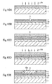
- Cross-sectional diagrams illustrating the semiconductor thin-film manufacturing method of embodiment 1 are shown in Figs. 1A through 1D.
- a silicon oxide film (first insulating film) 2 is first formed on a glass substrate 1, as depicted in Fig. 1A.
- Methods for forming the silicon oxide film 2 on the glass substrate 1 include vapor deposition methods such as Plasma Enhanced Chemical Vapor Deposition (PECVD), Low Pressure Chemical Vapor Deposition (LPCVD), sputtering, and the like.
- PECVD Plasma Enhanced Chemical Vapor Deposition
- LPCVD Low Pressure Chemical Vapor Deposition
- sputtering and the like.
- a silicon oxide film 2 having a thickness of 100 nm can be formed by means of the PECVD method, for example.
- a first amorphous silicon film 3 is then formed on the silicon oxide film 2.
- Methods that can be employed to form the first amorphous silicon film 3 on the silicon oxide film 2 include PECVD, LPCVD, Atmospheric Pressure Chemical Vapor Deposition (APCVD), and sputtering.
- a first amorphous silicon film 3 having a thickness of 50 nm can be formed by means of the LPCVD method, for example.
- a silicon oxide film (second insulating film) 4 is then formed on the first amorphous silicon film 3.
- the silicon oxide film 4 may be fabricated according to the same manufacturing process as the silicon oxide film 2.
- a silicon oxide film 4 having a thickness of 500 nm can be formed by means of the PECVD method, for example.
- a through-hole H is then formed at a prescribed location in the silicon oxide film 4.
- a circular through-hole H whose circular cross-section has a diameter of 0.5 ⁇ m can be formed at a prescribed location within the surface of the silicon oxide film 4 by photolithography and etching, for example. Etching methods can be carried out by means of reactive ion etching that uses plasma of CF 4 gas and H 2 gas, for example.
- An amorphous silicon film 5 is then formed inside the through-hole H in the silicon oxide film 4, as depicted in Fig. 1B.
- a second amorphous silicon film 5 having a prescribed thickness ranging from 50-500 nm can be formed on the silicon oxide film 4 and within the through-hole H by LPCVD, for example.
- the amorphous silicon film 5 is preferably formed by LPCVD, so as to easily and reliably deposit a high-purity silicon film within the through-hole H.
- the second amorphous silicon film 4 is then partially melted by irradiating a laser thereon, as depicted in Fig. 1C. Partial melting can be achieved by irradiation with a XeCl pulse excimer laser (wavelength: 308 nm, pulse duration: 30 nsec) at an energy density of 0.4-1.5 J/cm 2 (corresponding to an amorphous silicon film 4 thickness of 50-500 nm, and preferably 50-250 nm).
- the irradiated XeCl pulse excimer laser is almost completely absorbed near the surface of the amorphous silicon film 5. This is because the absorption coefficients of the amorphous silicon and crystalline silicon for the wavelength (308 nm) of the XeCl pulse excimer laser are large, each being 0.139 nm -1 and 0.149 nm -1 , respectively. Also, the silicon oxide film 4 is substantially transparent with respect to laser, and is not melted by the laser irradiation because of the resultant lack of laser energy absorption therein.
- the second amorphous silicon film 5 reaches a completely-melted state, and the first amorphous silicon film 3 reaches a partially melted state.
- the solidification of silicon following laser irradiation begins first with the first amorphous silicon film 3 and proceeds via the through-hole H in the silicon oxide film 4 towards the completely-melted second amorphous silicon film 5. Crystal grains that have passed via the through-hole H in the silicon oxide film 4 thus act as nuclei for crystal formation during solidification of the completely-melted second amorphous silicon film 5.
- this substantially monocrystalline silicon film 5a Few defects exist within this substantially monocrystalline silicon film 5a, and effects are obtained with respect to the semiconductor film electrical properties thereof such that the trap density near the mid gap of the forbidden bands in the energy bands is reduced. Effects are also obtained such that barriers to the flow of carriers such as electrons and holes are greatly reduced due to the absence of grain boundaries.
- this silicon film 5a is used in the active layer (source/drain area and channel formation area) of a thin-film transistor, a high-grade transistor is obtained having a low off-current value and high mobility.
- FIG. 2 is a plan view of a semiconductor device (thin-film transistor) manufactured in the present embodiment; and Figs. 3A through 3D are cross-sectional diagrams corresponding to a cross-section at line A-A in Fig. 2. In addition, Figs. 1A through 1D are cross-sectional diagrams corresponding to a cross-section at line B-B in Fig. 2.
- a silicon film containing the substantially monocrystalline silicon film 5a is first patterned, and a semiconductor region (semiconductor film) 5b used for a thin-film transistor T is formed as depicted in Fig. 3A.
- a semiconductor region (semiconductor film) 5b used for a thin-film transistor T is formed as depicted in Fig. 3A.
- a silicon oxide film 10 is then formed on the silicon oxide film 4 and the silicon film 5a, as depicted in Fig. 3B.
- the silicon oxide film 10 can be formed according to the electron cyclotron resonance PECVD method (ECR-CVD method) or the PECVD method, for example.
- ECR-CVD method electron cyclotron resonance PECVD method
- PECVD method PECVD method
- This silicon oxide film 10 functions as a gate insulating film for a thin-film transistor.
- a gate electrode 6 is then formed by patterning after forming a tantalum or aluminum metallic thin-film by sputtering, as depicted in Fig. 3C. Impurity ions acting as donors or acceptors are then introduced using this gate electrode 6 as a mask, and the source/drain area 7 and channel formation area 8 are made self-aligning with respect to the gate electrode 6.
- phosphorus (P) as an impurity element is introduced into the source/drain area at a concentration of 1 ⁇ 10 16 cm -2 .
- the impurity element is subsequently activated by irradiation with a XeCl excimer laser at an irradiation energy density of approximately 400 mJ/cm 2 , or by heat treating at approximately 250-450°C.
- a silicon oxide film 12 is then formed on the upper surface of the silicon oxide film 10 and the gate electrode 6, as depicted in Fig. 3D.
- a silicon oxide film 9 of approximately 500 nm is formed by the PECVD method, for example.
- a contact hole C leading to the source/drain area 7 is then opened in the silicon oxide films 10 and 12, and aluminum is deposited in the contact hole C and in the rim of the contact hole C on the silicon oxide film 12 to form a source/drain area 13. Meanwhile, a contact hole leading to the gate electrode 6 is opened in the silicon oxide film 12 to form a terminal electrode 14 (see Fig. 2) used for the gate electrode 6.
- a thin-film transistor T as the semiconductor device of the present invention can thus be manufactured.
- the cross-sectional size of the through-hole H may be equal to or slightly less than a single crystal grain of the polycrystal that forms the first amorphous silicon film 3; and the thickness of the silicon oxide film 4 in which the through-hole H is opened may be approximately the same as the cross-sectional size of the through-hole H.
- the cross-sectional size of the through-hole H can be enlarged beyond the size of a hole formed according to the conventional method.
- the thin-film transistor T is formed by utilizing the area not containing the through-hole H in the surface of the substantially monocrystalline silicon film 5a as the semiconductor thin film 5b in the method of this embodiment, rather than the aforementioned area in which deformities and flaws tend to occur, as depicted in Fig. 2.
- the semiconductor thin film at a separate location from the through-hole in the semiconductor device of the present invention; however, because patterning is performed for the semiconductor thin film of the semiconductor device after the substantially monocrystalline silicon film is formed, the through-hole and the semiconductor thin film are often not connected by the substantially monocrystalline silicon film in the completed semiconductor device. Specifically, the through-hole remains in the vicinity of the semiconductor device as a byproduct of semiconductor manufacturing.
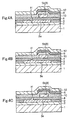
- the substantially monocrystalline silicon is etched down to the inside of the through-hole H and removed during etching of the substantially monocrystalline silicon film 5a, as depicted in Fig. 4A, the silicon fills inside the through-hole H by the silicon oxide film 10.
- Some of the remaining substantially monocrystalline silicon packed inside the through-hole H may be filled by silicon oxide, as depicted in Fig. 4B, according to the etching strength of the substantially monocrystalline silicon film 5a.
- the substantially monocrystalline silicon could be etched down to the surface of the second silicon oxide film just as if back-etched, such that the inside of the through-hole H is in a state similar to having been filled with substantially monocrystalline silicon, as further depicted in Fig. 4C.
- the manner in which the substantially monocrystalline silicon thus remains inside the through-hole H may be determined according to subsequent etching processing and the like. This consideration also applies to the following embodiments.
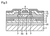
- FIG. 5 A cross-sectional diagram of a thin-film transistor formed according to the semiconductor device manufacturing method of embodiment 2 of the present invention is depicted in Fig. 5.
- the semiconductor device manufacturing method of the present embodiment 2 is fundamentally identical to the semiconductor thin-film and semiconductor device manufacturing method of embodiment 1. However, the method of embodiment 2 differs in that a silicon nitride film 20 is formed on a glass substrate 1 before the silicon oxide film 2 is formed on the glass substrate 1 in embodiment 1, as depicted in Fig. 1A.
- Methods that can be employed to form the silicon nitride film 20 include PECVD, LPCVD, Atmospheric Pressure Chemical Vapor Deposition (APCVD), and sputtering.
- a silicon nitride film 20 having a thickness of 50 nm can be formed by LPCVD, for example.
- the silicon oxide film 2 is formed on the silicon nitride film 20 in the same manner as in embodiment 1, and a first amorphous silicon film 3 is formed on the silicon oxide film 2. Because the these film manufacturing methods and other manufacturing methods are identical to those of embodiment 1, description thereof is omitted.
- the film thickness of the silicon oxide film 2 may, for example, be 100 nm-10 ⁇ m, and preferably 100 nm-200 nm.
- the insulating film shields the substrate from the heat generated during laser heat treatment even better than in the method of embodiment 1, yielding less heat damage to the substrate in addition to achieving the same effects as embodiment 1, because the insulating film directly above the glass substrate 1 has a dual-layered composition comprising the silicon nitride film 20 and the silicon oxide film 2.
- the glass substrate contains impurities that are undesirable for a semiconductor film, such sodium, aluminum, boron, and the like, new effects are achieved such that the diffusion of these impurities from the substrate into the semiconductor film is effectively prevented by providing a dual-layered composition to the insulating layer above the substrate.
- the risk increases of the substrate sustaining extensive heat damage because the laser heat treatment is carried out in the present invention under conditions in which the second amorphous silicon film is completely melted; however, this heat damage is reduced by means of the present embodiment 2 by providing a dual-layered composition to the insulating layer above the substrate.
- This heat damage-reducing effect and the aforementioned impurity diffusion-preventing effect yield a thin-film transistor having exceptional characteristics.
- silicon crystal growth on the second insulating film it is preferable with regard to silicon crystal growth on the second insulating film to make the surface of the second insulating film flat, such that crystal nuclei do not form in the melted amorphous silicon film in the present invention.
- the surface flatness of silicon oxide film is better than that of silicon nitride film when comparing silicon oxide film to silicon nitride film. Because of this, effects are achieved such that crystals are less likely to form in the melted amorphous silicon film, because a silicon oxide film having good surface flatness is formed as a first insulating film, and a silicon nitride film between the first insulating film and the substrate is formed as a second insulating film in the present second embodiment.
- Embodiment 3 of the present invention employs the semiconductor thin-film manufacturing method of the abovementioned method 2.
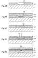
- Cross-sectional diagrams illustrating the semiconductor thin-film manufacturing method of embodiment 3 of the present invention are shown in Figs. 6A through 6D.
- a silicon nitride film (first insulating film) 21 is first formed on a glass substrate 1, as depicted in Fig. 6A.
- a silicon nitride film 21 having a thickness of 2 ⁇ m can be formed by PECVD, for example.
- a silicon oxide film 4 is then formed on the silicon nitride film 21.
- a silicon oxide film 4 having a thickness of 500 nm can be formed by PECVD, for example.
- a photoresist film is then formed on the silicon oxide film 4 in this state, a resist pattern having a through-hole at a prescribed location is formed by photolithography, a through-hole H is first opened at a prescribed location in the surface of the silicon oxide film 4 by dry etching with the resist pattern as a mask, and a concave portion 22 is subsequently formed in the silicon nitride film 21 therebelow.
- Etching for opening the through-hole H in the silicon oxide film 4 may be performed in the same manner as in embodiment 1.
- Etching can be performed by a RIE (Reactive Ion Etching) method using CF 4 as an etching gas, for example.
- Etching for forming the concave portion 22 in the silicon nitride film 21 can be performed by a CDE (Chemical Dry Etching) method using NF 3 and Cl 2 as etching gases, for example.
- the through-hole H may be designed in a substantially uniform columnar shape having a cross-sectional circular diameter of 0.5 ⁇ m; and the cross-sectional surface of the concave portion 22 can be designed to gradually enlarge from directly below the through-hole H, such that the cross-sectional circular diameter of the bottom part is larger (about three times larger, for example) than the cross-sectional circular diameter of the through-hole H.
- Fig. 6A depicts this configuration.
- An amorphous silicon film 5 is then formed on the silicon oxide film 4 by depositing amorphous silicon on the silicon oxide film 4 and in the through-hole H and concave portion 22, as depicted in Fig. 6B.
- the amorphous silicon film 5 is thus formed. It is preferable to use the LPCVD method for the amorphous silicon film 5, because high-purity silicon can thus be deposited easily and reliably within the through-hole H and concave portion 22.
- the amorphous silicon film 5 can thus be formed at a prescribed thickness ranging, for example, from 50 nm-500 nm, and preferably 50 nm-250 nm.
- the amorphous silicon film 5 is then irradiated with a laser to induce melting thereof in the same manner as in embodiment 1, as depicted in Fig. 6C.
- Laser irradiation may be performed using a XeCl pulse excimer laser (wavelength of 308 nm, pulse duration of 30 nsec) at an energy density of 0.4-1.5 J/cm 2 (corresponding to an amorphous silicon film 5 thickness of 50 nm-500 nm), for example.
- the amorphous silicon film 5 reaches a completely-melted state, and the amorphous silicon in the concave portion 22 reaches a partially melted state.
- the solidification of silicon following laser irradiation begins first with the amorphous silicon in the concave portion 22 and proceeds via the through-hole H in the silicon oxide film 4 towards the completely-melted amorphous silicon film 5a. Crystal grains that have passed via the through-hole H in the silicon oxide film 4 thus act as nuclei for crystal formation during solidification of the completely-melted second amorphous silicon film 5a.
- a thin-film transistor can be manufactured according to the same method as the semiconductor device manufacturing method of embodiment 1 using this silicon film 5a.
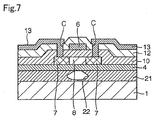
- Fig. 7 depicts a cross-sectional diagram of a thin-film transistor formed by this semiconductor device manufacturing method.
- the concave portion 22 is depicted in a location directly below the thin-film transistor in Fig. 7 for the sake of simplicity, but the concave portion 22 is not limited to being located directly below the thin-film transistor, and may be provided at any location.
- this thin-film transistor has a small off-current value, steeper subthreshold characteristics (smaller subthreshold swing value), higher mobility, and exceptionally high-performance.
- the cross-sectional size of the through-hole H may be the same size as or slightly smaller than the size of a single crystal grain of the polycrystal formed in the amorphous silicon within the concave portion 22; and the thickness of the silicon oxide film 4 in which the through-hole H is opened may also be approximately the same as the cross-sectional size of the through-hole H.
- the cross-sectional size of the through-hole H can be enlarged beyond the size of a hole formed according to the conventional method.
- manufacturing costs can be reduced even further than in the method of embodiment 1, due to the fact that the amorphous silicon film formation process is performed only once.
- Embodiment 4 of the present invention employs the semiconductor thin-film manufacturing method of the abovementioned third method.
- Cross-sectional diagrams illustrating the semiconductor thin-film manufacturing method of embodiment 4 of the present invention are shown in Figs. 8A-8D.
- a silicon nitride film (first insulating film) 21 is first formed on a glass substrate 1, as depicted in Fig. 8A.
- the silicon nitride film 21 is formed by the same method as in embodiment 3.
- a silicon nitride film 21 having a thickness of 300 nm can be formed by PECVD, for example.
- a concave portion 23 is then formed at a prescribed location within the surface of the silicon nitride film 21 by photolithography and etching.
- the cross-section of the concave portion 23 can, for example, be a circular cylinder with a circular cross-sectional diameter of 3 ⁇ m and a depth of 100 nm.
- amorphous silicon film 5d is then formed on the silicon nitride film 21, as depicted in Fig. 8B.
- the amorphous silicon film 5d can be formed by LPCVD, for example. Formation of the amorphous silicon film 5d is performed until amorphous silicon is deposited throughout the inside of the concave portion 23, and until amorphous silicon is deposited on the surrounding film surface of the concave portion 23 of the silicon nitride film 21.
- the amorphous silicon film 5d is then etched as depicted in Fig. 8C, leaving only the amorphous silicon film 5d within the concave portion 23 of the silicon nitride film 21 and exposing the surface of the silicon nitride film 21 other than that of the concave portion 23.
- the amorphous silicon film 5d formed in the concave portion 23 is partially melted by means of subsequent laser irradiation, and is converted to polycrystalline silicon.
- a silicon oxide film 4 is then formed on the silicon nitride film 21, as depicted in Fig. 8D.
- a silicon oxide film 4 having a thickness of 500 nm is formed by the same method as in the aforementioned first embodiment, for example.
- a through-hole H is then formed in the portion corresponding to the concave portion 23 of the silicon oxide film 4.
- a through-hole H having a cross-sectional circular diameter of 0.5 ⁇ m can be formed in the center of the concave portion 23 within the surface of the silicon oxide film 4 by photolithography and etching, for example.
- An amorphous silicon film 5 is then formed on the silicon oxide film 4 and inside the through-hole H, as depicted in Fig. 8E.
- the amorphous silicon film is then partially melted by irradiating a laser on the amorphous silicon film 5 according to the same method as in the aforementioned embodiment 3.
- the amorphous silicon film 5d within the concave portion 23 partially melts and polycrystallizes, crystal growth is induced from a single crystal grain of this polycrystal, and a substantially monocrystalline silicon film can thus be formed.
- a thin-film transistor can be manufactured using this substantially monocrystalline silicon film by the same method as the semiconductor device manufacturing method of embodiment 1.
- Fig. 9 shows a cross-sectional diagram of a thin-film transistor formed according to this semiconductor device manufacturing method.
- the concave portion 23 is depicted in a location directly below the thin-film transistor in Fig. 9 for the sake of simplicity, but the concave portion 23 is not limited to being located directly below the thin-film transistor, and may be provided at any location.
- the cross-sectional size of the through-hole H may be the same size as or slightly smaller than the size of a single crystal grain of the polycrystal formed in the amorphous silicon within the concave portion 23; and the thickness of the silicon oxide film 4 in which the through-hole H is opened may also be approximately the same as the cross-sectional size of the through-hole H.
- the cross-sectional size of the through-hole H can be enlarged beyond the size of a hole formed according to the conventional method.
- the shape of the concave portion formed in the first insulating film is also even easier to control than in the aforementioned embodiment 3, yielding the advantage of being able to easily deposit amorphous silicon in the concave portion.
- Embodiment 5 of the present invention employs the semiconductor thin-film manufacturing method of the abovementioned method 4.
- Cross-sectional diagrams illustrating the semiconductor thin-film manufacturing method of embodiment 5 of the present invention are shown in Figs. 10A-10E.
- the manufacturing method of the present embodiment may be substantially identical to that of the aforementioned first embodiment.
- a silicon oxide film 2 is first formed on a glass substrate 1, as depicted in Fig. 10A.
- Examples of methods for forming the silicon oxide film 1 on the glass substrate 1 include Plasma Enhanced Chemical Vapor Deposition (PECVD), Low Pressure Chemical Vapor Deposition (LPCVD), sputtering, and other vapor-phase deposition techniques.
- PECVD Plasma Enhanced Chemical Vapor Deposition
- LPCVD Low Pressure Chemical Vapor Deposition
- sputtering and other vapor-phase deposition techniques.
- a silicon oxide film 2 having a thickness of 200 nm can be formed by PECVD, for example.
- An amorphous silicon film 3 is then formed on the silicon oxide film 2.
- Methods that can be employed to form the amorphous silicon film 3 on the silicon oxide film 2 include PECVD, LPCVD, Atmospheric Pressure Chemical Vapor Deposition (APCVD), sputtering, and the like.
- An amorphous silicon film 3 having a thickness of 50 nm can be formed by LPCVD, for example.
- the amorphous silicon film 3 is converted to a polycrystalline silicon film 3b by performing laser irradiation R1 on the amorphous silicon film 3.
- Laser irradiation is performed using XeCl pulse excimer laser (wavelength: 308 nm, pulse duration: 30 nsec) having an energy density from approximately 0.3 J/cm 2 to 0.5 J/cm 2 .
- Laser irradiation R1 may also be performed approximately 20 times for the same location on the amorphous silicon film 3.
- the amorphous silicon film 3 can be converted to a polycrystalline silicon film 3b having a crystal orientation (111) within the film surface thereof by performing laser irradiation R1 repeatedly in the same location, as described in "Laser Processing of Amorphous for Large-area Polysilicon Imagers.” (J. B. Boyce et al., Thin Solid Films, vol. 383 (2001) pp. 137-142).
- a silicon oxide film 4 is then formed on the polycrystalline silicon film 3b, as depicted in Fig. 10B.
- a silicon oxide film 4 having a thickness ranging from 500 nm to 2 ⁇ m can be formed on the polycrystalline silicon film 3b by PECVD, for example.
- a through-hole H is then formed in the silicon oxide film 4.
- a substantially circular through-hole H whose cross-section has a diameter of approximately 50 nm to 500 nm can be formed at a prescribed location within the surface of the silicon oxide film 4 by photolithography and etching, for example. This etching can be performed by means of reactive ion etching that uses plasma of CF 4 gas and CHF 3 gas, for example.
- An amorphous silicon film 5 is then formed on the silicon oxide film and inside the through-hole H, as depicted in Fig. 10C.
- LPCVD LPCVD
- a high-purity amorphous silicon film 5 can easily be deposited on the silicon oxide film 4 while the amorphous silicon film 5 is reliably filled inside the through-hole H.
- Laser irradiation R2 is then performed for the amorphous silicon film 5 deposited on the silicon oxide film 4, as depicted in Fig. 10D.
- laser irradiation R2 is performed using XeCl pulse excimer laser (wavelength of 308 nm, pulse duration of 30 nsec) with an energy density from approximately 0.4 J/cm 2 to 1.5 J/cm 2 that is suitable for the amorphous silicon film 5 having a thickness of 50 nm to 500 nm, and preferably of 50 nm to 250 nm.
- the XeCl pulse excimer laser irradiated to the amorphous silicon film 5 is almost completely absorbed near the surface of the amorphous silicon film 5. This is because the absorption coefficients of the amorphous silicon and crystalline silicon for the wavelength (308 nm) of the XeCl pulse excimer laser are large, each being 0.139 nm -1 and 0.149 nm -1 , respectively.
- the amorphous silicon film 5 can be brought to a completely-melted state while the polycrystalline silicon film 3b under the silicon oxide film 4 is preserved in the unmelted or partially melted state.
- the solidification of the silicon following laser irradiation R2 can thus be directed to proceed first from the polycrystalline silicon film 3b, via the through-hole H of the silicon oxide film 4, and on to the completely-melted amorphous silicon film 5. Crystal growth then occurs in the completely-melted amorphous silicon film 5 at the time of solidification, with the crystal grains that have passed via the through-hole H of the silicon oxide film 4 acting as nuclei.
- the crystal orientation of one of the numerous crystal grains contained in the polycrystalline silicon film 3b can be transferred to the amorphous silicon film 5 via the through-hole H, inducing crystal growth on the silicon oxide film 4, with this crystal grain acting as the nucleus thereof, by setting the cross-sectional dimensions of the through-hole H to be the same size or slightly smaller than one of the numerous crystal grains contained in the polycrystalline silicon film 3b.
- a thin-film transistor can be manufactured using this silicon film 5a by the same method as the semiconductor device manufacturing method of embodiment 1.
- Fig. 11 shows a cross-sectional diagram of a thin-film transistor formed according to this semiconductor device manufacturing method.
- the polycrystalline silicon film 3b Before the silicon oxide film 4 is formed on the polycrystalline silicon film 3b, the polycrystalline silicon film 3b may be processed by photolithography or etching such that only portions thereof in the vicinity of the through-hole H are left remaining.
- Embodiment 6 of the present invention relates to a modified example of the semiconductor thin-film manufacturing method of the above-mentioned method 4.
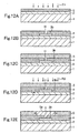
- Cross-sectional diagrams illustrating the semiconductor thin-film manufacturing method of embodiment 6 of the present invention are shown in Figs. 12A through 12E.
- the present embodiment 6 is substantially identical to the aforementioned embodiment 5. However, the present embodiment differs from embodiment 5, in that after the amorphous silicon film 3 is converted to a polycrystalline silicon film 3b, the silicon oxide film 4 is provided after the polycrystalline silicon film 3b has been patterned in a prescribed shape.
- the amorphous silicon film 3 is converted to a polycrystalline silicon film 3b by performing laser irradiation R1 on the amorphous silicon film 3.
- the polycrystalline silicon film 3b is then patterned by photolithography and etching.
- a silicon oxide film 4 is then formed on the polycrystalline silicon film 3b by PECVD, for example, as depicted in Fig. 12B; and a through-hole H is formed at a prescribed location in the silicon oxide film 4 on the polycrystalline silicon film 3b by photolithography and etching, for example.
- An amorphous silicon film 5 is then deposited onto the silicon oxide film 4 using the LPCVD method, for example, so as to fill the inside of the through-hole H, as depicted in Fig. 12C.
- the amorphous silicon film 5 is then brought to a completely-melted state while the unmelted or partially melted state of the polycrystalline silicon film 3b is preserved by performing laser irradiation R2 on the amorphous silicon film 5 deposited onto the silicon oxide film 4, as depicted in Fig. 12D.
- the amorphous silicon film 5 then solidifies after laser irradiation R2, as depicted in Fig. 12E, and a substantially monocrystalline silicon film 5a is formed in the area of the surface of the amorphous silicon film 5 centered around the through-hole H.
- a thin-film transistor can be manufactured using this silicon film 5a according to the same method as the semiconductor device manufacturing method of embodiment 1.
- Fig. 13 depicts a cross-sectional diagram of a thin-film transistor formed by this semiconductor device manufacturing method.
- the polycrystalline silicon film 3b is depicted in a location directly below the thin-film transistor in Fig. 13 for the sake of simplicity, but the polycrystalline silicon film 3b is not limited to being located directly below the thin-film transistor, and may be provided at any location.
- a through-hole H is formed in the silicon oxide film 4 disposed between the two layers comprising amorphous silicon films 3 and 5, and irregularities in crystal orientation that occur in the conventional method can be reduced by designing the amorphous silicon film 3 facing the glass substrate 1 to be a polycrystalline silicon film 3b having a substantially coordinated crystal orientation.
- Fig. 14 depicts a cross-sectional diagram of a thin-film transistor formed according to the semiconductor device manufacturing method according to embodiment 7 of the present invention.
- the semiconductor device manufacturing method of the present embodiment 7 is fundamentally identical to the semiconductor thin-film and semiconductor device manufacturing method of embodiment 6. However, the method of embodiment 7 differs in that a silicon nitride film 20 is formed on the glass substrate 1 before the silicon oxide film 2 is formed on the glass substrate 1 in embodiment 6 in the manner depicted in Fig. 12A.
- the silicon nitride film 20 is formed on the glass substrate 1 in Fig. 14 by a vapor deposition method such as Plasma Enhanced Chemical Vapor Deposition (PECVD), Low Pressure Chemical Vapor Deposition (LPCVD), sputtering, or the like.
- PECVD Plasma Enhanced Chemical Vapor Deposition
- LPCVD Low Pressure Chemical Vapor Deposition
- sputtering or the like.
- a silicon oxide film 2, polycrystalline silicon film 3b, and a silicon oxide film 4 are then formed sequentially on the silicon nitride film 20 in the same manner as in the configuration depicted in Fig. 12D, and a substantially monocrystalline silicon film 5a is formed on the silicon oxide film 4.
- a gate electrode 6 is then formed via the silicon oxide film 10 in the area 5b not occupied by the through-hole H of the substantially monocrystalline silicon film 5a, and a source/drain area 7 is formed in the semiconductor thin film 5b on both sides of the gate electrode 6.
- a source/drain electrode 13 and a terminal electrode 14 for gate electrode use is also formed on the gate electrode 6 via the silicon oxide film 12 such that the source/drain electrode 13 is connected with the source/drain area 7 via a contact hole C, and the terminal electrode 14 for gate electrode use is connected with the gate electrode 6 via another contact hole.
- the film thickness of the silicon nitride film 20 in this step can, for example, be 50 nm, and the film thickness of the silicon oxide film 2 can, for example, be 100 nm-200 nm.
- the same effects as in embodiment 1 are achieved by means of embodiment 7 described above. Specifically, the effect of the insulating film shielding the glass substrate 1 from heat generated during laser irradiation R1 and R2 can be enhanced, and heat damage to the glass substrate 1 can be minimized by forming the silicon oxide film 2 after forming the silicon nitride film 20 on the glass substrate 1, because the insulating film directly above the glass substrate 1 is thus provided with a dual-layered composition comprising the silicon nitride film 20 and the silicon oxide film 2.
- the glass substrate 1 contains impurities that are undesirable for a semiconductor film, such as sodium, aluminum, boron, and the like, the diffusion of these impurities from the substrate into the semiconductor film is effectively prevented by providing the insulating layer above the glass substrate 1 with a dual-layered composition according to the present embodiment.
- Another feature of the present embodiment is that a thin-film transistor having exceptional characteristics can easily be obtained by means of these heat damage-reducing effects and impurity diffusion-preventing effects. It is also preferable with regard to silicon crystal growth on the silicon oxide film 4 to make the surface of the silicon oxide film 4 flat to prevent crystal nuclei from forming in the melted amorphous silicon film.
- the surface flatness of the silicon oxide film 2 is better than that of the silicon nitride film 20 when the silicon oxide film 2 and the silicon nitride film 20 are compared. Because of this, it is more preferable to form silicon oxide films 2 and 4 having good surface flatness as insulating films directly under the amorphous silicon films 3 and 5, and to form a silicon nitride film 20 between the silicon oxide film 2 and the glass substrate 1.
- a method for providing an insulating film with a dual-layered composition to minimize heat damage to the glass substrate 1 during laser irradiation R2 was described in the present embodiment, but the insulating film may also be provided with a composition having three or more layers.
- Embodiment 8 of the present invention relates to an electro-optical device provided with a semiconductor device or the like manufactured according to the semiconductor device manufacturing method of the present invention.
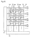
- Fig. 15 is a connection diagram of the electrooptic (display) device 100 according to embodiment 8.
- the display device 100 of the present embodiment comprises a luminescent layer OELD capable of emitting light as a result of electroluminescent effect in pixel areas G, and a retention capacitance C for storing an electrical current for driving the luminescent layer.
- the semiconductor device is manufactured according to the manufacturing method of the present invention, and thin-film transistors T1-T4 are provided therein.
- Scan lines Vsel and luminescence control lines Vgp are supplied to each pixel area G from a driver area 101.
- Data lines Idata and power supply lines Vdd are supplied to each pixel area G from a driver area 102.
- An electrical current program for each pixel area G is executed, and the luminescence from the luminescent unit OELD can be controlled by controlling the scan lines Vsel and the data lines Idata.
- the semiconductor thin film provided in the semiconductor device has few internal defects, the electrical properties of the semiconductor film thereof exhibit a reduced trap density near the mid gap of the forbidden bands in the energy bands, and the semiconductor device is high-grade and has a small off-current value and high mobility due to the fact that barriers to the flow of carriers such as electrons and holes are greatly reduced by the absence of grain boundaries.
- the drive circuit described above is an example of a circuit employing electroluminescent elements as luminescent elements, but other circuit configurations are also possible.
- applying the semiconductor device manufacturing method to the driver area 101 or 102 or employing liquid crystal display elements as luminescent elements could also be possible by modifying the circuit configuration in various ways.
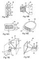
- the present embodiment 9 relates to an electronic appliance comprising a semiconductor device and other components manufactured according to the semiconductor device manufacturing method of the present invention. Examples of electronic appliance of embodiment 9 are cited in Figs. 16A through 16F.
- Fig. 16A depicts an example of a portable telephone that is equipped with a semiconductor device and other components manufactured according to the manufacturing method of the present invention, wherein the portable telephone 30 comprises an electro-optical device (display panel) 31, a sound output component 32, a sound input component 33, an operating component 34, and an antenna component 35.
- the semiconductor device manufacturing method of the present invention is applied to the manufacture of the semiconductor devices disposed in the display panel 31 or internal circuits, for example.
- Fig. 16B depicts an example of a video camera that is equipped with a semiconductor device or the like manufactured according to the manufacturing method of the present invention, wherein the video camera 40 comprises an electro-optical device (display panel) 41, an operating component 42, a sound input component 43, and an image receiving component 44.
- the semiconductor device manufacturing method of the present invention is applied to the manufacture of the semiconductor devices disposed in the display panel 41 or internal circuits, for example.
- Fig. 16C depicts an example of a personal computer that is equipped with a semiconductor device or the like manufactured according to the manufacturing method of the present invention, wherein the computer 50 comprises an electro-optical device (display panel) 51, an operating component 52, and a camera component 53.
- the semiconductor device manufacturing method of the present invention is applied to the manufacture of the semiconductor devices disposed in the display panel 51 or internal circuits, for example.
- Fig. 16D depicts an example of a head mount display that is equipped with a semiconductor device or the like manufactured according to the manufacturing method of the present invention, wherein the head mount display 60 comprises an electro-optical device (display panel) 61, an optical system housing 62, and a band component 63.
- the semiconductor device manufacturing method of the present invention is applied to the manufacture of the semiconductor devices disposed in the display panel 61 or internal circuits, for example.
- Fig. 16E depicts an example of a rear projector that is equipped with a semiconductor device or the like manufactured according to the manufacturing method of the present invention, wherein the projector 70 comprises an electro-optical device (optical modulator) 71, a light source 72, an integrated optical system 73, mirrors 74 and 75, and a screen 77 inside a case 76.
- the semiconductor device manufacturing method of the present invention is applied to the manufacture of the semiconductor devices disposed in the optical modulator 71 or internal circuits, for example.
- Fig. 16F depicts an example of a front projector that is equipped with a semiconductor device or the like manufactured according to the manufacturing method of the present invention, wherein the projector 80 is capable of displaying images onto a screen 84, and comprises an electro-optical device (image display source) 81 and an optical system 82 inside a case 83.
- the semiconductor device manufacturing method of the present invention is applied to the manufacture of the semiconductor devices disposed in the image display source 81 or internal circuits, for example.
- the semiconductor device manufacturing method pertaining to the present invention is not limited to the examples described above, and can be applied to the manufacture of all types of electronic appliance. Additional application can be made to a display-equipped fax device, digital camera viewfinder, portable TV, DSP device, PDA, electronic notebook, electric signboard, advertising display, IC card, or the like.
- the semiconductor thin film provided in the semiconductor device has few internal defects, the electrical properties of the semiconductor film thereof exhibit a reduced trap density near the mid gap of the forbidden bands in the energy bands, and the semiconductor device is high-grade and has a small off-current value and high mobility due to the fact that barriers to the flow of carriers such as electrons and holes are greatly reduced by the absence of grain boundaries.
- the diameter of the through-hole in the insulating film may be the same size or slightly smaller than the size of a single crystal grain that comprises the polycrystal formed on the layer of silicon film below the insulating film, because an insulating film having a through-hole between two layers of silicon film is provided, the silicon film is partially melted by irradiating a laser thereon, and a substantially monocrystalline film is continuously formed extending via the through-hole from at least part of the layer of silicon film below the insulating film (that continues via the through-hole) to at least part of the layer of silicon film above the insulating film. Costly precision exposure devices and etching devices are therefore unnecessary. Numerous high-performance semiconductor devices can also be formed easily on a large glass substrate, as in large liquid-crystal displays and the like.
- a high-performance semiconductor device having a small off-current value, steep subthreshold characteristics, and high mobility can thus be obtained because a substantially monocrystalline silicon film is provided to the semiconductor device, integrated circuit, and electronic appliance of the present invention.
Landscapes
- Chemical & Material Sciences (AREA)
- Chemical Kinetics & Catalysis (AREA)
- General Chemical & Material Sciences (AREA)
- Engineering & Computer Science (AREA)
- Materials Engineering (AREA)
- Metallurgy (AREA)
- Organic Chemistry (AREA)
- Crystallography & Structural Chemistry (AREA)
- Mechanical Engineering (AREA)
- Recrystallisation Techniques (AREA)
- Thin Film Transistor (AREA)
Abstract
According to the semiconductor thin-film and semiconductor device
manufacturing method of the present invention, an insulating film having a through-hole
between two layers of silicon film is provided, the silicon film is partially melted
by irradiating a laser thereon, and a substantially monocrystalline film is
continuously formed extending via the through-hole from at least part of the layer of
silicon film below the insulating film that continues to the through-hole, to at least
part of the layer of silicon film above the insulating film. It is therefore sufficient to
form a through-hole with a larger diameter than that of a hole formed by the
conventional method, because the diameter of the through-hole in the insulating film
may be the same size or slightly smaller than the size of a single crystal grain that
comprises the polycrystal formed in the silicon film below the insulating film. Costly
precision exposure devices and etching devices are therefore unnecessary.
Numerous high-performance semiconductor devices can also be formed easily on a
large glass substrate, as in large liquid-crystal displays and the like.
Description
The present invention relates to a semiconductor thin film and semiconductor
device manufacturing method, and particularly to an improvement of a
semiconductor thin-film formation method whereby a substantially monocrystalline
silicon film can be formed in a suitable manner.
Methods for manufacturing thin-film semiconductor devices whereby
amorphous silicon films are heat-treated by a laser to form a polycrystalline silicon
film, and the resulting polycrystalline silicon film is used as a semiconductor film to
form gate electrodes and wiring on a thin metal film have been proposed for
manufacturing thin-film semiconductor devices represented by polycrystalline silicon
thin-film transistors (p-Si TFT) at comparatively low temperatures. With these
methods, however, it is difficult to control the energy of laser, and the manufactured
semiconductor films have nonuniform properties, so techniques that are free of
these drawbacks and allow substantially monocrystalline silicon films to be grown
have been proposed instead (see publications "Single Crystal Thin film Transistors,"
IBM Technical Disclosure Bulletin, Aug. 1993, pp. 257-258, and "Advanced
Excimer-Laser Crystallization Techniques of Si Thin-Film For Location Control of
Large Grain on Glass," R. Ishihara et al, Proc. SPIE 2001, vol. 4295, pp. 14-23).
These publications disclose techniques in which a hole is formed in an
insulating film on a substrate, an amorphous silicon film is formed on the insulating
film and in the hole, the amorphous silicon film is irradiated by a laser, and the
amorphous silicon in the bottom portions of the hole is kept in an unmelted state
while the amorphous silicon film on other portions is melted, whereby crystals are
grown using the amorphous silicon in the unmelted state as a crystal nucleus, and a
silicon film in a substantially monocrystalline state is formed.
In the methods formed in these two publications, a plurality of crystal nuclei
form in the bottom portion of the hole if the cross-section of the hole is not made
sufficiently small, so expensive precision exposure devices and etching devices are
needed to form a hole with such a diameter (50 nm to 150 nm).
In addition, hole formation is difficult when these devices are used to form
numerous thin-film transistors on large glass substrates, as is the case with large
liquid-crystal displays and the like.
With the foregoing in view, it is an object of the present invention to form a
semiconductor thin film having an adequate substantially monocrystalline silicon film
without the use of costly precision exposure devices or etching devices.
Aimed at attaining the stated object, the present invention is a semiconductor
thin-film manufacturing method comprising a step for providing an insulating film
having a through-hole between two layers of silicon film; and a step for partially
melting the silicon film by irradiation with a laser, and continuously forming a
substantially monocrystalline film extending via the through-hole from at least part of
the layer of silicon film below the insulating film to at least part of the layer of silicon
film above the insulating film. This method is referred to as the basic method of the
present invention.
In the present invention, an area centered around the through-hole in the
surface of the layer of silicon film above the insulating film is fashioned into a
substantially monocrystalline silicon film by inducing crystal growth, with the nucleus
thereof comprising a single crystal grain from among a plurality of crystal grains
generated in the layer of silicon film below the insulating film, because solidification
of the melted silicon after laser irradiation begins in the layer of silicon film below the
insulating film and proceeds to the layer of silicon film above the insulating film via
the through-hole in the insulating film. It is therefore sufficient to form a through-hole
with a larger diameter than that of a hole formed by the conventional method,
because the diameter of the through-hole in the insulating film may be the same size
or slightly smaller (a diameter of 0.2 µm-1.0 µm, for example) than the size of a
single crystal grain that comprises the polycrystal formed on the layer of silicon film
below the insulating film.
"Substantially monocrystalline" in the present invention includes not only
cases in which crystal grains are singular, but also similar states, such as those in
which a plurality of monocrystals are assembled together, yet are few in number,
thereby providing characteristics that are identical to those of a semiconductor thin
film that is formed in a substantially monocrystalline fashion as far as the
semiconductor thin-film characteristics thereof are concerned.
"Through-hole" in the present invention refers to a passage extending
through the insulating film from above and beneath, with no particular distinction as
to the cross-sectional shape thereof. The "through-hole" also does not necessarily
require a cylindrical shape with a uniform diameter in all parts thereof, and the
cross-sectional diameter may differ in each part.
"Continuously formed" in the present invention denotes crystal growth without
the occurrence of interfacial boundaries.
The present invention is also a semiconductor thin-film manufacturing method
comprising a step for forming a first amorphous silicon film on a first insulating film;
a step for forming a second insulating film on the first amorphous silicon film and
forming a through-hole at a prescribed location in the surface of the second
insulating film; a step for forming a second amorphous silicon film on the second
insulating film by depositing amorphous silicon onto the second insulating film and
into the through-hole; and a step for converting an area centered around the
through-hole in the surface of the second amorphous silicon film into substantially
monocrystalline silicon by irradiating a laser onto the second amorphous silicon film
to bring the second amorphous silicon film to a completely-melted state and the first
amorphous silicon film to a partially melted state. This method is referred to as
method 1 of the present invention.
The present invention is also a semiconductor thin-film manufacturing method
comprising a step for forming a second insulating film comprising a different material
from the first insulating film on a first insulating film; a step for forming a through-hole
at a prescribed location in the surface of the second insulating film; a step for
forming a concave portion with a larger cross-section than the through-hole at the
location of the through-hole in the first insulating film; a step for forming an
amorphous silicon film on the second insulating film by depositing amorphous silicon
onto the second insulating film, into the through-hole, and into the concave portion;
and a step for converting an area centered around the through-hole in the surface of
the amorphous silicon film into substantially monocrystalline silicon by irradiating a
laser onto the amorphous silicon film to bring the amorphous silicon film to a
completely-melted state and the amorphous silicon film in the concave portion to a
partially melted state. This method is referred to as method 2 of the present
invention.
Furthermore, the present invention is also a semiconductor thin-film
manufacturing method comprising a step for forming a concave portion at a
prescribed location in the surface of the first insulating film; a step for depositing
amorphous silicon into the concave portion; a step for forming a second insulating
film on the first insulating film; a step for forming a through-hole with a cross-section
smaller than the concave portion at the location of the concave portion in the second
insulating film; a step for forming an amorphous silicon film on the second insulating
film by depositing amorphous silicon onto the second insulating film and into the
through-hole; and a step for converting an area centered around the through-hole in
the surface of the amorphous silicon film into substantially monocrystalline silicon by
irradiating a laser onto the amorphous silicon film to bring the amorphous silicon film
to a completely-melted state and the amorphous silicon film in the concave portion
to a partially melted state. This method is referred to as method 3 of the present
invention.
The present invention is a semiconductor thin-film manufacturing method
comprising a step for forming a first amorphous silicon film on a first insulating film;
a step for converting the first amorphous silicon film into a polycrystalline silicon film
by laser irradiation to the first amorphous silicon film; a step for forming a second
insulating film on the polycrystalline silicon film; a step for forming a through-hole in
the second insulating film; a step for forming a second amorphous silicon film on the
second insulating film so as to fill the through-hole; and a step for converting the
second amorphous silicon film centered around the through-hole into a substantially
monocrystalline silicon film by irradiating a laser to the second amorphous silicon
film to bring the second amorphous silicon film to a completely-melted state, with the
polycrystalline silicon film remaining in an unmelted or partially melted state. This
method is referred to as method 4 of the present invention.
In method 1 of the present invention, solidification of the silicon after laser
irradiation begins in the first amorphous silicon film and proceeds to the second
amorphous silicon film via the through-hole in the second insulating film.
Consequently, an area centered around the through-hole in the surface of the
second amorphous silicon film becomes a substantially monocrystalline silicon film
due to the occurrence of crystal growth, with the nucleus thereof comprising a single
crystal grain from among numerous crystal grains generated in the first amorphous
silicon film. It is therefore sufficient to form a through-hole with a larger diameter
than that of a hole formed by the conventional method, because the cross-sectional
size of the through-hole in the second insulating film may be the same size or
slightly smaller (a diameter of 0.2 µm-1.0 µm, for example) than the size of a single
crystal grain that comprises the polycrystal formed in the first amorphous silicon film.
The thickness of the second insulating film in which the through-hole is opened may
also be approximately the same size as the cross-sectional size of the through-hole
(the diameter thereof if the cross-section is circular).
In methods 2 and 3 of the present invention, solidification of the silicon after
laser irradiation begins first with the first amorphous silicon in the concave portion,
and proceeds to the completely-melted amorphous silicon film via the through-hole
in the second insulating film. Consequently, an area centered around the through-hole
in the surface of the amorphous silicon film becomes a substantially
monocrystalline silicon film due to the occurrence of crystal growth, with the nucleus
thereof comprising a single crystal grain from among numerous crystal grains
generated in the amorphous silicon in the concave portion. It is therefore sufficient
to form a through-hole with a larger diameter than that of a hole formed by the
conventional method, because the cross-sectional size of the through-hole in the
second insulating film may be the same or slightly smaller (a diameter of
0.2 µm-1.0 µm, for example) than the size of a single crystal grain that comprises
the polycrystal formed in the amorphous silicon in the concave portion. The
thickness of the second insulating film in which the through-hole is opened may also
be approximately the same size as the cross-sectional size of the through-hole (the
diameter thereof if the cross-section is circular).
In method 4 of the present invention, solidification of the silicon after laser
irradiation begins first with the surface of the first amorphous silicon film that is
converted to a polycrystalline silicon film, and proceeds to the completely-melted
amorphous silicon film via the through-hole in the second insulating film.
Consequently, an area centered around the through-hole in the surface of the
amorphous silicon film becomes a substantially monocrystalline silicon film due to
the occurrence of crystal growth, with the nucleus thereof comprising one of the
crystal grains in the polycrystalline silicon film. It is therefore sufficient to form a
through-hole with a larger diameter than that of a hole formed by the conventional
method, because the cross-sectional size of the through-hole in the second
insulating film may be the same or slightly smaller (a diameter of 0.2 µm-1.0 µm, for
example) than the size of a single crystal grain that comprises the polycrystal. The
thickness of the second insulating film in which the through-hole is opened may also
be approximately the same size as the cross-sectional size of the through-hole (the
diameter thereof if the cross-section is circular).
Costly precision exposure devices and etching devices such as those
employed in the conventional method are therefore no longer needed to form minute
holes (through-holes and concave portions) for the purpose of monocrystal growth
according to methods 1-4 of the present invention.
Specifically, the diameter of the through-hole may be the same or slightly
smaller than the size of a single crystal grain contained in the polycrystalline silicon
film according to the semiconductor thin-film manufacturing method of the present
invention.
The first insulating film and second insulating film may comprise silicon oxide
films, and a silicon nitride film may be formed as the layer below the first insulating
film in inventions 1-4 of the present invention.
Furthermore, the first insulating film may be a silicon nitride film, and the
second insulating film may be a silicon oxide film in invention 2 and invention 3 of
the present invention.
Yet furthermore, the present invention may comprise a step for forming a
semiconductor device in which a substantially monocrystalline silicon film
manufactured according to the present inventions described above is used as a
semiconductor thin film.
"Semiconductor device" in the present invention refers to a device provided
with a substantially monocrystalline silicon film, and comprises any single element
such as a transistor, diode, resistor, inductor, capacitor, or other active/passive
element.
In the semiconductor device manufacturing method of the present invention, it
is preferable to form a semiconductor device such that the portion of the
substantially monocrystalline silicon film not containing the through-hole is used as
a semiconductor thin film. This is because the crystal film characteristics are more
stable farther away from the through-hole.
The semiconductor device manufactured according to the semiconductor
device manufacturing method of the present invention is a thin-film transistor, and
the through-hole is disposed according to the location in which the thin-film
transistor is formed.
The semiconductor device manufactured according to the basic method of
the present invention comprises an insulating film having a through-hole; and a
substantially monocrystalline silicon film continuously formed inside the through-hole,
on at least part of the layer below the insulating film extending into the
through-hole, and on at least part of the layer above the insulating film extending
into the through-hole; and uses a substantially monocrystalline silicon film as a
semiconductor thin film.
The semiconductor device manufactured according to method 1 of the
present invention comprises a substantially polycrystalline silicon film as the layer
below the insulating film; and the monocrystalline silicon film is continuously formed
up to the through-hole and layer above the insulating film from at least part of the
polycrystalline silicon film. Specifically, this is because the amorphous silicon film
becomes a polycrystalline silicon film by means of laser irradiation, and the
substantially monocrystalline silicon film is grown from the crystal grains of the
polycrystalline silicon film.
The semiconductor device manufactured according to method 2 or 3 of the
present invention comprises as the layer below the insulating film an insulating film
having a concave portion in the part which continues into the through-hole; and the
substantially monocrystalline silicon film is continuously formed up to the through-hole
and layer above the insulating film from at least part of the concave portion.
Specifically, this is because the substantially monocrystalline silicon film is grown
from a single crystal grain of the polycrystalline silicon formed by laser irradiation.
The semiconductor device manufactured according to method 4 of the
present invention comprises a polycrystalline silicon film as the layer below the
insulating film; and the substantially monocrystalline silicon film is continuously
formed up to the layer above the insulating film, with a crystal grain contained in the
polycrystalline silicon film as the nucleus thereof. Specifically, this is because the
amorphous silicon film is converted to a polycrystalline silicon film by laser
irradiation, and the substantially monocrystalline silicon film grows from one of the
crystal grains thereof.
Specifically, the semiconductor device of the present invention comprises a
polycrystalline silicon film formed on the first insulating film; a second insulating film
with a through-hole formed on the polycrystalline silicon film; and a substantially
monocrystalline silicon film formed on the second insulating film and contiguous with
the polycrystalline silicon film via the through-hole, with crystal grains contained in
the polycrystalline silicon film as nuclei thereof.
The semiconductor device of the present invention comprises a first
insulating film having a concave portion that contains substantially polycrystalline
silicon; a second insulating film having a through-hole in a location continuing to the
concave portion, formed on the first insulating film; and a substantially
monocrystalline silicon film formed on the second insulating film and contiguous with
the polycrystalline silicon film in the concave portion via the through-hole, with
crystal grains contained in the polycrystalline silicon film as nuclei thereof.
In the present invention, the first insulating film and the second insulating film
may be silicon oxide films, and a silicon nitride film may be further formed on the
lower layer of the first insulating film. The silicon nitride film may be formed in any
manner.
The present invention is configured using the portion not containing the
through-hole in the surface of the substantially monocrystalline silicon as a
semiconductor thin film. This is because the crystal film characteristics are more
stable farther away from the through-hole.
The substantially monocrystalline silicon film that comprises the
semiconductor thin film is separated from the through-hole in the present invention.
Specifically, this is because the crystals between the through-hole and the area
utilized as the semiconductor thin film are connected together because
crystallization occurs continuously from the through-hole during manufacture of the
substantially monocrystalline silicon film, but no problems are encountered when the
semiconductor thin film in the through-hole and in the utilized area is separated by
etching or the like following formation of the semiconductor thin film. Therefore,
substantially monocrystalline silicon may or may not exist in the through-hole after
the semiconductor device is manufactured.
The present invention is an integrated circuit, electro-optical device, and
electronic appliance provided with the semiconductor device of the present
invention.
As used herein, "integrated circuit" refers to a circuit (chip) in which a
semiconductor device, interconnected wiring, and the like is integrated and wired to
achieve a specific function.
The present invention comprises a plurality of pixel areas, a semiconductor
device disposed in each pixel area, and electrooptic elements controlled by the
semiconductor devices in an electro-optical device; wherein the semiconductor
device is manufactured according to the semiconductor device manufacturing
method of the present invention.
As used herein, "electro-optical device" refers to a general device provided
with the semiconductor device of the present invention, provided with electro-optical
elements for emitting light by means of electronic action or for altering the conditions
of external light; and includes both devices for independently emitting light, and
devices for controlling the transmission of external light. The electro-optical
elements referred to herein include, for example, liquid crystal elements,
electrophoretic elements having a dispersion medium in which electrophoretic
particles are dispersed, EL (Electroluminescence) elements, active matrix display
devices provided with electron emission elements for emitting light by directing
electrons generated by application of an electric field to an emission substrate, and
the like.
The present invention is also an electronic appliance comprising a
semiconductor device manufactured according to the semiconductor device
manufacturing method of the present invention.
As used herein, "electronic appliance" refers to a general apparatus for
achieving a specific function, comprising the semiconductor device of the present
invention; and is structured from, for example, an electro-optical device and memory
provided therein. The configuration thereof is not particularly limited, and may
comprise an IC card, portable telephone, video camera, personal computer, head
mount display, rear or front projector, a fax device further equipped with display
functionality, digital camera viewfinder, portable TV, DSP device, PDA, electronic
notebook, electric signboard, advertising display, or the like.
Embodiments of the present invention will be described hereafter with
reference to the figures.
A silicon oxide film (first insulating film) 2 is first formed on a glass
substrate 1, as depicted in Fig. 1A. Methods for forming the silicon oxide film 2 on
the glass substrate 1 include vapor deposition methods such as Plasma Enhanced
Chemical Vapor Deposition (PECVD), Low Pressure Chemical Vapor Deposition
(LPCVD), sputtering, and the like. A silicon oxide film 2 having a thickness of
100 nm can be formed by means of the PECVD method, for example.
A first amorphous silicon film 3 is then formed on the silicon oxide film 2.
Methods that can be employed to form the first amorphous silicon film 3 on the
silicon oxide film 2 include PECVD, LPCVD, Atmospheric Pressure Chemical Vapor
Deposition (APCVD), and sputtering. A first amorphous silicon film 3 having a
thickness of 50 nm can be formed by means of the LPCVD method, for example.
A silicon oxide film (second insulating film) 4 is then formed on the first
amorphous silicon film 3. The silicon oxide film 4 may be fabricated according to the
same manufacturing process as the silicon oxide film 2. A silicon oxide film 4 having
a thickness of 500 nm can be formed by means of the PECVD method, for example.
A through-hole H is then formed at a prescribed location in the silicon oxide
film 4. A circular through-hole H whose circular cross-section has a diameter of
0.5 µm can be formed at a prescribed location within the surface of the silicon oxide
film 4 by photolithography and etching, for example. Etching methods can be carried
out by means of reactive ion etching that uses plasma of CF4 gas and H2 gas, for
example.
An amorphous silicon film 5 is then formed inside the through-hole H in the
silicon oxide film 4, as depicted in Fig. 1B. A second amorphous silicon film 5 having
a prescribed thickness ranging from 50-500 nm can be formed on the silicon oxide
film 4 and within the through-hole H by LPCVD, for example. The amorphous silicon
film 5 is preferably formed by LPCVD, so as to easily and reliably deposit a high-purity
silicon film within the through-hole H.
The second amorphous silicon film 4 is then partially melted by irradiating a
laser thereon, as depicted in Fig. 1C. Partial melting can be achieved by irradiation
with a XeCl pulse excimer laser (wavelength: 308 nm, pulse duration: 30 nsec) at an
energy density of 0.4-1.5 J/cm2 (corresponding to an amorphous silicon film 4
thickness of 50-500 nm, and preferably 50-250 nm).
In this step, the irradiated XeCl pulse excimer laser is almost completely
absorbed near the surface of the amorphous silicon film 5. This is because the
absorption coefficients of the amorphous silicon and crystalline silicon for the
wavelength (308 nm) of the XeCl pulse excimer laser are large, each being
0.139 nm-1 and 0.149 nm-1, respectively. Also, the silicon oxide film 4 is substantially
transparent with respect to laser, and is not melted by the laser irradiation because
of the resultant lack of laser energy absorption therein.
By this means, the second amorphous silicon film 5 reaches a completely-melted
state, and the first amorphous silicon film 3 reaches a partially melted state.
As a result, the solidification of silicon following laser irradiation begins first with the
first amorphous silicon film 3 and proceeds via the through-hole H in the silicon
oxide film 4 towards the completely-melted second amorphous silicon film 5. Crystal
grains that have passed via the through-hole H in the silicon oxide film 4 thus act as
nuclei for crystal formation during solidification of the completely-melted second
amorphous silicon film 5.
Consequently, crystal formation with a single crystal grain as nucleus is
induced via the through-hole H towards the second amorphous silicon film 5,
wherein one of among a plurality of crystal grains that form a substantially
polycrystalline silicon film 3a acts as the nucleus thereof, by making the cross-sectional
dimensions of the through-hole H the same or slightly smaller than the size
of a single crystal grain of the plurality of crystal grains (substantially polycrystalline
silicon film 3a) generated in the first amorphous silicon film 3 by laser irradiation. By
this means, an area in the surface of the second amorphous silicon film 5 centered
around the through-hole H forms a substantially monocrystalline silicon film 5a.
Fig. 1D depicts this configuration.
Few defects exist within this substantially monocrystalline silicon film 5a, and
effects are obtained with respect to the semiconductor film electrical properties
thereof such that the trap density near the mid gap of the forbidden bands in the
energy bands is reduced. Effects are also obtained such that barriers to the flow of
carriers such as electrons and holes are greatly reduced due to the absence of
grain boundaries. When this silicon film 5a is used in the active layer (source/drain
area and channel formation area) of a thin-film transistor, a high-grade transistor is
obtained having a low off-current value and high mobility.
A thin-film transistor T is then formed according to the following process.
Fig. 2 is a plan view of a semiconductor device (thin-film transistor) manufactured in
the present embodiment; and Figs. 3A through 3D are cross-sectional diagrams
corresponding to a cross-section at line A-A in Fig. 2. In addition, Figs. 1A through
1D are cross-sectional diagrams corresponding to a cross-section at line B-B in
Fig. 2.
A silicon film containing the substantially monocrystalline silicon film 5a is
first patterned, and a semiconductor region (semiconductor film) 5b used for a thin-film
transistor T is formed as depicted in Fig. 3A. In this step, it is preferable to
allocate the portion not containing the through-hole H in the surface of the
substantially monocrystalline silicon film 5a as depicted in Fig. 2 to the channel
formation area 8 of the thin-film transistor T. This is because the crystal properties
thereof are more stable farther away from the through-hole.
A silicon oxide film 10 is then formed on the silicon oxide film 4 and the
silicon film 5a, as depicted in Fig. 3B. The silicon oxide film 10 can be formed
according to the electron cyclotron resonance PECVD method (ECR-CVD method)
or the PECVD method, for example. This silicon oxide film 10 functions as a gate
insulating film for a thin-film transistor.
A gate electrode 6 is then formed by patterning after forming a tantalum or
aluminum metallic thin-film by sputtering, as depicted in Fig. 3C. Impurity ions acting
as donors or acceptors are then introduced using this gate electrode 6 as a mask,
and the source/drain area 7 and channel formation area 8 are made self-aligning
with respect to the gate electrode 6.
In manufacturing an NMOS transistor, for example, phosphorus (P) as an
impurity element is introduced into the source/drain area at a concentration of
1×1016 cm-2. The impurity element is subsequently activated by irradiation with a
XeCl excimer laser at an irradiation energy density of approximately 400 mJ/cm2, or
by heat treating at approximately 250-450°C.
A silicon oxide film 12 is then formed on the upper surface of the silicon oxide
film 10 and the gate electrode 6, as depicted in Fig. 3D. A silicon oxide film 9 of
approximately 500 nm is formed by the PECVD method, for example. A contact
hole C leading to the source/drain area 7 is then opened in the silicon oxide films 10
and 12, and aluminum is deposited in the contact hole C and in the rim of the
contact hole C on the silicon oxide film 12 to form a source/drain area 13.
Meanwhile, a contact hole leading to the gate electrode 6 is opened in the silicon
oxide film 12 to form a terminal electrode 14 (see Fig. 2) used for the gate
electrode 6. A thin-film transistor T as the semiconductor device of the present
invention can thus be manufactured.
In the present first embodiment as described above, the cross-sectional size
of the through-hole H may be equal to or slightly less than a single crystal grain of
the polycrystal that forms the first amorphous silicon film 3; and the thickness of the
silicon oxide film 4 in which the through-hole H is opened may be approximately the
same as the cross-sectional size of the through-hole H. Specifically, the cross-sectional
size of the through-hole H can be enlarged beyond the size of a hole
formed according to the conventional method.
There is, therefore, no need to utilize costly precision exposure devices and
etching devices in hole formation (through-hole) for growing a monocrystal in the
same manner as in the conventional method. Because of this, favorable properties
can be obtained reliably even when forming multiple thin-film transistors on a large
glass substrate that exceeds 300 mm square, for example.
Strains and defects also tend to occur in the through-hole H portions within
the surface of the substantially monocrystalline silicon film 5a because the direction
of growth for the monocrystal changes from an upward direction to a sideways
direction in the upper portion of the through-hole H in accordance with the present
embodiment 1. In view of this, the thin-film transistor T is formed by utilizing the area
not containing the through-hole H in the surface of the substantially monocrystalline
silicon film 5a as the semiconductor thin film 5b in the method of this embodiment,
rather than the aforementioned area in which deformities and flaws tend to occur, as
depicted in Fig. 2.
As a result, an exceptionally high-performance transistor T having a smaller
off-current value, steeper subthreshold characteristics (smaller subthreshold swing
value), and higher mobility is obtained by means of the method of this embodiment
than when the area containing the through-hole H in the surface of the substantially
monocrystalline silicon film 5a is utilized as the channel formation area 8.
It is preferable to provide the semiconductor thin film at a separate location
from the through-hole in the semiconductor device of the present invention;
however, because patterning is performed for the semiconductor thin film of the
semiconductor device after the substantially monocrystalline silicon film is formed,
the through-hole and the semiconductor thin film are often not connected by the
substantially monocrystalline silicon film in the completed semiconductor device.
Specifically, the through-hole remains in the vicinity of the semiconductor device as
a byproduct of semiconductor manufacturing.
When, for example, the substantially monocrystalline silicon is etched down
to the inside of the through-hole H and removed during etching of the substantially
monocrystalline silicon film 5a, as depicted in Fig. 4A, the silicon fills inside the
through-hole H by the silicon oxide film 10.
Some of the remaining substantially monocrystalline silicon packed inside the
through-hole H may be filled by silicon oxide, as depicted in Fig. 4B, according to
the etching strength of the substantially monocrystalline silicon film 5a.
It is also possible according to the etching strength that the substantially
monocrystalline silicon could be etched down to the surface of the second silicon
oxide film just as if back-etched, such that the inside of the through-hole H is in a
state similar to having been filled with substantially monocrystalline silicon, as
further depicted in Fig. 4C.
The manner in which the substantially monocrystalline silicon thus remains
inside the through-hole H may be determined according to subsequent etching
processing and the like. This consideration also applies to the following
embodiments.
A cross-sectional diagram of a thin-film transistor formed according to the
semiconductor device manufacturing method of embodiment 2 of the present
invention is depicted in Fig. 5.
The semiconductor device manufacturing method of the present
embodiment 2 is fundamentally identical to the semiconductor thin-film and
semiconductor device manufacturing method of embodiment 1. However, the
method of embodiment 2 differs in that a silicon nitride film 20 is formed on a glass
substrate 1 before the silicon oxide film 2 is formed on the glass substrate 1 in
embodiment 1, as depicted in Fig. 1A.
Methods that can be employed to form the silicon nitride film 20 include
PECVD, LPCVD, Atmospheric Pressure Chemical Vapor Deposition (APCVD), and
sputtering. A silicon nitride film 20 having a thickness of 50 nm can be formed by
LPCVD, for example. The silicon oxide film 2 is formed on the silicon nitride film 20
in the same manner as in embodiment 1, and a first amorphous silicon film 3 is
formed on the silicon oxide film 2. Because the these film manufacturing methods
and other manufacturing methods are identical to those of embodiment 1,
description thereof is omitted. The film thickness of the silicon oxide film 2 may, for
example, be 100 nm-10 µm, and preferably 100 nm-200 nm.
By means of the present embodiment 2 as described above, the insulating
film shields the substrate from the heat generated during laser heat treatment even
better than in the method of embodiment 1, yielding less heat damage to the
substrate in addition to achieving the same effects as embodiment 1, because the
insulating film directly above the glass substrate 1 has a dual-layered composition
comprising the silicon nitride film 20 and the silicon oxide film 2.
When the glass substrate contains impurities that are undesirable for a
semiconductor film, such sodium, aluminum, boron, and the like, new effects are
achieved such that the diffusion of these impurities from the substrate into the
semiconductor film is effectively prevented by providing a dual-layered composition
to the insulating layer above the substrate.
Furthermore, the risk increases of the substrate sustaining extensive heat
damage because the laser heat treatment is carried out in the present invention
under conditions in which the second amorphous silicon film is completely melted;
however, this heat damage is reduced by means of the present embodiment 2 by
providing a dual-layered composition to the insulating layer above the substrate.
This heat damage-reducing effect and the aforementioned impurity diffusion-preventing
effect yield a thin-film transistor having exceptional characteristics.
Even furthermore, it is preferable with regard to silicon crystal growth on the
second insulating film to make the surface of the second insulating film flat, such
that crystal nuclei do not form in the melted amorphous silicon film in the present
invention. The surface flatness of silicon oxide film is better than that of silicon
nitride film when comparing silicon oxide film to silicon nitride film. Because of this,
effects are achieved such that crystals are less likely to form in the melted
amorphous silicon film, because a silicon oxide film having good surface flatness is
formed as a first insulating film, and a silicon nitride film between the first insulating
film and the substrate is formed as a second insulating film in the present second
embodiment.
A silicon nitride film (first insulating film) 21 is first formed on a glass
substrate 1, as depicted in Fig. 6A. A silicon nitride film 21 having a thickness of
2 µm can be formed by PECVD, for example. A silicon oxide film 4 is then formed on
the silicon nitride film 21. A silicon oxide film 4 having a thickness of 500 nm can be
formed by PECVD, for example.
A photoresist film is then formed on the silicon oxide film 4 in this state, a
resist pattern having a through-hole at a prescribed location is formed by
photolithography, a through-hole H is first opened at a prescribed location in the
surface of the silicon oxide film 4 by dry etching with the resist pattern as a mask,
and a concave portion 22 is subsequently formed in the silicon nitride film 21
therebelow.
Etching for opening the through-hole H in the silicon oxide film 4 may be
performed in the same manner as in embodiment 1. Etching can be performed by a
RIE (Reactive Ion Etching) method using CF4 as an etching gas, for example.
Etching for forming the concave portion 22 in the silicon nitride film 21 can be
performed by a CDE (Chemical Dry Etching) method using NF3 and Cl2 as etching
gases, for example. The through-hole H may be designed in a substantially uniform
columnar shape having a cross-sectional circular diameter of 0.5 µm; and the cross-sectional
surface of the concave portion 22 can be designed to gradually enlarge
from directly below the through-hole H, such that the cross-sectional circular
diameter of the bottom part is larger (about three times larger, for example) than the
cross-sectional circular diameter of the through-hole H. Fig. 6A depicts this
configuration.
An amorphous silicon film 5 is then formed on the silicon oxide film 4 by
depositing amorphous silicon on the silicon oxide film 4 and in the through-hole H
and concave portion 22, as depicted in Fig. 6B. The amorphous silicon film 5 is thus
formed. It is preferable to use the LPCVD method for the amorphous silicon film 5,
because high-purity silicon can thus be deposited easily and reliably within the
through-hole H and concave portion 22. The amorphous silicon film 5 can thus be
formed at a prescribed thickness ranging, for example, from 50 nm-500 nm, and
preferably 50 nm-250 nm.
The amorphous silicon film 5 is then irradiated with a laser to induce melting
thereof in the same manner as in embodiment 1, as depicted in Fig. 6C. Laser
irradiation may be performed using a XeCl pulse excimer laser (wavelength of
308 nm, pulse duration of 30 nsec) at an energy density of 0.4-1.5 J/cm2
(corresponding to an amorphous silicon film 5 thickness of 50 nm-500 nm), for
example.
By this means, the amorphous silicon film 5 reaches a completely-melted
state, and the amorphous silicon in the concave portion 22 reaches a partially
melted state. As a result, the solidification of silicon following laser irradiation begins
first with the amorphous silicon in the concave portion 22 and proceeds via the
through-hole H in the silicon oxide film 4 towards the completely-melted amorphous
silicon film 5a. Crystal grains that have passed via the through-hole H in the silicon
oxide film 4 thus act as nuclei for crystal formation during solidification of the
completely-melted second amorphous silicon film 5a.
Consequently, crystal formation with a single crystal grain as nucleus is
caused to occur via the through-hole H towards the second amorphous silicon
film 5, wherein one of among a plurality of crystal grains that form substantially
polycrystalline silicon acts as the nucleus thereof, by making the cross-sectional
dimensions of the through-hole H the same or slightly smaller than the size of a
single crystal grain of the plurality of crystal grains (substantially polycrystalline
silicon 5c) generated in the amorphous silicon within the concave portion 22. By this
means, an area in the surface of the amorphous silicon film 5 centered around the
through-hole H forms a substantially monocrystalline silicon film 5a. Fig. 6D depicts
this configuration.
A thin-film transistor can be manufactured according to the same method as
the semiconductor device manufacturing method of embodiment 1 using this silicon
film 5a. Fig. 7 depicts a cross-sectional diagram of a thin-film transistor formed by
this semiconductor device manufacturing method.
The concave portion 22 is depicted in a location directly below the thin-film
transistor in Fig. 7 for the sake of simplicity, but the concave portion 22 is not limited
to being located directly below the thin-film transistor, and may be provided at any
location.
The same effects as in embodiment 1 are achieved by means of
embodiment 3 described above. Specifically, few defects exist within this
substantially monocrystalline silicon film 5a, and the trap density near the mid gap of
the forbidden bands in the energy bands is reduced if the electrical properties of the
semiconductor film are taken into account. Barriers to the flow of carriers such as
electrons and holes can also be greatly reduced due to the absence of grain
boundaries. When this silicon film 5a is used in the active layer (source/drain area
and channel formation area) of a thin-film transistor, a high-grade transistor is
obtained having a low off-current value and high mobility.
Specifically, this thin-film transistor has a small off-current value, steeper
subthreshold characteristics (smaller subthreshold swing value), higher mobility,
and exceptionally high-performance.
In the present embodiment 3, the cross-sectional size of the through-hole H
may be the same size as or slightly smaller than the size of a single crystal grain of
the polycrystal formed in the amorphous silicon within the concave portion 22; and
the thickness of the silicon oxide film 4 in which the through-hole H is opened may
also be approximately the same as the cross-sectional size of the through-hole H.
Specifically, the cross-sectional size of the through-hole H can be enlarged beyond
the size of a hole formed according to the conventional method.
There is, therefore, no need to utilize costly precision exposure devices and
etching devices in hole (through-hole and concave portion) formation for growing a
monocrystal in the same manner as in the conventional method. Because of this,
favorable properties can be obtained reliably even when forming multiple thin-film
transistors on a large glass substrate that exceeds 300 mm square, for example.
Also by means of the present embodiment 3, manufacturing costs can be
reduced even further than in the method of embodiment 1, due to the fact that the
amorphous silicon film formation process is performed only once.
A silicon nitride film (first insulating film) 21 is first formed on a glass
substrate 1, as depicted in Fig. 8A. The silicon nitride film 21 is formed by the same
method as in embodiment 3. A silicon nitride film 21 having a thickness of 300 nm
can be formed by PECVD, for example. A concave portion 23 is then formed at a
prescribed location within the surface of the silicon nitride film 21 by
photolithography and etching. The cross-section of the concave portion 23 can, for
example, be a circular cylinder with a circular cross-sectional diameter of 3 µm and
a depth of 100 nm.
An amorphous silicon film 5d is then formed on the silicon nitride film 21, as
depicted in Fig. 8B. The amorphous silicon film 5d can be formed by LPCVD, for
example. Formation of the amorphous silicon film 5d is performed until amorphous
silicon is deposited throughout the inside of the concave portion 23, and until
amorphous silicon is deposited on the surrounding film surface of the concave
portion 23 of the silicon nitride film 21.
The amorphous silicon film 5d is then etched as depicted in Fig. 8C, leaving
only the amorphous silicon film 5d within the concave portion 23 of the silicon nitride
film 21 and exposing the surface of the silicon nitride film 21 other than that of the
concave portion 23. The amorphous silicon film 5d formed in the concave portion 23
is partially melted by means of subsequent laser irradiation, and is converted to
polycrystalline silicon.
A silicon oxide film 4 is then formed on the silicon nitride film 21, as depicted
in Fig. 8D. A silicon oxide film 4 having a thickness of 500 nm is formed by the same
method as in the aforementioned first embodiment, for example. A through-hole H is
then formed in the portion corresponding to the concave portion 23 of the silicon
oxide film 4. A through-hole H having a cross-sectional circular diameter of 0.5 µm
can be formed in the center of the concave portion 23 within the surface of the
silicon oxide film 4 by photolithography and etching, for example.
An amorphous silicon film 5 is then formed on the silicon oxide film 4 and
inside the through-hole H, as depicted in Fig. 8E. An amorphous silicon film 5
having a prescribed thickness ranging from 50 nm-500 nm, and preferably from
50 nm-250 nm, can be formed on the silicon oxide film 4 by the LPCVD method, as
in embodiment 1, for example.
The amorphous silicon film is then partially melted by irradiating a laser on
the amorphous silicon film 5 according to the same method as in the aforementioned
embodiment 3. As a result, the amorphous silicon film 5d within the concave
portion 23 partially melts and polycrystallizes, crystal growth is induced from a
single crystal grain of this polycrystal, and a substantially monocrystalline silicon film
can thus be formed.
A thin-film transistor can be manufactured using this substantially
monocrystalline silicon film by the same method as the semiconductor device
manufacturing method of embodiment 1. Fig. 9 shows a cross-sectional diagram of a
thin-film transistor formed according to this semiconductor device manufacturing
method.
The concave portion 23 is depicted in a location directly below the thin-film
transistor in Fig. 9 for the sake of simplicity, but the concave portion 23 is not limited
to being located directly below the thin-film transistor, and may be provided at any
location.
The same effects as in embodiment 3 are achieved by means of
embodiment 4 described above. Specifically, few defects exist within the
substantially monocrystalline silicon film, and the trap density near the mid gap of
the forbidden bands in the energy bands is reduced if the electrical properties of the
semiconductor film are taken into account. Barriers to the flow of carriers such as
electrons and holes can also be greatly reduced due to the absence of grain
boundaries. When this silicon film is used in the active layer (source/drain area and
channel formation area) of a thin-film transistor, a transistor T is obtained having a
small off-current value, steep subthreshold characteristics (smaller subthreshold
swing value), high mobility, and exceptionally high-performance.
In the present embodiment 4, the cross-sectional size of the through-hole H
may be the same size as or slightly smaller than the size of a single crystal grain of
the polycrystal formed in the amorphous silicon within the concave portion 23; and
the thickness of the silicon oxide film 4 in which the through-hole H is opened may
also be approximately the same as the cross-sectional size of the through-hole H.
Specifically, the cross-sectional size of the through-hole H can be enlarged beyond
the size of a hole formed according to the conventional method.
As a result, there is no need to utilize costly precision exposure devices and
etching devices in hole (through-hole and concave portion) formation for growing a
monocrystal in the same manner as in the conventional method. Because of this,
favorable properties can be obtained reliably even when forming multiple thin-film
transistors on a large glass substrate that exceeds 300 mm square, for example.
By means of the present embodiment 4, the shape of the concave portion
formed in the first insulating film is also even easier to control than in the
aforementioned embodiment 3, yielding the advantage of being able to easily
deposit amorphous silicon in the concave portion.
The manufacturing method of the present embodiment may be substantially
identical to that of the aforementioned first embodiment.
A silicon oxide film 2 is first formed on a glass substrate 1, as depicted in
Fig. 10A. Examples of methods for forming the silicon oxide film 1 on the glass
substrate 1 include Plasma Enhanced Chemical Vapor Deposition (PECVD), Low
Pressure Chemical Vapor Deposition (LPCVD), sputtering, and other vapor-phase
deposition techniques. A silicon oxide film 2 having a thickness of 200 nm can be
formed by PECVD, for example.
An amorphous silicon film 3 is then formed on the silicon oxide film 2.
Methods that can be employed to form the amorphous silicon film 3 on the silicon
oxide film 2 include PECVD, LPCVD, Atmospheric Pressure Chemical Vapor
Deposition (APCVD), sputtering, and the like. An amorphous silicon film 3 having a
thickness of 50 nm can be formed by LPCVD, for example.
Furthermore, the amorphous silicon film 3 is converted to a polycrystalline
silicon film 3b by performing laser irradiation R1 on the amorphous silicon film 3.
Laser irradiation is performed using XeCl pulse excimer laser (wavelength: 308 nm,
pulse duration: 30 nsec) having an energy density from approximately 0.3 J/cm2 to
0.5 J/cm2. Laser irradiation R1 may also be performed approximately 20 times for
the same location on the amorphous silicon film 3.
Specifically, the amorphous silicon film 3 can be converted to a
polycrystalline silicon film 3b having a crystal orientation (111) within the film
surface thereof by performing laser irradiation R1 repeatedly in the same location,
as described in "Laser Processing of Amorphous for Large-area Polysilicon
Imagers." (J. B. Boyce et al., Thin Solid Films, vol. 383 (2001) pp. 137-142).
A silicon oxide film 4 is then formed on the polycrystalline silicon film 3b, as
depicted in Fig. 10B. A silicon oxide film 4 having a thickness ranging from 500 nm
to 2 µm can be formed on the polycrystalline silicon film 3b by PECVD, for example.
A through-hole H is then formed in the silicon oxide film 4. A substantially
circular through-hole H whose cross-section has a diameter of approximately 50 nm
to 500 nm can be formed at a prescribed location within the surface of the silicon
oxide film 4 by photolithography and etching, for example. This etching can be
performed by means of reactive ion etching that uses plasma of CF4 gas and CHF3
gas, for example.
An amorphous silicon film 5 is then formed on the silicon oxide film and inside
the through-hole H, as depicted in Fig. 10C. An amorphous silicon film 5 having a
prescribed thickness ranging from 50 nm-500 nm, and preferably from
50 nm-250 nm, can be deposited on the silicon oxide film 4 by LPCVD, for example,
such that the through-hole H is filled up. By forming an amorphous silicon oxide
film 4 using the LPCVD method, a high-purity amorphous silicon film 5 can easily be
deposited on the silicon oxide film 4 while the amorphous silicon film 5 is reliably
filled inside the through-hole H.
Laser irradiation R2 is then performed for the amorphous silicon film 5
deposited on the silicon oxide film 4, as depicted in Fig. 10D. For example, laser
irradiation R2 is performed using XeCl pulse excimer laser (wavelength of 308 nm,
pulse duration of 30 nsec) with an energy density from approximately 0.4 J/cm2 to
1.5 J/cm2 that is suitable for the amorphous silicon film 5 having a thickness of 50
nm to 500 nm, and preferably of 50 nm to 250 nm.
In this step, the XeCl pulse excimer laser irradiated to the amorphous silicon
film 5 is almost completely absorbed near the surface of the amorphous silicon
film 5. This is because the absorption coefficients of the amorphous silicon and
crystalline silicon for the wavelength (308 nm) of the XeCl pulse excimer laser are
large, each being 0.139 nm-1 and 0.149 nm-1, respectively.
By this means, the amorphous silicon film 5 can be brought to a completely-melted
state while the polycrystalline silicon film 3b under the silicon oxide film 4 is
preserved in the unmelted or partially melted state.
The solidification of the silicon following laser irradiation R2 can thus be
directed to proceed first from the polycrystalline silicon film 3b, via the through-hole
H of the silicon oxide film 4, and on to the completely-melted amorphous silicon
film 5. Crystal growth then occurs in the completely-melted amorphous silicon film 5
at the time of solidification, with the crystal grains that have passed via the through-hole
H of the silicon oxide film 4 acting as nuclei. Consequently, the crystal
orientation of one of the numerous crystal grains contained in the polycrystalline
silicon film 3b can be transferred to the amorphous silicon film 5 via the through-hole
H, inducing crystal growth on the silicon oxide film 4, with this crystal grain
acting as the nucleus thereof, by setting the cross-sectional dimensions of the
through-hole H to be the same size or slightly smaller than one of the numerous
crystal grains contained in the polycrystalline silicon film 3b.
It is thus possible to form a substantially monocrystalline silicon film 5a
having a coordinated crystal orientation in the area of the amorphous silicon film 5
centered around the through-hole H, as depicted in Fig. 10E.
A thin-film transistor can be manufactured using this silicon film 5a by the
same method as the semiconductor device manufacturing method of embodiment 1.
Fig. 11 shows a cross-sectional diagram of a thin-film transistor formed according to
this semiconductor device manufacturing method.
The same effects as in embodiment 1 are achieved by means of
embodiment 5 described above. Specifically, few defects exist within this
substantially monocrystalline silicon film 5a, and the trap density near the mid gap of
the forbidden bands in the energy bands is reduced if the electrical properties of the
semiconductor film are taken into account. Barriers to the flow of carriers such as
electrons and holes are also greatly reduced due to the absence of grain
boundaries in this substantially monocrystalline silicon film 5a. By using this
substantially monocrystalline silicon film 5a in the active layer (source/drain area
and channel formation area) of a thin-film transistor, a high-grade transistor T
having a small off-current value and high mobility can easily be obtained.
Before the silicon oxide film 4 is formed on the polycrystalline silicon film 3b,
the polycrystalline silicon film 3b may be processed by photolithography or etching
such that only portions thereof in the vicinity of the through-hole H are left
remaining.
The present embodiment 6 is substantially identical to the aforementioned
embodiment 5. However, the present embodiment differs from embodiment 5, in that
after the amorphous silicon film 3 is converted to a polycrystalline silicon film 3b, the
silicon oxide film 4 is provided after the polycrystalline silicon film 3b has been
patterned in a prescribed shape.
Specifically, after the silicon oxide film 2 and amorphous silicon film 3 are
sequentially formed on the glass substrate 1 in the manner depicted in Fig. 12A, the
amorphous silicon film 3 is converted to a polycrystalline silicon film 3b by
performing laser irradiation R1 on the amorphous silicon film 3. The polycrystalline
silicon film 3b is then patterned by photolithography and etching.
A silicon oxide film 4 is then formed on the polycrystalline silicon film 3b by
PECVD, for example, as depicted in Fig. 12B; and a through-hole H is formed at a
prescribed location in the silicon oxide film 4 on the polycrystalline silicon film 3b by
photolithography and etching, for example.
An amorphous silicon film 5 is then deposited onto the silicon oxide film 4
using the LPCVD method, for example, so as to fill the inside of the through-hole H,
as depicted in Fig. 12C.
The amorphous silicon film 5 is then brought to a completely-melted state
while the unmelted or partially melted state of the polycrystalline silicon film 3b is
preserved by performing laser irradiation R2 on the amorphous silicon film 5
deposited onto the silicon oxide film 4, as depicted in Fig. 12D.
The amorphous silicon film 5 then solidifies after laser irradiation R2, as
depicted in Fig. 12E, and a substantially monocrystalline silicon film 5a is formed in
the area of the surface of the amorphous silicon film 5 centered around the through-hole
H.
The method for patterning the amorphous silicon film 3 after performing laser
irradiation R1 for the amorphous silicon film 3 under prescribed conditions was
described in the abovementioned embodiment, but laser irradiation R1 may also be
performed and a polycrystalline silicon film 3b formed after the amorphous silicon
film 3 has been patterned.
A thin-film transistor can be manufactured using this silicon film 5a according
to the same method as the semiconductor device manufacturing method of
embodiment 1. Fig. 13 depicts a cross-sectional diagram of a thin-film transistor
formed by this semiconductor device manufacturing method.
The polycrystalline silicon film 3b is depicted in a location directly below the
thin-film transistor in Fig. 13 for the sake of simplicity, but the polycrystalline silicon
film 3b is not limited to being located directly below the thin-film transistor, and may
be provided at any location.
The same effects as in embodiment 1 are achieved by means of
embodiment 6 described above. Specifically, a through-hole H is formed in the
silicon oxide film 4 disposed between the two layers comprising amorphous silicon
films 3 and 5, and irregularities in crystal orientation that occur in the conventional
method can be reduced by designing the amorphous silicon film 3 facing the glass
substrate 1 to be a polycrystalline silicon film 3b having a substantially coordinated
crystal orientation.
As a result, characteristic irregularities can be minimized in a semiconductor
device that uses substantially monocrystalline grains having a coordinated crystal
orientation. In the case of a thin-film transistor, for example, it is possible to readily
obtain a thin-film transistor having a small off-current value, steeper subthreshold
characteristics, higher mobility, and exceptionally high-performance by means of the
present embodiment 6.
Fig. 14 depicts a cross-sectional diagram of a thin-film transistor formed
according to the semiconductor device manufacturing method according to
embodiment 7 of the present invention.
The semiconductor device manufacturing method of the present
embodiment 7 is fundamentally identical to the semiconductor thin-film and
semiconductor device manufacturing method of embodiment 6. However, the
method of embodiment 7 differs in that a silicon nitride film 20 is formed on the glass
substrate 1 before the silicon oxide film 2 is formed on the glass substrate 1 in
embodiment 6 in the manner depicted in Fig. 12A.
Specifically, the silicon nitride film 20 is formed on the glass substrate 1 in
Fig. 14 by a vapor deposition method such as Plasma Enhanced Chemical Vapor
Deposition (PECVD), Low Pressure Chemical Vapor Deposition (LPCVD),
sputtering, or the like.
A silicon oxide film 2, polycrystalline silicon film 3b, and a silicon oxide film 4
are then formed sequentially on the silicon nitride film 20 in the same manner as in
the configuration depicted in Fig. 12D, and a substantially monocrystalline silicon
film 5a is formed on the silicon oxide film 4.
A gate electrode 6 is then formed via the silicon oxide film 10 in the area 5b
not occupied by the through-hole H of the substantially monocrystalline silicon
film 5a, and a source/drain area 7 is formed in the semiconductor thin film 5b on
both sides of the gate electrode 6.
A source/drain electrode 13 and a terminal electrode 14 for gate electrode
use is also formed on the gate electrode 6 via the silicon oxide film 12 such that the
source/drain electrode 13 is connected with the source/drain area 7 via a contact
hole C, and the terminal electrode 14 for gate electrode use is connected with the
gate electrode 6 via another contact hole.
The film thickness of the silicon nitride film 20 in this step can, for example,
be 50 nm, and the film thickness of the silicon oxide film 2 can, for example, be
100 nm-200 nm.
The same effects as in embodiment 1 are achieved by means of
embodiment 7 described above. Specifically, the effect of the insulating film
shielding the glass substrate 1 from heat generated during laser irradiation R1 and
R2 can be enhanced, and heat damage to the glass substrate 1 can be minimized
by forming the silicon oxide film 2 after forming the silicon nitride film 20 on the glass
substrate 1, because the insulating film directly above the glass substrate 1 is thus
provided with a dual-layered composition comprising the silicon nitride film 20 and
the silicon oxide film 2.
There is an increased risk of the glass substrate 1 sustaining damage from
heat due to the fact that laser irradiation R2 is performed with the amorphous silicon
film 5 completely-melted in order to form the amorphous silicon film 5 on the silicon
oxide film 4 in the present invention, but this heat damage can be minimized by
providing the insulating layer on the glass substrate 1 with a dual-layered
composition according to the present embodiment.
Also, when the glass substrate 1 contains impurities that are undesirable for
a semiconductor film, such as sodium, aluminum, boron, and the like, the diffusion of
these impurities from the substrate into the semiconductor film is effectively
prevented by providing the insulating layer above the glass substrate 1 with a dual-layered
composition according to the present embodiment.
Another feature of the present embodiment is that a thin-film transistor having
exceptional characteristics can easily be obtained by means of these heat damage-reducing
effects and impurity diffusion-preventing effects. It is also preferable with
regard to silicon crystal growth on the silicon oxide film 4 to make the surface of the
silicon oxide film 4 flat to prevent crystal nuclei from forming in the melted
amorphous silicon film.
The surface flatness of the silicon oxide film 2 is better than that of the silicon
nitride film 20 when the silicon oxide film 2 and the silicon nitride film 20 are
compared. Because of this, it is more preferable to form silicon oxide films 2 and 4
having good surface flatness as insulating films directly under the amorphous silicon
films 3 and 5, and to form a silicon nitride film 20 between the silicon oxide film 2
and the glass substrate 1. A method for providing an insulating film with a dual-layered
composition to minimize heat damage to the glass substrate 1 during laser
irradiation R2 was described in the present embodiment, but the insulating film may
also be provided with a composition having three or more layers.
Fig. 15 is a connection diagram of the electrooptic (display) device 100
according to embodiment 8. The display device 100 of the present embodiment
comprises a luminescent layer OELD capable of emitting light as a result of
electroluminescent effect in pixel areas G, and a retention capacitance C for storing
an electrical current for driving the luminescent layer. The semiconductor device is
manufactured according to the manufacturing method of the present invention, and
thin-film transistors T1-T4 are provided therein. Scan lines Vsel and luminescence
control lines Vgp are supplied to each pixel area G from a driver area 101. Data
lines Idata and power supply lines Vdd are supplied to each pixel area G from a
driver area 102. An electrical current program for each pixel area G is executed, and
the luminescence from the luminescent unit OELD can be controlled by controlling
the scan lines Vsel and the data lines Idata.
The same effects as those in each of the abovementioned embodiments are
achieved by means of the present embodiment 8 because a semiconductor device
that is manufactured according to the semiconductor device manufacturing method
of the present invention is provided therein. Specifically, the semiconductor thin film
provided in the semiconductor device has few internal defects, the electrical
properties of the semiconductor film thereof exhibit a reduced trap density near the
mid gap of the forbidden bands in the energy bands, and the semiconductor device
is high-grade and has a small off-current value and high mobility due to the fact that
barriers to the flow of carriers such as electrons and holes are greatly reduced by
the absence of grain boundaries.
The drive circuit described above is an example of a circuit employing
electroluminescent elements as luminescent elements, but other circuit
configurations are also possible. For example, applying the semiconductor device
manufacturing method to the driver area 101 or 102 or employing liquid crystal
display elements as luminescent elements could also be possible by modifying the
circuit configuration in various ways.
The present embodiment 9 relates to an electronic appliance comprising a
semiconductor device and other components manufactured according to the
semiconductor device manufacturing method of the present invention. Examples of
electronic appliance of embodiment 9 are cited in Figs. 16A through 16F.
Fig. 16A depicts an example of a portable telephone that is equipped with a
semiconductor device and other components manufactured according to the
manufacturing method of the present invention, wherein the portable telephone 30
comprises an electro-optical device (display panel) 31, a sound output
component 32, a sound input component 33, an operating component 34, and an
antenna component 35. The semiconductor device manufacturing method of the
present invention is applied to the manufacture of the semiconductor devices
disposed in the display panel 31 or internal circuits, for example.
Fig. 16B depicts an example of a video camera that is equipped with a
semiconductor device or the like manufactured according to the manufacturing
method of the present invention, wherein the video camera 40 comprises an electro-optical
device (display panel) 41, an operating component 42, a sound input
component 43, and an image receiving component 44. The semiconductor device
manufacturing method of the present invention is applied to the manufacture of the
semiconductor devices disposed in the display panel 41 or internal circuits, for
example.
Fig. 16C depicts an example of a personal computer that is equipped with a
semiconductor device or the like manufactured according to the manufacturing
method of the present invention, wherein the computer 50 comprises an electro-optical
device (display panel) 51, an operating component 52, and a camera
component 53. The semiconductor device manufacturing method of the present
invention is applied to the manufacture of the semiconductor devices disposed in
the display panel 51 or internal circuits, for example.
Fig. 16D depicts an example of a head mount display that is equipped with a
semiconductor device or the like manufactured according to the manufacturing
method of the present invention, wherein the head mount display 60 comprises an
electro-optical device (display panel) 61, an optical system housing 62, and a band
component 63. The semiconductor device manufacturing method of the present
invention is applied to the manufacture of the semiconductor devices disposed in
the display panel 61 or internal circuits, for example.
Fig. 16E depicts an example of a rear projector that is equipped with a
semiconductor device or the like manufactured according to the manufacturing
method of the present invention, wherein the projector 70 comprises an electro-optical
device (optical modulator) 71, a light source 72, an integrated optical
system 73, mirrors 74 and 75, and a screen 77 inside a case 76. The semiconductor
device manufacturing method of the present invention is applied to the manufacture
of the semiconductor devices disposed in the optical modulator 71 or internal
circuits, for example.
Fig. 16F depicts an example of a front projector that is equipped with a
semiconductor device or the like manufactured according to the manufacturing
method of the present invention, wherein the projector 80 is capable of displaying
images onto a screen 84, and comprises an electro-optical device (image display
source) 81 and an optical system 82 inside a case 83. The semiconductor device
manufacturing method of the present invention is applied to the manufacture of the
semiconductor devices disposed in the image display source 81 or internal circuits,
for example.
The semiconductor device manufacturing method pertaining to the present
invention is not limited to the examples described above, and can be applied to the
manufacture of all types of electronic appliance. Additional application can be made
to a display-equipped fax device, digital camera viewfinder, portable TV, DSP
device, PDA, electronic notebook, electric signboard, advertising display, IC card, or
the like.
The same effects as those provided by the semiconductor devices in each of
the aforementioned embodiments can be achieved by means of the electronic
appliance of the present invention. Specifically, the semiconductor thin film provided
in the semiconductor device has few internal defects, the electrical properties of the
semiconductor film thereof exhibit a reduced trap density near the mid gap of the
forbidden bands in the energy bands, and the semiconductor device is high-grade
and has a small off-current value and high mobility due to the fact that barriers to the
flow of carriers such as electrons and holes are greatly reduced by the absence of
grain boundaries.
The present invention is not limited by the embodiments described above,
and is subject to various modifications or changes within the range of the substance
of what is claimed in the present invention.
In accordance with the above-described semiconductor thin-film and
semiconductor device manufacturing method of the present invention, it is sufficient
to form a through-hole with a larger diameter than that of a hole formed by the
conventional method due to the fact that the diameter of the through-hole in the
insulating film may be the same size or slightly smaller than the size of a single
crystal grain that comprises the polycrystal formed on the layer of silicon film below
the insulating film, because an insulating film having a through-hole between two
layers of silicon film is provided, the silicon film is partially melted by irradiating a
laser thereon, and a substantially monocrystalline film is continuously formed
extending via the through-hole from at least part of the layer of silicon film below the
insulating film (that continues via the through-hole) to at least part of the layer of
silicon film above the insulating film. Costly precision exposure devices and etching
devices are therefore unnecessary. Numerous high-performance semiconductor
devices can also be formed easily on a large glass substrate, as in large liquid-crystal
displays and the like.
A high-performance semiconductor device having a small off-current value,
steep subthreshold characteristics, and high mobility can thus be obtained because
a substantially monocrystalline silicon film is provided to the semiconductor device,
integrated circuit, and electronic appliance of the present invention.
Claims (23)
- A semiconductor thin-film manufacturing method comprising the steps of:providing an insulating film having a through-hole between two layers of silicon film; andpartially melting the silicon film by irradiation with a laser and continuously forming a substantially monocrystalline film extending via the through-hole from at least part of the layer of silicon film below the insulating film that continues via the through-hole, to at least part of the layer of silicon film above the insulating film.
- A semiconductor thin-film manufacturing method comprising the steps of:forming a first amorphous silicon film on a first insulating film;forming a second insulating film on the first amorphous silicon film and forming a through-hole at a prescribed location in the surface of the second insulating film;forming a second amorphous silicon film on the second insulating film by depositing amorphous silicon on the second insulating film and in the through-hole; andconverting an area around the through-hole in the surface of the second amorphous silicon film into substantially monocrystalline silicon by irradiating a laser onto the second amorphous silicon film to bring the second amorphous silicon film to a completely-melted state and the first amorphous silicon film to a partially melted state.
- A semiconductor thin-film manufacturing method comprising the steps of:forming a second insulating film comprising a different material from the first insulating film on a first insulating film;forming a through-hole at a prescribed location in the surface of the second insulating film;forming a concave portion with a larger cross-section than that of the through-hole at the location of the through-hole in the first insulating film;forming an amorphous silicon film on the second insulating film by depositing amorphous silicon on the second insulating film, in the through-hole, and in the concave portion; andconverting an area around the through-hole in the surface of the amorphous silicon film into substantially monocrystalline silicon by irradiating a laser onto the amorphous silicon film to bring the amorphous silicon film to a completely-melted state and the amorphous silicon in the concave portion to a partially melted state.
- A semiconductor thin-film manufacturing method comprising the steps of:forming a concave portion at a prescribed location in the surface of the first insulating film;depositing amorphous silicon in the concave portion;forming a second insulating film on the first insulating film;forming a through-hole with a cross-section smaller than that of the concave portion at the location of the concave portion in the second insulating film;forming an amorphous silicon film on the second insulating film by depositing amorphous silicon on the second insulating film and in the through-hole; andconverting an area around the through-hole in the surface of the amorphous silicon film into substantially monocrystalline silicon by irradiating a laser onto the amorphous silicon film to bring the amorphous silicon film to a completely-melted state and the amorphous silicon in the concave portion to a partially melted state.
- A semiconductor thin-film manufacturing method comprising the steps of:forming a first amorphous silicon film on a first insulating film;converting the first amorphous silicon film into a polycrystalline silicon film by laser irradiation to the first amorphous silicon film;forming a second insulating film on the polycrystalline silicon film;forming a through-hole in the second insulating film;forming a second amorphous silicon film on the second insulating film so as to fill the through-hole; andconverting the second amorphous silicon film around the through-hole into a substantially monocrystalline silicon film by irradiating a laser to the second amorphous silicon film to bring the second amorphous silicon film to a completely-melted state, while the polycrystalline silicon film remains in an unmelted or partially melted state.
- The semiconductor thin-film manufacturing method according to any one of claims 1 to 5, wherein the diameter of the through-hole is the same or smaller than the size of a single crystal grain contained in the polycrystalline silicon film.
- The semiconductor thin-film manufacturing method according to any one of claims 2 to 5, wherein the first insulating film and the second insulating film are silicon oxide films, and a silicon nitride film is formed under the first insulating film.
- The semiconductor thin-film manufacturing method according to claim 3 or 4, wherein the first insulating film is a silicon nitride film, and the second insulating film is a silicon oxide film.
- The semiconductor device manufacturing method according to any one of claims 1 to 8, comprising a step of forming a semiconductor device in which the substantially monocrystalline silicon film manufactured by the semiconductor thin-film manufacturing method according to claim 1 is used as a semiconductor thin film.
- The semiconductor device manufacturing method according to claim 9, wherein the semiconductor device is formed by using the portion in the surface of the substantially monocrystalline silicon not containing the through-hole as the semiconductor thin film.
- The semiconductor device manufacturing method according to claim 9 or 10, wherein the semiconductor device is a thin-film transistor, and the through-hole is disposed according to the location in which the thin-film transistor is formed.
- A semiconductor device, comprising:an insulating film having a through-hole; anda substantially monocrystalline silicon film continuously formed inside the through-hole, in at least part of the layer below the insulating film extending into the through-hole, and in at least part of the layer above the insulating film extending into the through-hole, the substantially monocrystalline silicon film being used as a semiconductor thin film.
- The semiconductor device according to claim 12, wherein the semiconductor device comprises a substantially polycrystalline silicon film as the layer below the insulating film; and
the monocrystalline silicon film is continuously formed from at least part of the polycrystalline silicon film up to the through-hole and the layer above the insulating film. - The semiconductor device according to claim 12, wherein the semiconductor device comprises as the layer below the insulating film an insulating film having a concave portion in the part which continues into the through-hole; and
the substantially monocrystalline silicon film is continuously formed from at least part of the concave portion up to the through-hole and the layer above the insulating film. - The semiconductor device according to claim 12, wherein the semiconductor device comprises a polycrystalline silicon film as the layer below the insulating film; and
the substantially monocrystalline silicon film is continuously formed up to the layer above the insulating film, with a crystal grain contained in the polycrystalline silicon film as the nucleus thereof. - A semiconductor device comprising:a polycrystalline silicon film formed on a first insulating film;a second insulating film having a through-hole, formed on the polycrystalline silicon film; anda substantially monocrystalline silicon film formed on the second insulating film and contiguous with the polycrystalline silicon film via the through-hole, with crystal grains contained in the polycrystalline silicon film as nuclei thereof.
- A semiconductor device comprising:a first insulating film having a concave portion that contains substantially polycrystalline silicon;a second insulating film having a through-hole in a location continuing to the concave portion, formed on the first insulating film; anda substantially monocrystalline silicon film formed on the second insulating film and contiguous with the polycrystalline silicon film in the concave portion via the through-hole, with crystal grains contained in the polycrystalline silicon film as nuclei thereof.
- The semiconductor device according to claim 16 or 17, wherein the first insulating film and the second insulating film are silicon oxide films, and a silicon nitride film is further formed under the first insulating film.
- The semiconductor device according to any one of claim 12 to 18, wherein the portion in the surface of the substantially monocrystalline silicon not containing the through-hole is used as a semiconductor thin film.
- The semiconductor device according to any one of claims 12 to 19, wherein the substantially monocrystalline silicon film that constitutes the semiconductor thin film is isolated from the through-hole.
- An integrated circuit, comprising the semiconductor device according to any one of claims 12 to 20.
- An electro-optical device, comprising the semiconductor device according to any one of claims 12 to 20.
- An electronic appliance, comprising the semiconductor device according to any one of claims 12 to 20.
Applications Claiming Priority (5)
| Application Number | Priority Date | Filing Date | Title |
|---|---|---|---|
| JP2001225125 | 2001-07-25 | ||
| JP2001225125 | 2001-07-25 | ||
| JP2001339681 | 2001-11-05 | ||
| JP2001339681 | 2001-11-05 | ||
| PCT/JP2002/007436 WO2003010804A1 (en) | 2001-07-25 | 2002-07-23 | Method of producing semiconductor thin film, method of producing semiconductor device, semiconductor device, integrated circuit, electrooptical device and electronic apparatus |
Publications (2)
| Publication Number | Publication Date |
|---|---|
| EP1420437A1 true EP1420437A1 (en) | 2004-05-19 |
| EP1420437A4 EP1420437A4 (en) | 2006-02-08 |
Family
ID=26619272
Family Applications (1)
| Application Number | Title | Priority Date | Filing Date |
|---|---|---|---|
| EP02749337A Withdrawn EP1420437A4 (en) | 2001-07-25 | 2002-07-23 | PROCESS FOR PRODUCING SEMICONDUCTOR FINE FILM, PROCESS FOR PRODUCING SEMICONDUCTOR DEVICE, SEMICONDUCTOR DEVICE, INTEGRATED CIRCUIT, ELECTROOPTIC DEVICE, AND ELECTRONIC APPARATUS |
Country Status (7)
| Country | Link |
|---|---|
| US (1) | US6940143B2 (en) |
| EP (1) | EP1420437A4 (en) |
| JP (1) | JP4193206B2 (en) |
| KR (1) | KR100614070B1 (en) |
| CN (1) | CN1326205C (en) |
| TW (1) | TW569290B (en) |
| WO (1) | WO2003010804A1 (en) |
Families Citing this family (18)
| Publication number | Priority date | Publication date | Assignee | Title |
|---|---|---|---|---|
| JP4310076B2 (en) * | 2001-05-31 | 2009-08-05 | キヤノン株式会社 | Method for producing crystalline thin film |
| JP2003297718A (en) * | 2002-03-29 | 2003-10-17 | Seiko Epson Corp | Micropore forming method, semiconductor device manufacturing method, semiconductor device, display device, and electronic apparatus |
| AU2003283833A1 (en) * | 2002-11-27 | 2004-06-18 | Canon Kabushiki Kaisha | Producing method for crystalline thin film |
| US7566001B2 (en) * | 2003-08-29 | 2009-07-28 | Semiconductor Energy Laboratory Co., Ltd. | IC card |
| JP2005294630A (en) * | 2004-04-01 | 2005-10-20 | Seiko Epson Corp | Semiconductor device, electro-optical device, integrated circuit, and electronic equipment |
| JP4019377B2 (en) * | 2004-04-01 | 2007-12-12 | セイコーエプソン株式会社 | Semiconductor device manufacturing method and semiconductor device |
| JP2005340466A (en) * | 2004-05-26 | 2005-12-08 | Seiko Epson Corp | Semiconductor device, electro-optical device, integrated circuit, and electronic equipment |
| JP2006279015A (en) * | 2005-03-02 | 2006-10-12 | Seiko Epson Corp | Semiconductor device manufacturing method, integrated circuit, electro-optical device, and electronic apparatus |
| US20080070423A1 (en) * | 2006-09-15 | 2008-03-20 | Crowder Mark A | Buried seed one-shot interlevel crystallization |
| US7799158B2 (en) * | 2007-05-28 | 2010-09-21 | Ngk Insulators, Ltd. | Method for producing crystallographically-oriented ceramic |
| US8354674B2 (en) * | 2007-06-29 | 2013-01-15 | Semiconductor Energy Laboratory Co., Ltd. | Semiconductor device wherein a property of a first semiconductor layer is different from a property of a second semiconductor layer |
| US20090078940A1 (en) * | 2007-09-26 | 2009-03-26 | Sharp Laboratories Of America, Inc. | Location-controlled crystal seeding |
| EP2099064A1 (en) | 2008-03-07 | 2009-09-09 | Technische Universiteit Delft | Method for manufacturing a semiconductor device |
| KR101803987B1 (en) | 2010-01-20 | 2017-12-01 | 가부시키가이샤 한도오따이 에네루기 켄큐쇼 | Display device |
| KR20130017312A (en) * | 2011-08-10 | 2013-02-20 | 삼성디스플레이 주식회사 | Display device |
| CN107665896B (en) * | 2017-10-27 | 2021-02-23 | 北京京东方显示技术有限公司 | Display substrate and manufacturing method thereof, display panel and display device |
| CN115863348A (en) * | 2021-09-24 | 2023-03-28 | 联华电子股份有限公司 | Insulator silicon-coated substrate and manufacturing method thereof |
| US20230197860A1 (en) * | 2021-12-22 | 2023-06-22 | Intel Corporation | Metal chalcogenide transistors with defected channel transition layer |
Family Cites Families (7)
| Publication number | Priority date | Publication date | Assignee | Title |
|---|---|---|---|---|
| JPS56144530A (en) * | 1980-04-10 | 1981-11-10 | Fujitsu Ltd | Manufacture of semiconductor device |
| JPS57155765A (en) * | 1981-03-20 | 1982-09-25 | Fujitsu Ltd | Manufacture of semiconductor device |
| JPS5890740A (en) * | 1981-11-25 | 1983-05-30 | Mitsubishi Electric Corp | Semiconductor device |
| JP2802449B2 (en) * | 1990-02-16 | 1998-09-24 | 三菱電機株式会社 | Method for manufacturing semiconductor device |
| EP0795630B1 (en) * | 1995-09-29 | 2003-04-09 | Union Material Inc. | Method of manufacturing shaped crystals by upward pressurization type liquid injection |
| JP2000150388A (en) * | 1998-11-05 | 2000-05-30 | Fuji Electric Co Ltd | Group III nitride semiconductor thin film and method of manufacturing the same |
| JP3819670B2 (en) * | 2000-04-14 | 2006-09-13 | 富士通株式会社 | Semiconductor device having damascene wiring |
-
2002
- 2002-07-23 CN CNB028026527A patent/CN1326205C/en not_active Expired - Fee Related
- 2002-07-23 EP EP02749337A patent/EP1420437A4/en not_active Withdrawn
- 2002-07-23 WO PCT/JP2002/007436 patent/WO2003010804A1/en not_active Ceased
- 2002-07-23 KR KR1020037003984A patent/KR100614070B1/en not_active Expired - Fee Related
- 2002-07-23 JP JP2003516092A patent/JP4193206B2/en not_active Expired - Lifetime
- 2002-07-24 US US10/201,720 patent/US6940143B2/en not_active Expired - Fee Related
- 2002-07-25 TW TW091116605A patent/TW569290B/en not_active IP Right Cessation
Also Published As
| Publication number | Publication date |
|---|---|
| WO2003010804A1 (en) | 2003-02-06 |
| US20030034523A1 (en) | 2003-02-20 |
| CN1465093A (en) | 2003-12-31 |
| US6940143B2 (en) | 2005-09-06 |
| KR100614070B1 (en) | 2006-08-22 |
| JPWO2003010804A1 (en) | 2004-11-18 |
| CN1326205C (en) | 2007-07-11 |
| TW569290B (en) | 2004-01-01 |
| JP4193206B2 (en) | 2008-12-10 |
| KR20030048403A (en) | 2003-06-19 |
| EP1420437A4 (en) | 2006-02-08 |
Similar Documents
| Publication | Publication Date | Title |
|---|---|---|
| US6940143B2 (en) | Semiconductor thin-film manufacturing method, semiconductor device manufacturing method, semiconductor device, integrated circuit, electro-optical device, and electronic appliance | |
| US7223504B2 (en) | Crystallization mask, crystallization method, and method of manufacturing thin film transistor including crystallized semiconductor | |
| US20040106241A1 (en) | Mask for polycrystallization and method of manufacturing thin film transistor using polycrystallization mask | |
| US7078275B2 (en) | Semiconductor device and manufacturing method for same | |
| US6911359B2 (en) | Method for manufacturing a semiconductor device, semiconductor device, display device, and electronic device | |
| KR100613162B1 (en) | Semiconductor device, electro-optical device, integrated circuit and electronic equipment | |
| JP4247661B2 (en) | Semiconductor thin film manufacturing method and semiconductor device manufacturing method | |
| US20080029819A1 (en) | Semiconductor device | |
| US20050037550A1 (en) | Thin film transistor using polysilicon and a method for manufacturing the same | |
| KR100726855B1 (en) | Semiconductor devices, electro-optical devices, integrated circuits and electronics | |
| US20050266620A1 (en) | Semiconductor device, electro-optic device, integrated circuit, and electronic apparatus | |
| JP4264968B2 (en) | Semiconductor thin film manufacturing method and semiconductor device manufacturing method | |
| JP3403927B2 (en) | Method for manufacturing semiconductor device | |
| JP4655448B2 (en) | Thin film transistor manufacturing method | |
| KR100579176B1 (en) | Semiconductor element and method of forming the same | |
| JP4288654B2 (en) | Semiconductor thin film manufacturing method, semiconductor device manufacturing method, semiconductor device, integrated circuit, electro-optical device, and electronic apparatus | |
| JP2004228160A (en) | Semiconductor device manufacturing method, electro-optical device, and electronic apparatus | |
| JP4155039B2 (en) | Thin film transistor, electro-optical device, electronic equipment | |
| JP4539041B2 (en) | Method for manufacturing thin film semiconductor device | |
| JP2004186206A (en) | Semiconductor device manufacturing method, semiconductor device, electro-optical device, and electronic equipment | |
| JP2004186207A (en) | Semiconductor device manufacturing method, semiconductor device, electro-optical device, and electronic equipment | |
| JP2005056895A (en) | Method for manufacturing thin film semiconductor device | |
| JP2004235572A (en) | Semiconductor thin film manufacturing method, semiconductor device manufacturing method, semiconductor element, integrated circuit, electro-optical device, and electronic equipment | |
| JP2005056898A (en) | Method for manufacturing thin film semiconductor device | |
| JP2005056893A (en) | Method for manufacturing thin film semiconductor device |
Legal Events
| Date | Code | Title | Description |
|---|---|---|---|
| PUAI | Public reference made under article 153(3) epc to a published international application that has entered the european phase |
Free format text: ORIGINAL CODE: 0009012 |
|
| 17P | Request for examination filed |
Effective date: 20030703 |
|
| AK | Designated contracting states |
Kind code of ref document: A1 Designated state(s): AT BE BG CH CY CZ DE DK EE ES FI FR GB GR IE IT LI LU MC NL PT SE SK TR |
|
| AX | Request for extension of the european patent |
Extension state: AL LT LV MK RO SI |
|
| A4 | Supplementary search report drawn up and despatched |
Effective date: 20051228 |
|
| 17Q | First examination report despatched |
Effective date: 20080806 |
|
| STAA | Information on the status of an ep patent application or granted ep patent |
Free format text: STATUS: THE APPLICATION IS DEEMED TO BE WITHDRAWN |
|
| 18D | Application deemed to be withdrawn |
Effective date: 20110201 |