JP2005294630A - Semiconductor device, electro-optical device, integrated circuit, and electronic equipment - Google Patents
Semiconductor device, electro-optical device, integrated circuit, and electronic equipment Download PDFInfo
- Publication number
- JP2005294630A JP2005294630A JP2004109099A JP2004109099A JP2005294630A JP 2005294630 A JP2005294630 A JP 2005294630A JP 2004109099 A JP2004109099 A JP 2004109099A JP 2004109099 A JP2004109099 A JP 2004109099A JP 2005294630 A JP2005294630 A JP 2005294630A
- Authority
- JP
- Japan
- Prior art keywords
- insulating film
- film
- forming
- hole
- diameter
- Prior art date
- Legal status (The legal status is an assumption and is not a legal conclusion. Google has not performed a legal analysis and makes no representation as to the accuracy of the status listed.)
- Pending
Links
Images

Classifications
-
- H—ELECTRICITY
- H10—SEMICONDUCTOR DEVICES; ELECTRIC SOLID-STATE DEVICES NOT OTHERWISE PROVIDED FOR
- H10D—INORGANIC ELECTRIC SEMICONDUCTOR DEVICES
- H10D30/00—Field-effect transistors [FET]
- H10D30/01—Manufacture or treatment
- H10D30/021—Manufacture or treatment of FETs having insulated gates [IGFET]
- H10D30/031—Manufacture or treatment of FETs having insulated gates [IGFET] of thin-film transistors [TFT]
- H10D30/0312—Manufacture or treatment of FETs having insulated gates [IGFET] of thin-film transistors [TFT] characterised by the gate electrodes
- H10D30/0314—Manufacture or treatment of FETs having insulated gates [IGFET] of thin-film transistors [TFT] characterised by the gate electrodes of lateral top-gate TFTs comprising only a single gate
-
- H—ELECTRICITY
- H10—SEMICONDUCTOR DEVICES; ELECTRIC SOLID-STATE DEVICES NOT OTHERWISE PROVIDED FOR
- H10D—INORGANIC ELECTRIC SEMICONDUCTOR DEVICES
- H10D30/00—Field-effect transistors [FET]
- H10D30/01—Manufacture or treatment
- H10D30/021—Manufacture or treatment of FETs having insulated gates [IGFET]
- H10D30/031—Manufacture or treatment of FETs having insulated gates [IGFET] of thin-film transistors [TFT]
- H10D30/0321—Manufacture or treatment of FETs having insulated gates [IGFET] of thin-film transistors [TFT] comprising silicon, e.g. amorphous silicon or polysilicon
- H10D30/0323—Manufacture or treatment of FETs having insulated gates [IGFET] of thin-film transistors [TFT] comprising silicon, e.g. amorphous silicon or polysilicon comprising monocrystalline silicon
-
- H—ELECTRICITY
- H10—SEMICONDUCTOR DEVICES; ELECTRIC SOLID-STATE DEVICES NOT OTHERWISE PROVIDED FOR
- H10D—INORGANIC ELECTRIC SEMICONDUCTOR DEVICES
- H10D30/00—Field-effect transistors [FET]
- H10D30/60—Insulated-gate field-effect transistors [IGFET]
- H10D30/67—Thin-film transistors [TFT]
- H10D30/6729—Thin-film transistors [TFT] characterised by the electrodes
- H10D30/673—Thin-film transistors [TFT] characterised by the electrodes characterised by the shapes, relative sizes or dispositions of the gate electrodes
- H10D30/6731—Top-gate only TFTs
-
- H—ELECTRICITY
- H10—SEMICONDUCTOR DEVICES; ELECTRIC SOLID-STATE DEVICES NOT OTHERWISE PROVIDED FOR
- H10D—INORGANIC ELECTRIC SEMICONDUCTOR DEVICES
- H10D30/00—Field-effect transistors [FET]
- H10D30/60—Insulated-gate field-effect transistors [IGFET]
- H10D30/67—Thin-film transistors [TFT]
- H10D30/674—Thin-film transistors [TFT] characterised by the active materials
- H10D30/6741—Group IV materials, e.g. germanium or silicon carbide
- H10D30/6743—Silicon
- H10D30/6744—Monocrystalline silicon
-
- H—ELECTRICITY
- H10—SEMICONDUCTOR DEVICES; ELECTRIC SOLID-STATE DEVICES NOT OTHERWISE PROVIDED FOR
- H10D—INORGANIC ELECTRIC SEMICONDUCTOR DEVICES
- H10D30/00—Field-effect transistors [FET]
- H10D30/60—Insulated-gate field-effect transistors [IGFET]
- H10D30/67—Thin-film transistors [TFT]
- H10D30/674—Thin-film transistors [TFT] characterised by the active materials
- H10D30/6741—Group IV materials, e.g. germanium or silicon carbide
- H10D30/6743—Silicon
- H10D30/6745—Polycrystalline or microcrystalline silicon
-
- H—ELECTRICITY
- H10—SEMICONDUCTOR DEVICES; ELECTRIC SOLID-STATE DEVICES NOT OTHERWISE PROVIDED FOR
- H10D—INORGANIC ELECTRIC SEMICONDUCTOR DEVICES
- H10D30/00—Field-effect transistors [FET]
- H10D30/60—Insulated-gate field-effect transistors [IGFET]
- H10D30/67—Thin-film transistors [TFT]
- H10D30/6757—Thin-film transistors [TFT] characterised by the structure of the channel, e.g. transverse or longitudinal shape or doping profile
-
- H—ELECTRICITY
- H10—SEMICONDUCTOR DEVICES; ELECTRIC SOLID-STATE DEVICES NOT OTHERWISE PROVIDED FOR
- H10D—INORGANIC ELECTRIC SEMICONDUCTOR DEVICES
- H10D30/00—Field-effect transistors [FET]
- H10D30/60—Insulated-gate field-effect transistors [IGFET]
- H10D30/67—Thin-film transistors [TFT]
- H10D30/6758—Thin-film transistors [TFT] characterised by the insulating substrates
-
- H—ELECTRICITY
- H10—SEMICONDUCTOR DEVICES; ELECTRIC SOLID-STATE DEVICES NOT OTHERWISE PROVIDED FOR
- H10P—GENERIC PROCESSES OR APPARATUS FOR THE MANUFACTURE OR TREATMENT OF DEVICES COVERED BY CLASS H10
- H10P14/00—Formation of materials, e.g. in the shape of layers or pillars
- H10P14/20—Formation of materials, e.g. in the shape of layers or pillars of semiconductor materials
- H10P14/29—Formation of materials, e.g. in the shape of layers or pillars of semiconductor materials characterised by the substrates
- H10P14/2901—Materials
- H10P14/2922—Materials being non-crystalline insulating materials, e.g. glass or polymers
-
- H—ELECTRICITY
- H10—SEMICONDUCTOR DEVICES; ELECTRIC SOLID-STATE DEVICES NOT OTHERWISE PROVIDED FOR
- H10P—GENERIC PROCESSES OR APPARATUS FOR THE MANUFACTURE OR TREATMENT OF DEVICES COVERED BY CLASS H10
- H10P14/00—Formation of materials, e.g. in the shape of layers or pillars
- H10P14/20—Formation of materials, e.g. in the shape of layers or pillars of semiconductor materials
- H10P14/32—Formation of materials, e.g. in the shape of layers or pillars of semiconductor materials characterised by intermediate layers between substrates and deposited layers
- H10P14/3202—Materials thereof
- H10P14/3238—Materials thereof being insulating materials
-
- H—ELECTRICITY
- H10—SEMICONDUCTOR DEVICES; ELECTRIC SOLID-STATE DEVICES NOT OTHERWISE PROVIDED FOR
- H10P—GENERIC PROCESSES OR APPARATUS FOR THE MANUFACTURE OR TREATMENT OF DEVICES COVERED BY CLASS H10
- H10P14/00—Formation of materials, e.g. in the shape of layers or pillars
- H10P14/20—Formation of materials, e.g. in the shape of layers or pillars of semiconductor materials
- H10P14/32—Formation of materials, e.g. in the shape of layers or pillars of semiconductor materials characterised by intermediate layers between substrates and deposited layers
- H10P14/3242—Structure
- H10P14/3244—Layer structure
- H10P14/3248—Layer structure consisting of two layers
-
- H—ELECTRICITY
- H10—SEMICONDUCTOR DEVICES; ELECTRIC SOLID-STATE DEVICES NOT OTHERWISE PROVIDED FOR
- H10P—GENERIC PROCESSES OR APPARATUS FOR THE MANUFACTURE OR TREATMENT OF DEVICES COVERED BY CLASS H10
- H10P14/00—Formation of materials, e.g. in the shape of layers or pillars
- H10P14/20—Formation of materials, e.g. in the shape of layers or pillars of semiconductor materials
- H10P14/34—Deposited materials, e.g. layers
- H10P14/3402—Deposited materials, e.g. layers characterised by the chemical composition
- H10P14/3404—Deposited materials, e.g. layers characterised by the chemical composition being Group IVA materials
- H10P14/3411—Silicon, silicon germanium or germanium
-
- H—ELECTRICITY
- H10—SEMICONDUCTOR DEVICES; ELECTRIC SOLID-STATE DEVICES NOT OTHERWISE PROVIDED FOR
- H10P—GENERIC PROCESSES OR APPARATUS FOR THE MANUFACTURE OR TREATMENT OF DEVICES COVERED BY CLASS H10
- H10P14/00—Formation of materials, e.g. in the shape of layers or pillars
- H10P14/20—Formation of materials, e.g. in the shape of layers or pillars of semiconductor materials
- H10P14/38—Formation of materials, e.g. in the shape of layers or pillars of semiconductor materials characterised by treatments done after the formation of the materials
- H10P14/3802—Crystallisation or recrystallisation of non-monocrystalline semiconductor materials, e.g. regrowth
- H10P14/3808—Crystallisation or recrystallisation of non-monocrystalline semiconductor materials, e.g. regrowth using laser beams
- H10P14/3816—Pulsed laser beam
-
- H—ELECTRICITY
- H10—SEMICONDUCTOR DEVICES; ELECTRIC SOLID-STATE DEVICES NOT OTHERWISE PROVIDED FOR
- H10P—GENERIC PROCESSES OR APPARATUS FOR THE MANUFACTURE OR TREATMENT OF DEVICES COVERED BY CLASS H10
- H10P76/00—Manufacture or treatment of masks on semiconductor bodies, e.g. by lithography or photolithography
- H10P76/40—Manufacture or treatment of masks on semiconductor bodies, e.g. by lithography or photolithography of masks comprising inorganic materials
- H10P76/408—Manufacture or treatment of masks on semiconductor bodies, e.g. by lithography or photolithography of masks comprising inorganic materials characterised by their sizes, orientations, dispositions, behaviours or shapes
- H10P76/4085—Manufacture or treatment of masks on semiconductor bodies, e.g. by lithography or photolithography of masks comprising inorganic materials characterised by their sizes, orientations, dispositions, behaviours or shapes characterised by the processes involved to create the masks
-
- H—ELECTRICITY
- H10—SEMICONDUCTOR DEVICES; ELECTRIC SOLID-STATE DEVICES NOT OTHERWISE PROVIDED FOR
- H10P—GENERIC PROCESSES OR APPARATUS FOR THE MANUFACTURE OR TREATMENT OF DEVICES COVERED BY CLASS H10
- H10P76/00—Manufacture or treatment of masks on semiconductor bodies, e.g. by lithography or photolithography
- H10P76/40—Manufacture or treatment of masks on semiconductor bodies, e.g. by lithography or photolithography of masks comprising inorganic materials
- H10P76/408—Manufacture or treatment of masks on semiconductor bodies, e.g. by lithography or photolithography of masks comprising inorganic materials characterised by their sizes, orientations, dispositions, behaviours or shapes
- H10P76/4088—Processes for improving the resolution of the masks
Landscapes
- Thin Film Transistor (AREA)
- Recrystallisation Techniques (AREA)
- Electroluminescent Light Sources (AREA)
Abstract
【課題】 微細孔を形成するプロセス条件を鑑み、安定して前記微細孔を形成し、ひいては大型のガラス基板においても安定して高性能な薄膜トランジスタを得ることを可能とする半導体装置の製造方法を提供する。
【解決手段】 基板(11)上に下地絶縁膜(121)を形成する工程と、下地絶縁膜(121)上に第一絶縁膜(122)を形成する工程と、第一絶縁膜(122)に直径d1の孔(123)を形成する工程と、孔(123)を含む第一絶縁膜(122)上に第二絶縁膜(124)を形成する工程とを含み、第二絶縁膜(124)の形成工程での基板面内での膜厚分布が±y%である場合に、孔(123)の直径d1が、d1≦6500/y+85nmという関係を満たすことを特徴とする。
【選択図】 図1PROBLEM TO BE SOLVED: To provide a method for manufacturing a semiconductor device capable of stably forming high-performance thin film transistors even on a large glass substrate by stably forming the fine holes in view of process conditions for forming fine holes. provide.
A step of forming a base insulating film (121) on a substrate (11), a step of forming a first insulating film (122) on the base insulating film (121), and a first insulating film (122) and forming a hole (123) of diameter d 1, and forming a hole (123) the second insulating film (124) on the first insulating film (122) above containing a second insulation film ( 124), the diameter d 1 of the hole (123) satisfies the relationship d 1 ≦ 6500 / y + 85 nm when the film thickness distribution in the substrate plane in the forming step 124 is ± y%.
[Selection] Figure 1
Description
本発明は、半導体装置の製造方法及びこの製造方法により製造される半導体装置、電気光学装置、集積回路及び電子機器に関する。 The present invention relates to a method for manufacturing a semiconductor device, and a semiconductor device, an electro-optical device, an integrated circuit, and an electronic device manufactured by the manufacturing method.
電気光学装置、例えば、液晶表示装置や有機EL(エレクトロルミネセンス)表示装置などにおいては、半導体素子としての薄膜トランジスタを含んで構成される薄膜回路を用いて画素のスイッチングなどを行っている。従来の薄膜トランジスタは、非晶質シリコン膜を用いて、チャネル形成領域等の活性領域を形成している。また、多結晶シリコン膜を用いて活性領域を形成した薄膜トランジスタも実用化されている。多結晶シリコン膜を用いることにより、非晶質シリコン膜を用いた場合に比較して移動度などの電気的特性が向上し、薄膜トランジスタの性能を向上させることができる。 In an electro-optical device such as a liquid crystal display device or an organic EL (electroluminescence) display device, pixel switching is performed using a thin film circuit including a thin film transistor as a semiconductor element. In a conventional thin film transistor, an active region such as a channel formation region is formed using an amorphous silicon film. A thin film transistor in which an active region is formed using a polycrystalline silicon film has also been put into practical use. By using a polycrystalline silicon film, electrical characteristics such as mobility are improved as compared with the case of using an amorphous silicon film, and the performance of the thin film transistor can be improved.
また、薄膜トランジスタの性能を更に向上させるために、大きな結晶粒からなる半導体膜を形成し、薄膜トランジスタのチャネル形成領域内に結晶粒界が入り込まないようにする技術が検討されている。例えば、基板上に微細孔を形成し、この微細孔を結晶成長の起点として半導体膜の結晶化を行うことにより、大粒径のシリコンの結晶粒を形成する技術が提案されている。このような技術は、例えば、特開平11−87243号公報(特許文献1)、文献「Single Crystal Thin Film Transistors;IBM TECHNICAL DISCLOSURE BULLETIN Aug.1993 pp257-258」(非特許文献1)、文献「Advanced Excimer-Laser Crystallization Techniques of Si Thin-Film For Location Control of Large Grain on Glass;R.Ishihara et al. , proc.SPIE 2001, vol.4295 pp14-23」(非特許文献2)などに記載されている。この技術を用いて形成される大結晶粒径のシリコン膜を用いて薄膜トランジスタを形成することにより、1つの薄膜トランジスタの形成領域(特に、チャネル形成領域)に結晶粒界が入り込まないようにすることが可能となる。これにより、移動度等の電気的特性に優れた薄膜トランジスタを実現することが可能になる。
ところで前記微細孔は、直径20nm程度から150nm程度の太さであることが望ましい。直径150nm以上の大きい微細孔では、後に前記微細孔上および内部に非晶質シリコン膜を堆積し、レーザ照射によって前記非晶質シリコン膜を結晶化する際、前記微細孔から成長するシリコン結晶粒には不規則粒界が含まれ、そこに形成する薄膜トランジスタは安定して特性の優れたものが得られない。一方、直径20nm程度以下の細い微細孔では、微細孔内部に非晶質シリコン膜を堆積することが困難となり、後のレーザ照射によるシリコン結晶粒の成長が安定して実現できない。 By the way, it is desirable that the fine holes have a diameter of about 20 nm to about 150 nm. In the case of a large micropore having a diameter of 150 nm or more, a silicon crystal grain that grows from the micropore when an amorphous silicon film is deposited later on and in the micropore and the amorphous silicon film is crystallized by laser irradiation. Includes irregular grain boundaries, and a thin film transistor formed there cannot stably have excellent characteristics. On the other hand, it is difficult to deposit an amorphous silicon film inside a fine hole having a diameter of about 20 nm or less, and the growth of silicon crystal grains by subsequent laser irradiation cannot be realized stably.
しかしながら、特に300mm四方を越える大型のガラス基板上に上記微細孔を均一に、安定的に形成することは困難である。 However, it is difficult to uniformly and stably form the fine holes on a large glass substrate exceeding 300 mm square.
よって、本発明は、前記孔を形成するプロセス条件を鑑み、安定して前記孔を形成し、ひいては大型のガラス基板においても安定して高性能な薄膜トランジスタを得ることを可能とする半導体装置の製造方法を提供することを目的とする。 Therefore, in view of the process conditions for forming the hole, the present invention provides a semiconductor device that can stably form the hole, and thus can stably obtain a high-performance thin film transistor even on a large glass substrate. It aims to provide a method.
上記目的に鑑み本発明は、少なくとも一方の表面が絶縁性の基板に半導体膜を用いて薄膜トランジスタを形成する半導体装置の製造方法であって、基板上に下地絶縁膜を形成する工程と、下地絶縁膜上に第一絶縁膜を形成する工程と、第一絶縁膜に直径d1の孔を形成する工程と、孔を含む第一絶縁膜上に第二絶縁膜を形成する工程とを含み、第二絶縁膜の形成工程での基板面内での膜厚分布が±y%である場合に、孔の直径d1が、d1≦6500/y+85nmという関係を満たすことを特徴とする。 In view of the above-described object, the present invention provides a method for manufacturing a semiconductor device in which a thin film transistor is formed using a semiconductor film on an insulating substrate having at least one surface, the method comprising: forming a base insulating film on the substrate; Forming a first insulating film on the film; forming a hole with a diameter d 1 in the first insulating film; and forming a second insulating film on the first insulating film including the hole; The hole diameter d 1 satisfies the relationship of d 1 ≦ 6500 / y + 85 nm when the film thickness distribution in the substrate plane in the second insulating film formation step is ± y%.
絶縁膜に形成した微細孔から結晶成長をさせることは上記非特許文献等で公知となっていたが、具体的な物理的な条件として、どのような微細孔その他の条件を満たすと安定的に結晶成長し、良好な半導体膜が得られるのかについては、具体化はされていなかった。本願出願人の実験によれば、第一絶縁膜に形成される孔の直径と基板面内での第二絶縁膜の膜厚分布が上記関係を有する場合に安定的な結晶成長を達成するための凹部(微細孔)が形成できることが判明した。 It has been known in the above-mentioned non-patent literature that crystal growth is performed from the micropores formed in the insulating film. However, as specific physical conditions, any micropores and other conditions can be stably It has not been specified as to whether the crystal growth and a good semiconductor film can be obtained. According to the applicant's experiment, in order to achieve stable crystal growth when the diameter of the hole formed in the first insulating film and the film thickness distribution of the second insulating film in the substrate surface have the above relationship. It was found that a recess (fine hole) can be formed.
さらに孔の直径d1が、d1≦897.5nmという関係を満たすことが好ましい。このような数値条件を満たせば略単結晶粒が安定的に成長することが確認されたからである。 Furthermore, it is preferable that the hole diameter d 1 satisfies the relationship d 1 ≦ 897.5 nm. This is because it was confirmed that substantially single crystal grains grew stably if such numerical conditions were satisfied.
第二絶縁膜の形成工程では、第一絶縁膜上の第二絶縁膜の膜厚に対する、孔の側壁に堆積する第二絶縁膜の膜厚の比がxである場合に、孔の直径d1が、d1≦1500x+85nmという関係を満たすことが好ましい。このような数値条件を満たせば略単結晶粒が安定的に成長することが確認されたからである。 In the step of forming the second insulating film, when the ratio of the thickness of the second insulating film deposited on the sidewall of the hole to the thickness of the second insulating film on the first insulating film is x, the diameter d of the hole 1 preferably satisfies the relationship d 1 ≦ 1500 × + 85 nm. This is because it was confirmed that substantially single crystal grains grew stably if such numerical conditions were satisfied.
さらに孔の直径d1が、d1≦835nmという関係を満たすことが好ましい。このような数値条件を満たせば略単結晶粒が安定的に成長することが確認されたからである。 Furthermore, it is preferable that the hole diameter d 1 satisfies the relationship d 1 ≦ 835 nm. This is because it was confirmed that substantially single crystal grains grew stably if such numerical conditions were satisfied.
少なくとも一方の表面が絶縁性の基板上に形成された半導体膜を用いて形成される薄膜トランジスタを含んで構成される半導体装置であって、半導体膜は、基板上に設けられた起点部を起点として形成された略単結晶粒を含んでおり、起点部は基板上に形成された凹部であり、凹部は、第一絶縁膜に形成された直径897.5nm以下の孔に第二絶縁膜を堆積して形成されたものであることが好ましい。このような数値条件を満たせば略単結晶粒が安定的に成長することが確認されたからである。 A semiconductor device including a thin film transistor formed using a semiconductor film having at least one surface formed on an insulating substrate, the semiconductor film starting from a starting portion provided on the substrate It includes the formed substantially single crystal grains, the starting point is a recess formed on the substrate, and the recess deposits the second insulating film in a hole having a diameter of 897.5 nm or less formed in the first insulating film. It is preferable that it is formed. This is because it was confirmed that substantially single crystal grains grew stably if such numerical conditions were satisfied.
凹部は、第一絶縁膜に形成された直径835nm以下の孔に第二絶縁膜を堆積して形成されたものであることが好ましい。このような数値条件を満たせば略単結晶粒が安定的に成長することが確認されたからである。 The recess is preferably formed by depositing a second insulating film in a hole having a diameter of 835 nm or less formed in the first insulating film. This is because it was confirmed that substantially single crystal grains grew stably if such numerical conditions were satisfied.
次に本発明を実施するための好適な実施形態を、図面を参照しながら説明する。 Next, preferred embodiments for carrying out the present invention will be described with reference to the drawings.
<第1の実施の形態>
<構成>
以下、本発明の実施の形態について図面を参照して説明する。
<First embodiment>
<Configuration>
Hereinafter, embodiments of the present invention will be described with reference to the drawings.
本実施形態の製造方法は、(1)基板上に半導体膜であるシリコン膜の結晶化の起点となる本発明の凹部としての微細孔を形成する工程と、(2)前記微細孔からシリコン結晶粒を成長・形成させる工程と、(3)前記シリコン結晶粒を含むシリコン膜を用いて薄膜トランジスタを形成する工程とを含んでいる。以下、それぞれの工程について詳細に説明する。 The manufacturing method of the present embodiment includes (1) a step of forming a microhole as a concave portion of the present invention which is a starting point for crystallization of a silicon film as a semiconductor film on a substrate, and (2) a silicon crystal from the microhole. A step of growing and forming grains; and (3) a step of forming a thin film transistor using a silicon film containing the silicon crystal grains. Hereinafter, each process will be described in detail.
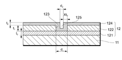
(1)微細孔形成工程
図1に示すように、ガラス基板11上に下地絶縁膜121としての酸化シリコン膜を形成する。膜厚t0はたとえば200nm程度である。次に前記下地絶縁膜121上に第一絶縁膜122として酸化シリコン膜を膜厚t1で形成する。次に前記第一絶縁膜122に直径d1の孔123を形成する。この形成手法としては、マスクを用いて前記第一絶縁膜122用上に塗布したフォトレジスト膜を露光、現像して、前記孔123の形成位置を露出させる開口部を有するフォトレジスト膜(図示せず)を第一絶縁膜122上に形成し、このフォトレジスト膜をエッチングマスクとして用いて反応性イオンエッチングを行い、その後、前記フォトレジスト膜を除去することによって形成することができる。次に前記孔123を含む前記第一絶縁膜122上に、第二絶縁膜124としての酸化シリコン膜を形成する。この第二絶縁膜124の平均膜厚はt2であるが、±y%の膜厚分布を有している。また第二絶縁膜124の堆積時の、前記第一絶縁膜122上部の平均膜厚t2に対する、前記孔123側面に堆積する膜厚の比をxとする。
(1) Micropore forming step As shown in FIG. 1, a silicon oxide film as a base
これら下地絶縁膜121、第一絶縁膜122、第二絶縁膜124はいずれも例えばTEOS(Tetra Ethyl Ortho Silicate)やシラン(SiH4)ガスを原料として用いたPECVD法により形成可能である。またその場合、前記xの値は一般に1以下の値となる。
These base
このように前記第一絶縁膜122に形成した孔123に対して第二絶縁膜124を堆積することによって、より径の小さい本発明の凹部としての微細孔125が形成され、その直径d2は、d2=d1―2*xt2で表される。実際には第二絶縁膜124の膜厚分布を考慮すると、直径d2は基板11面内においてd1―2*(1+y/100)*xt2 〜 d1―2*(1―y/100)*xt2の範囲のばらつきをもつ。
By depositing the second
後に述べる微細孔125からシリコン結晶粒を成長させる工程において、微細孔125の直径d2は20nmから150nmの範囲内にあることが望ましい。理由は先に述べた通りである。よって、
条件1:d1―2*(1+y/100)*xt2 ≧ 20nm、
条件2:d1―2*(1―y/100)*xt2 ≦ 150nm
を満たすように微細孔125を形成することで、後に述べる微細孔125からシリコン結晶粒を安定して成長させることが可能となる。
In the step of growing silicon crystal grains from the
Condition 1: d 1 −2 * (1 + y / 100) * xt 2 ≧ 20 nm
Condition 2: d 1 −2 * (1-y / 100) * xt 2 ≦ 150 nm
By forming the
そこで許容される最も広い条件として、条件1=20nm、条件2=150nmとして計算すると、
条件3:xt2=3250/ynm
を得る。
Therefore, as the broadest allowable condition, if calculation is performed with
Condition 3: xt 2 = 3250 / ynm
Get.
ここで、前記第一絶縁膜122に形成する孔の直径d1の適切な値を求めるため、前記微細孔125の直径d2を20nm〜150nmの中心値としてd2=85nmとすると、
条件4:d1=2*xt2+d2=2*3250/y+85nm=6500/y+85nm
を得る。よって、
条件5:d1≦6500/y+85nm
を満たすようにd1を設計することによって、安定して後述のシリコン結晶粒の形成が実現できる。
Here, in order to obtain an appropriate value of the diameter d 1 of the hole formed in the first insulating
Condition 4: d 1 = 2 * xt 2 + d 2 = 2 * 3250 / y + 85 nm = 6500 / y + 85 nm
Get. Therefore,
Condition 5: d 1 ≦ 6500 / y + 85 nm
By designing d 1 so as to satisfy the above, formation of silicon crystal grains described later can be realized stably.
特に一般的なPECVD法による絶縁膜形成では、膜厚均一性yは8%程度以下で堆積可能であることから、条件5より、d1は897.5nm以下で設計および形成することによって、安定したシリコン結晶粒の形成が実現できる。 In particular, in the formation of an insulating film by a general PECVD method, the film thickness uniformity y can be deposited at about 8% or less. Therefore, from condition 5, it is stable by designing and forming d 1 at 897.5 nm or less. The formation of silicon crystal grains can be realized.
一方、ガラス基板上に堆積する酸化シリコン膜の膜厚が1.5μm程度以上の場合、酸化シリコン膜の内部応力によってクラックや剥離が発生する場合が多くある。よってこの微細孔形成工程において堆積する全絶縁膜の厚さ:t0+t1+t2≦1500nmとすることが望ましい。 On the other hand, when the film thickness of the silicon oxide film deposited on the glass substrate is about 1.5 μm or more, cracks and peeling often occur due to internal stress of the silicon oxide film. Therefore, it is desirable that the thickness of all insulating films deposited in this microhole forming step: t 0 + t 1 + t 2 ≦ 1500 nm.
ガラス基板11を用いた場合、ガラス基板11からの不純物汚染を避けるために下地絶縁膜121の膜厚t0は100nm以上、望ましくは200nm程度が必要である。また第一絶縁膜122の膜厚t1は、第二絶縁膜124堆積後に形成される微細孔125の深さに関係し、これまでの発明者の実験結果から550nm程度以上が望ましい事がわかっている。よって、t2≦750nmとなる。
When the
これを上記条件4に適用入すると、
条件6:d1≦1500x+85nm
となる。
Applying this to condition 4 above,
Condition 6: d 1 ≦ 1500 × + 85 nm
It becomes.
よって、条件5と共に、条件6を満たす第一絶縁膜122に形成する孔123の直径d1を設計・形成することで、後述の結晶粒形成工程では、より安定したシリコン結晶粒の形成が実現できる。
Therefore, by designing and forming the diameter d 1 of the
一般にxは0.5〜1の値をとることから、条件6より、d1は835〜1585nm以下の大きさにすることが望ましいことがわかる。実際のPECVD法による酸化シリコン膜の成膜では、xは0.5〜0.6程度の値であることから、d1は835〜985nm以下に設計、形成することが望ましい。更に製造プロセス中のxの変動の影響を低減するためには、d1≦835nmで設計、形成することが更に望ましい。 Since x generally takes a value of 0.5 to 1, it can be seen from condition 6 that d 1 is preferably 835 to 1585 nm or less. In the actual film formation of a silicon oxide film by PECVD, x is a value of about 0.5 to 0.6, and therefore d 1 is preferably designed and formed to be 835 to 985 nm or less. Furthermore, in order to reduce the influence of fluctuation of x during the manufacturing process, it is further desirable to design and form with d 1 ≦ 835 nm.
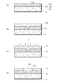
(2)結晶粒形成過程
図2は、シリコン膜13を形成する工程について説明する断面図である。
(2) Crystal Grain Formation Process FIG. 2 is a cross-sectional view illustrating a process for forming the
図2(a)は上記した工程によって製造された微細孔125である。以下、下地絶縁膜121、第一絶縁膜122、及び第二絶縁膜124を総称して、絶縁膜12を記載する。
FIG. 2A shows the
図2(b)に示すように、LPCVD法やPECVD法などの製膜法によって、前記第二絶縁膜124である酸化シリコン膜上および前記微細孔125内に、半導体膜として用いる非晶質シリコン膜130を形成する。この非晶質シリコン膜130は、50〜300nm程度の膜厚に形成することが好適である。また、非晶質シリコン膜130に代えて、多結晶シリコン膜を形成してもよい。なお、これらシリコン膜13をLPCVD法やPECVD法により形成した場合には、形成されるシリコン膜13中の水素含有量が比較的に多くなる場合がある。このような場合には、後述するレーザ照射時にシリコン膜のアブレーションが生じないようにするために、当該シリコン膜13の水素含有量を低くする(好適には1%以下)ための熱処理を行うとよい。
As shown in FIG. 2B, amorphous silicon used as a semiconductor film on the silicon oxide film as the second
次に、図2(c)に示すように、前記シリコン膜13に対してレーザ照射Lを行う。このレーザ照射Lは、例えば、波長308nm、パルス幅20〜30nsのXeClパルスエキシマレーザ、またはパルス幅200ns程度のXeClエキシマレーザを用いて、エネルギー密度が0.4〜2.0J/cm2程度となるように行うことが好適である。このような条件でレーザ照射を行うことにより、照射したレーザは、そのほとんどがシリコン膜13の表面付近で吸収される。これは、XeClパルスエキシマレーザの波長(308nm)における非晶質シリコンの吸収係数が0.139nm-1と比較的に大きいためである。
Next, as shown in FIG. 2C, laser irradiation L is performed on the
レーザ照射の条件を適宜に選択することにより、シリコン膜13を、微細孔125内の底部には非溶融状態の部分が残り、それ以外の部分については略完全溶融状態となるようにする。これによりレーザ照射後のシリコンの結晶成長は微細孔125の底部近傍で先に始まり、シリコン膜13の表面付近、すなわち略完全溶融状態の部分へ進行する。レーザ照射のエネルギー密度がこれよりやや強く、微細孔125内の底部に非溶融状態の部分が残らない場合においても、略完全溶融状態であるシリコン膜13の表面付近と微細孔125の底部との間には温度差が生じ、やはりレーザ照射後のシリコンの結晶成長は微細孔125の底部近傍で先に始まり、先と同様にシリコン膜13の表面付近、すなわち略完全溶融状態の部分へ進行し得る。
By appropriately selecting the laser irradiation conditions, the
シリコン結晶成長の初期段階では、微細孔125の底部においていくつかの結晶粒が発生し得る。このとき、微細孔125の断面寸法(本実施形態では、円の直径)を1個の結晶粒と同程度か少し小さい程度にしておくことにより、微細孔125の上部(開口部)には1個の結晶粒のみが到達するようになる。具体的には直径20nm〜150nm程度が適当である。これによりシリコン膜の略完全溶融状態の部分では、微細孔125の上部に到達した1個の結晶粒を核として結晶成長が進行するようになり、図2(d)に示すように、微細孔125を略中心とした大粒径のシリコン結晶粒131を規則的に配列してなるシリコン膜を形成可能となる。このシリコン結晶粒は、Σ3やΣ9やΣ27といった規則粒界(対応粒界)を含み得るが、不規則粒界を含まない略単結晶粒である。一般に不規則粒界は多くのシリコン不対電子を含むため、そこに形成する薄膜トランジスタの特性の低下や特性のばらつきの大きな要因となるが、本手法によって形成されるシリコン結晶粒131にはそれを含まないため、結晶粒内に薄膜トランジスタを形成することで、優れた特性を有する薄膜トランジスタが実現可能となる。しかしここで、前記微細孔125の直径が150nm程度以上の大きい直径を有する微細孔である場合は、微細孔125底部で発生した複数の結晶粒が微細孔上部まで成長して到達し、その結果、前記微細孔125を略中心として形成されるシリコン結晶粒には、不規則粒界を含むことになる。
In the initial stage of silicon crystal growth, several crystal grains may be generated at the bottom of the
なお、上述したレーザ照射による結晶化の際に、併せてガラス基板11を加熱することも好ましい。例えば、ガラス基板11を載置するステージによって当該ガラス基板11の温度が200℃〜400℃程度となるように加熱処理を行うとよい。このように、レーザ照射と基板加熱とを併用することにより、各シリコン結晶粒131の結晶粒径を更に大粒径化することが可能となる。基板加熱を併用することにより、当該加熱を行わない場合に比較してシリコン結晶粒131の粒径を概ね1.5倍〜2倍程度にすることができる。更には、基板加熱の併用によって結晶化の進行が緩やかになるため、シリコン結晶粒131の結晶性がより向上するという利点もある。
Note that it is also preferable to heat the
(3)薄膜トランジスタ形成工程
次に、上述したシリコン膜を用いて形成される薄膜トランジスタの構造について説明する。現状では、微細孔125を起点とした結晶化を行うことにより得られるシリコン結晶粒131の結晶粒径は6μm程度の大きさである。
(3) Thin Film Transistor Formation Step Next, the structure of the thin film transistor formed using the above-described silicon film will be described. At present, the crystal grain size of the
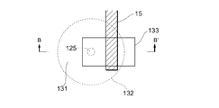
図3の平面図に示した薄膜トランジスタを形成する工程について説明する。図4は、薄膜トランジスタを形成する工程を説明する説明図であり、図3に示すB−B’方向の断面図を示している。 A process of forming the thin film transistor shown in the plan view of FIG. 3 will be described. FIG. 4 is an explanatory diagram for explaining a process of forming a thin film transistor, and shows a cross-sectional view in the B-B ′ direction shown in FIG. 3.
図4(a)に示すように、シリコン結晶粒131をパターニングし、薄膜トランジスタの形成に不要となる部分を除去して整形し半導体膜133とする。このとき、半導体膜133のチャネル形成領域135となる部分には、微細孔125及びその近傍を含まないようにする。これは微細孔125及びその周辺は結晶性の乱れが多いためである。
As shown in FIG. 4A, the
次に、図4(b)に示すように、第二絶縁膜124である酸化シリコン膜およびパターニングされた半導体膜133の上面に、電子サイクロトロン共鳴PECVD法(ECR−PECVD法)または平行平板型のPECVD法等によって酸化シリコン膜を形成する。この酸化シリコン膜は、薄膜トランジスタのゲート絶縁膜14として機能し、膜厚は10nm〜150nm程度が好ましい。
Next, as shown in FIG. 4B, an electron cyclotron resonance PECVD method (ECR-PECVD method) or a parallel plate type is formed on the upper surface of the silicon oxide film which is the second
次に、図4(c)に示すように、スパッタリング法などの製膜法によってタンタル、アルミニウム等の金属薄膜を形成した後に、パターニングを行うことによって、ゲート電極15及びゲート配線膜を形成する。そして、このゲート電極15をマスクとしてドナーまたはアクセプタとなる不純物元素を打ち込む、いわゆる自己整合イオン打ち込みを行うことにより、シリコン膜にソース領域及びドレイン領域134並びにチャネル形成領域135を形成する。例えば、本実施形態では、不純物元素としてリン(P)を打ち込み、その後、XeClエキシマレーザを200mJ/cm2〜400mJ/cm2程度のエネルギー密度に調整して照射して不純物元素を活性化することによって、N型の薄膜トランジスタを形成する。なお、レーザ照射の代わりに、250℃〜450℃程度の温度で熱処理を行うことにより、不純物元素の活性化を行ってもよい。
Next, as shown in FIG. 4C, after forming a metal thin film such as tantalum or aluminum by a film forming method such as a sputtering method, the
次に、図4(d)に示すように、ゲート絶縁膜14である酸化シリコン膜およびゲート電極15の上面に、PECVD法などの製膜法によって、500nm程度の膜厚の酸化シリコン膜を形成する。この酸化シリコン膜は層間絶縁膜16として機能する。次に、この層間絶縁膜16とゲート絶縁膜14を貫通してソース領域及びドレイン領域134のそれぞれに至るコンタクトホール161、162を形成し、これらのコンタクトホール内に、スパッタリング法などの製膜法によってアルミニウム、タングステン等の金属を埋め込み、パターニングすることによって、ソース電極181及びドレイン電極182を形成する。以上に説明した製造方法によって、本実施形態の薄膜トランジスタが形成される。
Next, as shown in FIG. 4D, a silicon oxide film having a thickness of about 500 nm is formed on the upper surface of the silicon oxide film as the
次に、本発明に係る薄膜トランジスタの適用例について説明する。本発明に係る薄膜トランジスタは、液晶表示装置のスイッチング素子として、あるいは有機EL表示装置の駆動素子として利用することができる。 Next, application examples of the thin film transistor according to the present invention will be described. The thin film transistor according to the present invention can be used as a switching element of a liquid crystal display device or as a drive element of an organic EL display device.
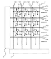
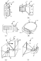
図5は、本実施形態の電気光学装置の一例である表示装置1の接続状態を示す図である。図5に示すように、表示装置1は、表示領域内に画素領域Gを配置して構成される。画素領域Gは有機EL発光素子OLEDを駆動する薄膜トランジスタT1〜T4を使用している。薄膜トランジスタT1〜T4は上述した実施形態の製造方法によって製造されるものが使用される。ドライバ領域2からは、発光制御線Vgpおよび書き込み制御線Vselが各画素領域Gに供給されている。ドライバ領域2からは、電流線Idataおよび電源線Vddが各画素領域Gに供給されている。書き込み制御線Vselと定電流線Idataを制御することにより、各画素領域Gに対する電流プログラムが行われ、発光制御線Vgpを制御することにより発光が制御される。また、本実施形態の薄膜トランジスタは、ドライバ領域2及び3についても本発明のトランジスタが使用可能であり、特にドライバ領域2に含まれる発光制御線Vgpおよび書き込み制御線Vselを選択するバッファー回路など大電流が必要とされる用途に有用である。
FIG. 5 is a diagram illustrating a connection state of the
図6は、表示装置1を適用可能な電子機器の例を示す図である。上述した表示装置1は、種々の電子機器に適用可能である。
FIG. 6 is a diagram illustrating an example of an electronic device to which the
図6(a)は携帯電話への適用例であり、当該携帯電話20は、アンテナ部21、音声出力部22、音声入力部23、操作部24、および本発明の表示装置1を備えている。このように本発明の表示装置は表示部として利用可能である。
FIG. 6A shows an application example to a cellular phone, and the
図6(b)はビデオカメラへの適用例であり、当該ビデオカメラ30は、受像部31、操作部32、音声入力部33、および本発明の表示装置1を備えている。このように本発明の表示装置は、ファインダや表示部として利用可能である。
FIG. 6B shows an application example to a video camera. The
図6(c)は携帯型パーソナルコンピュータ(いわゆるPDA)への適用例であり、当該コンピュータ40は、カメラ部41、操作部42、および本発明の表示装置1を備えている。このように本発明の表示装置は、表示部として利用可能である。
FIG. 6C shows an application example to a portable personal computer (so-called PDA). The computer 40 includes a camera unit 41, an operation unit 42, and the
図6(d)はヘッドマウントディスプレイへの適用例であり、当該ヘッドマウントディスプレイ50は、バンド51、光学系収納部52および本発明の表示装置1を備えている。このように本発明の表示パネルは画像表示源として利用可能である。
FIG. 6D shows an application example to a head-mounted display, and the head-mounted
図6(e)はリア型プロジェクターへの適用例であり、当該プロジェクター60は、筐体61に、光源62、合成光学系63、ミラー64、65、スクリーン66、および本発明の表示装置1を備えている。このように本発明の表示装置は画像表示源として利用可能である。
FIG. 6E shows an application example to a rear projector. The
図6(f)はフロント型プロジェクターへの適用例であり、当該プロジェクター70は、筐体72に光学系71および本発明の表示装置1を備え、画像をスクリーン73に表示可能になっている。このように本発明の表示装置は画像表示源として利用可能である。
FIG. 6F shows an application example to a front-type projector. The
本発明のトランジスタを使用した表示装置1は、上述した例に限らずアクティブ型あるいはパッシブマトリクス型の、液晶表示装置及び有機EL表示装置を適用可能なあらゆる電子機器に適用可能である。例えば、この他に、表示機能付きファックス装置、デジタルカメラのファインダ、携帯型TV、電子手帳、電光掲示盤、宣伝公告用ディスプレイなどにも活用することができる。
The
なお、上述した実施形態にかかる半導体装置の製造方法と素子転写技術とを組み合わせることも可能である。具体的には、上述した実施形態にかかる方法を適用して、転写元となる第1基板上に半導体装置を形成した後に、当該半導体装置を転写先となる第2基板上に転写(移動)する。これにより、第1基板については、半導体膜の成膜やその後の素子形成に都合のよい条件(形状、大きさ、物理的特性等)を備えた基板を用いることができるので、当該第1基板上に微細かつ高性能な半導体素子を形成することが可能となる。また、第2基板については、素子形成プロセス上の制約を受けることがなく、大面積化が可能となると共に、合成樹脂やソーダガラス等からなる安価な基板や可撓性を有するプラスチックフィルム等、幅広い選択肢から所望のものを用いることが可能となる。したがって、微細かつ高性能な薄膜半導体素子を大面積の基板に容易に(低コストに)形成することが可能となる。 It is possible to combine the semiconductor device manufacturing method and the element transfer technique according to the above-described embodiment. Specifically, after applying the method according to the above-described embodiment to form a semiconductor device on the first substrate serving as the transfer source, the semiconductor device is transferred (moved) onto the second substrate serving as the transfer destination. To do. Thereby, as the first substrate, a substrate having conditions (shape, size, physical characteristics, etc.) convenient for the formation of the semiconductor film and the subsequent element formation can be used. A fine and high-performance semiconductor element can be formed thereon. In addition, the second substrate is not subject to restrictions on the element formation process, and can be increased in area, and an inexpensive substrate made of synthetic resin, soda glass, or a flexible plastic film, It is possible to use a desired one from a wide range of options. Therefore, a fine and high-performance thin film semiconductor element can be easily (low cost) formed on a large-area substrate.
11…ガラス基板、 12(121、122、124)、14、16…酸化シリコン膜、 123…孔、 125…微細孔(凹部)、 13…シリコン膜、 131…シリコン結晶粒、 132…結晶粒界、 133…半導体膜(トランジスタ領域)、 15…ゲート電極、 134…ソース領域及びドレイン領域、 135…チャネル形成領域、 1…表示装置
DESCRIPTION OF
Claims (6)
前記基板上に下地絶縁膜を形成する工程と、
前記下地絶縁膜上に第一絶縁膜を形成する工程と、
前記第一絶縁膜に直径d1の孔を形成する工程と、
前記凹部を含む前記第一絶縁膜上に第二絶縁膜を形成する工程とを含み、
前記第二絶縁膜の形成工程での基板面内での膜厚分布が±y%である場合に、前記孔の直径d1が、
d1≦6500/y+85nm
という関係を満たすことを特徴とする半導体装置の製造方法。 A method of manufacturing a semiconductor device, wherein a thin film transistor is formed using a semiconductor film on an insulating substrate having at least one surface,
Forming a base insulating film on the substrate;
Forming a first insulating film on the base insulating film;
Forming a hole with a diameter d 1 in the first insulating film;
Forming a second insulating film on the first insulating film including the recess,
When the film thickness distribution in the substrate plane in the step of forming the second insulating film is ± y%, the diameter d 1 of the hole is
d 1 ≦ 6500 / y + 85 nm
A manufacturing method of a semiconductor device characterized by satisfying the relationship:
d1≦897.5nm
という関係を満たす、請求項1に記載の半導体装置の製造方法。 Furthermore, the diameter d 1 of the hole is
d 1 ≦ 897.5 nm
The method for manufacturing a semiconductor device according to claim 1, satisfying the relationship:
d1≦1500x+85nm
という関係を満たす、請求項1または2に記載の半導体装置の製造方法。 In the step of forming the second insulating film, when the ratio of the thickness of the second insulating film deposited on the sidewall of the hole to the thickness of the second insulating film on the first insulating film is x, The diameter d 1 of the hole is
d 1 ≦ 1500x + 85nm
The method for manufacturing a semiconductor device according to claim 1, wherein the method satisfies the relationship:
d1≦835nm
という関係を満たす、請求項3に記載の半導体装置の製造方法。 Furthermore, the diameter d 1 of the hole is
d 1 ≦ 835 nm
The method for manufacturing a semiconductor device according to claim 3, satisfying the relationship:
前記半導体膜は、前記基板上に設けられた起点部を起点として形成された略単結晶粒を含んでおり、
前記起点部は基板上に形成された凹部であり、
前記凹部は、第一絶縁膜に形成された直径897.5nm以下の孔に第二絶縁膜を堆積したものである、半導体装置。 A semiconductor device comprising a thin film transistor formed using a semiconductor film having at least one surface formed on an insulating substrate,
The semiconductor film includes substantially single crystal grains formed with a starting point provided on the substrate as a starting point,
The starting point is a recess formed on the substrate,
The recess is a semiconductor device in which a second insulating film is deposited in a hole having a diameter of 897.5 nm or less formed in the first insulating film.
Priority Applications (5)
| Application Number | Priority Date | Filing Date | Title |
|---|---|---|---|
| JP2004109099A JP2005294630A (en) | 2004-04-01 | 2004-04-01 | Semiconductor device, electro-optical device, integrated circuit, and electronic equipment |
| KR1020050019437A KR100726855B1 (en) | 2004-04-01 | 2005-03-09 | Semiconductor devices, electro-optical devices, integrated circuits and electronics |
| TW094107728A TWI258875B (en) | 2004-04-01 | 2005-03-14 | Manufacturing method of semiconductor device and semiconductor device |
| CNA2005100547993A CN1677617A (en) | 2004-04-01 | 2005-03-16 | Semiconductor device, electro-optic device, integrated circuit, and electronic apparatus |
| US11/095,553 US7148095B2 (en) | 2004-04-01 | 2005-04-01 | Semiconductor device, electro-optic device, integrated circuit, and electronic apparatus |
Applications Claiming Priority (1)
| Application Number | Priority Date | Filing Date | Title |
|---|---|---|---|
| JP2004109099A JP2005294630A (en) | 2004-04-01 | 2004-04-01 | Semiconductor device, electro-optical device, integrated circuit, and electronic equipment |
Publications (1)
| Publication Number | Publication Date |
|---|---|
| JP2005294630A true JP2005294630A (en) | 2005-10-20 |
Family
ID=35050037
Family Applications (1)
| Application Number | Title | Priority Date | Filing Date |
|---|---|---|---|
| JP2004109099A Pending JP2005294630A (en) | 2004-04-01 | 2004-04-01 | Semiconductor device, electro-optical device, integrated circuit, and electronic equipment |
Country Status (5)
| Country | Link |
|---|---|
| US (1) | US7148095B2 (en) |
| JP (1) | JP2005294630A (en) |
| KR (1) | KR100726855B1 (en) |
| CN (1) | CN1677617A (en) |
| TW (1) | TWI258875B (en) |
Families Citing this family (3)
| Publication number | Priority date | Publication date | Assignee | Title |
|---|---|---|---|---|
| JP2003282438A (en) * | 2002-03-27 | 2003-10-03 | Seiko Epson Corp | Semiconductor device manufacturing method, semiconductor device, electro-optical device, and electronic equipment |
| EP2239084A1 (en) * | 2009-04-07 | 2010-10-13 | Excico France | Method of and apparatus for irradiating a semiconductor material surface by laser energy |
| CN106098864A (en) * | 2016-06-28 | 2016-11-09 | 山东浪潮华光光电子股份有限公司 | A kind of pasting method in LED gallium arsenide substrate reduction process |
Family Cites Families (6)
| Publication number | Priority date | Publication date | Assignee | Title |
|---|---|---|---|---|
| JP3476320B2 (en) * | 1996-02-23 | 2003-12-10 | 株式会社半導体エネルギー研究所 | Semiconductor thin film and method for manufacturing the same, semiconductor device and method for manufacturing the same |
| EP1420437A4 (en) * | 2001-07-25 | 2006-02-08 | Seiko Epson Corp | PROCESS FOR PRODUCING SEMICONDUCTOR FINE FILM, PROCESS FOR PRODUCING SEMICONDUCTOR DEVICE, SEMICONDUCTOR DEVICE, INTEGRATED CIRCUIT, ELECTROOPTIC DEVICE, AND ELECTRONIC APPARATUS |
| KR20030034526A (en) * | 2001-10-25 | 2003-05-09 | 플러스원테크 주식회사 | Realization method for fingerprint authentication process and the system on IP network |
| US6933527B2 (en) * | 2001-12-28 | 2005-08-23 | Semiconductor Energy Laboratory Co., Ltd. | Semiconductor device and semiconductor device production system |
| US7749818B2 (en) * | 2002-01-28 | 2010-07-06 | Semiconductor Energy Laboratory Co., Ltd. | Semiconductor device and method of manufacturing the same |
| JP2003282438A (en) * | 2002-03-27 | 2003-10-03 | Seiko Epson Corp | Semiconductor device manufacturing method, semiconductor device, electro-optical device, and electronic equipment |
-
2004
- 2004-04-01 JP JP2004109099A patent/JP2005294630A/en active Pending
-
2005
- 2005-03-09 KR KR1020050019437A patent/KR100726855B1/en not_active Expired - Fee Related
- 2005-03-14 TW TW094107728A patent/TWI258875B/en not_active IP Right Cessation
- 2005-03-16 CN CNA2005100547993A patent/CN1677617A/en active Pending
- 2005-04-01 US US11/095,553 patent/US7148095B2/en not_active Expired - Fee Related
Also Published As
| Publication number | Publication date |
|---|---|
| TWI258875B (en) | 2006-07-21 |
| US7148095B2 (en) | 2006-12-12 |
| KR20060043552A (en) | 2006-05-15 |
| KR100726855B1 (en) | 2007-06-12 |
| TW200534514A (en) | 2005-10-16 |
| US20050233594A1 (en) | 2005-10-20 |
| CN1677617A (en) | 2005-10-05 |
Similar Documents
| Publication | Publication Date | Title |
|---|---|---|
| JP4900756B2 (en) | Semiconductor device manufacturing method, electro-optical device, integrated circuit, and electronic apparatus | |
| JPWO2003010804A1 (en) | Semiconductor thin film manufacturing method, semiconductor device manufacturing method, semiconductor device, integrated circuit, electro-optical device, and electronic equipment | |
| JP2003197526A (en) | Semiconductor device manufacturing method, semiconductor device, display device, and electronic apparatus | |
| JP4019377B2 (en) | Semiconductor device manufacturing method and semiconductor device | |
| KR100726855B1 (en) | Semiconductor devices, electro-optical devices, integrated circuits and electronics | |
| JP2008060532A (en) | Semiconductor device | |
| JP4247661B2 (en) | Semiconductor thin film manufacturing method and semiconductor device manufacturing method | |
| JP2005340466A (en) | Semiconductor device, electro-optical device, integrated circuit, and electronic equipment | |
| JP2005327966A (en) | Semiconductor device, electro-optical device, integrated circuit, and electronic equipment | |
| JP4560708B2 (en) | Semiconductor device and manufacturing method thereof | |
| JP2007189106A (en) | Semiconductor device manufacturing method, semiconductor device, integrated circuit, electro-optical device, electronic apparatus | |
| JP2006049647A (en) | Active matrix substrate, electro-optical device, electronic device, and manufacturing method of active matrix substrate | |
| JP2004134581A (en) | Semiconductor device manufacturing method, semiconductor device, electro-optical device, and electronic apparatus | |
| JP2006086436A (en) | Semiconductor device manufacturing method, electro-optical device, and electronic device | |
| JP2008047750A (en) | Manufacturing method of semiconductor device | |
| JP2004228160A (en) | Semiconductor device manufacturing method, electro-optical device, and electronic apparatus | |
| JP2007194316A (en) | Manufacturing method of semiconductor device | |
| JP4333115B2 (en) | Semiconductor device manufacturing method, semiconductor device, electro-optical device, and electronic apparatus | |
| JP2005353939A (en) | Semiconductor device manufacturing method, electro-optical device, integrated circuit, and electronic apparatus | |
| JP2004172479A (en) | Semiconductor thin film manufacturing method, semiconductor device manufacturing method, semiconductor device, integrated circuit, electro-optical device, and electronic equipment | |
| JP2004186206A (en) | Semiconductor device manufacturing method, semiconductor device, electro-optical device, and electronic equipment | |
| JP2005026330A (en) | Manufacturing method of semiconductor device, semiconductor device, electro-optical device, and electronic apparatus | |
| JP2007189105A (en) | Semiconductor device manufacturing method, semiconductor device, integrated circuit, electro-optical device, electronic apparatus | |
| JP2004186207A (en) | Semiconductor device manufacturing method, semiconductor device, electro-optical device, and electronic equipment | |
| JP2004235570A (en) | Semiconductor device manufacturing method, semiconductor device, electro-optical device, and electronic apparatus |
Legal Events
| Date | Code | Title | Description |
|---|---|---|---|
| A977 | Report on retrieval |
Free format text: JAPANESE INTERMEDIATE CODE: A971007 Effective date: 20070611 |
|
| A131 | Notification of reasons for refusal |
Free format text: JAPANESE INTERMEDIATE CODE: A131 Effective date: 20070614 |
|
| A521 | Request for written amendment filed |
Free format text: JAPANESE INTERMEDIATE CODE: A523 Effective date: 20070810 |
|
| A02 | Decision of refusal |
Free format text: JAPANESE INTERMEDIATE CODE: A02 Effective date: 20070830 |