EP1419514B1 - Split double gap buncher and method for ion bunching in an ion implantation system - Google Patents
Split double gap buncher and method for ion bunching in an ion implantation system Download PDFInfo
- Publication number
- EP1419514B1 EP1419514B1 EP02753518A EP02753518A EP1419514B1 EP 1419514 B1 EP1419514 B1 EP 1419514B1 EP 02753518 A EP02753518 A EP 02753518A EP 02753518 A EP02753518 A EP 02753518A EP 1419514 B1 EP1419514 B1 EP 1419514B1
- Authority
- EP
- European Patent Office
- Prior art keywords
- ion
- buncher
- ions
- electrode
- energy
- Prior art date
- Legal status (The legal status is an assumption and is not a legal conclusion. Google has not performed a legal analysis and makes no representation as to the accuracy of the status listed.)
- Expired - Lifetime
Links
Images


Classifications
-
- H—ELECTRICITY
- H05—ELECTRIC TECHNIQUES NOT OTHERWISE PROVIDED FOR
- H05H—PLASMA TECHNIQUE; PRODUCTION OF ACCELERATED ELECTRICALLY-CHARGED PARTICLES OR OF NEUTRONS; PRODUCTION OR ACCELERATION OF NEUTRAL MOLECULAR OR ATOMIC BEAMS
- H05H7/00—Details of devices of the types covered by groups H05H9/00, H05H11/00, H05H13/00
- H05H7/14—Vacuum chambers
- H05H7/18—Cavities; Resonators
-
- H—ELECTRICITY
- H01—ELECTRIC ELEMENTS
- H01J—ELECTRIC DISCHARGE TUBES OR DISCHARGE LAMPS
- H01J37/00—Discharge tubes with provision for introducing objects or material to be exposed to the discharge, e.g. for the purpose of examination or processing thereof
- H01J37/30—Electron-beam or ion-beam tubes for localised treatment of objects
- H01J37/317—Electron-beam or ion-beam tubes for localised treatment of objects for changing properties of the objects or for applying thin layers thereon, e.g. for ion implantation
- H01J37/3171—Electron-beam or ion-beam tubes for localised treatment of objects for changing properties of the objects or for applying thin layers thereon, e.g. for ion implantation for ion implantation
-
- H—ELECTRICITY
- H01—ELECTRIC ELEMENTS
- H01J—ELECTRIC DISCHARGE TUBES OR DISCHARGE LAMPS
- H01J2237/00—Discharge tubes exposing object to beam, e.g. for analysis treatment, etching, imaging
- H01J2237/04—Means for controlling the discharge
- H01J2237/047—Changing particle velocity
- H01J2237/0473—Changing particle velocity accelerating
- H01J2237/04735—Changing particle velocity accelerating with electrostatic means
- H01J2237/04737—Changing particle velocity accelerating with electrostatic means radio-frequency quadrupole [RFQ]
-
- H—ELECTRICITY
- H01—ELECTRIC ELEMENTS
- H01J—ELECTRIC DISCHARGE TUBES OR DISCHARGE LAMPS
- H01J2237/00—Discharge tubes exposing object to beam, e.g. for analysis treatment, etching, imaging
- H01J2237/04—Means for controlling the discharge
- H01J2237/049—Focusing means
- H01J2237/0492—Lens systems
- H01J2237/04924—Lens systems electrostatic
Definitions
- the present invention relates generally to ion implantation systems, and more specifically to methods and apparatus for improved ion bunching in an ion implantation system.
- HE high energy
- Such HE ion implanters are used for deep implants into a substrate in creating, for example, retrograde wells. Implant energies of 1.5 MeV (million electron volts), are typical for such deep implants. Although lower energy may be used, such implanters typically perform implants at energies between at least 300 keV and 700 keV. Some HE ion implanters are capable of providing ion beams at energy levels up to 5 MeV.
- a typical high energy ion implanter 10 having a terminal 12, a beamline assembly 14, and an end station 16.
- the terminal 12 includes an ion source 20 powered by a high voltage power supply 22.
- the ion source 20 produces an ion beam 24 that is provided to the beamline assembly 14.
- the ion beam 24 is then directed toward a target wafer 30 in the end station 16.
- the ion beam 24 is conditioned by the beamline assembly 14 that comprises a mass analysis magnet 26 and a radio frequency (RF) linear accelerator (linac) 28.
- the linac 28 includes a series of accelerating modules 28a-28n, each of which further accelerates ions beyond the energies they achieve from prior modules.
- the accelerating modules maybe individually energized by a high RF voltage that is typically generated by a resonance method to keep the required average power reasonable.
- the mass analysis magnet 26 passes only ions of an appropriate charge-to-mass ratio to the linac 28.
- the linear accelerating modules 28a-28n in the high energy ion implanter 10 individually include an RF amplifier, a resonator, and an energizable electrode.
- the resonators for example, as described in U.S. Patent No. 4,667,111 operate at a frequency in the range of about 3-30 Mhz, with a voltage of about 0 to 150 kV, in order to accelerate ions of the beam 24 to energies over one million electron volts per charge state.
- conventional linear accelerators 28 achieve an ion acceleration efficiency that is less than 100%.
- conventional ion accelerators may deliver less than 20% of the ions from the mass analysis magnet 26 to the target wafer 30 in the end station 16.
- each ion accelerating stage 28a-28n is tuned or adjusted in order to provide appropriate acceleration to ions provided thereto which fall within a tolerance or acceptance range. Maintaining ions in an ion beam is facilitated where the ions are bunched or packetized prior to acceleration, whereby a larger percentage of ions are accelerated by each accelerating module or stage 28.
- the first or the first and second accelerating modules e.g. modules 28a, 28b
- this bunching provides limited ion transfer efficiency.
- typical linear accelerators 28 may achieve less than 20% transmission of ions.
- ions In ion implantation devices, it is desirable to impart ions onto a workpiece, such as a semiconductor product, in a controlled fashion. In conventional systems where approximately 80% of ions generated by an ion source therein may be lost (e.g. not provided to the workpiece), more time is needed to perform the desired implantation.
- EP 1 056 113 discloses an ion implanter with two three gap rf accelerator stages to boost the implant energy after mass selection.
- the electrodes of the accelerator stages have slit-shaped apertures that accommodate high beam current, when the accelerator is in drift mode.
- each stage of the accelerator produces accelerated ions having a relatively small energy spread, even though the acceptance range of the accelerator stage extends over a substantial phase angle of the applied rf voltage.
- the resulting accelerator is flexible, permitting a wide variation of output energies with good beam dynamics. Ion bunches from the first three gap stage are caused to have the correct flight time to reach the second stage for acceleration by adjusting the speed of the ions while maintaining the rf phase of the fields in the two stages locked to fixed values.
- US 4 284 923 discloses an ion beam buncher-debuncher of the type having a resonant structure supplied by a high frequency or hyperfrequency generator, said structure comprising a cylindrical wall closed by two lateral faces respectively traversed by a supply pipe and a discharge pipe for the beam, together with a sliding tube arranged between the said pipes and defining with the supply pipe a first gap and with the discharge pipe a second gap, the ion beam being introduced into the said structure by the supply pipe firstly undergoing in the first gap a first action on the part of the electrical field therein, then traversing the sliding pipe and finally undergoing in the second gap a second action on the part of the electrical field therein and leaving the structure by the discharge pipe, wherein the two gaps defined by the sliding tube and the supply and discharge pipes are extremely asymmetrical, one of the two gaps offering the ion beam a much weaker electrical field than that offered by the other gap, so that the action exerted on the ions in said gap by the electrical field is negligible compared with that
- the present invention is directed to a linear accelerator having an ion buncher associated therewith that achieves improved ion transport in an ion implantation system.
- the invention provides a dedicated buncher stage for ensuring that a greater percentage of the generated ions are provided in the region of acceleration for the accelerating stage of the ion implanter, than was heretofore possible.
- the buncher stage may be positioned upstream of a linear accelerator stage along a beam path in an ion implantation system in order to provide bunches or packets of ions to the accelerating stage of the accelerator.
- the invention provides for beam transmission of up to 60%, for example, of the available ions through the linear accelerator of an ion implantation system.
- the invention provides significant advantages over conventional ion implantation devices and methodologies in which in some cases less than 20% of available ions were properly accelerated.
- an ion buncher for grouping ions along a path between an entrance end and an accelerating module in an ion accelerator system, the buncher comprising: a first grounded electrode forming an entrance aperture for an ion beam with an elongated slit shaped transverse profile; a second grounded electrode, located along the ion beam path toward the accelerating module; and an energizable electrode located between the first and second grounded electrodes and defining gaps therebetween, and operatively associated with an energy source and adapted to create a modulating electric field in the gaps between the energizable electrode and the first and second grounded electrodes, respectively, to provide bunched ions to the accelerating module, wherein said first grounded electrode has an elongated slit aperture, said second grounded electrode has either a slit aperture or a circular aperture, and said energizable electrode has an elongated slit aperture, characterized in that said gaps have different lengths, and one of said gaps is adjustable.
- the modulating field in the buncher accelerates certain ions with respect to a reference ion, and decelerates others with respect thereto.
- the accelerated ions catch up to the reference ion and the decelerated ions slow down to allow the reference ion (e.g. as well as the accelerated ions) to catch up, thereby providing a net bunching effect.
- the asymmetry of the gaps facilitates the provision of a higher percentage of available ions to subsequent linear accelerator stages, thereby significantly improving the ion transfer efficiency of ion implantation systems.
- the asymmetrical double gap buncher may be included as a buncher stage within a linear accelerator system for an ion implanter in which the modulating field strength created by the buncher electrode may be significantly lower than that of the accelerating alternating electric field of the linear accelerator.
- the buncher electrode operates to modulate the DC ion beam (e.g., obtained from an upstream mass analysis magnet), and the drift region allows bunching to occur as a result of the modulation.
- a slit double gap buncher stage and a modulating electrode therefor which provide further advantages associated with ion implantation.
- the modulating electrode comprises an elongated slit aperture in an electrode base extending longitudinally through the base along the ion beam path.
- the slit may comprise an aspect ratio greater than one, for example, in which the slit height is greater than the slit width.
- the slit aperture allows reduced gap lengths in the buncher compared to circular electrode apertures, resulting in efficient modulation over a wider range of ion velocities.
- the slit double gap buncher may be located between matching quadrupole focusing devices and an entrance aperture in a linear accelerator. In this case, the matching quadrupoles may serve to form the bunched ion beam into a circular profile for injection into the first accelerating stage, as well as to provide a buncher drift region. This provides for reduction in length for an ion implantation device.
- a dedicated ion buncher stage is provided for bunching ions in an ion implantation system.
- the ion buncher stage may be employed in a linear accelerator upstream of an accelerating stage to provide ions thereto in bunches or packets, such that the loss of ions in the linear accelerator is reduced.
- the buncher stage may operate at lower energy levels than the subsequent accelerator stages, and may further provide a drift region to facilitate ion bunching.
- the invention further includes an asymmetrical double gap buncher stage, as well as a slit buncher stage for further improvement of ion implantation efficiency. Also described hereinafter are methods for accelerating ions in an ion implanter linear accelerator.
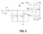
- a conventional resonator circuit 100 which includes an inductor coil L connected in parallel with a resistance R L and a capacitance C s .
- An energizable electrode 108 is connected to the inductor L.
- the electrode 108 is mounted between two grounded electrodes 112 and 114, and the energizable electrode 108 and the grounded electrodes 112 and 114 operate to accelerate the ion beam 110.
- the capacitance C s represents the capacitance of the energizable electrode 108
- the resistance R L represents the losses associated with the resonant circuit comprising the inductor L and the capacitance C s .
- the values for the capacitance C s and the inductor coil L are selected to form a low loss (high Q) resonant or "tank" circuit 100, wherein each accelerator module in a linear accelerator system of the type shown in Fig. 1 resonates at the same frequency.
- a radio frequency (RF) signal is connected from a matching network (not shown) at point 116 and is capacitively coupled to a high voltage end of the coil L via a capacitor C c .
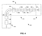
- a perspective view of a portion of a modular linear accelerator 228 is provided in Fig. 3 .
- a DC ion beam 224a is provided to the accelerator 228 (e.g., from an upstream mass analyzer magnet, not shown), along a beam path 226.
- the DC beam 224a may comprise, for example, an elongated slit profile that is passed through an entrance aperture 230 having a vertically elongated slit 232 along the path 226.
- the beam 224a is formed into a generally circular profile (not shown) via two sets of matching quadrupole devices 234 and corresponding grounded electrodes 236, wherein the grounded electrodes 236 each comprise a cylindrical aperture 238 located along the path 226.
- the linear accelerator 228 in the present example further comprises two or more accelerating modules or stages 228a, 228b, ...228n, where n is an integer, two of which ( e.g. , stages 228a and 228b) are illustrated in Fig. 3 .
- Each of the accelerator modules 228n further accelerates ions from the beam 224 beyond the energies they achieve from prior modules.
- the accelerating modules 228n may be individually energized by high RF voltages generated by a power supply and resonator (not shown). As the ion beam 224 travels through the various accelerating modules or stages 228n, some of the ions therein are accelerated, whereas others are not.
- the accelerating module 228a comprises a pair of grounded electrodes 246 located before and after an energizable electrode 248 along the path 226, where the energizable electrode 248 may be energized by an appropriate RF energy source and resonator (not shown) in order to achieve acceleration of ions within the beam 224a along the beam path 226.
- the grounded electrodes 246 are generally equally spaced from the energizable electrode 248 to provide first and second generally equal gaps 250a and 250b therebetween.
- the second accelerator module or stage 228b comprises a first grounded electrode 256 located along the path 226 upstream of a second energizable electrode 258.
- a quadrupole device 264 may be provided along the path 226 between the first and second accelerator stages 228a and 228b to provide for radial focusing of the beam 224 as it travels through successive accelerator stages 228.
- the accelerator 228 may comprise further accelerating stages or modules (not shown), whereby an ion beam 224b may be accelerated to an energy higher than that of the DC beam 224a provided to the accelerator 228.
- an aspect of the invention provides an ion implanter 310 comprising a terminal 312, a beamline assembly 314, and an end station 316.
- the terminal 312 includes an ion source 320 powered by a high voltage power supply 322.
- the ion source 320 produces an ion beam 324 that is provided to the beamline assembly 314.
- the ion beam 324 is then directed toward a target wafer 330 in the end station 316.
- the ion beam 324 is conditioned by the beamline assembly 314 that comprises a mass analysis magnet 326 and a radio frequency (RF) linear accelerator (linac) 328.
- RF radio frequency
- the linac 328 includes a buncher stage 340 and a series of accelerating stages or modules 328a-328n, each of which further accelerates ions beyond the energies they achieve from prior modules.
- the accelerating stages or modules may be individually energized by a high RF voltage that is typically generated by a resonance method to keep the required average power reasonable.
- the accelerating stages or modules 328a-328n in the high energy ion implanter 310 for example, individually include an RF amplifier, a resonator, and an accelerating electrode (not shown).
- the ion buncher stage 340 is located at the front of the linear accelerator between the mass analysis magnet 326 and the first accelerating stage 328a.
- the ion buncher stage 340 may comprise a buncher electrode located along the path 324, which is operatively associated with a buncher energy source (not shown) to create a modulating alternating electric field. This modulating field operates on the DC ion beam provided by the mass analysis magnet 326 in order to provide bunched ions to the accelerating stage 328a.
- the implanter 310 may further comprise controls (not shown), whereby the terminal 312, beamline assembly 314, and end station 316 may be operated to affect ion implantation in the workpiece 310 in a controlled fashion.
- controls not shown
- the modulating field in the buncher stage 340 as well as the accelerating fields in the linac 328 may be implemented through such controls.
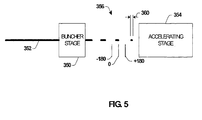
- a schematic illustration is provided of an exemplary buncher stage 350 operating on a DC ion beam 352 in order to group or "packetize" ions therefrom for provision to an ion accelerating stage 354.
- Buncher 350 may operate in similar fashion to the buncher 340 stage of Fig. 4
- the accelerating stage 354 may operate in similar fashion to the accelerating stage 328 of Fig. 4 .
- the buncher 350 receives the DC ion beam 352 having a uniform energy distribution and groups ions therefrom into bunches 356 of ions within a particular desired energy range, which may then be efficiently accelerated to a desired second energy (e.g. , or energy range) by the accelerator 354.
- a desired second energy e.g. , or energy range
- the invention contemplates a single modulating buncher electrode, which may be located between two grounded electrodes (e.g. , or grounded focusing devices, such as electrostatic quadrupoles).
- the buncher may comprise first and second grounded electrodes, wherein the first grounded electrode is spaced along a beam path from the buncher electrode toward an ion beam entrance end so as to define a first gap therebetween.
- the second grounded electrode may be spaced along the path from the buncher electrode toward the ion beam exit so as to define a second gap therebetween.
- one gap may be made larger than the other gap, for example, approximately ten times larger.
- one or both of the gaps may be mechanically or otherwise adjustable.
- an exemplary double gap buncher 500 is illustrated along with various components of an ion implantation linear accelerator 528.
- a DC ion beam (not shown) is provided to the accelerator 528 ( e.g. , from an upstream mass analyzer magnet, not shown), along a beam path 526.
- the DC beam may comprise, for example, an elongated slit profile that is passed through an entrance aperture 530 having a vertically elongated slit 532 along the path 526.
- the DC beam is formed into a generally circular profile via two sets of matching quadrupole devices 534 and corresponding grounded electrodes 536, wherein the grounded electrodes 536 each comprise a cylindrical aperture 538 located along the path 526.
- the linear accelerator 528 further comprises the asymmetrical gap buncher 500 as well as one or more accelerating modules or stages 528n, where n is an integer, one of which (528a) is illustrated in Fig. 6 .
- Each of the accelerating modules 528n further accelerates ions from the beam beyond the energies they achieve from prior modules.
- the buncher 500 comprises a pair of grounded electrodes 546a and 546b located before and after a modulating buncher electrode 548 along the path 526, where the modulating buncher electrode 548 may be energized by an appropriate RF energy source and resonator (not shown) in order to modulate ions within the beam along the beam path 526.
- the grounded electrodes 546a and 546b are spaced from the modulating electrode 548 to provide first and second gaps 550a and 550b, respectively, therebetween.
- One of the two gaps (e.g. , the first gap 550a) has a length such that the ion transit time through the gap is small compared to the RF period associated therewith. An ion passing through this gap experiences a maximum energy change slightly less than the product of its charge and the peak RF voltage applied to the energized buncher electrode 548.
- the other gap (e.g. , the second gap 550b) has a substantially greater length, so that the ion transit time through the gap is a large fraction of the RF period. An ion passing through this gap experiences a maximum energy change substantially less than the product of its charge and the peak RF voltage applied to the energized buncher electrode 548. Thus, most of the energy modulation of the ion beam occurs in the shorter of the two gaps.
- the bunching efficiency depends strongly on the ion transit time from the center of one gap to the center of the other gap. Efficiency is highest when the gap-to-gap transit time is one half of an RF period, as the second gap modulation enhances the first gap modulation. Efficiency is lowest when the gap-to-gap transit time is one RF period, as the second gap modulation tends to cancel the first gap modulation.
- the use of unequal length gaps greatly reduces the dependence of buncher efficiency on the gap-to-gap transit time, making efficiency nearly independent of ion species. It should be understood that wide variations in gap length may be employed and are contemplated as falling within the scope of the present invention.
- first gap 550a is less than the second gap 550b, it should be understood that the second gap may be made smaller than the first gap, in which case the functions thereof may switch.
- the gaps 550a, 550b may be adjusted in order to tune the buncher 500 to ion species.
- the power source energizing the modulating electrode 548 may be adjustable ( e.g. , with respect to frequency, phase, amplitude, etc.) in order to provide appropriate modulation according to one or more system performance parameters.
- the exemplary buncher 500 is adaptable for use with accelerators and ion implantation systems optimized for accelerating and implanting specific ion species, as well as those systems wherein the accelerator itself is adjustable.
- the accelerating module or stage 528a comprises a first grounded electrode 556 located along the path 526 upstream of an energizable electrode 558, as well as a second grounded electrode (not shown) downstream of the energizable electrode 558.
- the energizable electrode 558 may be energized by an appropriate power source and resonator (not shown) to affect acceleration of ions to a second energy level along the path 526 in a controlled fashion.
- a set of four focusing quadrupoles 564 may be provided along the path 526 between the buncher stage 500 of the accelerator system 528 and the first accelerator stage 528a in order to provide radial focusing of the beam as it travels through successive accelerator stages 528n.
- the accelerator system 528 may comprise further accelerator stages or modules 528n (not shown), whereby an accelerated ion beam may be generated at an energy level higher than that of the DC beam provided to the accelerator 528.
- the linear accelerator system 528 is illustrated schematically, wherein a transversely elongated DC ion beam 524a is provided to the entrance aperture 530 ( e.g. , having an elongated slit opening).
- the elongated profile of the beam 524a is shaped by matching quadrupoles 534 into a generally circular beam 524b, after which the beam 524b is provided to the exemplary buncher stage 500 of the accelerator system 528.
- the buncher stage 500 groups or bunches ions from the beam 524b into a bunched ion beam 524c As discussed above, the focusing quadrupoles 564 following the buncher stage 500 maintain this circular profile, and may further provide a drift region to facilitate bunching.
- the bunched beam 524c is then provided to the accelerating stages 528a-528n of the accelerator system 528, whereby an accelerated ion beam 524d is obtained, having an energy greater than that of the original DC beam 524a.
- a buncher which may operate directly on an ion beam (e.g. , beam 524a) having a transversely elongated longitudinal profile.
- an ion beam e.g. , beam 524a
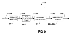
- a portion of another exemplary linear accelerator 628 is illustrated having an exemplary slit double gap buncher stage 600 of the accelerator system 628 positioned along a beam path 626 between an entrance aperture 630 having an elongated slit opening 632 therein, and subsequent matching quadrupoles 634 and associated grounded electrodes 636.
- One or more accelerating stages or modules 628a-628n of the accelerator system 628 are located downstream of the quadrupoles 634 along the path 626, one of which ( e.g. , 628a) is illustrated in Fig. 8 .
- the exemplary slit double gap buncher 600 comprises a single modulating buncher electrode 648, which may be located between the entrance aperture 630 and a grounded electrode 636 associated with the quadrupole devices 634, wherein the electrode 648 includes a transversely elongated slit aperture 604.
- the buncher electrode 648 is spaced from the entrance aperture 630 so as to define a first gap 650a therebetween.
- the grounded electrode 636 may be spaced along the path 626 from the buncher electrode 648 toward the accelerating stage 628a so as to define a second gap 650b therebetween.
- the second gap 650b may be made larger than the first gap 650a to obtain the advantages associated with asymmetrical gaps highlighted above, for instance, approximately at least ten times larger than the first gap 650a.
- the asymmetry of the gaps may further be selected to be a function of the ion transit time through the gap and the modulation frequency, which dictates the modulation voltage period.
- the slit aperture 604 of the modulating buncher electrode 648 allows the introduction of a ribbon shaped ion beam directly into the buncher 600 without requiring preliminary shaping (e.g. , via matching quadrupole devices) into a circular profile.
- the buncher stage 600 may be located immediately subsequent the entrance aperture 630 along the beam path 626. This provides for a reduction in the physical length of the accelerator system 628.
- the elongated-profile ion beam may be thus shaped into a generally circular profile, if desired, subsequent to bunching via the slit double gap buncher 600, using the matching quadrupoles 634 and associated grounded electrodes 636 prior to introduction into the initial accelerator stage 628a.
- the quadrupoles 634 may serve both to perform radial shaping of the ion beam along the path 626, as well as to provide a drift region ( e.g. , or a portion thereof) along which the ions may be advantageously grouped or bunched, as discussed above.
- the gaps 650a, 650b may be adjusted in order to tune the buncher stage 600 to specific ion species.
- the power source (not shown) energizing the modulating electrode 648 may be adjustable ( e.g. , with respect to frequency, phase, amplitude, etc.) in order to provide appropriate modulation according to one or more system performance parameters.
- the accelerating module or stage 628a of the accelerator system 628 comprises a first grounded electrode 656 located along the path 626 upstream of an energizable electrode 658, as well as a second grounded electrode (not shown) downstream of the energizable electrode 658.
- the energizable electrode 658 may be energized by an appropriate power source and resonator (not shown) to affect acceleration of ions to a second energy level along the path 626 in a controlled fashion.
- Matching quadrupole devices 634 e.g.
- electrostatic quadrupoles may be provided along the path 626 between the buncher stage 600 and the first accelerating stage 628a in order to provide radial focusing of the beam as it travels through successive accelerator stages 628n.
- a bunched beam having an elongated profile from the buncher 600 may be shaped into a generally cylindrical beam via the quadrupoles 634 prior to presentation to the first accelerating stage 628a.
- the accelerator 628 may comprise further accelerating stages or modules 628n (not shown), whereby an accelerated ion beam may be generated at an energy level higher than that of the DC beam provided to the accelerator 628.
- a transversely elongated DC ion beam 624a is provided to the entrance aperture 630 ( e.g. , having an elongated slit opening).
- the elongated beam 624a is then provided to the exemplary slit double gap buncher 600.
- the elongated aperture 604 of the buncher electrode 648 allows the buncher stage 600 to operate directly on the elongated profile DC ion beam 624a.
- the buncher 600 groups or bunches ions from the beam 624a into a longitudinally bunched ion beam 624b, which likewise may have an elongated profile.
- the bunched ion beam 624b is provided to the matching quadrupoles 634 along the path 626, which shape the elongated beam 624b into a circular profile ion beam 624c.
- the quadrupoles 634 following the buncher stage 600 may also operate to provide a drift region in which the bunching of ions is facilitated.
- the bunched beam 624c is then provided to the accelerating stages 628a-628n of the accelerator system 628, whereby an accelerated ion beam 624d is obtained, having an energy greater than that of the original DC beam 624a.
- the system may be used in the field of semiconductor processing such as ion implantation to provide improved ion implantation efficiency by improved ion bunching.
Landscapes
- Chemical & Material Sciences (AREA)
- Analytical Chemistry (AREA)
- Physics & Mathematics (AREA)
- Engineering & Computer Science (AREA)
- Plasma & Fusion (AREA)
- Spectroscopy & Molecular Physics (AREA)
- Particle Accelerators (AREA)
- Physical Vapour Deposition (AREA)
Applications Claiming Priority (3)
| Application Number | Priority Date | Filing Date | Title |
|---|---|---|---|
| US31441701P | 2001-08-23 | 2001-08-23 | |
| US314417P | 2001-08-23 | ||
| PCT/US2002/026903 WO2003019612A1 (en) | 2001-08-23 | 2002-08-23 | Split double gap buncher and method for ion bunching in an ion implantation system |
Publications (2)
| Publication Number | Publication Date |
|---|---|
| EP1419514A1 EP1419514A1 (en) | 2004-05-19 |
| EP1419514B1 true EP1419514B1 (en) | 2008-12-10 |
Family
ID=23219874
Family Applications (1)
| Application Number | Title | Priority Date | Filing Date |
|---|---|---|---|
| EP02753518A Expired - Lifetime EP1419514B1 (en) | 2001-08-23 | 2002-08-23 | Split double gap buncher and method for ion bunching in an ion implantation system |
Country Status (7)
| Country | Link |
|---|---|
| US (1) | US6635890B2 (enExample) |
| EP (1) | EP1419514B1 (enExample) |
| JP (1) | JP4378618B2 (enExample) |
| CN (1) | CN1545720A (enExample) |
| DE (1) | DE60230290D1 (enExample) |
| TW (1) | TW569274B (enExample) |
| WO (1) | WO2003019612A1 (enExample) |
Cited By (2)
| Publication number | Priority date | Publication date | Assignee | Title |
|---|---|---|---|---|
| CN103906339A (zh) * | 2013-09-28 | 2014-07-02 | 中国科学院近代物理研究所 | 离子加速器注入装置及使用方法 |
| CN104703380A (zh) * | 2015-02-11 | 2015-06-10 | 中国科学院近代物理研究所 | 单腔多束型漂移管离子加速装置 |
Families Citing this family (22)
| Publication number | Priority date | Publication date | Assignee | Title |
|---|---|---|---|---|
| US6949895B2 (en) * | 2003-09-03 | 2005-09-27 | Axcelis Technologies, Inc. | Unipolar electrostatic quadrupole lens and switching methods for charged beam transport |
| US7273835B2 (en) * | 2004-08-04 | 2007-09-25 | Honeywell International Inc. | Azeotrope-like compositions of difluoromethane |
| JP5100963B2 (ja) * | 2004-11-30 | 2012-12-19 | 株式会社Sen | ビーム照射装置 |
| ATE537550T1 (de) | 2005-07-08 | 2011-12-15 | Nexgen Semi Holding Inc | Vorrichtung und verfahren zur kontrollierten fertigung von halbleitern mittels teilchenstrahlen |
| US7402821B2 (en) * | 2006-01-18 | 2008-07-22 | Axcelis Technologies, Inc. | Application of digital frequency and phase synthesis for control of electrode voltage phase in a high-energy ion implantation machine, and a means for accurate calibration of electrode voltage phase |
| KR100755069B1 (ko) * | 2006-04-28 | 2007-09-06 | 주식회사 하이닉스반도체 | 불균일한 이온주입에너지를 갖도록 하는 이온주입장치 및방법 |
| KR100755070B1 (ko) * | 2006-04-28 | 2007-09-06 | 주식회사 하이닉스반도체 | 번들 빔을 이용한 불균일 이온주입장치 및 방법 |
| WO2008140585A1 (en) | 2006-11-22 | 2008-11-20 | Nexgen Semi Holding, Inc. | Apparatus and method for conformal mask manufacturing |
| US10991545B2 (en) | 2008-06-30 | 2021-04-27 | Nexgen Semi Holding, Inc. | Method and device for spatial charged particle bunching |
| US10566169B1 (en) | 2008-06-30 | 2020-02-18 | Nexgen Semi Holding, Inc. | Method and device for spatial charged particle bunching |
| JP6242314B2 (ja) * | 2014-09-11 | 2017-12-06 | 住友重機械イオンテクノロジー株式会社 | イオン注入装置及びイオンビームの調整方法 |
| US10763071B2 (en) | 2018-06-01 | 2020-09-01 | Varian Semiconductor Equipment Associates, Inc. | Compact high energy ion implantation system |
| US10651011B2 (en) * | 2018-08-21 | 2020-05-12 | Varian Semiconductor Equipment Associates, Inc. | Apparatus and techniques for generating bunched ion beam |
| US10804068B2 (en) * | 2018-11-20 | 2020-10-13 | Applied Materials, Inc. | Electostatic filter and method for controlling ion beam properties using electrostatic filter |
| US11476087B2 (en) * | 2020-08-03 | 2022-10-18 | Applied Materials, Inc. | Ion implantation system and linear accelerator having novel accelerator stage configuration |
| US11189460B1 (en) * | 2020-11-06 | 2021-11-30 | Applied Materials, Inc. | System, apparatus and method for variable length electrode in linear accelerator |
| US11825590B2 (en) * | 2021-09-13 | 2023-11-21 | Applied Materials, Inc. | Drift tube, apparatus and ion implanter having variable focus electrode in linear accelerator |
| US12493005B1 (en) | 2022-06-07 | 2025-12-09 | Nexgen Semi Holding, Inc. | Extended range active illumination imager |
| CN115985740B (zh) * | 2022-11-17 | 2025-06-10 | 浙江工业大学 | 一种利用激光电离注入获得电子微聚束的方法 |
| CN116031126B (zh) * | 2022-12-27 | 2025-09-23 | 北京烁科中科信电子装备有限公司 | 一种高能离子注入机的聚束谐振装置 |
| CN117596764B (zh) * | 2023-11-17 | 2024-08-13 | 中国科学院近代物理研究所 | 一种交叉指型h模射频四极加速器及加速系统 |
| CN118712039B (zh) * | 2024-08-29 | 2024-12-20 | 青岛四方思锐智能技术有限公司 | 变径聚焦组件、射频加速段及离子注入机 |
Family Cites Families (15)
| Publication number | Priority date | Publication date | Assignee | Title |
|---|---|---|---|---|
| FR2442505A1 (fr) * | 1978-11-23 | 1980-06-20 | Commissariat Energie Atomique | Groupeur-degroupeur de faisceau d'ions a intervalles dissymetriques et fonctionnant dans une large gamme de vitesse |
| US4419584A (en) | 1981-07-14 | 1983-12-06 | Eaton Semi-Conductor Implantation Corporation | Treating workpiece with beams |
| US5389793A (en) * | 1983-08-15 | 1995-02-14 | Applied Materials, Inc. | Apparatus and methods for ion implantation |
| US4667111C1 (en) | 1985-05-17 | 2001-04-10 | Eaton Corp Cleveland | Accelerator for ion implantation |
| US4712042A (en) | 1986-02-03 | 1987-12-08 | Accsys Technology, Inc. | Variable frequency RFQ linear accelerator |
| US5189302A (en) | 1991-10-28 | 1993-02-23 | The United States Of America As Represented By The United States Department Of Energy | Small system for tritium accelerator mass spectrometry |
| US5339336A (en) | 1993-02-17 | 1994-08-16 | Cornell Research Foundation, Inc. | High current ion ring accelerator |
| US5504341A (en) | 1995-02-17 | 1996-04-02 | Zimec Consulting, Inc. | Producing RF electric fields suitable for accelerating atomic and molecular ions in an ion implantation system |
| US5554857A (en) | 1995-10-19 | 1996-09-10 | Eaton Corporation | Method and apparatus for ion beam formation in an ion implanter |
| US5637879A (en) * | 1996-03-20 | 1997-06-10 | Schueler; Bruno W. | Focused ion beam column with electrically variable blanking aperture |
| US5703375A (en) | 1996-08-02 | 1997-12-30 | Eaton Corporation | Method and apparatus for ion beam neutralization |
| US5998798A (en) | 1998-06-11 | 1999-12-07 | Eaton Corporation | Ion dosage measurement apparatus for an ion beam implanter and method |
| US6423976B1 (en) * | 1999-05-28 | 2002-07-23 | Applied Materials, Inc. | Ion implanter and a method of implanting ions |
| TW523796B (en) * | 2000-12-28 | 2003-03-11 | Axcelis Tech Inc | Method and apparatus for improved ion acceleration in an ion implantation system |
| US6583429B2 (en) * | 2001-08-23 | 2003-06-24 | Axcelis Technologies, Inc. | Method and apparatus for improved ion bunching in an ion implantation system |
-
2002
- 2002-08-21 US US10/224,779 patent/US6635890B2/en not_active Expired - Lifetime
- 2002-08-23 JP JP2003522973A patent/JP4378618B2/ja not_active Expired - Fee Related
- 2002-08-23 TW TW091119103A patent/TW569274B/zh not_active IP Right Cessation
- 2002-08-23 DE DE60230290T patent/DE60230290D1/de not_active Expired - Lifetime
- 2002-08-23 CN CNA028162749A patent/CN1545720A/zh active Pending
- 2002-08-23 WO PCT/US2002/026903 patent/WO2003019612A1/en not_active Ceased
- 2002-08-23 EP EP02753518A patent/EP1419514B1/en not_active Expired - Lifetime
Cited By (3)
| Publication number | Priority date | Publication date | Assignee | Title |
|---|---|---|---|---|
| CN103906339A (zh) * | 2013-09-28 | 2014-07-02 | 中国科学院近代物理研究所 | 离子加速器注入装置及使用方法 |
| CN104703380A (zh) * | 2015-02-11 | 2015-06-10 | 中国科学院近代物理研究所 | 单腔多束型漂移管离子加速装置 |
| CN104703380B (zh) * | 2015-02-11 | 2017-12-19 | 中国科学院近代物理研究所 | 单腔多束型漂移管离子加速装置 |
Also Published As
| Publication number | Publication date |
|---|---|
| TW569274B (en) | 2004-01-01 |
| US6635890B2 (en) | 2003-10-21 |
| JP2005501381A (ja) | 2005-01-13 |
| JP4378618B2 (ja) | 2009-12-09 |
| CN1545720A (zh) | 2004-11-10 |
| EP1419514A1 (en) | 2004-05-19 |
| WO2003019612A1 (en) | 2003-03-06 |
| US20030038254A1 (en) | 2003-02-27 |
| DE60230290D1 (de) | 2009-01-22 |
Similar Documents
| Publication | Publication Date | Title |
|---|---|---|
| EP1419514B1 (en) | Split double gap buncher and method for ion bunching in an ion implantation system | |
| US6653643B2 (en) | Method and apparatus for improved ion acceleration in an ion implantation system | |
| US6583429B2 (en) | Method and apparatus for improved ion bunching in an ion implantation system | |
| JPH0628146B2 (ja) | イオン注入装置 | |
| TW202524529A (zh) | 用於生成高能離子射束的設備及方法 | |
| JP7529909B2 (ja) | 線形加速器における可変長電極のためのシステム、装置、及び方法 | |
| US6949895B2 (en) | Unipolar electrostatic quadrupole lens and switching methods for charged beam transport | |
| KR20000067835A (ko) | 이온 주입기의 선형 가속 장치용 컴팩트 헬리컬리조네이터 코일 | |
| JP2005535097A (ja) | 質量分析されたリボン型イオンビームを発生させるための対称ビームライン装置及びその方法 | |
| US9443698B2 (en) | Hybrid scanning for ion implantation | |
| JP2932473B2 (ja) | 高周波型荷電粒子加速装置 | |
| JP3857096B2 (ja) | 荷電粒子ビームの出射装置及び円形加速器並びに円形加速器システム | |
| JP3168903B2 (ja) | 高周波加減速器、および、その使用方法 | |
| US6774378B1 (en) | Method of tuning electrostatic quadrupole electrodes of an ion beam implanter | |
| CN119654969A (zh) | 具有直流光学器件的漂移管电极布置 | |
| JP2617240B2 (ja) | 高周波四重極加速器における加速エネルギの制御方法 | |
| TWI903424B (zh) | 質量分析設備、離子束處理系統及方法 | |
| TW202503822A (zh) | 質量離子分析裝置、離子束處理系統及方法 | |
| Chen et al. | High efficiency and low cost LINAC system design suitable for high energy ion implanters | |
| KR20050021573A (ko) | 대칭 빔라인 및 질량-분석된 리본 이온빔 발생 방법 |
Legal Events
| Date | Code | Title | Description |
|---|---|---|---|
| PUAI | Public reference made under article 153(3) epc to a published international application that has entered the european phase |
Free format text: ORIGINAL CODE: 0009012 |
|
| 17P | Request for examination filed |
Effective date: 20040213 |
|
| AK | Designated contracting states |
Kind code of ref document: A1 Designated state(s): AT BE BG CH CY CZ DE DK EE ES FI FR GB GR IE IT LI LU MC NL PT SE SK TR |
|
| AX | Request for extension of the european patent |
Extension state: AL LT LV MK RO SI |
|
| RIN1 | Information on inventor provided before grant (corrected) |
Inventor name: SAADATMAND, KOUROSH Inventor name: DIVERGILIO, WILLIAM |
|
| 17Q | First examination report despatched |
Effective date: 20050415 |
|
| 17Q | First examination report despatched |
Effective date: 20050415 |
|
| GRAP | Despatch of communication of intention to grant a patent |
Free format text: ORIGINAL CODE: EPIDOSNIGR1 |
|
| GRAS | Grant fee paid |
Free format text: ORIGINAL CODE: EPIDOSNIGR3 |
|
| GRAA | (expected) grant |
Free format text: ORIGINAL CODE: 0009210 |
|
| AK | Designated contracting states |
Kind code of ref document: B1 Designated state(s): DE FR GB IT NL |
|
| REG | Reference to a national code |
Ref country code: GB Ref legal event code: FG4D |
|
| REF | Corresponds to: |
Ref document number: 60230290 Country of ref document: DE Date of ref document: 20090122 Kind code of ref document: P |
|
| PG25 | Lapsed in a contracting state [announced via postgrant information from national office to epo] |
Ref country code: NL Free format text: LAPSE BECAUSE OF FAILURE TO SUBMIT A TRANSLATION OF THE DESCRIPTION OR TO PAY THE FEE WITHIN THE PRESCRIBED TIME-LIMIT Effective date: 20081210 |
|
| NLV1 | Nl: lapsed or annulled due to failure to fulfill the requirements of art. 29p and 29m of the patents act | ||
| PLBE | No opposition filed within time limit |
Free format text: ORIGINAL CODE: 0009261 |
|
| STAA | Information on the status of an ep patent application or granted ep patent |
Free format text: STATUS: NO OPPOSITION FILED WITHIN TIME LIMIT |
|
| 26N | No opposition filed |
Effective date: 20090911 |
|
| GBPC | Gb: european patent ceased through non-payment of renewal fee |
Effective date: 20090823 |
|
| PG25 | Lapsed in a contracting state [announced via postgrant information from national office to epo] |
Ref country code: GB Free format text: LAPSE BECAUSE OF NON-PAYMENT OF DUE FEES Effective date: 20090823 |
|
| PGFP | Annual fee paid to national office [announced via postgrant information from national office to epo] |
Ref country code: FR Payment date: 20110811 Year of fee payment: 10 Ref country code: DE Payment date: 20110831 Year of fee payment: 10 |
|
| PGFP | Annual fee paid to national office [announced via postgrant information from national office to epo] |
Ref country code: IT Payment date: 20110812 Year of fee payment: 10 |
|
| REG | Reference to a national code |
Ref country code: FR Ref legal event code: ST Effective date: 20130430 |
|
| PG25 | Lapsed in a contracting state [announced via postgrant information from national office to epo] |
Ref country code: IT Free format text: LAPSE BECAUSE OF NON-PAYMENT OF DUE FEES Effective date: 20120823 |
|
| PG25 | Lapsed in a contracting state [announced via postgrant information from national office to epo] |
Ref country code: DE Free format text: LAPSE BECAUSE OF NON-PAYMENT OF DUE FEES Effective date: 20130301 |
|
| PG25 | Lapsed in a contracting state [announced via postgrant information from national office to epo] |
Ref country code: FR Free format text: LAPSE BECAUSE OF NON-PAYMENT OF DUE FEES Effective date: 20120831 |
|
| REG | Reference to a national code |
Ref country code: DE Ref legal event code: R119 Ref document number: 60230290 Country of ref document: DE Effective date: 20130301 |