EP1411602A1 - Optical semiconductor module and method of producing the same - Google Patents
Optical semiconductor module and method of producing the same Download PDFInfo
- Publication number
- EP1411602A1 EP1411602A1 EP02714546A EP02714546A EP1411602A1 EP 1411602 A1 EP1411602 A1 EP 1411602A1 EP 02714546 A EP02714546 A EP 02714546A EP 02714546 A EP02714546 A EP 02714546A EP 1411602 A1 EP1411602 A1 EP 1411602A1
- Authority
- EP
- European Patent Office
- Prior art keywords
- electronic cooling
- bottom plate
- cooling element
- package
- optical semiconductor
- Prior art date
- Legal status (The legal status is an assumption and is not a legal conclusion. Google has not performed a legal analysis and makes no representation as to the accuracy of the status listed.)
- Withdrawn
Links
Images


Classifications
-
- H—ELECTRICITY
- H01—ELECTRIC ELEMENTS
- H01S—DEVICES USING THE PROCESS OF LIGHT AMPLIFICATION BY STIMULATED EMISSION OF RADIATION [LASER] TO AMPLIFY OR GENERATE LIGHT; DEVICES USING STIMULATED EMISSION OF ELECTROMAGNETIC RADIATION IN WAVE RANGES OTHER THAN OPTICAL
- H01S5/00—Semiconductor lasers
- H01S5/02—Structural details or components not essential to laser action
- H01S5/024—Arrangements for thermal management
- H01S5/02407—Active cooling, e.g. the laser temperature is controlled by a thermo-electric cooler or water cooling
- H01S5/02415—Active cooling, e.g. the laser temperature is controlled by a thermo-electric cooler or water cooling by using a thermo-electric cooler [TEC], e.g. Peltier element
-
- H—ELECTRICITY
- H10—SEMICONDUCTOR DEVICES; ELECTRIC SOLID-STATE DEVICES NOT OTHERWISE PROVIDED FOR
- H10N—ELECTRIC SOLID-STATE DEVICES NOT OTHERWISE PROVIDED FOR
- H10N10/00—Thermoelectric devices comprising a junction of dissimilar materials, i.e. devices exhibiting Seebeck or Peltier effects
- H10N10/10—Thermoelectric devices comprising a junction of dissimilar materials, i.e. devices exhibiting Seebeck or Peltier effects operating with only the Peltier or Seebeck effects
- H10N10/17—Thermoelectric devices comprising a junction of dissimilar materials, i.e. devices exhibiting Seebeck or Peltier effects operating with only the Peltier or Seebeck effects characterised by the structure or configuration of the cell or thermocouple forming the device
-
- H—ELECTRICITY
- H10—SEMICONDUCTOR DEVICES; ELECTRIC SOLID-STATE DEVICES NOT OTHERWISE PROVIDED FOR
- H10W—GENERIC PACKAGES, INTERCONNECTIONS, CONNECTORS OR OTHER CONSTRUCTIONAL DETAILS OF DEVICES COVERED BY CLASS H10
- H10W40/00—Arrangements for thermal protection or thermal control
- H10W40/20—Arrangements for cooling
- H10W40/28—Arrangements for cooling comprising Peltier coolers
-
- H—ELECTRICITY
- H01—ELECTRIC ELEMENTS
- H01S—DEVICES USING THE PROCESS OF LIGHT AMPLIFICATION BY STIMULATED EMISSION OF RADIATION [LASER] TO AMPLIFY OR GENERATE LIGHT; DEVICES USING STIMULATED EMISSION OF ELECTROMAGNETIC RADIATION IN WAVE RANGES OTHER THAN OPTICAL
- H01S5/00—Semiconductor lasers
- H01S5/02—Structural details or components not essential to laser action
- H01S5/022—Mountings; Housings
- H01S5/02208—Mountings; Housings characterised by the shape of the housings
Definitions
- the optical semiconductor device 23 was mounted astride the two electronic cooling units 16 which were arranged closely together at the center of the bottom plate 13.
- the two electronic elements 16 were jointed not only to the center part of the bottom plate 13 but also to other parts of the bottom plate under the inner juts 14a in the package. Accordingly, the total area of the junction between the two electronic cooling elements 16 and the bottom plate 13 amounted to about 90% of the area of the bottom plate in the package 11.
Landscapes
- Physics & Mathematics (AREA)
- Condensed Matter Physics & Semiconductors (AREA)
- General Physics & Mathematics (AREA)
- Electromagnetism (AREA)
- Optics & Photonics (AREA)
- Cooling Or The Like Of Semiconductors Or Solid State Devices (AREA)
- Semiconductor Lasers (AREA)
- Optical Couplings Of Light Guides (AREA)
Abstract
An optical semiconductor module having a large endothermic amount of an
electronic cooling element can be provided, even if the area of the bottom plate
of a package is the same. A package 11 includes two or more units of electronic
cooling element 16 mounted therein. Each unit of the electronic cooling element
is inserted through the space between inner juts 14a of ceramic feedthrough of
the package 11 and a bottom plate 13, and is fixed to the bottom plate. The
plural units of electronic cooling element are connected in series by one or more
copper piece. The total area of junction between the two or more units of
electronic cooling element and the bottom plate area of the package 11 occupies
75% or more of the area of the bottom plate. Thus, the ratio of the area of
junction between the bottom plate and the electronic cooling element as a
whole to the area of the bottom plate of the package can be increased.
Description
The present invention relates to a high-powered optical semiconductor
laser module for optical communication and its manufacturing method. The
invention particularly relates to a high-powered optical semiconductor laser
module for an optical fiber amplifier with high heat radiation and so on, and to
its manufacturing process.
For an optical semiconductor module, especially for an optical
semiconductor laser module used in an optical fiber amplifier, a package is
used in order to accommodate hermetically a driver IC, an optical
semiconductor such as a laser diode (LD), and so.
Generally, a package 1, as shown in Figure 5, includes a frame 2 that is
made by an Fe-Ni-Co alloy (trade name; covar) and so on and jointed to a
bottom plate 3 that is made of an Fe-Ni-Co alloy, an Fe-Ni alloy (trade name; 42
alloy), or a metal matrix composite of CuW and so on. In particular, CuW is
used as a material of the bottom plate 3 in the package 1 that needs heat
radiation due to large power consumption.
A frame 2, which is a part of a side wall of the package 1, has a ceramic
feedthrough 4. Lead frame (not shown) made of covar are formed on the
ceramic feedthrough 4. Another type of package has a structure in which the
frame 2 is made of a ceramic insulator and integrated with the ceramic
feedthrough 4. A light transmission window (not shown) to allow light to
penetrate therethrough between the inside and the outside of the package is
provided in the frame 2 of the package 1.
Parts, such as the frame 2, bottom plate 3, and ceramic feedthrough 4
are assembled and jointed by silver brazing or soldering. The assembled
package 1 is gold plated for ease of soldering in the step of assembling into a
semiconductor module as well as for making hermetic sealing with a cap and
for protection against package corrosion. A square ring 5 made of covar that is
necessary for welding or soldering of the cap is provided on the upper end face
of the frame 2 of the package 1.
In the process of mounting an optical semiconductor device to the
package 1, an electronic cooling element 6 such as a Peltier element is mounted
on the bottom plate 3, and a circuit board on which the optical semiconductor
device and the like are mounted beforehand is jointed to the electronic cooling
element. As shown in Fig. 4, the electronic cooling element has a structure in
which n-type thermoelectric elements 6a (for example, BiTeSe) and p-type
thermoelectric elements 6b (for example, BiTeSb) are arranged alternately in a
matrix, and couples of neighboring thermoelectric elements 6a and 6b are
connected either at their top faces or at their bottom faces through a metal pad
8 provided on a ceramic substrate 7a or 7b.
An output electrode 8a of the electronic cooling element 6 is connected to
a Cu lead 9, and the optical semiconductor device and feedthrough of the
package are connected through Au wires. Then, after a cap (not shown) is
mounted on a square ring 5 and sealed, an optical fiber and a light
transmission window of the package 1 are aligned and welded together by a
laser such as a YAG laser. Thus, an optical semiconductor module was
completed.
In the optical semiconductor module, in order to prevent decline of
optical output in the optical semiconductor device such as a laser diode (LD) or
to maintain the isothermal state in the light guide device, the temperature of
the optical semiconductor device is controlled by means of electronic cooling
element such as the Peltier element. The endothermic amount of the electronic
cooling element is nearly proportionate to the junction area between the
electronic cooling element and the bottom plate of the package.
Generally, the frame 2 of the package 1 has inside and outside juts of
the ceramic feedthrough as shown in Fig. 5. Therefore, for mounting an
electronic cooling element 6 on the bottom plate 3, the electronic cooling
element 6 is passed vertically through the space between the inside juts 4a of
the ceramics feedthrough 4 of both sides of frame 2, and their jointing is carried
out by soldering in a hydrogen atmosphere.
Therefore, only the electronic cooling element which can pass between
the inside juts 4a of the ceramic feedthrough 4 can be mounted, resulting in
limitation in the area of a ceramic circuit board 7b of the electronic cooling
element 6 to be jointed to the bottom plate 3. Thus, the area of junction
between the electronic cooling element 6 and the bottom plate of the
conventional package 1 is only about 70% of the area of the bottom plate.
Moreover, even if an electronic cooling element 6 is inserted in a slant manner
between the inside juts 4a of the ceramic feedthrough 4, it is impossible to
mount the electronic cooling element 6 that can have a junction area equivalent
to more than 75% of the bottom plate area.
An object of the present invention is to provide an optical semiconductor
module in which a large endothermic amount of an electronic cooling element is
achieved by increasing the ratio of the junction area between the electronic
cooling element and the bottom plate to the bottom plate area of the package,
and to provide a method for the production thereof.
In order to achieve the above object, the optical semiconductor module of
the present invention is characterized in that an electronic cooling element
divided into two or more units is jointed to the bottom plate of a package whose
frame has ceramic feedthrough and an optical semiconductor device is mounted
on the units of electronic cooling element.
In the optical semiconductor module of the present invention, the total
area of junction in which the two or more units of electronic cooling element
and the bottom plate of the package preferably are in contact occupies 75% or
more of the area of the bottom plate. The plural units of electronic cooling
element are preferably connected in series by one or more copper piece.
The manufacturing method of the optical semiconductor module of the
present invention is characterized in that an electronic cooling element is
composed of a plurality of electronic cooling units, and the plural electronic
cooling units are attached on the inner surface of the bottom plate of the
package whose frame has ceramic feedthrough, and an optical semiconductor
device is mounted on the electronic cooling units.
It is preferable that the plurality of electronic cooling units be connected
in series by copper piece. It is possible to carry out simultaneously jointing
between the plural electronic cooling units and the bottom plate of the package,
and jointing between the plural electronic cooling units and the copper piece by
the same solder.
In a conventional package, only one electronic cooling element is
mounted. In contrast, a package of the present invention is provided with
plural units of electronic cooling element. Assuming the case of placing an
electronic cooling element into a package having given dimensions, the size of
each divided unit of an electronic cooling element of the present invention is
naturally smaller than an equivalent conventional electronic cooling element.
Accordingly, each unit of electronic cooling element can be put through the
space between the inside juts of the ceramic feedthrough protruded from both
sides of the frame and can be inserted through a space below the inside juts so
as to be mounted on the bottom plate. Furthermore, the total bottom area (area
of bottom ceramic substrate) of the divided units of the electronic cooling
element of the present invention is larger than that of the conventional
electronic cooling element.
The plural units of the electronic cooling element can be attached to a
large part of the bottom plate of the package, in other words, not only to a
central part of the bottom plate but also to other parts of the bottom plate
located under the inside juts of the ceramic feedthrough of the package.
Therefore, the area of junction between the bottom plate of the package and the
plural units of electronic cooling element occupies 75% or more of the bottom
plate area in the package of the present invention. In contrast, in the case of
the conventional package, the area of junction between the electronic cooling
element and the bottom plate of the package is about 70% of the area of the
bottom plate. According to the present invention, if the units of electronic
cooling element are adjusted adequately in terms of their number and size, the
junction area can be increased to about 90% of the area of the bottom plate. The
number of the electronic cooling units mounted on the package is preferably
from 2 to 4.
Each unit of the electronic cooling element can have two leads connected
to two output electrodes. However, it is possible to reduce the number of leads
to two as a whole by connecting the units of the electronic cooling element in
series with copper piece. In this case, the use of copper piece enables wiring
resistance to be reduced and one electric current system to control the plural
electronic cooling units.
Generally, an electronic cooling element is attached to the bottom plate
of the package by soldering in a hydrogen atmosphere of a hydrogen furnace or
the like. Therefore, working efficiency in the serial connection of the electronic
cooling units can be improved substantially if such connection made by copper
piece is carried out simultaneously using the same solder used for jointing of
the electronic cooling units to the bottom plate.
A package 11 shown in Fig. 2 was manufactured. A frame 12 to function
as a side wall was made by cutting covar, and a bottom plate 13 was made of a
metal matrix composite of CuW. Ceramic feedthrough 14 on both sides were
made by multi-layered ceramic sheets, on which metallization was carried out,
and lead frame (not shown) made of covar were connected to the surface of the
ceramic feedthrough. A pipe made of covar was attached, as a light
transmission window (not shown) in the package 11, to the frame 12 and glass
window material was attached for hermetic sealing. A square ring made of
covar was mounted on the upper face of the frame body 12. They were jointed
by silver solder having a melting point of 620°C or more and gold plating was
applied to the whole surface.
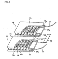
Two electronic cooling elements 16 were prepared to be mounted on the
package 11. As shown in Fig. 1, n-type thermoelectric elements (BiTiSe) 16a
and p-type thermoelectric elements (BiTeSb) 16b were arranged alternately to
form a matrix. Upper faces and lower faces of neighboring thermoelectric
elements were respectively connected in series using Pb60Sn40 solder (melting
point : 238°C) by pad 18 of copper or other materials formed on ceramic
substrates 17a and 17b made of AlN. A metallized layer of AgPd was formed on
the upper face of the ceramic substrate 17a and on the lower face of the ceramic
substrate 17b in each of electronic cooling elements 16. In addition, a layer of
BiSn solder (melting point: 160°C) was provided on the upper face thereof with
which an optical semiconductor device was to be jointed, whereas on the lower
face thereof with which the bottom plate 13 was to be jointed was provided a
layer of Pb37Sn63 solder (melting point: 183°C).
Two pads 18a and 18b were formed on the lower substrate 17b of the
electronic cooling element, and a Cu lead plated with NiSn was jointed to the
pad 18a with Pb90Sn10 solder (melting point: 299°C).
One of the two electronic cooling elements 16 was inserted through the
space between inner juts 14a of the ceramic feedthrough 14 of the package 11
into the space under one of the inner juts and placed thereunder on the bottom
plate 13. Then, another electronic cooling element was inserted through the
space between the inner juts 14a in the same manner into the space under the
other inner jut and placed thereunder on the bottom plate 13. The two
electronic cooling elements 16 were arranged close together at the center of the
bottom plate 13.
The two electronic cooling elements placed on the bottom plate 13 were
held by a carbon jig. As shown in Fig. 1, a copper piece 20 was placed on a
Pn37Sn63 (melting point: 183°C) solder layer that was formed on the pad 18b
provided on the lower ceramic substrates 17b of the electronic cooling elements.
In the state as described above, the whole package 11 was put in a continuous
hydrogen furnace of 220°C and the two electronic cooling elements 16 were
fixed to the bottom plate 13 of the package 11 and connected together in series
by the copper piece at the same time.
Thus, the package 11 whose bottom plate 13 was jointed to the two
electronic cooling elements 16 was obtained, as shown in Fig. 2. Thereafter, as
shown in Fig. 3, a circuit board 21, on which an optical semiconductor device 23
such as a laser diode element, etc. was mounted beforehand, was jointed to the
upper surface (two ceramic substrates 17a in Fig. 1) of the two electronic
cooling elements 16 with BiSn solder, which had been provided in advance, in a
nitrogen atmosphere. The circuit board 21 was provided with a sub-carrier 22
at the bottom thereof in advance so as to adjust a height position of wire
bonding. Finally, after wiring with Au wires and jointing a cap 24 onto a square
ring 15 for sealing, an optical fiber was aligned with a light transmission
window of the package 11 and welded by YAG laser. Thus, an optical
semiconductor module was completed.
In the optical semiconductor module thus obtained, the optical
semiconductor device 23 was mounted astride the two electronic cooling units
16 which were arranged closely together at the center of the bottom plate 13. In
addition, the two electronic elements 16 were jointed not only to the center part
of the bottom plate 13 but also to other parts of the bottom plate under the
inner juts 14a in the package. Accordingly, the total area of the junction
between the two electronic cooling elements 16 and the bottom plate 13
amounted to about 90% of the area of the bottom plate in the package 11.
According to the present invention, the ratio of the area of junction
between the bottom plate and electronic cooling elements to the area of the
bottom plate in the package can be increased. Therefore, an optical
semiconductor module having a large endothermic amount of the electronic
cooling element can be provided, even if the area of the bottom plate area of the
package is the same.
Claims (6)
- An optical semiconductor module comprising:a package whose frame has ceramic feedthrough;two or more units of electronic cooling element connected to the bottom plate of said package; andan optical semiconductor device mounted on said two or more units of electronic cooling element.
- An optical semiconductor module according to claim 1, wherein the area of junction between said two or more units of electronic cooling element and the bottom plate of said package occupies 75% or more of the area of the bottom plate.
- An optical semiconductor module according to claim 1 or 2, wherein said two or more units of electronic cooling element are connected in series by one or more copper piece.
- A manufacturing method of an optical semiconductor module, comprising the steps of:fixing two or more units of electronic cooling element to the bottom plate of a package whose frame has ceramic feedthrough; andmounting an optical semiconductor device on said two or more units of electronic cooling element..
- A manufacturing method of an optical semiconductor module according to claim 4, wherein said two or more units of electronic cooling element are connected in series with one or more copper piece.
- A manufacturing method of an optical semiconductor module according to claim 4 or 5, wherein said step of fixing two or more units of electronic cooling element to the bottom plate of a package and a step of connecting said two or more units of electronic cooling element with one or more copper piece are carried out simultaneously using the same solder.
Applications Claiming Priority (3)
| Application Number | Priority Date | Filing Date | Title |
|---|---|---|---|
| JP2001222508 | 2001-07-24 | ||
| JP2001222508 | 2001-07-24 | ||
| PCT/JP2002/003504 WO2003010867A1 (en) | 2001-07-24 | 2002-04-08 | Optical semiconductor module and method of producing the same |
Publications (2)
| Publication Number | Publication Date |
|---|---|
| EP1411602A1 true EP1411602A1 (en) | 2004-04-21 |
| EP1411602A4 EP1411602A4 (en) | 2005-02-23 |
Family
ID=19055981
Family Applications (1)
| Application Number | Title | Priority Date | Filing Date |
|---|---|---|---|
| EP02714546A Withdrawn EP1411602A4 (en) | 2001-07-24 | 2002-04-08 | OPTICAL SEMICONDUCTOR MODULE AND CORRESPONDING PRODUCTION METHOD |
Country Status (7)
| Country | Link |
|---|---|
| US (1) | US6855566B2 (en) |
| EP (1) | EP1411602A4 (en) |
| JP (1) | JPWO2003010867A1 (en) |
| KR (1) | KR20030060891A (en) |
| CN (1) | CN1465122A (en) |
| CA (1) | CA2423609A1 (en) |
| WO (1) | WO2003010867A1 (en) |
Cited By (3)
| Publication number | Priority date | Publication date | Assignee | Title |
|---|---|---|---|---|
| US9625671B2 (en) | 2013-10-23 | 2017-04-18 | Lasermax, Inc. | Laser module and system |
| US9859680B2 (en) | 2013-12-17 | 2018-01-02 | Lasermax, Inc. | Shock resistant laser module |
| PL451001A1 (en) * | 2025-01-20 | 2025-08-04 | Energotech Lublin Spółka Z Ograniczoną Odpowiedzialnością | Low-energy temperature stabilization system for optoelectronic components |
Families Citing this family (6)
| Publication number | Priority date | Publication date | Assignee | Title |
|---|---|---|---|---|
| US7928459B2 (en) * | 2006-02-24 | 2011-04-19 | Seoul Semiconductor Co., Ltd. | Light emitting diode package including thermoelectric element |
| JP5473535B2 (en) * | 2009-10-28 | 2014-04-16 | 三菱電機株式会社 | Light source device |
| GB2544787A (en) * | 2015-11-27 | 2017-05-31 | European Thermodynamics Ltd | Thermoelectric module |
| JP6852513B2 (en) * | 2017-03-30 | 2021-03-31 | 株式会社オートネットワーク技術研究所 | Circuit equipment |
| WO2020202789A1 (en) * | 2019-03-29 | 2020-10-08 | ソニーセミコンダクタソリューションズ株式会社 | Sensor device |
| KR20230116358A (en) * | 2022-01-28 | 2023-08-04 | 엘지이노텍 주식회사 | Thermoelectric device |
Family Cites Families (17)
| Publication number | Priority date | Publication date | Assignee | Title |
|---|---|---|---|---|
| JPS6022345A (en) | 1983-07-19 | 1985-02-04 | Toyota Central Res & Dev Lab Inc | Semiconductor device |
| JPH02132874A (en) | 1988-11-14 | 1990-05-22 | Fujitsu Ltd | Temperature stabilizing laser diode module |
| US4930857A (en) | 1989-05-19 | 1990-06-05 | At&T Bell Laboratories | Hybrid package arrangement |
| JP3276418B2 (en) * | 1992-09-24 | 2002-04-22 | 浜松ホトニクス株式会社 | Image tube equipment |
| JPH0888428A (en) * | 1994-09-20 | 1996-04-02 | Fuji Photo Film Co Ltd | Laser diode pumping solid state laser |
| EP0774684A3 (en) * | 1995-11-16 | 1998-04-22 | Matsushita Electric Industrial Co., Ltd. | Optical apparatus and method for producing the same |
| JPH09229765A (en) * | 1996-02-28 | 1997-09-05 | Mitsubishi Electric Corp | Infrared detector |
| JPH10284804A (en) | 1997-04-07 | 1998-10-23 | Furukawa Electric Co Ltd:The | Semiconductor laser module |
| EP0899795A3 (en) | 1997-08-27 | 1999-05-12 | Sumitomo Electric Industries, Ltd. | Optical-semiconductor container or module |
| JP3176334B2 (en) | 1998-01-21 | 2001-06-18 | 京セラ株式会社 | Package for storing optical semiconductor element and method for manufacturing the same |
| JP4180140B2 (en) | 1998-02-12 | 2008-11-12 | 富士通株式会社 | Multi-wavelength light source |
| JPH11295560A (en) * | 1998-04-09 | 1999-10-29 | Matsushita Electric Ind Co Ltd | Optical communication module and inspection method thereof |
| WO2000037314A1 (en) * | 1998-12-21 | 2000-06-29 | Alliedsignal Inc. | Ir diode based high intensity light |
| EP1069659A4 (en) * | 1999-02-03 | 2003-03-05 | Furukawa Electric Co Ltd | Semiconductor laser and semiconductor laser module using the same |
| JP2000340874A (en) | 1999-05-31 | 2000-12-08 | Matsushita Electric Ind Co Ltd | Semiconductor laser module |
| US20040014341A1 (en) * | 2001-04-05 | 2004-01-22 | Akira Katou | Connection structure of connector pin and signal line and semiconductor package using it |
| JP3901570B2 (en) * | 2002-04-23 | 2007-04-04 | スパンション エルエルシー | Low temperature testing equipment for semiconductor devices using electronic cooling elements |
-
2002
- 2002-04-06 US US10/381,460 patent/US6855566B2/en not_active Expired - Fee Related
- 2002-04-08 KR KR10-2003-7003526A patent/KR20030060891A/en not_active Ceased
- 2002-04-08 WO PCT/JP2002/003504 patent/WO2003010867A1/en not_active Ceased
- 2002-04-08 EP EP02714546A patent/EP1411602A4/en not_active Withdrawn
- 2002-04-08 JP JP2002589142A patent/JPWO2003010867A1/en not_active Withdrawn
- 2002-04-08 CN CN02802460A patent/CN1465122A/en active Pending
- 2002-04-08 CA CA002423609A patent/CA2423609A1/en not_active Abandoned
Cited By (4)
| Publication number | Priority date | Publication date | Assignee | Title |
|---|---|---|---|---|
| US9625671B2 (en) | 2013-10-23 | 2017-04-18 | Lasermax, Inc. | Laser module and system |
| US11018476B2 (en) | 2013-10-23 | 2021-05-25 | Lmd Applied Science, Llc | Laser module and system |
| US9859680B2 (en) | 2013-12-17 | 2018-01-02 | Lasermax, Inc. | Shock resistant laser module |
| PL451001A1 (en) * | 2025-01-20 | 2025-08-04 | Energotech Lublin Spółka Z Ograniczoną Odpowiedzialnością | Low-energy temperature stabilization system for optoelectronic components |
Also Published As
| Publication number | Publication date |
|---|---|
| JPWO2003010867A1 (en) | 2004-11-18 |
| US6855566B2 (en) | 2005-02-15 |
| CA2423609A1 (en) | 2003-03-24 |
| CN1465122A (en) | 2003-12-31 |
| US20040013152A1 (en) | 2004-01-22 |
| EP1411602A4 (en) | 2005-02-23 |
| KR20030060891A (en) | 2003-07-16 |
| WO2003010867A1 (en) | 2003-02-06 |
Similar Documents
| Publication | Publication Date | Title |
|---|---|---|
| US7391153B2 (en) | Light emitting device provided with a submount assembly for improved thermal dissipation | |
| US7968980B2 (en) | Support member for mounting a semiconductor device, conductive materials, and its manufacturing method | |
| US7078801B2 (en) | Thermoelectric module package | |
| EP1187196B1 (en) | Method of manufacturing an optical semiconductor module | |
| US6855566B2 (en) | Optical semiconductor module and method of producing the same | |
| JP2001168443A (en) | Package for storing optical semiconductor elements | |
| JP4116809B2 (en) | Thermoelectric element module, semiconductor element storage package and semiconductor module | |
| JP2004303750A (en) | Package for thermoelectric device and method of manufacturing the same | |
| JP2002270906A (en) | Thermoelectric module | |
| JP4005937B2 (en) | Thermoelectric module package | |
| JP3810276B2 (en) | Optical semiconductor element storage package | |
| US6600223B2 (en) | Hermetically sealing enclosure for housing photo-semiconductor devices and photo-semiconductor module incorporating the enclosure | |
| JP4009110B2 (en) | Optical semiconductor element storage package and optical semiconductor device | |
| WO2003025652A1 (en) | Hermetically sealed package container for optical module | |
| JP7196249B2 (en) | Packages for semiconductor devices and semiconductor devices | |
| JP3860831B2 (en) | Optical semiconductor element storage package | |
| JP3909253B2 (en) | Thermoelectric element module, semiconductor element storage package and semiconductor module | |
| JP2003318451A (en) | Thermoelectric element module, semiconductor element storage package and semiconductor module | |
| HK1058109A (en) | Optical semiconductor module and method of producing the same | |
| JP2003152231A (en) | Thermoelectric element module, semiconductor element storage package and semiconductor module | |
| JP2003179293A (en) | Package for storing optical semiconductor elements | |
| JP2003258357A (en) | Optical semiconductor element storage package | |
| JP2003158303A (en) | Thermoelectric element module, semiconductor element storage package and semiconductor module | |
| JP2003197987A (en) | Thermoelectric element module, semiconductor element storage package and semiconductor module | |
| JP2002076495A (en) | Hermetically sealed optical semiconductor container |
Legal Events
| Date | Code | Title | Description |
|---|---|---|---|
| PUAI | Public reference made under article 153(3) epc to a published international application that has entered the european phase |
Free format text: ORIGINAL CODE: 0009012 |
|
| 17P | Request for examination filed |
Effective date: 20030403 |
|
| AK | Designated contracting states |
Kind code of ref document: A1 Designated state(s): AT BE CH CY DE DK ES FI FR GB GR IE IT LI LU MC NL PT SE TR |
|
| AX | Request for extension of the european patent |
Extension state: AL LT LV MK RO SI |
|
| A4 | Supplementary search report drawn up and despatched |
Effective date: 20050110 |
|
| 17Q | First examination report despatched |
Effective date: 20050310 |
|
| STAA | Information on the status of an ep patent application or granted ep patent |
Free format text: STATUS: THE APPLICATION IS DEEMED TO BE WITHDRAWN |
|
| 18D | Application deemed to be withdrawn |
Effective date: 20050721 |