EP1408087A1 - Epoxy-polysiloxane resin compositions, solid state devices encapsulated therewith and method - Google Patents
Epoxy-polysiloxane resin compositions, solid state devices encapsulated therewith and method Download PDFInfo
- Publication number
- EP1408087A1 EP1408087A1 EP20030256305 EP03256305A EP1408087A1 EP 1408087 A1 EP1408087 A1 EP 1408087A1 EP 20030256305 EP20030256305 EP 20030256305 EP 03256305 A EP03256305 A EP 03256305A EP 1408087 A1 EP1408087 A1 EP 1408087A1
- Authority
- EP
- European Patent Office
- Prior art keywords
- weight
- anhydride
- present
- epoxy resin
- silicone resin
- Prior art date
- Legal status (The legal status is an assumption and is not a legal conclusion. Google has not performed a legal analysis and makes no representation as to the accuracy of the status listed.)
- Granted
Links
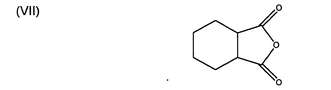
- MUTGBJKUEZFXGO-UHFFFAOYSA-N O=C(C1C2CCCC1)OC2=O Chemical compound O=C(C1C2CCCC1)OC2=O MUTGBJKUEZFXGO-UHFFFAOYSA-N 0.000 description 2
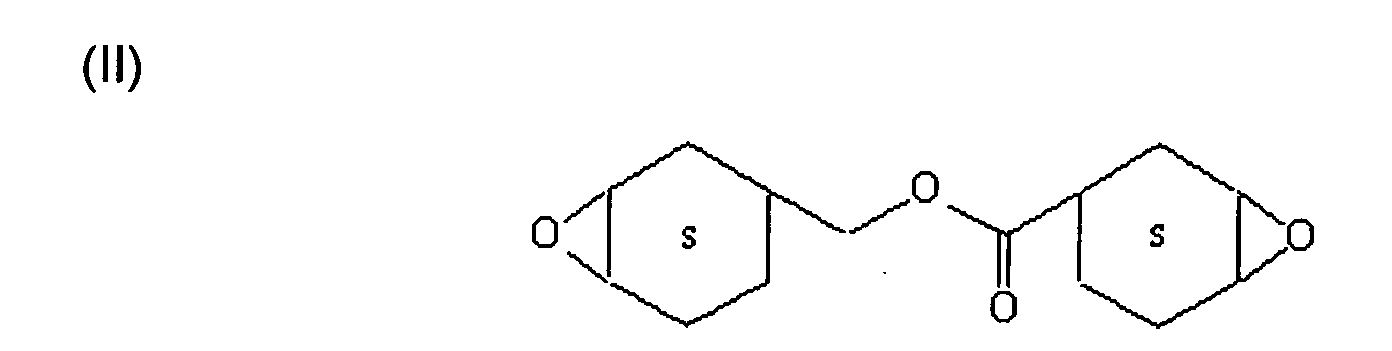
- RMKPMVVPYQNAOK-VQHVLOKHSA-N O=C(C1C=C2OC2CC1)O/C=C1/C2OC2CCC1 Chemical compound O=C(C1C=C2OC2CC1)O/C=C1/C2OC2CCC1 RMKPMVVPYQNAOK-VQHVLOKHSA-N 0.000 description 1
Images



Classifications
-
- C—CHEMISTRY; METALLURGY
- C08—ORGANIC MACROMOLECULAR COMPOUNDS; THEIR PREPARATION OR CHEMICAL WORKING-UP; COMPOSITIONS BASED THEREON
- C08L—COMPOSITIONS OF MACROMOLECULAR COMPOUNDS
- C08L63/00—Compositions of epoxy resins; Compositions of derivatives of epoxy resins
-
- C—CHEMISTRY; METALLURGY
- C08—ORGANIC MACROMOLECULAR COMPOUNDS; THEIR PREPARATION OR CHEMICAL WORKING-UP; COMPOSITIONS BASED THEREON
- C08G—MACROMOLECULAR COMPOUNDS OBTAINED OTHERWISE THAN BY REACTIONS ONLY INVOLVING UNSATURATED CARBON-TO-CARBON BONDS
- C08G59/00—Polycondensates containing more than one epoxy group per molecule; Macromolecules obtained by polymerising compounds containing more than one epoxy group per molecule using curing agents or catalysts which react with the epoxy groups
- C08G59/18—Macromolecules obtained by polymerising compounds containing more than one epoxy group per molecule using curing agents or catalysts which react with the epoxy groups ; e.g. general methods of curing
- C08G59/40—Macromolecules obtained by polymerising compounds containing more than one epoxy group per molecule using curing agents or catalysts which react with the epoxy groups ; e.g. general methods of curing characterised by the curing agents used
- C08G59/42—Polycarboxylic acids; Anhydrides, halides or low molecular weight esters thereof
- C08G59/4284—Polycarboxylic acids; Anhydrides, halides or low molecular weight esters thereof together with other curing agents
-
- C—CHEMISTRY; METALLURGY
- C08—ORGANIC MACROMOLECULAR COMPOUNDS; THEIR PREPARATION OR CHEMICAL WORKING-UP; COMPOSITIONS BASED THEREON
- C08L—COMPOSITIONS OF MACROMOLECULAR COMPOUNDS
- C08L83/00—Compositions of macromolecular compounds obtained by reactions forming in the main chain of the macromolecule a linkage containing silicon with or without sulfur, nitrogen, oxygen or carbon only; Compositions of derivatives of such polymers
- C08L83/04—Polysiloxanes
-
- C—CHEMISTRY; METALLURGY
- C08—ORGANIC MACROMOLECULAR COMPOUNDS; THEIR PREPARATION OR CHEMICAL WORKING-UP; COMPOSITIONS BASED THEREON
- C08G—MACROMOLECULAR COMPOUNDS OBTAINED OTHERWISE THAN BY REACTIONS ONLY INVOLVING UNSATURATED CARBON-TO-CARBON BONDS
- C08G77/00—Macromolecular compounds obtained by reactions forming a linkage containing silicon with or without sulfur, nitrogen, oxygen or carbon in the main chain of the macromolecule
- C08G77/04—Polysiloxanes
- C08G77/045—Polysiloxanes containing less than 25 silicon atoms
-
- C—CHEMISTRY; METALLURGY
- C08—ORGANIC MACROMOLECULAR COMPOUNDS; THEIR PREPARATION OR CHEMICAL WORKING-UP; COMPOSITIONS BASED THEREON
- C08G—MACROMOLECULAR COMPOUNDS OBTAINED OTHERWISE THAN BY REACTIONS ONLY INVOLVING UNSATURATED CARBON-TO-CARBON BONDS
- C08G77/00—Macromolecular compounds obtained by reactions forming a linkage containing silicon with or without sulfur, nitrogen, oxygen or carbon in the main chain of the macromolecule
- C08G77/04—Polysiloxanes
- C08G77/12—Polysiloxanes containing silicon bound to hydrogen
-
- C—CHEMISTRY; METALLURGY
- C08—ORGANIC MACROMOLECULAR COMPOUNDS; THEIR PREPARATION OR CHEMICAL WORKING-UP; COMPOSITIONS BASED THEREON
- C08G—MACROMOLECULAR COMPOUNDS OBTAINED OTHERWISE THAN BY REACTIONS ONLY INVOLVING UNSATURATED CARBON-TO-CARBON BONDS
- C08G77/00—Macromolecular compounds obtained by reactions forming a linkage containing silicon with or without sulfur, nitrogen, oxygen or carbon in the main chain of the macromolecule
- C08G77/04—Polysiloxanes
- C08G77/14—Polysiloxanes containing silicon bound to oxygen-containing groups
- C08G77/16—Polysiloxanes containing silicon bound to oxygen-containing groups to hydroxy groups
-
- C—CHEMISTRY; METALLURGY
- C08—ORGANIC MACROMOLECULAR COMPOUNDS; THEIR PREPARATION OR CHEMICAL WORKING-UP; COMPOSITIONS BASED THEREON
- C08G—MACROMOLECULAR COMPOUNDS OBTAINED OTHERWISE THAN BY REACTIONS ONLY INVOLVING UNSATURATED CARBON-TO-CARBON BONDS
- C08G77/00—Macromolecular compounds obtained by reactions forming a linkage containing silicon with or without sulfur, nitrogen, oxygen or carbon in the main chain of the macromolecule
- C08G77/04—Polysiloxanes
- C08G77/14—Polysiloxanes containing silicon bound to oxygen-containing groups
- C08G77/18—Polysiloxanes containing silicon bound to oxygen-containing groups to alkoxy or aryloxy groups
-
- C—CHEMISTRY; METALLURGY
- C08—ORGANIC MACROMOLECULAR COMPOUNDS; THEIR PREPARATION OR CHEMICAL WORKING-UP; COMPOSITIONS BASED THEREON
- C08G—MACROMOLECULAR COMPOUNDS OBTAINED OTHERWISE THAN BY REACTIONS ONLY INVOLVING UNSATURATED CARBON-TO-CARBON BONDS
- C08G77/00—Macromolecular compounds obtained by reactions forming a linkage containing silicon with or without sulfur, nitrogen, oxygen or carbon in the main chain of the macromolecule
- C08G77/04—Polysiloxanes
- C08G77/20—Polysiloxanes containing silicon bound to unsaturated aliphatic groups
-
- C—CHEMISTRY; METALLURGY
- C08—ORGANIC MACROMOLECULAR COMPOUNDS; THEIR PREPARATION OR CHEMICAL WORKING-UP; COMPOSITIONS BASED THEREON
- C08G—MACROMOLECULAR COMPOUNDS OBTAINED OTHERWISE THAN BY REACTIONS ONLY INVOLVING UNSATURATED CARBON-TO-CARBON BONDS
- C08G77/00—Macromolecular compounds obtained by reactions forming a linkage containing silicon with or without sulfur, nitrogen, oxygen or carbon in the main chain of the macromolecule
- C08G77/70—Siloxanes defined by use of the MDTQ nomenclature
-
- H—ELECTRICITY
- H10—SEMICONDUCTOR DEVICES; ELECTRIC SOLID-STATE DEVICES NOT OTHERWISE PROVIDED FOR
- H10H—INORGANIC LIGHT-EMITTING SEMICONDUCTOR DEVICES HAVING POTENTIAL BARRIERS
- H10H20/00—Individual inorganic light-emitting semiconductor devices having potential barriers, e.g. light-emitting diodes [LED]
- H10H20/80—Constructional details
- H10H20/85—Packages
- H10H20/852—Encapsulations
- H10H20/854—Encapsulations characterised by their material, e.g. epoxy or silicone resins
-
- H—ELECTRICITY
- H10—SEMICONDUCTOR DEVICES; ELECTRIC SOLID-STATE DEVICES NOT OTHERWISE PROVIDED FOR
- H10W—GENERIC PACKAGES, INTERCONNECTIONS, CONNECTORS OR OTHER CONSTRUCTIONAL DETAILS OF DEVICES COVERED BY CLASS H10
- H10W74/00—Encapsulations, e.g. protective coatings
-
- H—ELECTRICITY
- H10—SEMICONDUCTOR DEVICES; ELECTRIC SOLID-STATE DEVICES NOT OTHERWISE PROVIDED FOR
- H10W—GENERIC PACKAGES, INTERCONNECTIONS, CONNECTORS OR OTHER CONSTRUCTIONAL DETAILS OF DEVICES COVERED BY CLASS H10
- H10W90/00—Package configurations
- H10W90/701—Package configurations characterised by the relative positions of pads or connectors relative to package parts
- H10W90/751—Package configurations characterised by the relative positions of pads or connectors relative to package parts of bond wires
- H10W90/756—Package configurations characterised by the relative positions of pads or connectors relative to package parts of bond wires between a chip and a stacked lead frame, conducting package substrate or heat sink
-
- Y—GENERAL TAGGING OF NEW TECHNOLOGICAL DEVELOPMENTS; GENERAL TAGGING OF CROSS-SECTIONAL TECHNOLOGIES SPANNING OVER SEVERAL SECTIONS OF THE IPC; TECHNICAL SUBJECTS COVERED BY FORMER USPC CROSS-REFERENCE ART COLLECTIONS [XRACs] AND DIGESTS
- Y10—TECHNICAL SUBJECTS COVERED BY FORMER USPC
- Y10T—TECHNICAL SUBJECTS COVERED BY FORMER US CLASSIFICATION
- Y10T428/00—Stock material or miscellaneous articles
- Y10T428/31504—Composite [nonstructural laminate]
- Y10T428/31511—Of epoxy ether
-
- Y—GENERAL TAGGING OF NEW TECHNOLOGICAL DEVELOPMENTS; GENERAL TAGGING OF CROSS-SECTIONAL TECHNOLOGIES SPANNING OVER SEVERAL SECTIONS OF THE IPC; TECHNICAL SUBJECTS COVERED BY FORMER USPC CROSS-REFERENCE ART COLLECTIONS [XRACs] AND DIGESTS
- Y10—TECHNICAL SUBJECTS COVERED BY FORMER USPC
- Y10T—TECHNICAL SUBJECTS COVERED BY FORMER US CLASSIFICATION
- Y10T428/00—Stock material or miscellaneous articles
- Y10T428/31504—Composite [nonstructural laminate]
- Y10T428/31652—Of asbestos
- Y10T428/31663—As siloxane, silicone or silane
Definitions
- This invention relates to epoxy resin compositions and solid state devices encapsulated therewith.
- the invention also relates to a method for encapsulating a solid state device.
- a method of encapsulating a solid state device comprising placing the solid state device into an encapsulating composition comprising (A) at least one silicone resin, (B) at least one epoxy resin, (C) at least one anhydride curing agent, (D) at least one siloxane surfactant, and (E) at least one ancillary curing catalyst.
- Silicone resins useful as component (A) in the present invention comprise those given in structure (I) below.
- the silicone resin can be a branched structure in which R may be an OSiR 3 substituent, where R 3 can be hydroxyl, C 1-22 alkyl, C 1-22 alkoxy, C 2-22 alkenyl, C 6-14 aryl, C 6-22 alkyl-substituted aryl, and C 6-22 aralkyl.
- epoxy resins produced by reaction of a compound containing at least one and preferably two or more carbon-carbon double bond with a peroxide, for example, a peroxyacid.
- examples of epoxy resins useful in the present invention include aliphatic epoxy resins, cycloaliphatic epoxy resins, bisphenol-A epoxy resins, bisphenol-F epoxy resins, phenol novolac epoxy resins, cresol-novolac epoxy resins, biphenyl epoxy resins, biphenyl epoxy resins, 4,4'-biphenyl epoxy resins, polyfunctional epoxy resins, divinylbenzene dioxide, and 2-glycidylphenylglycidyl ether.
- epoxy resins can be used singly or in a combination of at least two epoxy resins.
- Preferred epoxy resins for the present invention are cycloaliphatic epoxy resins and aliphatic epoxy resins.
- Aliphatic epoxy resins include compounds that contain at least one aliphatic group and at least one epoxy group.
- Examples of aliphatic epoxies include, butadiene dioxide, dimethylpentane dioxide, diglycidyl ether, 1,4-butanedioldiglycidyl ether, diethylene glycol diglycidyl ether, and dipentene dioxide.
- Examples include 2-(3,4-epoxy)cyclohexyl-5, 5-spiro-(3,4-epoxy)cyclohexane- m -dioxane,3,4-epoxycyclohexylalkyl-3,4-epoxycyclohexanecarboxylate, 3,4-epoxy-6-methylcyclohexylmethyl-3,4-epoxy-6-methylcyclohexanecarboxylate, vinyl cyclohexanedioxide, bis(3,4-epoxycyclohexylmethyl)adipate, bis(3,4-epoxy-6-methylcyclohexylmethyl)adipate, exo-exo bis(2,3-epoxycyclopentyl) ether, endo-exo bis(2,3-epoxycyclopentyl) ether, 2,2-bis(4-(2,3-epoxypropoxy)cyclohexyl)propane, 2,6-bis(2,3
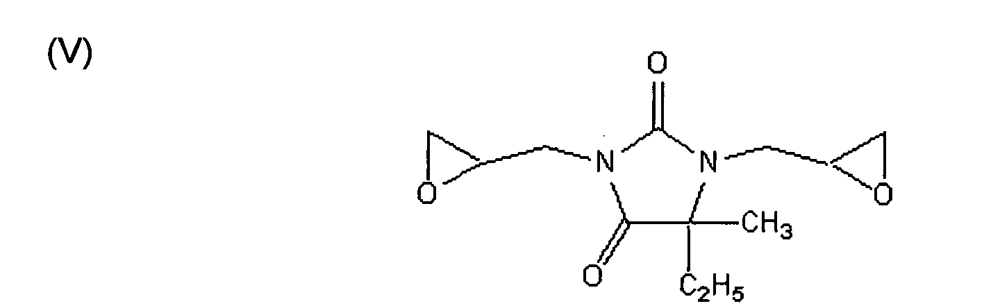
- Additional exemplary epoxy resins (B) of the present invention include those of structure (II), (III), (IV), and (V) given below.
- Additives such as thermal stabilizers or antioxidants maybe used with aromatic epoxy resins to lessen discoloring.
- Flexibilizers are useful in the composition to reduce brittleness and include aliphatic epoxy resins, siloxane resins, and the like.
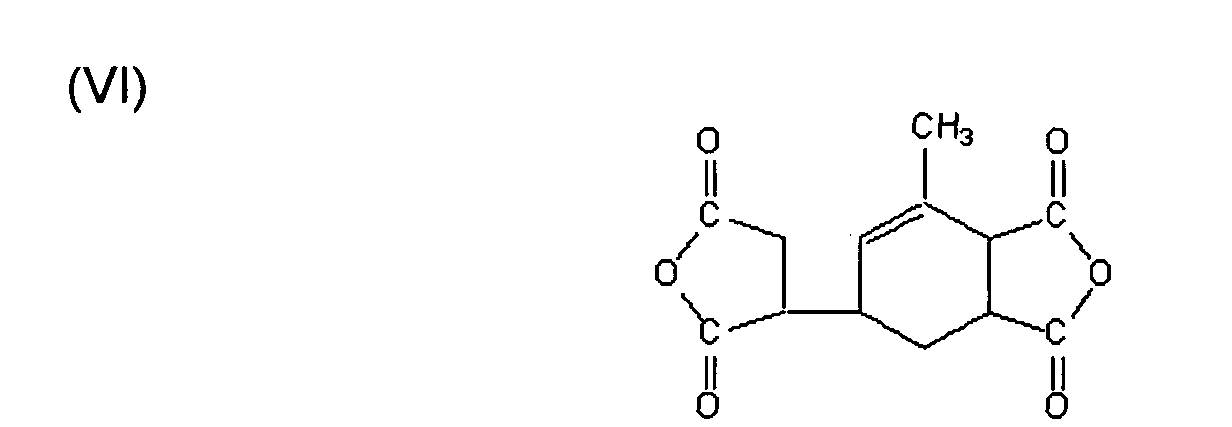
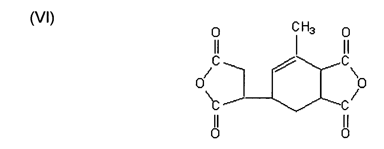
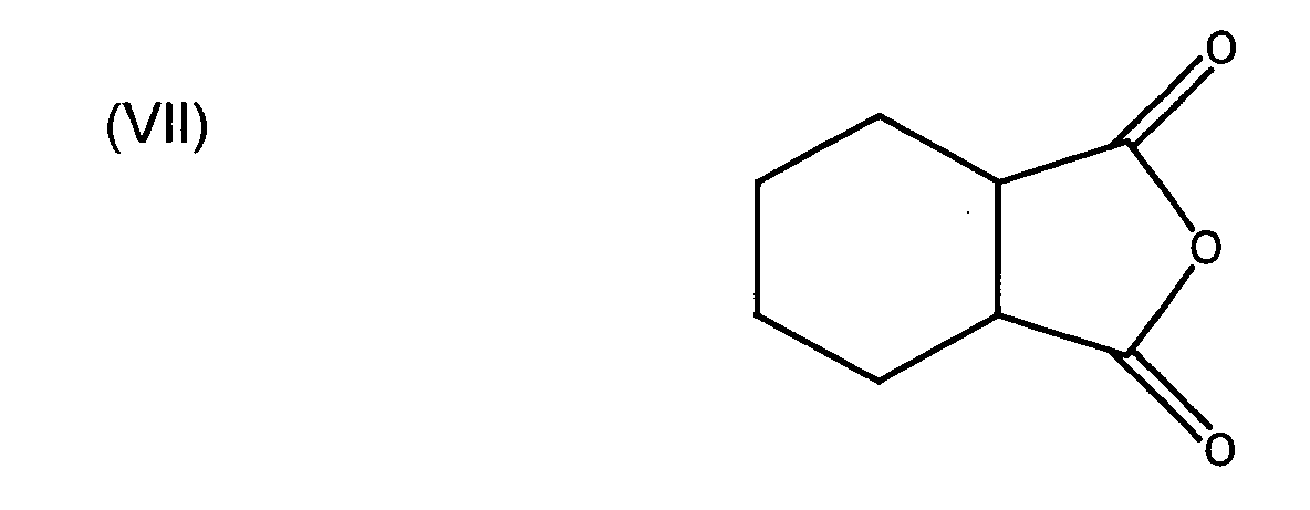
- Exemplary anhydride curing agents useful as component (C) typically include those of structures (VI) and (VII) below and bicyclo[2.2.1]hept-5-ene-2,3-dicarboxylic anhydride, methylbicyclo[2.2.1]hept-5-ene-2,3-dicarboxylic anhydride, bicyclo[2.2.1]hept-5-ene-2,3-dicarboxylic anhydride, phthalic anhydride, pyromellitic dianhydride, hexahydrophthalic anhydride, hexahydro-4-methylphthalic anhydride, dodecenylsuccinic anhydride, dichloromaleic anhydride, chlorendic anhydride, tetrachlorophthalic anhydride, and the like.
- Mixtures comprising at least two anhydride curing agents may also be used.
- Illustrative examples are described in “Chemistry and Technology of the Epoxy Resins” B. Ellis (Ed.) Chapman Hall, New York, 1993 and in “Epoxy Resins Chemistry and Technology", edited by C. A. May, Marcel Dekker, New York, 2nd edition, 1988.
- siloxane surfactants (D) it is possible to blend various components in the encapsulating composition resulting in homogeneity, clarity, low scattering properties, moisture resistance, and flexibility in addition to making the composition shatter proof.
- Siloxane surfactants are used to compatibilize the various materials used in the present invention.
- Siloxane surfactants may be used to compatibilize incompatible material into one homogeneous phase (i.e. uniform phase) by a reduction of interfacial tension to give desirable and required properties.
- the silicone resin may be compatibilized with the epoxy resin using the siloxane surfactant.
- the siloxane surfactants used in the present invention may be functionalized with polyethylene glycol, polypropylene glycol, polypropylene glycol ethers and substituted siloxane polymers.
- the surfactants may be used singly or in combination thereof.
- the siloxane surfactants of the present invention may be used to compatibilize the silicone resin with the epoxy resin, curing agents, and optional refractive index modifiers and thermal stabilizers into one homogeneous composition which, when cured may give an encapsulant composition which may be clear and transparent with moisture resistance, solvent resistance, crack resistance properties, heat resistance, as well as UV absorption and light transmission in given wavelength ranges.
- the values of x and y in structure (VIII) may be in a range between about 5 to about 10.
- the percentage of silicon in the surfactant typically may be in a range between about 10% by weight and about 80% by weight of the total weight of the siloxane surfactant in one embodiment of the present invention, while it may be in a range between about 20% by weight and about 60% by weight of the total weight of the siloxane surfactant in a second embodiment of the invention.
- the silicon content may be in a range between about 25% and about 50% by weight of the total weight of the siloxane surfactant.
- the ancillary curing catalyst comprises at least one of a metal carboxylate, a metal acetylacetonate, zinc octoate, stannous octoate, triarylsulfonium hexafluorophosphate, triarylsulfonium hexafluoroantimonate (such as CD 1010 sold by Sartomer Corporation), diaryliodonium hexafluoroantimonate, or diaryliodonium tetrakis(pentafluorophenyl)borate.
- a metal carboxylate a metal acetylacetonate
- zinc octoate zinc octoate
- stannous octoate triarylsulfonium hexafluorophosphate
- triarylsulfonium hexafluoroantimonate such as CD 1010 sold by Sartomer Corporation
- diaryliodonium hexafluoroantimonate diarylio
- silicone resin (A), epoxy resin (B), anhydride curing agent (C), siloxane surfactant (D), and ancillary curing catalyst (E) can be varied over a wide range.
- the amount of silicone resin (A) in the composition is greater than about 40% by weight based on the combined weight of the silicone resin (A), epoxy resin (B), anhydride curing gent (C), siloxane surfactant (D), and ancillary curing catalyst (E).
- the amount of silicone resin (A) in the composition is in a range of between about 40% by weight and about 99% by weight based on the combined weight of silicone resin (A), epoxy resin (B), anhydride curing agent (C), siloxane surfactant (D), and ancillary curing catalyst (E). In other embodiments, the amount of silicone resin (A) in the composition is in a range of between about 76% by weight and about 99% by weight based on the combined weight of silicone resin (A), epoxy resin (B), anhydride curing agent (C), siloxane surfactant (D), and ancillary curing catalyst (E).
- the silicone resin, epoxy resin, the siloxane surfactant, the anhydride curing agent, and the ancillary curing catalyst are mixed in to give an encapsulating composition and the composition is cured and polished, the resulting surface may be transparent and clear and the encapsulant material may be crack-proof and may not scatter light.
- the amount of ancillary curing catalyst (E) in the composition is in a range between about 0.01% by weight and about 0.5% by weight based on the combined weight of silicone resin (A), epoxy resin (B), anhydride curing agent (C), siloxane surfactant (D) and ancillary curing catalyst (E).
- These materials comprise optically transparent organics or inorganics such as silicone fluids, and agglomerates of particles or structures whose size is less than the size of the wavelength of the emitted light. Such agglomerates are sometimes referred to as nanoparticles.
- agglomerates comprise a variety of transparent metal oxides or Group II-VI materials that are relatively free from scattering.
- a nanoparticle material is titanium dioxide.
- other types of transparent metal oxides or combinations of metal oxides can be used.
- magnesium oxide, yttria, zirconia, cerium oxides, alumina, lead oxides, and composite materials such as those comprising yttria and zirconia can be used to produce nanoparticles.
- nanoparticles are made from one of the Group II-VI materials comprising zinc selenide, zinc sulphide, and alloys made from Zn, Se, S, and Te.
- gallium nitride, silicon nitride, or aluminum nitride can be also used to make nanoparticles.
- Refractive index modifiers can be used singly or in a combination of at least two compounds.
- the refractive index of the encapsulating composition is in a range between about 0.1 and about 10.0.
- the refractive index is in a range between about 0.5 and about 5.0 and in a third embodiment, the refractive index is in a range between about 1.0 and about 2.5. In many embodiments, the refractive index is in a range between about 1.0 and about 2.0.
- Encapsulation techniques for solid-state devices comprise casting, resin transfer molding and the like. After the solid-state device is enveloped in the uncured resin, typically performed in a mold, the resin is cured. These resins may be cured in one or more stages using methods such as thermal, UV, electron beam techniques, or combinations thereof. For example, thermal cure may be performed at temperatures in one embodiment in a range of between 20°C and about 200°C, in another embodiment in a range between about 80°C and about 200°C, in another embodiment in a range between about 100°C and about 200°C, and in another embodiment in a range between about 120°C and about 160°C. Also in other embodiments these materials can be photo-chemically cured, initially at about room temperature.
- these materials may be cured in two stages wherein an initial thermal or UV cure, for example, may be used to produce a partially hardened or B-staged epoxy resin. This material, which is easily handled, may then be further cured using, for example, either thermal or UV techniques, to produce a material with the desired thermal performance (for example glass transition temperature (Tg) and coefficient of thermal expansion (CTE)), optical properties and moisture resistance required for encapsulated solid state devices.
- an initial thermal or UV cure for example, may be used to produce a partially hardened or B-staged epoxy resin.
- This material which is easily handled, may then be further cured using, for example, either thermal or UV techniques, to produce a material with the desired thermal performance (for example glass transition temperature (Tg) and coefficient of thermal expansion (CTE)), optical properties and moisture resistance required for encapsulated solid state devices.
- Tg glass transition temperature
- CTE coefficient of thermal expansion
- the coefficient of thermal expansion when measured below the glass transition temperature varies in a range between about 50 and about 300 in one embodiment of the present invention while in a second embodiment the coefficient of thermal expansion varies in a range between about 100 and about 275 and in a third embodiment the coefficient of thermal expansion varies in a range between about 150 and about 250.
- the silicone resin (A), the epoxy resin (B), the siloxane surfactant (D), the anhydride curing agent (C), and the ancillary curing catalyst (E) when mixed into an encapsulating composition may give desirable glass transition values.
- the glass transition temperature of the composition is in a range between about 10°C and about 250°C while in a second embodiment the glass transition is in a range between about 20°C and about 200°C.
- the glass transition of the encapsulating composition varies in a range between about 24°C and about 150°C.
- the LED chip 4 emits radiation from the radiation emitting surface 9.
- the LED 1 may emit visible, ultraviolet or infrared radiation.
- the LED chip 4 may comprise any LED chip 4 containing a p-n junction of any semiconductor layers capable of emitting the desired radiation.
- the LED chip 4 may contain any desired Group III-V compound semiconductor layers, such as GaAs, GaAlAs, GaN, InGaN, GaP, etc., or Group II-VI compound semiconductor layers such ZnSe, ZnSSe, CdTe, etc., or Group IV-IV semiconductor layers, such as SiC.
- the LED chip 4 may also contain other layers, such as cladding layers, waveguide layers and contact layers.
- the LED 1 is packaged with an encapsulant 11 of the present invention.
- An alternative term for encapsulant is encapsulating material.
- the LED packaging includes encapsulant 11 located in a package, such as a shell 14.
- the shell 14 may be any plastic or other material, such as polycarbonate, which is transparent to the LED radiation.
- the shell 14 may be omitted to simplify processing if encapsulant 11 has sufficient toughness and rigidity to be used without a shell 14.
- the outer surface of encapsulant 11 would act in some embodiments as a shell 14 or package.
- the shell 14 contains a light or radiation emitting surface 15 above the LED chip 4 and a non-emitting surface 16 adjacent to the lead frame 5.
Landscapes
- Chemical & Material Sciences (AREA)
- Health & Medical Sciences (AREA)
- Chemical Kinetics & Catalysis (AREA)
- Medicinal Chemistry (AREA)
- Polymers & Plastics (AREA)
- Organic Chemistry (AREA)
- Epoxy Resins (AREA)
- Structures Or Materials For Encapsulating Or Coating Semiconductor Devices Or Solid State Devices (AREA)
- Compositions Of Macromolecular Compounds (AREA)
- Led Device Packages (AREA)
Abstract
Description
- This invention relates to epoxy resin compositions and solid state devices encapsulated therewith. The invention also relates to a method for encapsulating a solid state device.
- Solid state devices, sometimes referred to as semiconductor devices or opto-electronic devices, comprise light emitting diodes (LEDs), charge coupled devices (CCDs), large scale integrations (LSIs), photodiodes, vertical cavity surface emitting lasers (VCSELs), phototransistors, photocouplers, opto-electronic couplers and the like. Such devices often exhibit special packaging needs. High-efficiency, high lumen, solid-state white LEDs require a novel packaging material which can withstand more demanding conditions than those required by typical low-intensity, longer wavelength LEDs. Common packaging materials will often undergo a gradual loss of optical and mechanical properties due to the combination of thermal, oxidative and photodegradation processes.
- There is thus a continuing need for novel packaging material for solid state devices, such packaging material desirably possessing properties such as high transmission in a range from near UV to the visible wavelength, long-term thermal stability, oxidative stability, UV stability, thermal compliance, moisture resistance, transparency, crack resistance, polishability characteristics, compatibility with other materials used to envelope the solid state device with low color, and high reflective index.
- The present inventors have discovered curable resin compositions ideally suited for an encapsulation of solid state devices such as light emitting diodes. In one embodiment, the present invention relates to a curable epoxy resin composition for encapsulation of a solid state device, which comprises (A) at least one silicone resin, (B) at least one epoxy resin, (C) at least one anhydride curing agent, (D) at least one siloxane surfactant, and (E) at least one ancillary curing catalyst.
- In another embodiment of the present invention, there is provided a packaged solid state device comprising: (a) a package; (b) a chip; and (c) an encapsulant comprising: (A) at least one silicone resin, (B) at least one epoxy resin, (C) at least one anhydride curing agent, (D) at least one siloxane surfactant, and (E) at least one ancillary curing catalyst.
- In another embodiment of the present invention, there is provided a method of encapsulating a solid state device comprising placing the solid state device into an encapsulating composition comprising (A) at least one silicone resin, (B) at least one epoxy resin, (C) at least one anhydride curing agent, (D) at least one siloxane surfactant, and (E) at least one ancillary curing catalyst.
- The invention will now be described in greater detail, by way of example, with reference to the drawings, in which:-
- Figure 1 shows a schematic diagram of an LED device.
- Figure 2 shows a schematic diagram of a vertical cavity surface emitting laser device.
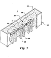
- Figure 3 shows a schematic diagram of an LED array on a plastic substrate.
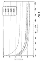
- Figure 4 shows UV-VIS-Near IR transmission data for silicone containing epoxy blends.
- Figure 5 shows UV-VIS absorption spectra for silicone containing epoxy blends.
- Figure 6 shows refractive index against wavelength data for silicone containing epoxy blends.
-
- The inventors of the present invention have determined that by using siloxane surfactants it is possible to compatibilize silicone resins with epoxy resins to make an encapsulant for a solid state device which has clarity, optimum glass transition characteristics, desirable thermal expansion characteristics, moisture resistance, refractive index values as well as transmission characteristics at particular wavelengths. The encapsulant composition comprises (A) at least one silicone resin, (B) at least one epoxy resin, (C) at least one anhydride curing agent, (D) at least one siloxane surfactant, and (E) at least one ancillary curing catalyst. Coatings using these encapsulant compositions provide moisture penetration resistance as well as heat resistance. The obtained composition may also be used as adhesives and dielectrics for multichip module fabrication. The adhesive is used for attaching chips onto a substrate or flex, as an adhesive for laminating a dielectric film such as Kapton, and as a dielectric or top layer providing a moisture resistant and abrasion resistant protection layer. The obtained formulations may also be used as encapsulants for embedding devices in multichip module fabrication.
- Silicone resins useful as component (A) in the present invention comprise those given in structure (I) below.
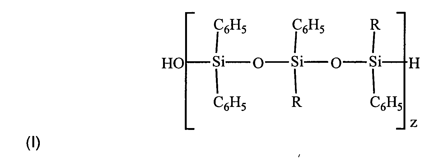
- In some embodiments silicone resins comprise the silicon resin of structure (I) where z is typically in a range between about 1 and about 10, and more typically, in a range between about 2 and about 5; R is selected from hydroxyl, C1-22 alkyl, C1-22 alkoxy, C2-22 alkenyl, C6-14 aryl, C6-22 alkyl-substituted aryl, and C6-22 aralkyl. Additionally, the silicone resin can be a branched structure in which R may be an OSiR3 substituent, where R3 can be hydroxyl, C1-22 alkyl, C1-22 alkoxy, C2-22 alkenyl, C6-14 aryl, C6-22 alkyl-substituted aryl, and C6-22 aralkyl.
- Epoxy resins (B) useful in the encapsulant of present invention include those described in "Chemistry and Technology of the Epoxy Resins," B. Ellis (Ed.) Chapman Hall 1993, New York and "Epoxy Resins Chemistry and Technology," C. May and Y. Tanaka, Marcell Dekker 1972, New York. Epoxy resins that can be used for the present invention include those that could be produced by reacting a hydroxyl, carboxyl, or amine-containing compound with epichlorohydrin, preferably in the presence of a basic catalyst such as a metal hydroxide, for example, sodium hydroxide. Also included are epoxy resins produced by reaction of a compound containing at least one and preferably two or more carbon-carbon double bond with a peroxide, for example, a peroxyacid. Examples of epoxy resins useful in the present invention include aliphatic epoxy resins, cycloaliphatic epoxy resins, bisphenol-A epoxy resins, bisphenol-F epoxy resins, phenol novolac epoxy resins, cresol-novolac epoxy resins, biphenyl epoxy resins, biphenyl epoxy resins, 4,4'-biphenyl epoxy resins, polyfunctional epoxy resins, divinylbenzene dioxide, and 2-glycidylphenylglycidyl ether. These epoxy resins can be used singly or in a combination of at least two epoxy resins. Preferred epoxy resins for the present invention are cycloaliphatic epoxy resins and aliphatic epoxy resins. Aliphatic epoxy resins include compounds that contain at least one aliphatic group and at least one epoxy group. Examples of aliphatic epoxies include, butadiene dioxide, dimethylpentane dioxide, diglycidyl ether, 1,4-butanedioldiglycidyl ether, diethylene glycol diglycidyl ether, and dipentene dioxide.
- Cycloaliphatic epoxy resins are compounds that contain at least about one cycloaliphatic group and at least one oxirane group. For example, cycloalipahtic epoxies may contain one cycloaliphatic group and at least two oxirane rings per molecule. Specific examples include 2-(3,4-epoxy)cyclohexyl-5, 5-spiro-(3,4-epoxy)cyclohexane-m-dioxane,3,4-epoxycyclohexylalkyl-3,4-epoxycyclohexanecarboxylate, 3,4-epoxy-6-methylcyclohexylmethyl-3,4-epoxy-6-methylcyclohexanecarboxylate, vinyl cyclohexanedioxide, bis(3,4-epoxycyclohexylmethyl)adipate, bis(3,4-epoxy-6-methylcyclohexylmethyl)adipate, exo-exo bis(2,3-epoxycyclopentyl) ether, endo-exo bis(2,3-epoxycyclopentyl) ether, 2,2-bis(4-(2,3-epoxypropoxy)cyclohexyl)propane, 2,6-bis(2,3-epoxypropoxycyclohexyl-p-dioxane), 2,6-bis(2,3-epoxypropoxy)norbonene, the diglycidylether of linoleic acid dimer, limonene dioxide, 2,2-bis(3,4-epoxycyclohexyl)propane, dicyclopentadiene dioxide, 1,2-epoxy-6-(2,3-epoxypropoxy)hexahydro-4,7-methanoindane, p-(2,3-epoxy)cyclopentylphenyl-2,3-epoxypropylether,1-(2,3-epoxypropoxy)phenyl-5,6-epoxyhexahydro-4,7-methanoindane, o-(2,3-epoxy)cyclopentylphenyl-2,3-epoxypropyl ether), 1,2-bis[5-(1,2-epoxy)-4,7-hexahydromethanoindanoxyl]ethane, cyclopentenylphenyl glycidyl ether, cyclohexanediol diglycidyl ether, and diglycidyl hexahydrophthalate.
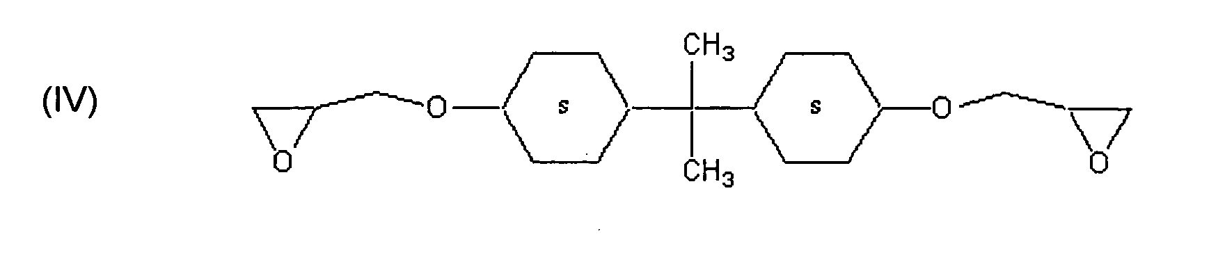
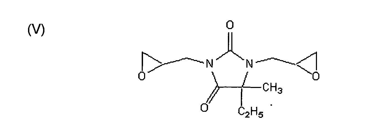
- Additional exemplary epoxy resins (B) of the present invention include those of structure (II), (III), (IV), and (V) given below.
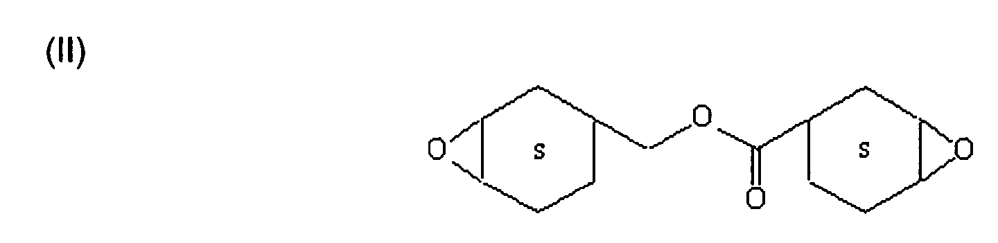
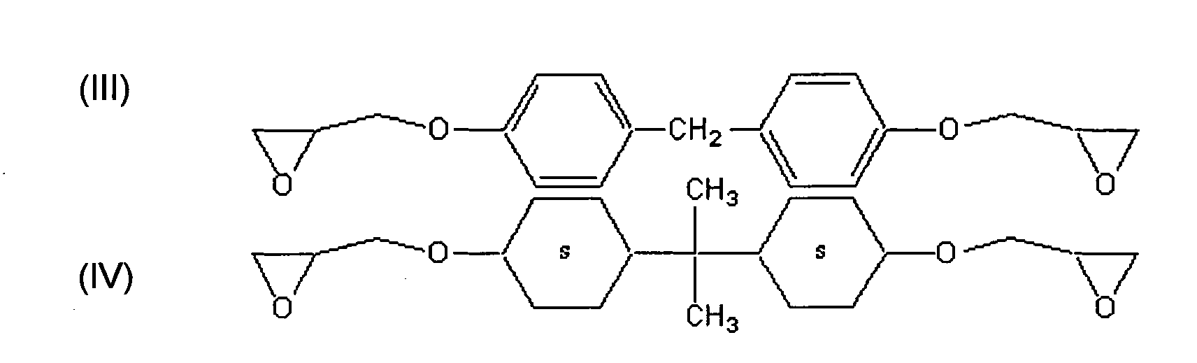
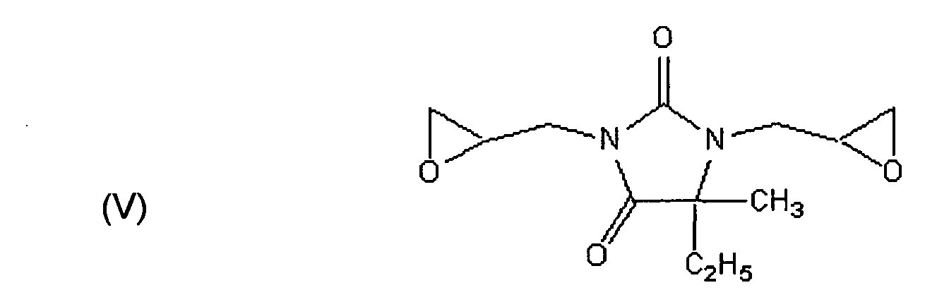
- Additives such as thermal stabilizers or antioxidants maybe used with aromatic epoxy resins to lessen discoloring. Flexibilizers are useful in the composition to reduce brittleness and include aliphatic epoxy resins, siloxane resins, and the like.
- Exemplary anhydride curing agents useful as component (C) typically include those of structures (VI) and (VII) below
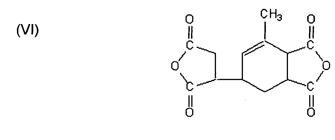 and bicyclo[2.2.1]hept-5-ene-2,3-dicarboxylic anhydride, methylbicyclo[2.2.1]hept-5-ene-2,3-dicarboxylic anhydride, bicyclo[2.2.1]hept-5-ene-2,3-dicarboxylic anhydride, phthalic anhydride, pyromellitic dianhydride, hexahydrophthalic anhydride, hexahydro-4-methylphthalic anhydride, dodecenylsuccinic anhydride, dichloromaleic anhydride, chlorendic anhydride, tetrachlorophthalic anhydride, and the like. Mixtures comprising at least two anhydride curing agents may also be used. Illustrative examples are described in "Chemistry and Technology of the Epoxy Resins" B. Ellis (Ed.) Chapman Hall, New York, 1993 and in "Epoxy Resins Chemistry and Technology", edited by C. A. May, Marcel Dekker, New York, 2nd edition, 1988.
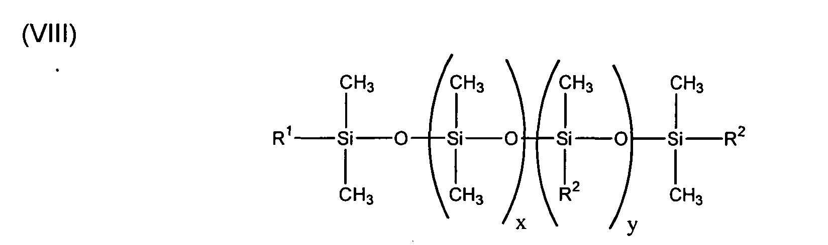
- The inventors have found that by using siloxane surfactants (D) it is possible to blend various components in the encapsulating composition resulting in homogeneity, clarity, low scattering properties, moisture resistance, and flexibility in addition to making the composition shatter proof. Siloxane surfactants are used to compatibilize the various materials used in the present invention. Siloxane surfactants may be used to compatibilize incompatible material into one homogeneous phase (i.e. uniform phase) by a reduction of interfacial tension to give desirable and required properties. For example, the silicone resin may be compatibilized with the epoxy resin using the siloxane surfactant. The siloxane surfactants used in the present invention may be functionalized with polyethylene glycol, polypropylene glycol, polypropylene glycol ethers and substituted siloxane polymers. The surfactants may be used singly or in combination thereof. The siloxane surfactants of the present invention may be used to compatibilize the silicone resin with the epoxy resin, curing agents, and optional refractive index modifiers and thermal stabilizers into one homogeneous composition which, when cured may give an encapsulant composition which may be clear and transparent with moisture resistance, solvent resistance, crack resistance properties, heat resistance, as well as UV absorption and light transmission in given wavelength ranges. The siloxane surfactant used in the present invention may be of the general structure (VIII)wherein R1 and R2 are independently at each occurrence selected from ethylene oxide, propylene oxide and methylene. In one embodiment of the present invention, R1 may be ethylene oxide while R2 may be a methyl group. In another embodiment, R1 may be a methyl group while R2 may be an ethylene oxide group. In a third embodiment, R1 may be a methyl group while R2 may be a mixture of ethylene oxide and propylene oxide groups. The values of x and y in structure (VIII) may be in a range between about 0 and about 20 in one embodiment while it may be in a range between about 3 to about 15 in another embodiment of the present invention. In a third embodiment of the present invention, the values of x and y in structure (VIII) may be in a range between about 5 to about 10. The percentage of silicon in the surfactant typically may be in a range between about 10% by weight and about 80% by weight of the total weight of the siloxane surfactant in one embodiment of the present invention, while it may be in a range between about 20% by weight and about 60% by weight of the total weight of the siloxane surfactant in a second embodiment of the invention. In a third embodiment, the silicon content may be in a range between about 25% and about 50% by weight of the total weight of the siloxane surfactant. The siloxane surfactant used in the present invention may have viscosities in a range between about 10 centistokes (cst) and about 2000 centistokes (cst) in one embodiment while it may have viscosities in a range between about 100 cst and about 1000 cst in a second embodiment and in a range between about 300 cst and about 600 cst in a third embodiment of the present invention. When present, the molecular weight of the polyether in the siloxane surfactant is typically in a range between about 100 and about 2000 in one embodiment of the present invention while it may be in a range between about 200 and about 1500 in a second embodiment and in a range between about 500 and about 1000 in a third embodiment of the present invention. In another embodiment, a siloxane surfactant that may be used in compatibilizing the silicone resin and the epoxy resin is given in structure (IX) given below.
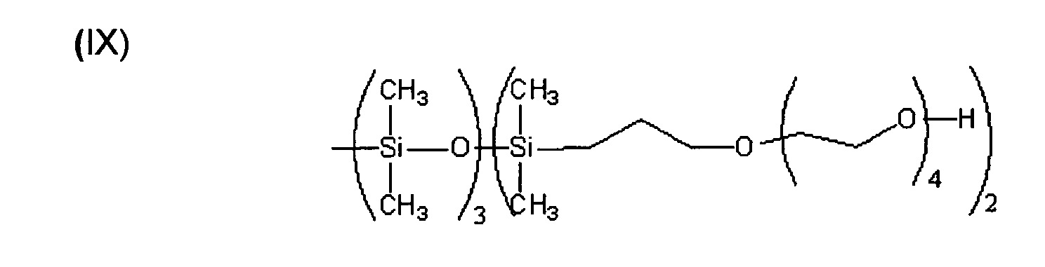
- Illustrative examples of ancillary curing catalysts (E) are described in "Chemistry and Technology of the Epoxy Resins" edited by B. Ellis, Chapman Hall, New York, 1993, and in "Epoxy Resins Chemistry and Technology", edited by C. A. May, Marcel Dekker, New York, 2nd edition, 1988. In various embodiments, the ancillary curing catalyst comprises an organometallic salt, a sulfonium salt or an iodonium salt. In particular embodiments, the ancillary curing catalyst comprises at least one of a metal carboxylate, a metal acetylacetonate, zinc octoate, stannous octoate, triarylsulfonium hexafluorophosphate, triarylsulfonium hexafluoroantimonate (such as CD 1010 sold by Sartomer Corporation), diaryliodonium hexafluoroantimonate, or diaryliodonium tetrakis(pentafluorophenyl)borate. These compounds can be used singly or in a combination of at least two compounds.
- The amounts of silicone resin (A), epoxy resin (B), anhydride curing agent (C), siloxane surfactant (D), and ancillary curing catalyst (E) can be varied over a wide range. In various embodiments, the amount of silicone resin (A) in the composition is greater than about 40% by weight based on the combined weight of the silicone resin (A), epoxy resin (B), anhydride curing gent (C), siloxane surfactant (D), and ancillary curing catalyst (E). In some embodiments, the amount of silicone resin (A) in the composition is in a range of between about 40% by weight and about 99% by weight based on the combined weight of silicone resin (A), epoxy resin (B), anhydride curing agent (C), siloxane surfactant (D), and ancillary curing catalyst (E). In other embodiments, the amount of silicone resin (A) in the composition is in a range of between about 76% by weight and about 99% by weight based on the combined weight of silicone resin (A), epoxy resin (B), anhydride curing agent (C), siloxane surfactant (D), and ancillary curing catalyst (E). When the silicone resin, epoxy resin, the siloxane surfactant, the anhydride curing agent, and the ancillary curing catalyst are mixed in to give an encapsulating composition and the composition is cured and polished, the resulting surface may be transparent and clear and the encapsulant material may be crack-proof and may not scatter light.
- In various embodiments of the present invention, the amount of anhydride curing agent (C), in the composition is less than about 40% by weight based on the combined weight of silicone resin (A), epoxy resin (B), anhydride curing agent (C), siloxane surfactant (D), and ancillary curing catalyst (E). In other embodiments, the amount of curing agent (C) in the composition is less than about 25% by weight based on the combined weight of silicone resin (A), epoxy resin (B), anhydride curing agent (C), siloxane surfactant (D), and ancillary curing catalyst (E). In some embodiments, the amount of anhydride curing agent (C) in the composition is in a range of between about 1% by weight and about 24% by weight based on the combined weight of silicone resin (A), epoxy resin (B), anhydride curing agent (C) siloxane surfactant (D), and ancillary curing catalyst (E). In other embodiments, the amount of anhydride curing agent (C) in the composition is in a range of between about 1% by weight and about 20% by weight based on the combined weight of silicone resin (A), epoxy resin (B), anhydride curing agent (C), siloxane surfactant (D), and ancillary curing catalyst (E).
- In various embodiments, the amount of ancillary curing catalyst (E) in the composition is less than about 10% by weight based on the combined weight of silicone resin (A), epoxy resin (B), anhydride curing agent (C), siloxane surfactant (D) and ancillary curing catalyst (E). In some embodiments, the amount of ancillary curing catalyst (E) in the composition is in a range between about 0.008% by weight and about 10% by weight based on the combined weight of silicone resin (A), epoxy resin (B), anhydride curing agent (C), siloxane surfactant (D), and ancillary curing catalyst (E). In other embodiments, the amount of ancillary curing catalyst (E) in the composition is in a range between about 0.01 % by weight and about 5% by weight based on the combined weight of silicone resin (A), epoxy resin (B), anhydride curing agent (C), siloxane surfactant (D), and ancillary curing catalyst (E). In some embodiments the amount of ancillary curing catalyst (E) in the composition is in a range between about 0.01 % by weight and about 1.0 % by weight based on the combined weight of silicone resin (A), epoxy resin (B), anhydride curing agent (C), siloxane surfactant (D), and ancillary curing catalyst (E). In other embodiments the amount of ancillary curing catalyst (E) in the composition is in a range between about 0.01% by weight and about 0.5% by weight based on the combined weight of silicone resin (A), epoxy resin (B), anhydride curing agent (C), siloxane surfactant (D) and ancillary curing catalyst (E).
- One or more thermal stabilizers, UV-stabilizers or mixtures thereof may optionally be present in the compositions of the invention. Such stabilizers may reduce color formation during processing of the encapsulant. Examples of stabilizers are described in J. F. Rabek, "Photostabilization of Polymers; Principles and Applications", Elsevier Applied Science, NY, 1990 and in "Plastics Additives Handbook", 5th edition, edited by H. Zweifel, Hanser Publishers, 2001. Illustrative examples of suitable stabilizers comprise organic phosphites and phosphonites, such as triphenyl phosphite, diphenylalkyl phosphites, phenyldialkyl phosphites, tri-(nonylphenyl) phosphite, trilauryl phosphite, trioctadecyl phosphite, di-stearyl-pentaerythritol diphosphite, tris-(2,4-di-tert-butylphenyl) phosphite, di-isodecylpentaerythritol diphosphite, di-(2,4-di-tert-butylphenyl) pentaerythritol diphosphite, tristearylsorbitol triphosphite, and tetrakis-(2,4-di-tert-butylphenyl)-4,4'-biphenyldiphosphonite. Illustrative examples of suitable stabilizers also comprise sulfur-containing phosphorus compounds such as trismethylthiophosphite, trisethylthiophosphite, trispropylthiophosphite, trispentylthiophosphite, trishexylthiophosphite, trisheptylthiophosphite, trisoctylthiophosphite, trisnonylthiophosphite, trislaurylthiophosphite, trisphenylthiophosphite, trisbenzylthiophosphite, bispropiothiomethylphosphite, bispropiothiononylphosphite, bisnonylthiomethylphosphite, bisnonylthiobutylphosphite, methylethylthiobutylphosphite, methylethylthiopropiophosphite, methylnonylthiobutylphosphite, methylnonylthiolaurylphosphite, and pentylnonylthiolaurylphosphite. These compounds can be used singly or in a combination of at least two compounds.
- Suitable stabilizers also comprise sterically hindered phenols. Illustrative examples of sterically hindered phenol stabilizers comprise 2-tertiary-alkyl-substituted phenol derivatives, 2-tertiary-amyl-substituted phenol derivatives, 2-tertiary-octyl-substituted phenol derivatives, 2-tertiary-butyl-substituted phenol derivatives, 2,6-di-tertiary-butyl-substituted phenol derivatives, 2-tertiary-butyl-6-methyl- (or 6-methylene-) substituted phenol derivatives, and 2,6-di-methyl-substituted phenol derivatives. These compounds can be used singly or in a combination of at least two compounds. In certain particular embodiments of the present invention, sterically hindered phenol stabilizers comprise alpha-tocopherol and butylated hydroxy toluene.
- Suitable stabilizers also comprise sterically hindered amines, illustrative examples of which comprise bis-(2,2,6,6-tetramethylpiperidyl) sebacate, bis-(1,2,2,6,6-pentamethylpiperidyl) sebacate, n-butyl-3,5-di-tert-butyl-4-hydroxybenzyl malonic acid bis-(1,2,2,6,6-pentamethylpiperidyl)ester, condensation product of 1-hydroxyethyl-2,2,6,6-tetramethyl-4-hydroxypiperidine and succinic acid, condensation product of N,N'-(2,2,6,6-tetramethylpiperidyl)-hexamethylenediamine and 4-tert-octyl-amino-2,6-dichloro-s-triazine, tris-(2,2,6,6-tetramethylpiperidyl)-nitrilotriacetate, tetrakis-(2,2,6,6-tetramethyl-4-piperidyl)-1,2,3,4-butanetetracarboxylate, and 1,1'-(1,2-ethanediyl)-bis-(3,3,5,5-tetramethylpiperazinone). These compounds can be used singly or in a combination of at least two compounds.
- Suitable stabilizers also comprise compounds which destroy peroxide, illustrative examples of which comprise esters of beta-thiodipropionic acid, for example the lauryl, stearyl, myristyl or tridecyl esters; mercaptobenzimidazole or the zinc salt of 2-mercaptobenzimidazole; zinc dibutyl-dithiocarbamate; dioctadecyl disulfide; and pentaerythritol tetrakis-(beta-dodecylmercapto)-propionate. These compounds can be used singly or in a combination of at least two compounds.
- Optional components in the present invention also comprise cure modifiers which may modify the rate of cure of epoxy resin. In various embodiments of the present invention, cure modifiers comprise at least one cure accelerators or cure inhibitors. Cure modifiers may comprise compounds containing heteroatoms that possess lone electron pairs. Phosphites may be used as cure modifiers. Illustrative examples of phosphites comprise trialkylphosphites, triarylphosphites, trialkylthiophosphites, and triarylthiophosphites. In some embodiments of the present invention, phosphites comprise triphenyl phosphite, benzyldiethyl phosphite, or tributyl phosphite. Other suitable cure modifiers comprise sterically hindered amines and 2,2,6,6-tetramethylpiperidyl residues, such as for example bis(2,2,6,6-tetramethylpiperidyl) sebacate. Mixtures of cure modifiers may also be employed.
- Optional components in the present invention also comprise coupling agents which in various embodiments may help epoxy resin bind to a matrix, such as a glass matrix, so as to form a strong bond to the surface such that premature failure does not occur. Coupling agents comprise compounds that contain both silane and mercapto moieties, illustrative examples of which comprise mercaptomethyltriphenylsilane, beta-mercaptoethyltriphenylsilane, beta-mercaptopropyltriphenylsilane, gamma-mercaptopropyldiphenylmethylsilane, gamma-mercaptopropylphenyldimethylsilane, delta-mercaptobutylphenyldimethylsilane, delta-mercaptobutyltriphenylsilane, tris(beta-mercaptoethyl) phenylsilane, tris(gamma-mercaptopropyl)phenylsilane, tris(gamma-mercaptopropyl)methylsilane, tris(gamma-mercaptopropyl)ethylsilane, and tris(gamma-mercaptopropyl)benzylsilane. Coupling agents also comprise compounds which comprise both an alkoxysilane and an organic moiety, illustrative examples of which comprise compounds of the formula (R5O)3Si-R6 wherein R5 is an alkyl group and R6 is selected from the group consisting of vinyl, 3-glycidoxypropyl, 3-mercaptopropyl, 3-acryloxypropyl, 3-methacryloxypropyl, and CnH2n+1 wherein n has a value in a range between about 4 and about 16.
- In some embodiments of the present invention, R5 is methyl or ethyl. In other embodiments of the present invention, coupling agents comprise compounds that contain both an alkoxysilane and an epoxy moiety. Coupling agents can be used singly or in a combination of at least two compounds.
- Optional components in the present invention also comprise refractive index modifiers. As light passes from the relatively high index of diffraction chip (typically in a range between about 2.8 and 3.2) to the lower refractive index epoxy encapsulant (typically in a range between about 1.2 and about 1.6) some of the light is reflected back to the chip at the critical angle. Modifiers with high refractive index added to the epoxy increase its refractive index, producing a better match of the two refractive indices and an increase in the amount of emitted light. Such materials increase the refractive index of the epoxy without significantly affecting the transparency of the epoxy encapsulant. Modifiers of this type comprise additives with high refractive index. These materials comprise optically transparent organics or inorganics such as silicone fluids, and agglomerates of particles or structures whose size is less than the size of the wavelength of the emitted light. Such agglomerates are sometimes referred to as nanoparticles. Examples of agglomerates comprise a variety of transparent metal oxides or Group II-VI materials that are relatively free from scattering. In one embodiment, a nanoparticle material is titanium dioxide. In other embodiments, other types of transparent metal oxides or combinations of metal oxides can be used. For example, magnesium oxide, yttria, zirconia, cerium oxides, alumina, lead oxides, and composite materials such as those comprising yttria and zirconia can be used to produce nanoparticles. In other embodiments, nanoparticles are made from one of the Group II-VI materials comprising zinc selenide, zinc sulphide, and alloys made from Zn, Se, S, and Te. Alternatively, gallium nitride, silicon nitride, or aluminum nitride can be also used to make nanoparticles. Refractive index modifiers can be used singly or in a combination of at least two compounds. In one embodiment of the present invention, the refractive index of the encapsulating composition is in a range between about 0.1 and about 10.0. In a second embodiment, the refractive index is in a range between about 0.5 and about 5.0 and in a third embodiment, the refractive index is in a range between about 1.0 and about 2.5. In many embodiments, the refractive index is in a range between about 1.0 and about 2.0.
- The compositions of the present invention can be prepared by combining the various components, including optional components, in any convenient order. In various embodiments, all the components may be mixed together. In other embodiments, two or more components may be premixed and then subsequently combined with other components. In one embodiment, the components of the compositions of the present invention comprise a two-part composition, wherein the various components are premixed in at least two separate compositions before combination to provide a final composition.
- Encapsulation techniques for solid-state devices comprise casting, resin transfer molding and the like. After the solid-state device is enveloped in the uncured resin, typically performed in a mold, the resin is cured. These resins may be cured in one or more stages using methods such as thermal, UV, electron beam techniques, or combinations thereof. For example, thermal cure may be performed at temperatures in one embodiment in a range of between 20°C and about 200°C, in another embodiment in a range between about 80°C and about 200°C, in another embodiment in a range between about 100°C and about 200°C, and in another embodiment in a range between about 120°C and about 160°C. Also in other embodiments these materials can be photo-chemically cured, initially at about room temperature. Although some thermal excursion from the photochemical reaction and subsequent cure can occur, no external heating is typically required. In other embodiments, these materials may be cured in two stages wherein an initial thermal or UV cure, for example, may be used to produce a partially hardened or B-staged epoxy resin. This material, which is easily handled, may then be further cured using, for example, either thermal or UV techniques, to produce a material with the desired thermal performance (for example glass transition temperature (Tg) and coefficient of thermal expansion (CTE)), optical properties and moisture resistance required for encapsulated solid state devices.
- When the silicone resin (A), the epoxy resin (B), the siloxane surfactant (D), the anhydride curing agent (C) and the ancillary curing catalyst (E) are mixed and cured to give the encapsulating material, the coefficient of thermal expansion measured above the glass transition temperature varies in a range between about 10 and about 100 in one embodiment of the present invention, in a range between about 50 and about 90 in a second embodiment of the present invention, and in a range between about 60 and about 85 in a third embodiment of the present invention. The coefficient of thermal expansion when measured below the glass transition temperature varies in a range between about 50 and about 300 in one embodiment of the present invention while in a second embodiment the coefficient of thermal expansion varies in a range between about 100 and about 275 and in a third embodiment the coefficient of thermal expansion varies in a range between about 150 and about 250.
- The silicone resin (A), the epoxy resin (B), the siloxane surfactant (D), the anhydride curing agent (C), and the ancillary curing catalyst (E) when mixed into an encapsulating composition may give desirable glass transition values. In one embodiment the glass transition temperature of the composition is in a range between about 10°C and about 250°C while in a second embodiment the glass transition is in a range between about 20°C and about 200°C. In a third embodiment, the glass transition of the encapsulating composition varies in a range between about 24°C and about 150°C.
- The epoxy resin compositions of the present invention can be used in applications known for epoxy resin compositions. Such applications comprise coatings, potting compounds, and encapsulants for solid-state devices. In one embodiment, a solid-state device is a
LED 1. Figure 1 schematically illustrates aLED 1 according to one embodiment of the present invention. TheLED 1 contains aLED chip 4, which is electrically connected to alead frame 5. For example, theLED chip 4 may be directly electrically connected to an anode or cathode electrode of thelead frame 5 and connected by alead 7 to the opposite cathode or anode electrode of thelead frame 5, as illustrated in Figure 1. In a particular embodiment illustrated in Figure 1, thelead frame 5 supports theLED chip 4. However, thelead 7 may be omitted, and theLED chip 4 may straddle both electrodes of thelead frame 5 with the bottom of theLED chip 4 containing the contact layers, which contact both the anode and cathode electrode of thelead frame 5. Thelead frame 5 connects to a power supply, such as a current or voltage source or to another circuit (not shown). - The
LED chip 4 emits radiation from theradiation emitting surface 9. TheLED 1 may emit visible, ultraviolet or infrared radiation. TheLED chip 4 may comprise anyLED chip 4 containing a p-n junction of any semiconductor layers capable of emitting the desired radiation. For example, theLED chip 4 may contain any desired Group III-V compound semiconductor layers, such as GaAs, GaAlAs, GaN, InGaN, GaP, etc., or Group II-VI compound semiconductor layers such ZnSe, ZnSSe, CdTe, etc., or Group IV-IV semiconductor layers, such as SiC. TheLED chip 4 may also contain other layers, such as cladding layers, waveguide layers and contact layers. - The
LED 1 is packaged with anencapsulant 11 of the present invention. An alternative term for encapsulant is encapsulating material. In one embodiment, the LED packaging includesencapsulant 11 located in a package, such as ashell 14. Theshell 14 may be any plastic or other material, such as polycarbonate, which is transparent to the LED radiation. However, theshell 14 may be omitted to simplify processing ifencapsulant 11 has sufficient toughness and rigidity to be used without ashell 14. Thus, the outer surface ofencapsulant 11 would act in some embodiments as ashell 14 or package. Theshell 14 contains a light orradiation emitting surface 15 above theLED chip 4 and anon-emitting surface 16 adjacent to thelead frame 5. Theradiation emitting surface 15 may be curved to act as a lens and/or may be colored to act as a filter. In various embodiments thenon-emitting surface 16 may be opaque to the LED radiation, and may be made of opaque materials such as metal. Theshell 14 may also contain a reflector around theLED chip 4, or other components, such as resistors, etc., if desired. - In other embodiments, encapsulating materials may optionally contain a phosphor to optimize the color output of the
LED 1. For example, a phosphor may be interspersed or mixed as a phosphor powder withencapsulant 11 or coated as a thin film on theLED chip 4 or coated on the inner surface of theshell 14. Any phosphor material may be used with the LED chip. For example, a yellow emitting cerium doped yttrium aluminum garnet phosphor (YAG:Ce3+) may be used with a blue emitting InGaN active layer LED chip to produce a visible yellow and blue light output which appears white to a human observer. Other combinations of LED chips and phosphors may be used as desired. - While the packaged
LED chip 4 is supported by thelead frame 5 according to one embodiment as illustrated in Figure 1, theLED 1 can have various other structures. For example, theLED chip 4 may be supported by thebottom surface 16 of theshell 14 or by a pedestal (not shown) located on the bottom of theshell 14 instead of by thelead frame 5. - In another embodiment of the present invention, the encapsulating composition may be used with a vertical cavity surface emitting laser (VCSEL). A schematic diagram of the device is shown in Figure 2. The
VCSEL 30 may be embedded inside apocket 32 of a printedcircuit board assembly 33. Aheat sink 34 maybe placed in thepocket 32 of the printedcircuit board 33 and theVCSEL 30 may rest on theheat sink 34. Theencapsulant composition 36 of the invention may be injected into thecavity 35 of thepocket 32 in the printedcircuit board 33 and may flow around the VCSEL and encapsulate it on all sides and also form acoating top film 36 on the surface of theVCSEL 30. Thetop coating film 36 protects theVCSEL 30 from damage and degradation and at the same time is inert to moisture and is transparent and polishable. Thelaser beams 37 emitting from the VCSEL may strike themirrors 38 to be reflected out of thepocket 32 of the printedcircuit board 33. - In another embodiment of the present invention, a
LED array 3 may be fabricated on a plastic substrate, as illustrated in Figure 3. The LED chips or die 4 are physically and electrically mounted on cathode leads 26. The top surfaces of theLED chips 4 are electrically connected to anode leads 25 withlead wires 27. The lead wires may be attached by known wire bonding techniques to a conductive chip pad. The leads 26, 25 comprise a lead frame and may be made of a metal, such as silver plated copper. The lead frame andLED chip array 3 are contained in aplastic package 29, such as, for example, a polycarbonate package, a polyvinyl chloride package or a polyetherimide package. In some embodiments the polycarbonate comprises a bisphenol A polycarbonate. Theplastic package 29 is filled with anencapsulant 11 of the present invention. Thepackage 29 contains taperedinterior sidewalls 18, which enclose theLED chips 4, and form a light spreadingcavity 20, which ensures cross fluxing of LED light. - Without further elaboration, it is believed that one skilled in the art can, using the description herein, utilize the present invention to its fullest extent. The following examples are included to provide additional guidance to those skilled in the art in practicing the claimed invention. The examples provided are merely representative of the work that contributes to the teaching of the present application. Accordingly, these examples are not intended to limit the invention, as defined in the appended claims, in any manner.
- The following procedure was used to make
Sample 1 shown in Table 1. Into a small jar was placed 11.4 grams Z6018, (phenyl propyl hydroxy silicone from Dow Chemicals), 7.5 grams hexahydro-phthalic-anhydride (HHPA) (Ciba Geigy) and 0.4 grams SF1488 (polydimethylsiloxane surfactant from General Electric Co.). A cap was placed onto the jar and the contents heated using a microwave oven to a temperature of approximately 80°C and mixed until all components were completely dissolved. After dissolution was complete, the sample was cooled to below 50°C, and 15 grams CY179, (cycloaliphatic epoxy resin from Ciba Geigy), 0.1 grams Irganox 1010 (antioxidant from Ciba) and 0.3 grams Tin ethyl-hexanoate were added. The material was blended and filtered through a nominal 5 micron pore sized filter into a clean jar. After filtration, the epoxy blend was degassed by placing it in a vacuum oven set at less than 60°C for approximately 30 minutes while vacuum was applied. Once degassed the material was used to encapsulate components. A sample disk of the material was prepared by pouring the blend into an aluminum dish, covering it and curing the epoxy for 1 hour at 80°C, ramping to 180°C over 1 hour, and holding at temperature for 2 hours. Other epoxy resin encapsulants were prepared using the procedure forSample 1 by combining the various epoxy and silicone comprising resins, curing agents and other components and curing under the specified conditions as shown in Table 1. All quantities are in grams. While samples 1-3 were vacuum degassed and cured for 1 hour at 140°C giving clear hard and transparent samples,samples Sample 8 was degassed for 2 hours at 175-180°C to give a clear light orange sample. All samples were polishable and did not crack due to shock.Epoxy cure studies Sample 1Sample 2 Sample 3Sample 4Sample 5Sample 6Sample 7Sample 8CY 179 15.00 5.00 21.00 Epon 862, Bis F Epoxy 10.00 Shell Eponex 1510 24.00 10.75 Araldite AY 238 7.60 Silikoftal ED 5.10 10.80 5.50 5.00 10.80 Z6018 11.40 5.60 5.09 4.50 5.00 14.60 13.00 HHPA 7.50 4.50 2.09 6.60 6.00 14.40 10.00 11.00 Epicuron B-4400 dianhydride 3.00 Sn Octoate 0.30 0.20 0.11 0.27 0.25 0.60 0.20 Ciba Irganox1010 0.10 0.10 0.10 0.11 0.13 0.29 0.10 0.15 SF 1488 0.40 0.30 0.25 0.55 0.50 0.70 0.27 0.5 Final sample thickness/mi Is 158 161 143 230 253 258 275 258 Silicone component % 33 52 88 40 38 27 34 27 Tg/°C 140 87 24 92 64 64 55 148 - Encapsulant compositions used in the invention are shown in Table-2.
Component, %wt Material type One component % HHPA B-4400 Optional items Surfactant CY 179 Epoxy 0-50 % Epon 882 BisF Epoxy Epoxy 0-50 % Shell Eponex1510 Epoxy 0-50 % Araldite AY 238 Epoxy 0-50 % Silkoftal EDZ6018 Silicone epoxy 0-70 % HHPA Anhydride Hardener 5-50 % Epiclon B 4400 Dianhydride Anhydride hardener 0-10% Sn Octoate Accelaration catlyst 0.5 % Ciba Irganox 1010 Antioxidant 0-5 SF 1488 Silicone surfactant 0.5-1 Ciba Tinuvin UV absorber 0-5 Z 6018 Silicone resin 1-50 - UV-Vis-Near IR Transmission spectrum for silicone containing epoxy blends with siloxane surfactants is shown in Figure 4 for compositions described in Tables 1 and 2. The spectra indicate transmission in a range between about 500 nm and about 1100nm.
- Figure 5 shows UV-Vis absorption spectra for silicone containing epoxy blends. (The compositions are given in Tables 1 and 2.) No absorptions are seen beyond 500nm.
- Refractive index against wavelength data for silicone epoxy blends is shown in Fig. 6 for compositions given in Tables 1 and 2. Refractive index values decreased from 1.58 at 350 nm to about 1.49 at 1700nm.
- For the sake of good order, various aspects of the invention are set out in the following clauses:-
- 1. A curable epoxy resin composition for encapsulation of a solid state device, which comprises (A) at least one silicone resin, (B) at least one epoxy resin, (C) at least one anhydride curing agent, (D) at least one siloxane surfactant, and (E) at least one ancillary curing catalyst.
- 2. The composition of
clause 1, wherein the silicone resin comprises a silicone resin of structure (I)wherein R is independently at each occurrence a hydroxyl group, C1-22 alkyl, C1-22 alkoxy, C2-22 alkenyl, C6-14 aryl, C6-22 alkyl-substituted aryl, C6-22 aralkyl, or OSiR3 wherein R3 is independently at each occurrence hydroxyl, C1-22 alkyl, C1-22 alkoxy, C2-22 alkenyl, C6-14 aryl, C6-22 alkyl-substituted aryl, or C6-22 aralkyl; and wherein z is in a range between about 1 and about 10.
- 3. The composition of
clause 1, wherein the epoxy resin is selected from the group consisting of aliphatic epoxy resins, cycloaliphatic epoxy resins, bisphenol-A epoxy resins, bisphenol-F epoxy resins, phenol novolac epoxy resins, cresol-novolac epoxy resins, biphenyl epoxy resins, biphenyl epoxy resins, 4,4'-biphenyl epoxy resins, polyfunctional epoxy resins, divinylbenzene dioxide, 2-glycidylphenylglycidyl ether, and combinations thereof. - 4. The composition of
clause 1, wherein the epoxy resin is selected from the group consisting of epoxy resins in structures (II) to (V)
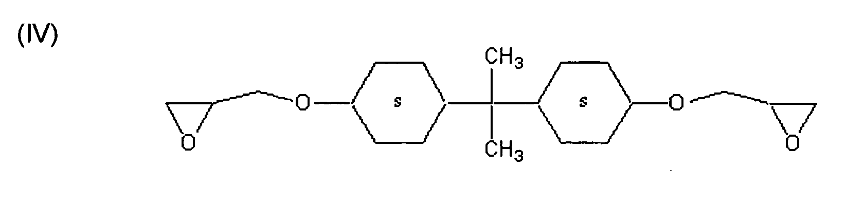
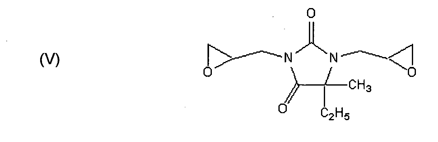
- 5. The composition of
clause 1, wherein the anhydride curing agent is selected from the group consisting of bicyclo[2.2.1 ]hept-5-ene-2,3-dicarboxylic anhydride, methylbicyclo[2.2.1]hept-5-ene-2,3-dicarboxylic anhydride, bicyclo[2.2.1]hept-5-ene-2,3-dicarboxylic anhydride, phthalic anhydride, pyromellitic dianhydride, hexahydrophthalic anhydride, hexahydro-4-methylphthalic anhydride, dodecenylsuccinic anhydride, dichloromaleic anhydride, chlorendic anhydride, tetrachlorophthalic anhydride, and combinations thereof. - 6. The composition of
clause 1, wherein the anhydride curing agent is a compound of structure (VI), (VII), or combination thereof
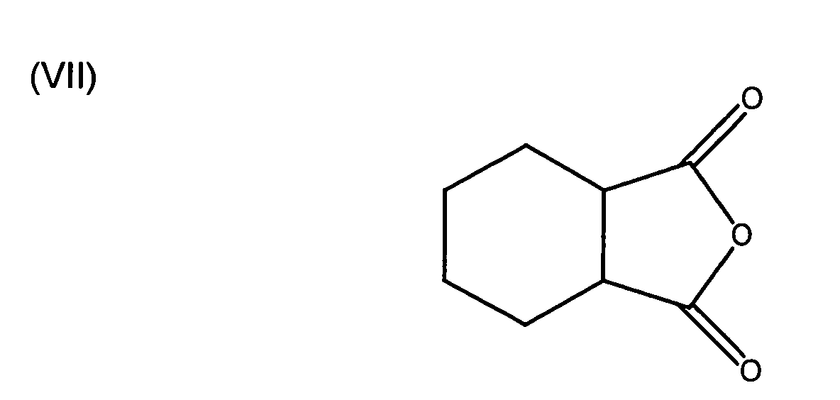
- 7. The composition of
clause 1 wherein the siloxane surfactant is a compound of structure (VIII), (IX), or combination thereof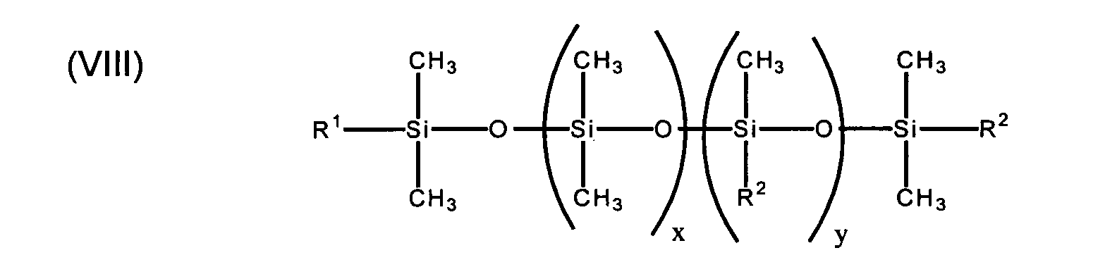 wherein R1 and R2 are independently at each occurrence selected from ethylene oxide, propylene oxide and methylene in structure (VIII) and where x and y are in a range between 0 and about 20 in structure (VIII).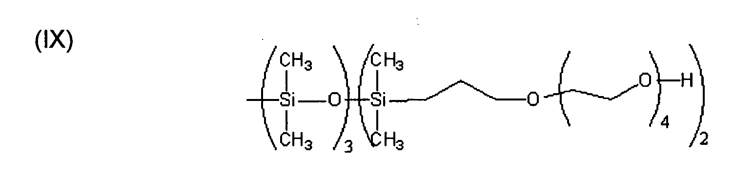
- 8. The composition of
clause 1, wherein the anhydride curing agent (C) comprises hexahydro-4-methylphthalic anhydride. - 9. The composition of
clause 1 further comprising refractive index modifiers selected from the group consisting of magnesium oxide, yttria, zirconia, cerium oxides, alumina, lead oxides, zinc selenide, zinc sulphides, alloys made from Zn, Se, S, and Te, gallium nitride, silicon nitride, aluminum nitride, and combinations thereof. - 10. The composition of
clause 1, wherein the composition is cured in a range between about 100°C and about 200°C. - 11. The composition of
clause 1, wherein the ancillary curing catalyst (E) is selected from the group consisting of an organometallic salt, a sulfonium salt, an iodonium salt, and combinations thereof. - 12. The composition of
clause 1, wherein the ancillary curing catalyst (E) is selected from the group consisting of a metal carboxylate, a metal acetylacetonate, zinc octoate, stannous octoate, triarylsulfonium hexafluorophosphate, triarylsulfonium hexafluoroantimonate, diaryliodonium hexafluoroantimonate, diaryliodonium tetrakis(pentafluorophenyl)borate, and combinations thereof. - 13. The composition of
clause 1 further comprises zinc octoate. - 14. The composition of
clause 1, comprising at least one of a hindered phenol stabilizer, a phosphite stabilizer, or combinations thereof. - 15. The composition of
clause 1 wherein the refractive index of the composition is in a range between about 0.1 and about 10.0. - 16. The composition of
clause 1 wherein the composition is clear, transparent, polishable and crackfree. - 17. A curable epoxy resin composition for encapsulation of a solid state device, which comprises (A) a silicone resin comprising a hydroxyfunctional silicone resin, (B) an epoxy resin comprising bisphenol A epoxy resin, (C) an anhydride curing agent comprising hexahydro-4-methylphthalic anhydride, (D) a siloxane surfactant comprising ethylene oxide functionalized siloxane, and (E) an ancillary curing catalyst zinc octoate, wherein component (A) is present at a level of greater than about 40% by weight; component (B) is present at a level in a range of between about 1% by weight and about 20% by weight; component (C) is present at a level of less than about 40% by weight; and component (D) and (E) are present at a level in a range between about 0.008% by weight and about 10% by weight based on the combined weight of silicone resin (A), epoxy resin (B), anhydride curing agent (C), siloxane surfactant (D) and ancillary curing catalyst (E).
- 18. The composition of clause 17 further comprising at least one of a thermal stabilizer, a UV stabilizer, or combinations thereof.
- 19. The composition of clause 17 wherein the composition has a glass transition temperature varying in a range between about 24°C and about 150°C.
- 20. The composition of clause 17 wherein the composition has a refractive index in a range between about 0.1 and about 10.0.
- 21. A packaged solid state device comprising: (a) a package; (b) a chip (4); and (c) an encapsulant (11) comprising: (A) at least one silicone resin, (B) at least one epoxy resin, (C) at least one anhydride curing agent, (D) at least one siloxane surfactant, and (E) at least one ancillary curing catalyst.
- 22. The packaged solid state device of clause 21, wherein the solid state device is a semiconductor device.
- 23. The packaged solid state device of clause 21, wherein the solid state device is an opto-electronic device.
- 24. The packaged solid state device of clause 21, wherein the opto-electronic device is semiconductor device comprising: a LED (1), CCD, LSI, photodiode, phototransistor, or opto-electronic coupler.
- 25. The packaged solid state device of clause 21, wherein the package comprises a shell (14) or lens.
- 26. The packaged solid state device of clause 21, wherein the silicone
resin comprises a silicone resin selected from the silicone resin in structure (I)
wherein R is independently at each occurrence a hydroxyl group, C1-22 alkyl, C1-22 alkoxy, C2-22 alkenyl, C6-14 aryl, C6-22 alkyl-substituted aryl, C6-22 aralkyl, or OSiR3 wherein R3 is independently at each occurrence hydroxyl, C1-22 alkyl, C1-22 alkoxy, C2-22 alkenyl, C6-14 aryl, C6-22 alkyl-substituted aryl, or C6-22 aralkyl; and wherein z is in a range between about 1 and about 10.

- 27. The packaged solid state device of clause 21, wherein the epoxy resin is selected from the group consisting of aliphatic epoxy resins, cycloaliphatic epoxy resins, bisphenol-A epoxy resins, bisphenol-F epoxy resins, phenol novolac epoxy resins, cresol-novolac epoxy resins, biphenyl epoxy resins, biphenyl epoxy resins, 4,4'-biphenyl epoxy resins, polyfunctional epoxy resins, divinylbenzene dioxide, 2-glycidylphenylglycidyl ether, and combinations thereof.
- 28. The packaged solid state device of clause 21, wherein the epoxy resin
is a resin selected from the structures (II) to (V)


- 29. The packaged solid state device of clause 21 wherein the anhydride curing agent is selected from the group consisting of bicyclo[2.2.1]hept-5-ene-2,3-dicarboxylic anhydride, methylbicyclo[2.2.1]hept-5-ene-2,3-dicarboxylic anhydride, bicyclo[2.2.1]hept-5-ene-2,3-dicarboxylic anhydride, phthalic anhydride, pyromellitic dianhydride, hexahydrophthalic anhydride, hexahydro-4-methylphthalic anhydride, dodecenylsuccinic anhydride, dichloromaleic anhydride, chlorendic anhydride, tetrachlorophthalic anhydride, and combinations thereof.
- 30. The packaged solid state device of clause 21, wherein the anhydride
curing agent (C) is a compound of structure (VI), (VII), or combination thereof
- 31. The packaged solid state device of clause 21 wherein the anhydride curing agent (C) comprises hexahydro-4-methylphthalic anhydride.
- 32. The packaged solid state device of clause 22 wherein the siloxane
surfactant is a compound of structure (VIII), (IX), or combination thereof
 wherein R1 and R2 are independently at each occurrence selected from methylene, ethylene oxide and propylene oxide in structure (VIII) and wherein x and y are in a range between 0 and about 20 in structure (VIII).
- 33. The packaged solid state device of clause 21, wherein the ancillary curing catalyst (E) is selected from the group consisting of an organometallic salt, a sulfonium salt, an iodonium salt, and combinations thereof.
- 34. The packaged solid state device of clause 21, wherein the ancillary curing catalyst (E) comprises at least one member selected from the group consisting of a metal carboxylate, a metal acetylacetonate, zinc octoate, stannous octoate, triarylsulfonium hexafluorophosphate, triarylsulfonium hexafluoroantimonate, diaryliodonium hexafluoroantimonate, diaryliodonium tetrakis(pentafluorophenyl)borate, and combinations thereof.
- 35. The packaged solid state device of clause 21, wherein the ancillary curing catalyst (E) is zinc octoate.
- 36. The packaged solid state device of clause 21, further comprising at least one of thermal stabilizers, UV stabilizers, cure modifiers, coupling agents, refractive index modifiers, or combinations thereof.
- 37. The packaged solid state device of clause 21, comprising at least one of a thermal stabilizer, a UV stabilizer, or combinations thereof.
- 38. The packaged solid state device of clause 21 wherein the encapsulant is clear, transparent, crackfree and polishable.
- 39. The packaged solid state device of clause 21 wherein the encapsulant (11) has a glass transition varying in a range between about 24°C and about 150°C.
- 40. The packaged solid state device of clause 21 wherein the encapsulant (11) has a refractive index in a range between about 0.1 and about 10.0.
- 41. A LED (1) device comprising: (a) a package; (b) a LED chip (4); and (c) an encapsulant (11) comprising: (A) a silicone resin comprising a hydroxyfunctional silicone resin, (B) an epoxy resin comprising a bisphenol F resin, (C) an anhydride curing agent comprising hexahydro-4-methylphthalic anhydride, (D) a siloxane surfactant comprising propylene oxide modified siloxane, and (E) a ancillary curing catalyst comprising zinc octoate, wherein component (A) is present at a level of greater than about 40% by weight; component (B) is present at a level in a range of between about 1% by weight and about 20% by weight; component (C) is present at a level of less than about 40% by weight; and component (D) and (E) are present at a level in a range between about 0.008% by weight and about 10% by weight based on the combined weight of silicone resin (A), epoxy resin (B), a siloxane surfactant (D) anhydride curing agent (C), and ancillary curing catalyst (E).
- 42. The LED (1) of clause 41, in which the encapsulant (11) further comprises at least one of a thermal stabilizer, a UV stabilizer, or combination thereof.
- 43. The LED (1) of clause 41, in which the encapsulant (11) has a glass transition temperature varying in a range between about 24°C and about 150°C.
- 44. The LED (1) of clause 41 in which the encapsulant (11) has a refractive index in a range between about 0.1 and about 10.0.
- 45. A method of encapsulating a solid state device comprising: placing a solid state device into a package; and providing an encapsulant (11) comprising: (A) at least one silicone resin, (B) at least one epoxy resin (C) at least one anhydride curing agent (D) at least one siloxane surfactant, and (E) at least one ancillary curing catalyst.
- 46. The method of clause 45, wherein the solid state device is a semiconductor device.
- 47. The method of clause 45, wherein the solid state device is an opto-electronic device.
- 48. The method of clause 45, wherein the opto-electronic device is semiconductor device comprising: a LED (1), CCD, LSI, photodiode, phototransistor, or opto-electronic coupler.
- 49. The method of clause 45, wherein the package comprises a shell (14) or lens.
- 50. The method of clause 45, wherein the silicone resin (A) comprises a
silicone resin of structure (I)
wherein R is independently at each occurrence a hydroxyl group, C1-22 alkyl, C1-22 alkoxy, C2-22 alkenyl, C6-14 aryl, C6-22 alkyl-substituted aryl, C6-22 aralkyl, or OSiR3 wherein R3 is independently at each occurrence hydroxyl, C1-22 alkyl, C1-22 alkoxy, C2-22 alkenyl, C6-14 aryl, C6-22 alkyl-substituted aryl, or C6-22 aralkyl; and wherein z is in a range between about 1 and about 10

- 51. The method of clause 45, wherein the epoxy resin is selected from the group consisting of aliphatic epoxy resins, cycloaliphatic epoxy resins, bisphenol-A epoxy resins, bisphenol-F epoxy resins, phenol novolac epoxy resins, cresol-novolac epoxy resins, biphenyl epoxy resins, biphenyl epoxy resins, 4,4'-biphenyl epoxy resins, polyfunctional epoxy resins, divinylbenzene dioxide, 2-glycidylphenylglycidyl ether, and combinations thereof.
- 52. The method of clause 45, wherein the epoxy resin is a resin selected
from structures (II) to (V)


- 53. The method of clause 45, wherein the anhydride curing agent (C) is selected from the group consisting of bicyclo[2.2.1]hept-5-ene-2,3-dicarboxylic anhydride, methylbicyclo[2.2.1 ]hept-5-ene-2,3-dicarboxylic anhydride, bicyclo[2.2.1]hept-5-ene-2,3-dicarboxylic anhydride, phthalic anhydride, pyromellitic dianhydride, hexahydrophthalic anhydride, hexahydro-4-methylphthalic anhydride, dodecenylsuccinic anhydride, dichloromaleic anhydride, chlorendic anhydride, tetrachlorophthalic anhydride, and combinations thereof.
- 54. The method of clause 46 wherein the anhydride curing agent is a
compound of structure (VI), (VII), or combination thereof
- 55. The method of clause 46, wherein the siloxane surfactant (D) is a
compound of structure (VIII), (IX), or combination thereof
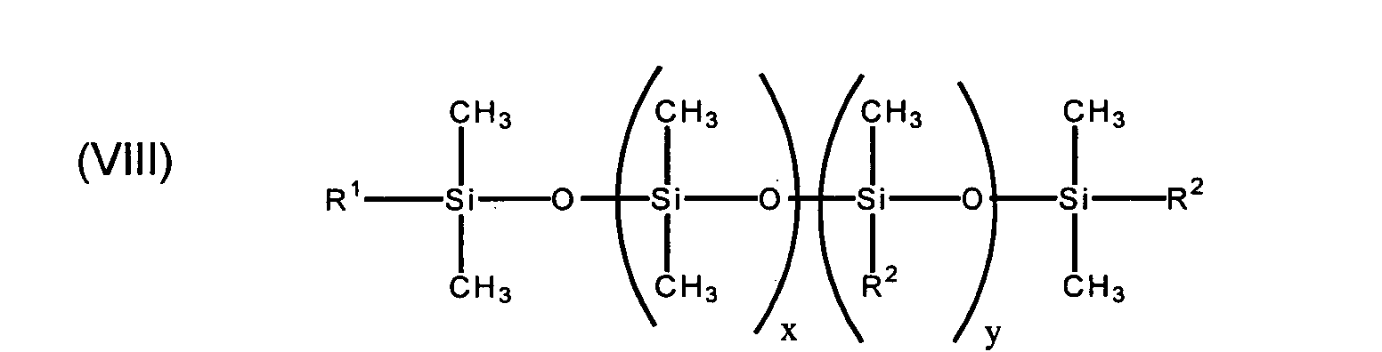 wherein R1 and R2 are independently at each occurrence selected from methylene, ethylene oxide and propylene oxide and in structure (VIII) wherein x and y are in a range between 0 and about 20 in structure (VIII).
- 56. The method of clause 45, wherein siloxane surfactant (D) comprises an ethyleneoxide functionalalized siloxane.
- 57. The method of clause 45, wherein the anhydride curing agent (C) comprises hexahydro-4-methylphthalic anhydride.
- 58. The method of clause 45, wherein the ancillary curing catalyst (E) is selected from the group consisting of an organometallic salt, a sulfonium salt, an iodonium salt, and combinations thereof.
- 59. The method of clause 45, wherein the ancillary curing catalyst (E) is selected from the group consisting of a metal carboxylate, a metal acetylacetonate, zinc octoate, stannous octoate, triarylsulfonium hexafluorophosphate, triarylsulfonium hexafluoroantimonate, diaryliodonium hexafluoroantimonate, diaryliodonium tetrakis(pentafluorophenyl)borate, and combinations thereof.
- 60. The method of clause 45, wherein the ancillary curing catalyst is zinc octoate.
- 61. The method of clause 45, further comprising at least one of thermal stabilizers, UV stabilizers, cure modifiers, coupling agents, refractive index modifiers, or combinations thereof.
- 62. The method of clause 45, comprising at least one of a thermal stabilizer, a UV stabilizer, or combination thereof.
- 63. The method of clause 45, wherein the encapsulant (11) is clear, transparent, crackfree and polishable.
- 64. The method of clause 45, wherein the encapsulant (11) has a glass transition temperature varying in a range between about 24°C and about 150°C.
- 65. The method of clause 45, wherein the encapsulant (11) has a refractive index in a range between about 0.1 and about 10.0.
- 66. A method of encapsulating a LED (1) device comprising: placing a LED (1) device into a package and providing an encapsulant (11) comprising: (A) a silicone resin comprising hydroxyfunctionalized silicone, (B) an epoxy resin comprising bisphenol F, (C) an anhydride curing agent comprising hexahydro-4-methylphthalic anhydride, (D) a siloxane surfactant comprising ethylene oxide functionalized siloxane, and (E) an ancillary curing catalyst comprising zinc octoate, wherein component (A) is present at a level of greater than about 40% by weight; component (B) is present at a level in a range of between about 1% by weight and about 20% by weight; component (C) is present at a level of less than about 40% by weight; and component (D) and (E) are present at a level in a range between about 0.008% by weight and about 10% by weight based on the combined weight of silicone resin (A), epoxy resin (B), siloxane surfactant (C), curing agent (D), and ancillary curing catalyst (E).
- 67. The method of clause 66, wherein the encapsulant (11) further comprises at least one of a thermal stabilizer, a UV stabilizer, or combination thereof.
- 68. The method of clause 66, wherein the encapsulant (11) is partially cured.
- 69. The method of clause 66, wherein the encapsulant (11) is cured.
-
Claims (10)
- A curable epoxy resin composition for encapsulation of a solid state device, which comprises (A) at least one silicone resin, (B) at least one epoxy resin, (C) at least one anhydride curing agent, (D) at least one siloxane surfactant, and (E) at least one ancillary curing catalyst.
- The composition of claim 1, wherein the silicone resin comprises a silicone resin of structure (I)wherein R is independently at each occurrence a hydroxyl group, C1-22 alkyl, C1-22 alkoxy, C2-22 alkenyl, C6-14 aryl, C6-22 alkyl-substituted aryl, C6-22 aralkyl, or OSiR3 wherein R3 is independently at each occurrence hydroxyl, C1-22 alkyl, C1-22 alkoxy, C2-22 alkenyl, C6-14 aryl, C6-22 alkyl-substituted aryl, or C6-22 aralkyl; and wherein z is in a range between about 1 and about 10.

- A curable epoxy resin composition for encapsulation of a solid state device, which comprises (A) a silicone resin comprising a hydroxyfunctional silicone resin, (B) an epoxy resin comprising bisphenol A epoxy resin, (C) an anhydride curing agent comprising hexahydro-4-methylphthalic anhydride, (D) a siloxane surfactant comprising ethylene oxide functionalized siloxane, and (E) an ancillary curing catalyst zinc octoate, wherein component (A) is present at a level of greater than about 40% by weight; component (B) is present at a level in a range of between about 1% by weight and about 20% by weight; component (C) is present at a level of less than about 40% by weight; and component (D) and (E) are present at a level in a range between about 0.008% by weight and about 10% by weight based on the combined weight of silicone resin (A), epoxy resin (B), anhydride curing agent (C), siloxane surfactant (D) and ancillary curing catalyst (E).
- The composition of claim 3 further comprising at least one of a thermal stabilizer, a UV stabilizer, or combinations thereof.
- A packaged solid state device comprising: (a) a package; (b) a chip (4); and (c) an encapsulant (11) comprising: (A) at least one silicone resin, (B) at least one epoxy resin, (C) at least one anhydride curing agent, (D) at least one siloxane surfactant, and (E) at least one ancillary curing catalyst.
- The packaged solid state device of claim 5, wherein the solid state device is a semiconductor device.
- A LED (1) device comprising: (a) a package; (b) a LED chip (4); and (c) an encapsulant (11) comprising: (A) a silicone resin comprising a hydroxyfunctional silicone resin, (B) an epoxy resin comprising a bisphenol F resin, (C) an anhydride curing agent comprising hexahydro-4-methylphthalic anhydride, (D) a siloxane surfactant comprising propylene oxide modified siloxane, and (E) a ancillary curing catalyst comprising zinc octoate, wherein component (A) is present at a level of greater than about 40% by weight; component (B) is present at a level in a range of between about 1% by weight and about 20% by weight; component (C) is present at a level of less than about 40% by weight; and component (D) and (E) are present at a level in a range between about 0.008% by weight and about 10% by weight based on the combined weight of silicone resin (A), epoxy resin (B), a siloxane surfactant (D) anhydride curing agent (C), and ancillary curing catalyst (E).
- The LED (1) of claim 7, in which the encapsulant (11) further comprises at least one of a thermal stabilizer, a UV stabilizer, or combination thereof.
- A method of encapsulating a solid state device comprising: placing a solid state device into a package; and providing an encapsulant (11) comprising: (A) at least one silicone resin, (B) at least one epoxy resin (C) at least one anhydride curing agent (D) at least one siloxane surfactant, and (E) at least one ancillary curing catalyst.
- A method of encapsulating a LED (1) device comprising: placing a LED (1) device into a package and providing an encapsulant (11) comprising: (A) a silicone resin comprising hydroxyfunctionalized silicone, (B) an epoxy resin comprising bisphenol F, (C) an anhydride curing agent comprising hexahydro-4-methylphthalic anhydride, (D) a siloxane surfactant comprising ethylene oxide functionalized siloxane, and (E) an ancillary curing catalyst comprising zinc octoate, wherein component (A) is present at a level of greater than about 40% by weight; component (B) is present at a level in a range of between about 1% by weight and about 20% by weight; component (C) is present at a level of less than about 40% by weight; and component (D) and (E) are present at a level in a range between about 0.008% by weight and about 10% by weight based on the combined weight of silicone resin (A), epoxy resin (B), siloxane surfactant (C), curing agent (D), and ancillary curing catalyst (E).
Applications Claiming Priority (2)
| Application Number | Priority Date | Filing Date | Title |
|---|---|---|---|
| US265422 | 1988-10-31 | ||
| US10/265,422 US6800373B2 (en) | 2002-10-07 | 2002-10-07 | Epoxy resin compositions, solid state devices encapsulated therewith and method |
Publications (2)
| Publication Number | Publication Date |
|---|---|
| EP1408087A1 true EP1408087A1 (en) | 2004-04-14 |
| EP1408087B1 EP1408087B1 (en) | 2007-10-10 |
Family
ID=32030326
Family Applications (1)
| Application Number | Title | Priority Date | Filing Date |
|---|---|---|---|
| EP20030256305 Expired - Lifetime EP1408087B1 (en) | 2002-10-07 | 2003-10-07 | Epoxy-polysiloxane resin compositions, solid state devices encapsulated therewith and method |
Country Status (8)
| Country | Link |
|---|---|
| US (1) | US6800373B2 (en) |
| EP (1) | EP1408087B1 (en) |
| JP (2) | JP4988141B2 (en) |
| CN (2) | CN101307183B (en) |
| AT (1) | ATE375380T1 (en) |
| DE (1) | DE60316759T2 (en) |
| ES (1) | ES2292912T3 (en) |
| TW (1) | TWI304415B (en) |
Cited By (4)
| Publication number | Priority date | Publication date | Assignee | Title |
|---|---|---|---|---|
| WO2006089540A3 (en) * | 2005-02-28 | 2006-11-02 | Osram Opto Semiconductors Gmbh | Method for producing an optical, radiation-emitting component and optical, radiation-emitting component |
| WO2007076737A1 (en) * | 2005-12-09 | 2007-07-12 | Osram Opto Semiconductors Gmbh | Optical element, production method therefor, and composite component provided with an optical element |
| US9418774B2 (en) | 2011-07-29 | 2016-08-16 | Abb Research Ltd | Curable epoxy resin composition |
| EP3486957A4 (en) * | 2016-07-14 | 2020-02-12 | Zeon Corporation | INFRARED LED |
Families Citing this family (91)
| Publication number | Priority date | Publication date | Assignee | Title |
|---|---|---|---|---|
| DE10131698A1 (en) * | 2001-06-29 | 2003-01-30 | Osram Opto Semiconductors Gmbh | Surface-mountable radiation-emitting component and method for its production |
| JP4102112B2 (en) * | 2002-06-06 | 2008-06-18 | 株式会社東芝 | Semiconductor device and manufacturing method thereof |
| US6800373B2 (en) * | 2002-10-07 | 2004-10-05 | General Electric Company | Epoxy resin compositions, solid state devices encapsulated therewith and method |
| JP3976063B2 (en) * | 2003-10-31 | 2007-09-12 | 豊田合成株式会社 | Light emitting device |
| US6946728B2 (en) * | 2004-02-19 | 2005-09-20 | Hewlett-Packard Development Company, L.P. | System and methods for hermetic sealing of post media-filled MEMS package |
| TWI257718B (en) | 2004-03-18 | 2006-07-01 | Phoseon Technology Inc | Direct cooling of LEDs |
| DE602005015884D1 (en) * | 2004-10-25 | 2009-09-17 | Dow Corning | CARBINOL FUNCTIONAL SILICONE RESINS OR ANHYDRIDE-FUNCTIONAL SILICONE RESINS CONTAINING MOLDING |
| US7807012B2 (en) * | 2004-10-25 | 2010-10-05 | Dow Corning Corporation | Moldable compositions containing carbinol functional silicone resins or anhydride functional silicone resins |
| EP1809704B1 (en) * | 2004-10-25 | 2011-08-17 | Dow Corning Corporation | Coating compositions containing a carbinol functional silicone resin or an anhydride functional silicone resin |
| JP2006156668A (en) * | 2004-11-29 | 2006-06-15 | Nichia Chem Ind Ltd | Light emitting device and manufacturing method thereof |
| JP4799883B2 (en) * | 2005-03-01 | 2011-10-26 | 日東電工株式会社 | Epoxy resin composition cured body, method for producing the same, and optical semiconductor device using the same |
| KR100830775B1 (en) * | 2005-03-01 | 2008-05-20 | 닛토덴코 가부시키가이샤 | Epoxy resin composition for photosemiconductor element encapsulation and photosemiconductor device using the same |
| JP5328159B2 (en) | 2005-03-01 | 2013-10-30 | セルカコア・ラボラトリーズ・インコーポレーテッド | Multi-wavelength sensor light emitter |
| US7429800B2 (en) * | 2005-06-30 | 2008-09-30 | Sabic Innovative Plastics Ip B.V. | Molding composition and method, and molded article |
| US7378455B2 (en) * | 2005-06-30 | 2008-05-27 | General Electric Company | Molding composition and method, and molded article |
| US20070004871A1 (en) * | 2005-06-30 | 2007-01-04 | Qiwei Lu | Curable composition and method |
| US20070045800A1 (en) * | 2005-08-19 | 2007-03-01 | Brian King | Opto-coupler with high reverse breakdown voltage and high isolation potential |
| US20070066698A1 (en) * | 2005-09-20 | 2007-03-22 | Yang Wenliang P | Dual cure compositions, methods of curing thereof and articles therefrom |
| US20070066710A1 (en) * | 2005-09-21 | 2007-03-22 | Peters Edward N | Method for electrical insulation and insulated electrical conductor |
| JP4775374B2 (en) * | 2005-11-25 | 2011-09-21 | 日立化成工業株式会社 | Liquid resin composition for electronic components and electronic component device |
| DE102005060860A1 (en) * | 2005-12-20 | 2007-06-28 | Robert Bosch Gmbh | Electronic component with potting compound |
| US8044412B2 (en) | 2006-01-20 | 2011-10-25 | Taiwan Semiconductor Manufacturing Company, Ltd | Package for a light emitting element |
| US8059006B2 (en) | 2007-05-18 | 2011-11-15 | Schweitzer Engineering Laboratories, Inc. | System and method for communicating power system information through a radio frequency device |
| US7868776B2 (en) | 2006-05-19 | 2011-01-11 | Schweitzer Engineering Laboratories, Inc. | Apparatus and system for adjusting settings of a power system device using a magnetically coupled actuator |
| MX2008014568A (en) * | 2006-05-19 | 2008-11-28 | Schweitzer Engineering Lab Inc | Faulted circuit indicator monitoring device with wireless memory monitor. |
| CA2654401C (en) | 2006-05-19 | 2013-01-08 | Schweitzer Engineering Laboratories, Inc. | Magnetic probe apparatus and method for providing a wireless connection to a detection device |
| WO2007137188A2 (en) * | 2006-05-19 | 2007-11-29 | Schweitzer Engineering Laboratories, Inc. | An article and method for providing a seal for an encapsulated device |
| US20070269219A1 (en) * | 2006-05-19 | 2007-11-22 | Teller Witold R | System and apparatus for optical communications through a semi-opaque material |
| US7692538B2 (en) * | 2006-05-19 | 2010-04-06 | Schweitzer Engineering Laboratories, Inc. | User interface for monitoring a plurality of faulted circuit indicators |
| US8033692B2 (en) * | 2006-05-23 | 2011-10-11 | Cree, Inc. | Lighting device |
| CN101089048B (en) * | 2006-06-16 | 2011-09-07 | 信越化学工业株式会社 | Epoxy-organic silicon mixed resin combination and luminous semiconductor device |
| CN100462384C (en) * | 2006-06-22 | 2009-02-18 | 上海交通大学 | A kind of preparation method of epoxy vacuum pressure impregnation resin |
| US8265723B1 (en) | 2006-10-12 | 2012-09-11 | Cercacor Laboratories, Inc. | Oximeter probe off indicator defining probe off space |
| KR100834351B1 (en) * | 2006-11-24 | 2008-06-02 | 제일모직주식회사 | Multichip package Epoxy resin composition for sealing and multichip package using the same |
| JP5143020B2 (en) * | 2006-12-04 | 2013-02-13 | パナソニック株式会社 | Sealing material and mounting structure |
| US8781544B2 (en) | 2007-03-27 | 2014-07-15 | Cercacor Laboratories, Inc. | Multiple wavelength optical sensor |
| US8374665B2 (en) | 2007-04-21 | 2013-02-12 | Cercacor Laboratories, Inc. | Tissue profile wellness monitor |
| US8337163B2 (en) * | 2007-12-05 | 2012-12-25 | General Electric Company | Fiber composite half-product with integrated elements, manufacturing method therefor and use thereof |
| US8665102B2 (en) | 2008-07-18 | 2014-03-04 | Schweitzer Engineering Laboratories Inc | Transceiver interface for power system monitoring |
| JP5410732B2 (en) * | 2008-09-30 | 2014-02-05 | 東京応化工業株式会社 | Photosensitive resin composition and sealant |
| US8079820B2 (en) * | 2008-12-18 | 2011-12-20 | General Electric Company | Blade module, a modular rotor blade and a method for assembling a modular rotor blade |
| JP2010163566A (en) * | 2009-01-16 | 2010-07-29 | Three M Innovative Properties Co | Epoxy resin composition |
| KR101616898B1 (en) * | 2009-03-05 | 2016-04-29 | 신닛테츠 수미킨 가가쿠 가부시키가이샤 | Epoxy resin composition |
| JP5556133B2 (en) * | 2009-03-31 | 2014-07-23 | 日立化成株式会社 | Liquid resin composition for electronic components and electronic component device |
| KR101151063B1 (en) * | 2009-03-31 | 2012-06-01 | 히다치 가세고교 가부시끼가이샤 | Liquid resin composition for electronic component and electronic component device |
| US9839381B1 (en) | 2009-11-24 | 2017-12-12 | Cercacor Laboratories, Inc. | Physiological measurement system with automatic wavelength adjustment |
| GB2487882B (en) | 2009-12-04 | 2017-03-29 | Masimo Corp | Calibration for multi-stage physiological monitors |
| TWI408174B (en) * | 2010-02-09 | 2013-09-11 | Nanya Plastics Corp | Epoxy-silicone resin composition for optical encapsulation and coating |
| JP5700689B2 (en) * | 2010-02-10 | 2015-04-15 | リンテック株式会社 | Curable composition, cured product and method of using curable composition |
| WO2011111293A1 (en) * | 2010-03-10 | 2011-09-15 | パナソニック株式会社 | Led-packaging resin body, led device, and method for manufacturing led device |
| WO2011118109A1 (en) * | 2010-03-23 | 2011-09-29 | 株式会社朝日ラバー | Flexible reflective substrate, manufacturing method for same, and base material composition for use in reflective substrate |
| WO2011163100A2 (en) * | 2010-06-23 | 2011-12-29 | Dow Global Technologies Llc | Powder coatings compositions |
| CN103080181B (en) | 2010-06-28 | 2017-04-12 | 蓝立方知识产权有限责任公司 | curable resin composition |
| CN102339936B (en) * | 2010-07-27 | 2015-04-29 | 展晶科技(深圳)有限公司 | Package structure for light-emitting device and method for manufacturing same |
| US20120040106A1 (en) | 2010-08-16 | 2012-02-16 | Stefan Simmerer | Apparatus for impregnating a fiber material with a resin and methods for forming a fiber-reinforced plastic part |
| DE102010046281A1 (en) | 2010-09-21 | 2012-03-22 | Ntc Nano Tech Coatings Gmbh | Pigmented two-component protective coating |
| JP2013539229A (en) * | 2010-09-29 | 2013-10-17 | コーニンクレッカ フィリップス エヌ ヴェ | Wavelength conversion light emitting device |
| CN102443246B (en) * | 2010-10-13 | 2014-01-22 | 明德国际仓储贸易(上海)有限公司 | Silicon-containing resin packaging composition |
| DE102010042588A1 (en) | 2010-10-18 | 2012-04-19 | Everlight Usa, Inc. | Silicone containing encapsulating composition useful for light emitting diode encapsulation, comprises epoxy resin, acid anhydride curing agent, carbinol-siloxane resin, and reactive UV absorbent or hindered amine reactive light stabilizer |
| CN102030970A (en) * | 2010-11-23 | 2011-04-27 | 上海旌纬微电子科技有限公司 | Epoxy resin composition for packaging electronic element and preparation method thereof |
| JP5832740B2 (en) * | 2010-11-30 | 2015-12-16 | 株式会社ダイセル | Curable epoxy resin composition |
| EP2760910A4 (en) * | 2011-09-28 | 2015-12-16 | Henkel Ag & Co Kgaa | OXETANE CONTAINING COMPOUNDS AND COMPOSITIONS BASED THEREON |
| US20120138223A1 (en) | 2011-09-29 | 2012-06-07 | General Electric Company | Uv-ir combination curing system and method of use for wind blade manufacture and repair |
| CN102516501A (en) * | 2011-11-22 | 2012-06-27 | 中国科学院上海有机化学研究所 | Photo-curing material for manufacturing light-emitting diode (LED) lens |
| US8526156B2 (en) | 2011-12-21 | 2013-09-03 | Schweitzer Engineering Laboratories Inc | High speed signaling of power system conditions |
| JP6047294B2 (en) * | 2012-03-30 | 2016-12-21 | 株式会社ダイセル | Curable epoxy resin composition |
| JP5899025B2 (en) * | 2012-03-30 | 2016-04-06 | 株式会社ダイセル | Curable epoxy resin composition |
| DE102012211323A1 (en) * | 2012-06-29 | 2014-01-02 | Evonik Industries Ag | Hardener for epoxy resin systems and their use |
| DE102012214440B3 (en) | 2012-08-14 | 2013-10-24 | Fraunhofer-Gesellschaft zur Förderung der angewandten Forschung e.V. | Planar optical element, sensor element and method for its production |
| CN102775736A (en) * | 2012-08-16 | 2012-11-14 | 上纬(上海)精细化工有限公司 | LED (Light-Emitting Diode) package material and composite used in same |
| CN103665882B (en) * | 2012-09-19 | 2016-04-20 | 浙江三元电子科技有限公司 | A kind of thermally conductive silicone rubber composite material, heat-conducting silica gel sheet and preparation method thereof |
| CN102916117B (en) * | 2012-09-25 | 2015-08-26 | 中山大学 | Improve Color-spatial distribution and light extraction efficiency multimodal spectrum LED and manufacture method |
| JP6279830B2 (en) * | 2012-11-12 | 2018-02-14 | 日本化薬株式会社 | Curable resin composition and cured product thereof |
| WO2014104719A1 (en) | 2012-12-26 | 2014-07-03 | 제일모직 주식회사 | Curable polysiloxane composition for optical instrument, packaging material, and optical instrument |
| FR3000408B1 (en) * | 2013-01-03 | 2015-02-27 | Commissariat Energie Atomique | METHOD FOR PRODUCING FILTER FOR FILTRATION OF NANOPARTICLES, FILTER OBTAINED AND METHOD FOR COLLECTING AND QUANTITATIVE ANALYSIS OF NANOPARTICLES THEREOF |
| JP6046497B2 (en) * | 2013-01-09 | 2016-12-14 | 株式会社ダイセル | Curable epoxy resin composition |
| US20140254135A1 (en) * | 2013-03-08 | 2014-09-11 | Shat-R-Shield, Inc. | Light-emitting diode light and heat device |
| US9698314B2 (en) * | 2013-03-15 | 2017-07-04 | General Electric Company | Color stable red-emitting phosphors |
| JP6478449B2 (en) | 2013-08-21 | 2019-03-06 | キヤノン株式会社 | Device manufacturing method and device manufacturing method |
| DE102013222003A1 (en) * | 2013-10-29 | 2015-04-30 | Evonik Industries Ag | Means for the sealing of light-emitting diodes |
| CN104292755B (en) * | 2014-10-16 | 2017-02-01 | 苏州思莱特电子科技有限公司 | High-molecule LED (Light-Emitting Diode) packaging material and preparation method thereof |
| CN106008979A (en) * | 2015-03-27 | 2016-10-12 | 豪雅冠得股份有限公司 | Curable resin composition and optical semiconductor device |
| US9871173B2 (en) | 2015-06-18 | 2018-01-16 | Cree, Inc. | Light emitting devices having closely-spaced broad-spectrum and narrow-spectrum luminescent materials and related methods |
| KR101778848B1 (en) * | 2015-08-21 | 2017-09-14 | 엘지전자 주식회사 | Light emitting device package assembly and method of fabricating the same |
| KR101933273B1 (en) * | 2016-05-30 | 2018-12-27 | 삼성에스디아이 주식회사 | Epoxy resin composition for encapsulating semiconductor device and semiconductor device encapsulated by using the same |
| JP2018030999A (en) * | 2017-08-04 | 2018-03-01 | 日本化薬株式会社 | Curable resin composition and cured product thereof |
| US10541353B2 (en) | 2017-11-10 | 2020-01-21 | Cree, Inc. | Light emitting devices including narrowband converters for outdoor lighting applications |
| KR102146997B1 (en) * | 2017-12-29 | 2020-08-21 | 삼성에스디아이 주식회사 | Epoxy resin composition for encapsulating semiconductor device and semiconductor device encapsulated using the same |
| CN110149434B (en) * | 2018-02-13 | 2021-09-14 | 深圳富泰宏精密工业有限公司 | Electronic device and preparation method thereof |
| US11397198B2 (en) | 2019-08-23 | 2022-07-26 | Schweitzer Engineering Laboratories, Inc. | Wireless current sensor |
| WO2021261427A1 (en) * | 2020-06-22 | 2021-12-30 | 日東電工株式会社 | Optical element joining-reinforcing resin composition and optical module using same |
Citations (5)
| Publication number | Priority date | Publication date | Assignee | Title |
|---|---|---|---|---|
| GB2072190A (en) * | 1980-03-21 | 1981-09-30 | Toray Silicone Co | Siloxane-modified Epoxy Resin Composition |
| EP0385736A2 (en) * | 1989-03-02 | 1990-09-05 | Rohm And Haas Company | Epoxy encapsulant compositions and low stress additives therefor |
| US6048946A (en) * | 1997-08-27 | 2000-04-11 | Ciba Specialty Chemicals Corp. | Hydrophobic epoxy resin system |
| US20020022681A1 (en) * | 2000-07-05 | 2002-02-21 | Nobuhiro Ichiroku | Epoxy resin composition |
| US20030071366A1 (en) * | 2001-08-21 | 2003-04-17 | General Electric Company | Epoxy resin compositions, solid state devices encapsulated therewith and method |
Family Cites Families (20)
| Publication number | Priority date | Publication date | Assignee | Title |
|---|---|---|---|---|
| JPH0682764B2 (en) * | 1985-11-28 | 1994-10-19 | 日東電工株式会社 | Semiconductor device |
| DE3634084A1 (en) * | 1986-10-07 | 1988-04-21 | Hanse Chemie Gmbh | MODIFIED REACTION RESIN, METHOD FOR PRODUCING IT AND ITS USE |
| JPH0725866B2 (en) * | 1988-04-19 | 1995-03-22 | サンスター技研株式会社 | Epoxy resin composition |
| JP2760889B2 (en) * | 1989-12-28 | 1998-06-04 | 日東電工株式会社 | Optical semiconductor device |
| EP0624183A1 (en) * | 1992-01-29 | 1994-11-17 | The Dow Chemical Company | Modified epoxy resin compositions, reduced gloss coating compositions |
| JPH065464A (en) * | 1992-06-19 | 1994-01-14 | Hitachi Chem Co Ltd | Epoxy resin composition for capacitor |
| JPH06296044A (en) * | 1993-04-08 | 1994-10-21 | Matsushita Electric Ind Co Ltd | Epoxy resin composition for led |
| JP3399095B2 (en) * | 1994-07-04 | 2003-04-21 | 新日本理化株式会社 | Liquid epoxy resin composition |
| DE19523897C2 (en) * | 1995-06-30 | 2002-10-24 | Bosch Gmbh Robert | Use of silicone-modified epoxy resins as casting compounds for electrotechnical or electronic components |
| JPH09118738A (en) * | 1995-10-25 | 1997-05-06 | Nippon Kayaku Co Ltd | Low-stress resin composition |
| JP2710921B2 (en) * | 1995-11-13 | 1998-02-10 | 日東電工株式会社 | Semiconductor device |
| JP3592825B2 (en) * | 1996-02-07 | 2004-11-24 | 東レ・ダウコーニング・シリコーン株式会社 | Curable epoxy resin composition and electronic component |
| JP3957760B2 (en) * | 1996-07-10 | 2007-08-15 | 統寶光電股▲ふん▼有限公司 | Siloxanes and siloxane derivatives as encapsulants for organic light emitting devices |
| DE69934153T2 (en) * | 1998-02-02 | 2007-09-20 | Shin-Etsu Chemical Co., Ltd. | Method for mounting flip-chip semiconductor devices |
| US6204523B1 (en) * | 1998-11-06 | 2001-03-20 | Lumileds Lighting, U.S., Llc | High stability optical encapsulation and packaging for light-emitting diodes in the green, blue, and near UV range |
| JP2000204137A (en) * | 1999-01-14 | 2000-07-25 | Toto Ltd | Resin molded product, resin molded article and their production |
| JP3397176B2 (en) * | 1999-06-25 | 2003-04-14 | 松下電工株式会社 | Liquid epoxy resin composition and semiconductor device |
| RU2275401C2 (en) * | 2001-03-13 | 2006-04-27 | Джей Эс Эр КОРПОРЕЙШН | Radiation sensitive compositions varying refractory index and use thereof |
| US6624216B2 (en) * | 2002-01-31 | 2003-09-23 | National Starch And Chemical Investment Holding Corporation | No-flow underfill encapsulant |
| US6800373B2 (en) * | 2002-10-07 | 2004-10-05 | General Electric Company | Epoxy resin compositions, solid state devices encapsulated therewith and method |
-
2002
- 2002-10-07 US US10/265,422 patent/US6800373B2/en not_active Expired - Fee Related
-
2003
- 2003-10-06 JP JP2003346640A patent/JP4988141B2/en not_active Expired - Fee Related
- 2003-10-07 ES ES03256305T patent/ES2292912T3/en not_active Expired - Lifetime
- 2003-10-07 DE DE2003616759 patent/DE60316759T2/en not_active Expired - Lifetime
- 2003-10-07 EP EP20030256305 patent/EP1408087B1/en not_active Expired - Lifetime
- 2003-10-07 AT AT03256305T patent/ATE375380T1/en active
- 2003-10-07 TW TW92127812A patent/TWI304415B/en not_active IP Right Cessation
- 2003-10-08 CN CN2008100993536A patent/CN101307183B/en not_active Expired - Fee Related
- 2003-10-08 CN CNB200310113881XA patent/CN100480352C/en not_active Expired - Fee Related
-
2010
- 2010-05-24 JP JP2010118625A patent/JP2010202880A/en active Pending
Patent Citations (5)
| Publication number | Priority date | Publication date | Assignee | Title |
|---|---|---|---|---|
| GB2072190A (en) * | 1980-03-21 | 1981-09-30 | Toray Silicone Co | Siloxane-modified Epoxy Resin Composition |
| EP0385736A2 (en) * | 1989-03-02 | 1990-09-05 | Rohm And Haas Company | Epoxy encapsulant compositions and low stress additives therefor |
| US6048946A (en) * | 1997-08-27 | 2000-04-11 | Ciba Specialty Chemicals Corp. | Hydrophobic epoxy resin system |
| US20020022681A1 (en) * | 2000-07-05 | 2002-02-21 | Nobuhiro Ichiroku | Epoxy resin composition |
| US20030071366A1 (en) * | 2001-08-21 | 2003-04-17 | General Electric Company | Epoxy resin compositions, solid state devices encapsulated therewith and method |
Cited By (6)
| Publication number | Priority date | Publication date | Assignee | Title |
|---|---|---|---|---|
| WO2006089540A3 (en) * | 2005-02-28 | 2006-11-02 | Osram Opto Semiconductors Gmbh | Method for producing an optical, radiation-emitting component and optical, radiation-emitting component |
| US8247263B2 (en) | 2005-02-28 | 2012-08-21 | Osram Opto Semiconductors Gmbh | Method for producing an optical, radiation-emitting component and optical, radiation-emitting component |
| WO2007076737A1 (en) * | 2005-12-09 | 2007-07-12 | Osram Opto Semiconductors Gmbh | Optical element, production method therefor, and composite component provided with an optical element |
| US7974018B2 (en) | 2005-12-09 | 2011-07-05 | Osram Opto Semiconductors Gmbh | Optical element, production method therefor, and composite component provided with an optical element |
| US9418774B2 (en) | 2011-07-29 | 2016-08-16 | Abb Research Ltd | Curable epoxy resin composition |
| EP3486957A4 (en) * | 2016-07-14 | 2020-02-12 | Zeon Corporation | INFRARED LED |
Also Published As
| Publication number | Publication date |
|---|---|
| CN100480352C (en) | 2009-04-22 |
| TWI304415B (en) | 2008-12-21 |
| DE60316759D1 (en) | 2007-11-22 |
| JP2010202880A (en) | 2010-09-16 |
| ATE375380T1 (en) | 2007-10-15 |
| CN101307183B (en) | 2011-06-29 |
| DE60316759T2 (en) | 2008-07-17 |
| US6800373B2 (en) | 2004-10-05 |
| CN101307183A (en) | 2008-11-19 |
| EP1408087B1 (en) | 2007-10-10 |
| US20040067366A1 (en) | 2004-04-08 |
| ES2292912T3 (en) | 2008-03-16 |
| TW200415019A (en) | 2004-08-16 |
| JP4988141B2 (en) | 2012-08-01 |
| JP2004277697A (en) | 2004-10-07 |
| CN1534074A (en) | 2004-10-06 |
Similar Documents
| Publication | Publication Date | Title |
|---|---|---|
| US6800373B2 (en) | Epoxy resin compositions, solid state devices encapsulated therewith and method | |
| US6632892B2 (en) | Composition comprising silicone epoxy resin, hydroxyl compound, anhydride and curing catalyst | |
| US6617400B2 (en) | Composition of cycloaliphatic epoxy resin, anhydride curing agent and boron catalyst | |
| EP1285938B1 (en) | Epoxy resin encapsulation compositions | |
| US6507049B1 (en) | Encapsulants for solid state devices | |
| JP2008007782A (en) | Optoelectronic devices | |
| WO2003091338A1 (en) | Hardenable composition, hardening product, process for producing the same and light emitting diode sealed with the hardening product | |
| KR20160094368A (en) | Heat-curable resin composition for optical semiconductor device, lead frame for optical semiconductor device and obtained using same, and optical semiconductor device | |
| US20070299162A1 (en) | Optoelectronic device | |
| US20080160317A1 (en) | Optoelectronic device | |
| US20070295956A1 (en) | Optoelectronic device | |
| KR20160019407A (en) | Epoxy resin composition for optical semiconductor reflectors, thermosetting resin composition for optical semiconductor devices, lead frame for optical semiconductor devices obtained using said thermosetting resin composition for optical semiconductor devices, sealed optical semiconductor element, and optical semiconductor device | |
| US20070295983A1 (en) | Optoelectronic device | |
| US20080001140A1 (en) | Optoelectronic device | |
| KR20170023334A (en) | Organopolysiloxane composition | |
| KR102703006B1 (en) | Addition-curable siloxane composition |
Legal Events
| Date | Code | Title | Description |
|---|---|---|---|
| PUAI | Public reference made under article 153(3) epc to a published international application that has entered the european phase |
Free format text: ORIGINAL CODE: 0009012 |
|
| AK | Designated contracting states |
Kind code of ref document: A1 Designated state(s): AT BE BG CH CY CZ DE DK EE ES FI FR GB GR HU IE IT LI LU MC NL PT RO SE SI SK TR |
|
| AX | Request for extension of the european patent |
Extension state: AL LT LV MK |
|
| 17P | Request for examination filed |
Effective date: 20041014 |
|
| 17Q | First examination report despatched |
Effective date: 20041117 |
|
| AKX | Designation fees paid |
Designated state(s): AT BE BG CH CY CZ DE DK EE ES FI FR GB GR HU IE IT LI LU MC NL PT RO SE SI SK TR |
|
| GRAP | Despatch of communication of intention to grant a patent |
Free format text: ORIGINAL CODE: EPIDOSNIGR1 |
|
| GRAS | Grant fee paid |
Free format text: ORIGINAL CODE: EPIDOSNIGR3 |
|
| GRAA | (expected) grant |
Free format text: ORIGINAL CODE: 0009210 |
|
| AK | Designated contracting states |
Kind code of ref document: B1 Designated state(s): AT BE BG CH CY CZ DE DK EE ES FI FR GB GR HU IE IT LI LU MC NL PT RO SE SI SK TR |
|
| REG | Reference to a national code |
Ref country code: GB Ref legal event code: FG4D |
|
| REG | Reference to a national code |
Ref country code: CH Ref legal event code: EP |
|
| REG | Reference to a national code |
Ref country code: IE Ref legal event code: FG4D |
|
| REF | Corresponds to: |
Ref document number: 60316759 Country of ref document: DE Date of ref document: 20071122 Kind code of ref document: P |
|
| REG | Reference to a national code |
Ref country code: CH Ref legal event code: NV Representative=s name: BOVARD AG PATENTANWAELTE |
|
| REG | Reference to a national code |
Ref country code: SE Ref legal event code: TRGR |
|
| REG | Reference to a national code |
Ref country code: ES Ref legal event code: FG2A Ref document number: 2292912 Country of ref document: ES Kind code of ref document: T3 |
|
| PG25 | Lapsed in a contracting state [announced via postgrant information from national office to epo] |
Ref country code: PT Free format text: LAPSE BECAUSE OF FAILURE TO SUBMIT A TRANSLATION OF THE DESCRIPTION OR TO PAY THE FEE WITHIN THE PRESCRIBED TIME-LIMIT Effective date: 20080310 Ref country code: BG Free format text: LAPSE BECAUSE OF FAILURE TO SUBMIT A TRANSLATION OF THE DESCRIPTION OR TO PAY THE FEE WITHIN THE PRESCRIBED TIME-LIMIT Effective date: 20080110 |
|
| ET | Fr: translation filed | ||
| PG25 | Lapsed in a contracting state [announced via postgrant information from national office to epo] |
Ref country code: DK Free format text: LAPSE BECAUSE OF FAILURE TO SUBMIT A TRANSLATION OF THE DESCRIPTION OR TO PAY THE FEE WITHIN THE PRESCRIBED TIME-LIMIT Effective date: 20071010 Ref country code: CZ Free format text: LAPSE BECAUSE OF FAILURE TO SUBMIT A TRANSLATION OF THE DESCRIPTION OR TO PAY THE FEE WITHIN THE PRESCRIBED TIME-LIMIT Effective date: 20071010 |
|
| PLBE | No opposition filed within time limit |
Free format text: ORIGINAL CODE: 0009261 |
|
| STAA | Information on the status of an ep patent application or granted ep patent |
Free format text: STATUS: NO OPPOSITION FILED WITHIN TIME LIMIT |
|
| PG25 | Lapsed in a contracting state [announced via postgrant information from national office to epo] |
Ref country code: RO Free format text: LAPSE BECAUSE OF FAILURE TO SUBMIT A TRANSLATION OF THE DESCRIPTION OR TO PAY THE FEE WITHIN THE PRESCRIBED TIME-LIMIT Effective date: 20071010 Ref country code: SK Free format text: LAPSE BECAUSE OF FAILURE TO SUBMIT A TRANSLATION OF THE DESCRIPTION OR TO PAY THE FEE WITHIN THE PRESCRIBED TIME-LIMIT Effective date: 20071010 |
|
| 26N | No opposition filed |
Effective date: 20080711 |
|
| PG25 | Lapsed in a contracting state [announced via postgrant information from national office to epo] |
Ref country code: GR Free format text: LAPSE BECAUSE OF FAILURE TO SUBMIT A TRANSLATION OF THE DESCRIPTION OR TO PAY THE FEE WITHIN THE PRESCRIBED TIME-LIMIT Effective date: 20080111 |
|
| PG25 | Lapsed in a contracting state [announced via postgrant information from national office to epo] |
Ref country code: EE Free format text: LAPSE BECAUSE OF FAILURE TO SUBMIT A TRANSLATION OF THE DESCRIPTION OR TO PAY THE FEE WITHIN THE PRESCRIBED TIME-LIMIT Effective date: 20071010 |
|
| PG25 | Lapsed in a contracting state [announced via postgrant information from national office to epo] |
Ref country code: MC Free format text: LAPSE BECAUSE OF NON-PAYMENT OF DUE FEES Effective date: 20081031 |
|
| PG25 | Lapsed in a contracting state [announced via postgrant information from national office to epo] |
Ref country code: SI Free format text: LAPSE BECAUSE OF FAILURE TO SUBMIT A TRANSLATION OF THE DESCRIPTION OR TO PAY THE FEE WITHIN THE PRESCRIBED TIME-LIMIT Effective date: 20071010 |
|
| PG25 | Lapsed in a contracting state [announced via postgrant information from national office to epo] |
Ref country code: CY Free format text: LAPSE BECAUSE OF FAILURE TO SUBMIT A TRANSLATION OF THE DESCRIPTION OR TO PAY THE FEE WITHIN THE PRESCRIBED TIME-LIMIT Effective date: 20071010 |
|
| PG25 | Lapsed in a contracting state [announced via postgrant information from national office to epo] |
Ref country code: HU Free format text: LAPSE BECAUSE OF FAILURE TO SUBMIT A TRANSLATION OF THE DESCRIPTION OR TO PAY THE FEE WITHIN THE PRESCRIBED TIME-LIMIT Effective date: 20080411 Ref country code: LU Free format text: LAPSE BECAUSE OF NON-PAYMENT OF DUE FEES Effective date: 20081007 |
|
| PG25 | Lapsed in a contracting state [announced via postgrant information from national office to epo] |
Ref country code: TR Free format text: LAPSE BECAUSE OF FAILURE TO SUBMIT A TRANSLATION OF THE DESCRIPTION OR TO PAY THE FEE WITHIN THE PRESCRIBED TIME-LIMIT Effective date: 20071010 |
|
| REG | Reference to a national code |
Ref country code: CH Ref legal event code: PFA Owner name: GENERAL ELECTRIC COMPANY Free format text: GENERAL ELECTRIC COMPANY#1 RIVER ROAD#SCHENECTADY, NY 12345 (US) -TRANSFER TO- GENERAL ELECTRIC COMPANY#1 RIVER ROAD#SCHENECTADY, NY 12345 (US) |
|
| REG | Reference to a national code |
Ref country code: FR Ref legal event code: PLFP Year of fee payment: 13 |
|
| REG | Reference to a national code |
Ref country code: FR Ref legal event code: PLFP Year of fee payment: 14 |
|
| REG | Reference to a national code |
Ref country code: FR Ref legal event code: PLFP Year of fee payment: 15 |
|
| REG | Reference to a national code |
Ref country code: FR Ref legal event code: PLFP Year of fee payment: 16 |
|
| PGFP | Annual fee paid to national office [announced via postgrant information from national office to epo] |
Ref country code: NL Payment date: 20201026 Year of fee payment: 18 |
|
| PGFP | Annual fee paid to national office [announced via postgrant information from national office to epo] |
Ref country code: IT Payment date: 20201023 Year of fee payment: 18 Ref country code: FR Payment date: 20201026 Year of fee payment: 18 Ref country code: GB Payment date: 20201027 Year of fee payment: 18 Ref country code: AT Payment date: 20200921 Year of fee payment: 18 Ref country code: IE Payment date: 20201027 Year of fee payment: 18 Ref country code: CH Payment date: 20201103 Year of fee payment: 18 Ref country code: FI Payment date: 20201028 Year of fee payment: 18 Ref country code: DE Payment date: 20201028 Year of fee payment: 18 Ref country code: SE Payment date: 20201028 Year of fee payment: 18 Ref country code: ES Payment date: 20201103 Year of fee payment: 18 |
|
| PGFP | Annual fee paid to national office [announced via postgrant information from national office to epo] |
Ref country code: BE Payment date: 20201027 Year of fee payment: 18 |
|
| REG | Reference to a national code |
Ref country code: DE Ref legal event code: R119 Ref document number: 60316759 Country of ref document: DE |
|
| REG | Reference to a national code |
Ref country code: FI Ref legal event code: MAE |
|
| REG | Reference to a national code |
Ref country code: SE Ref legal event code: EUG |
|
| REG | Reference to a national code |
Ref country code: NL Ref legal event code: MM Effective date: 20211101 |
|
| REG | Reference to a national code |
Ref country code: CH Ref legal event code: PL Ref country code: AT Ref legal event code: MM01 Ref document number: 375380 Country of ref document: AT Kind code of ref document: T Effective date: 20211007 |
|
| REG | Reference to a national code |
Ref country code: BE Ref legal event code: MM Effective date: 20211031 |
|
| GBPC | Gb: european patent ceased through non-payment of renewal fee |
Effective date: 20211007 |
|
| PG25 | Lapsed in a contracting state [announced via postgrant information from national office to epo] |
Ref country code: SE Free format text: LAPSE BECAUSE OF NON-PAYMENT OF DUE FEES Effective date: 20211008 Ref country code: NL Free format text: LAPSE BECAUSE OF NON-PAYMENT OF DUE FEES Effective date: 20211101 Ref country code: GB Free format text: LAPSE BECAUSE OF NON-PAYMENT OF DUE FEES Effective date: 20211007 Ref country code: DE Free format text: LAPSE BECAUSE OF NON-PAYMENT OF DUE FEES Effective date: 20220503 Ref country code: BE Free format text: LAPSE BECAUSE OF NON-PAYMENT OF DUE FEES Effective date: 20211031 |
|
| PG25 | Lapsed in a contracting state [announced via postgrant information from national office to epo] |
Ref country code: LI Free format text: LAPSE BECAUSE OF NON-PAYMENT OF DUE FEES Effective date: 20211031 Ref country code: FI Free format text: LAPSE BECAUSE OF NON-PAYMENT OF DUE FEES Effective date: 20211007 Ref country code: CH Free format text: LAPSE BECAUSE OF NON-PAYMENT OF DUE FEES Effective date: 20211031 Ref country code: AT Free format text: LAPSE BECAUSE OF NON-PAYMENT OF DUE FEES Effective date: 20211007 |
|
| PG25 | Lapsed in a contracting state [announced via postgrant information from national office to epo] |
Ref country code: FR Free format text: LAPSE BECAUSE OF NON-PAYMENT OF DUE FEES Effective date: 20211031 |
|
| PG25 | Lapsed in a contracting state [announced via postgrant information from national office to epo] |
Ref country code: IE Free format text: LAPSE BECAUSE OF NON-PAYMENT OF DUE FEES Effective date: 20211007 |
|
| REG | Reference to a national code |
Ref country code: ES Ref legal event code: FD2A Effective date: 20221125 |
|
| PG25 | Lapsed in a contracting state [announced via postgrant information from national office to epo] |
Ref country code: ES Free format text: LAPSE BECAUSE OF NON-PAYMENT OF DUE FEES Effective date: 20211008 |
|
| PG25 | Lapsed in a contracting state [announced via postgrant information from national office to epo] |
Ref country code: IT Free format text: LAPSE BECAUSE OF NON-PAYMENT OF DUE FEES Effective date: 20211031 |