EP1405394B1 - Isolierte treiberschaltungsanordnung zur verwendung in leistungsschaltreglern - Google Patents
Isolierte treiberschaltungsanordnung zur verwendung in leistungsschaltreglern Download PDFInfo
- Publication number
- EP1405394B1 EP1405394B1 EP02709247A EP02709247A EP1405394B1 EP 1405394 B1 EP1405394 B1 EP 1405394B1 EP 02709247 A EP02709247 A EP 02709247A EP 02709247 A EP02709247 A EP 02709247A EP 1405394 B1 EP1405394 B1 EP 1405394B1
- Authority
- EP
- European Patent Office
- Prior art keywords
- primary
- switch
- input
- drive transformer
- winding
- Prior art date
- Legal status (The legal status is an assumption and is not a legal conclusion. Google has not performed a legal analysis and makes no representation as to the accuracy of the status listed.)
- Expired - Lifetime
Links
Images


Classifications
-
- H—ELECTRICITY
- H02—GENERATION; CONVERSION OR DISTRIBUTION OF ELECTRIC POWER
- H02M—APPARATUS FOR CONVERSION BETWEEN AC AND AC, BETWEEN AC AND DC, OR BETWEEN DC AND DC, AND FOR USE WITH MAINS OR SIMILAR POWER SUPPLY SYSTEMS; CONVERSION OF DC OR AC INPUT POWER INTO SURGE OUTPUT POWER; CONTROL OR REGULATION THEREOF
- H02M1/00—Details of apparatus for conversion
- H02M1/08—Circuits specially adapted for the generation of control voltages for semiconductor devices incorporated in static converters
- H02M1/088—Circuits specially adapted for the generation of control voltages for semiconductor devices incorporated in static converters for the simultaneous control of series or parallel connected semiconductor devices
-
- H—ELECTRICITY
- H02—GENERATION; CONVERSION OR DISTRIBUTION OF ELECTRIC POWER
- H02M—APPARATUS FOR CONVERSION BETWEEN AC AND AC, BETWEEN AC AND DC, OR BETWEEN DC AND DC, AND FOR USE WITH MAINS OR SIMILAR POWER SUPPLY SYSTEMS; CONVERSION OF DC OR AC INPUT POWER INTO SURGE OUTPUT POWER; CONTROL OR REGULATION THEREOF
- H02M1/00—Details of apparatus for conversion
- H02M1/38—Means for preventing simultaneous conduction of switches
Definitions
- This invention relates generally to switch-mode power converters and more particularly it provides simple a drive circuit and an enable function with isolation and having high performance in full-bridge topologies using synchronous rectification.
- a switch-mode power converter is a circuit that uses an inductor, a transformer, or a capacitor, or some combination, as energy storage elements to transfer energy from an input source to an output load in discrete pulses. Additional circuitry is added to maintain a constant voltage within the load limits of the circuit.
- the basic circuit can be configured to step up (boost), step down (buck), or invert output voltage with respect to input voltage. Using a transformer allows the output voltage to be electrically isolated from the input voltage.
- Switch-mode converters have changed very little over the past 15 years, most using Schottky diodes to rectify their output.
- newer challenges in the industry for dc/dc power supply designers demand lower voltages required by digital circuits, and also higher frequencies.
- Since converters using Schottky diodes for rectification experience a large forward voltage drop relative to the output voltage, their efficiency is generally relatively low. Lower efficiencies result in more dissipated heat that has to be removed using a heat sink, which takes up space.
- a dramatic increase in converter efficiency can be accomplished by replacing the Schottky diodes with "synchronous rectifiers" realized in practice with MOSFET transistors. Synchronous rectifiers are not new, but they have previously been too expensive to justify, primarily due to high "on" resistance. However, as costs fall and performance improves, synchronous rectifiers have quickly become a viable component, especially for low voltage converters.
- a third reason why self driven synchronous rectifiers have not been a preferred solution is that the drive voltage, being derived from a power transformer, depends on input voltage and therefore could vary significantly (200% to 300%). As a consequence, power consumption of the drive circuit, which varies exponentially with input voltage, can vary even more (400% to 900%) and decrease overall converter efficiency.
- a much more preferred solution is to use direct drive to power synchronous rectifiers with well-controlled timing between drive signals for the main switches (primary side) and synchronous rectifiers (secondary side). This solution thus allows for very efficient operation of the synchronous rectifiers even at high switching frequencies. Yet another benefit of direct driven synchronous rectifiers is that the drive voltage (gate to source) is constant and independent of input voltage, which further improves efficiency over a wide input voltage range.
- DE-A-4327073 describes a chopper circuit for the electrically insulated transmission of bipolar measurement currents and arranged such that a direct current at an input is chopped and transmitted via a push-pull transformer to a synchronous rectifier circuit.
- the synchronous rectifier circuit comprises rectifiers controlled by the outputs of windings of a control transformer driven by an oscillator which also controls the chopper circuit.
- HP-A-957568 describes a switching power source in which the output from a secondary winding is rectified using switching transistors controlled via the outputs from transformer windings.
- one drive transformer is used for providing appropriate delays as well as providing power for driving primary switches, particularly high side switches in a full-bridge topology.
- the leakage inductance of the drive transformer is used to delay turn-on of the main switches (primary side) while turn-off is with no significant delay.
- the number of windings on the drive transformer is minimized to four, when the control circuit is referenced to the output of the converter, and minimized to five when the control circuit is referenced to the input of the converter.
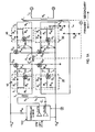
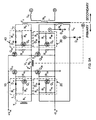
- Figs. 1 A and 1B demonstrate a full-bridge topology with synchronous rectifiers using an isolated drive circuit according to an embodiment of the invention.
- Four primary switches (transistors) Q 10 , Q 20 , Q 30 and Q 40 , power transformer T 2 , synchronous rectifiers S 1 and S 2 , output inductor L 0 , and capacitor C 0 form the power stage of the full-bridge converter.
- Switches Q 10 and Q 20 form one leg of the bridge, while switches Q 30 and Q 40 form the other leg of the bridge. Both legs of the bridge are connected across the input voltage, with Q 10 and Q 40 connected to the positive side and Q 20 and Q 30 connected to the negative side.
- Switches in the same leg always conduct out of phase, while diagonal switches conduct simultaneously (Q 10 and Q 30 , and Q 20 and Q 40 ).
- Primary winding N p of power transformer T 2 is connected between the mid-points of the two legs.
- Two secondary windings, N S1 and N s2 are preferably identical and are connected in series.
- the common point between two windings N S1 and N S2 is connected to one end of output inductor L 0 .
- the second end of the inductor is connected to output capacitor C 0 .
- the second end of winding N S1 is connected to synchronous rectifier S 1 while the second end of winding N S2 is connected to synchronous rectifier S 2 .
- the polarity of the windings is chosen such that: (a) when switches Q 10 and Q 30 are on, S 1 is on and S 2 is off; (b) when switches Q 20 and Q 40 are on, synchronous rectifier S 2 is on and synchronous rectifier S 1 is off; and (c) when all four primary side switches, Q 10 , Q 20 , Q 30 and Q 40 , are off both S 1 and S 2 are on and all three windings of power transformer T 2 are shorted.
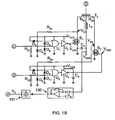
- Output voltage V OUT is compared with reference voltage V R in block 100 (comprising reference V R and an error amplifier with a compensation network) as shown in Fig. 1B.
- the output of block 100 is fed into isolation circuit 101 (usually an opto-coupler or isolation transformer) and error signal V E is fed into controller block 102 which comprises, for example, but is not limited to, a PWM controller, two driver stages generating out-of-phase outputs OUTA and OUTB, and ON/OFF logic.
- Block 102 may also contain additional protection features very often found in converters. However, they are not relevant for the purpose of this description, and are thus omitted.
- Driver outputs OUTA and OUTB are capable of driving two primary side switches simultaneously (Q 10 and Q 30 , and Q 20 and Q 40 ) as well as supplying magnetizing current to drive transformer T 1 . Note that in Fig. 1A the controller and drivers OUTA and OUTB are referenced to -V IN and thus to the input of the converter.
- Winding N 1 has five windings, N 1 to N 5 (Fig. 1A). Their leakage inductances are illustrated explicitly in Fig.lA as external inductances L 1 , L 2 , L 3 , L 4 and L 5 .
- Winding N 5 is driven from block 102 with signals OUTA and OUTB.
- Capacitor C 1 serves as a dc blocking capacitor. Winding N 1 is connected with one end to the source of transistor Q 10 and the second end is connected to the gate of transistor Q 10 via series diode D 10 and resistor R 5 .
- Resistor R 5 is connected in series with diode D 10 in order to dampen oscillations on the gate of Q 10 caused by resonance between leakage inductance L 1 and the input capacitance of transistor Q 10 .
- Transistor Q 1 shown as a p-channel MOSFET, is connected across the gate and source of Q 10 with its gate connected via resistor R 3 to the end of winding N 1 marked with dot polarity.
- Resistor R 10 connected across the gate and source of transistor Q 10 , is used to increase the noise immunity of Q 10 when the voltage across winding N 1 is zero.
- Resistor R 3 is connected in series with the gate of transistor Q 1 in order to dampen any undesirable oscillations caused between the input capacitance of transistor Q 1 and the leakage inductance L 1 of winding N 1 .
- winding N 2 is connected with one end to the source of transistor Q 40 and the second end is connected to the gate of transistor Q 40 via series diode D 40 and resistor R 41 .
- Resistor R 41 is connected in series with diode D 40 in order to dampen oscillations on the gate of transistor Q 40 caused by resonance between leakage inductance L 2 and input capacitance of transistor Q 40 .
- Transistor Q 4 shown as a p-channel MOSFET, is connected across the gate and source of transistor Q 40 with its gate connected via resistor R 9 to the end of winding N 2 without the dot marking.
- Resistor R 40 connected across the gate and source of transistor Q 40 ,is used to increase the noise immunity of Q 40 when the voltage across winding N 2 is zero.
- Resistor R 9 is connected in series with the gate of transistor Q 4 in order to dampen any undesirable oscillations caused between the input capacitance of Q 4 and the leakage inductance L 2 of winding N 2 .
- Winding N 4 is used to drive the two bottom primary switches Q 20 and Q 30 connected to the negative side of the input voltage (-V IN ). Each end of winding N 4 is connected to -V IN with diodes D 50 and D 60 . The end of winding N 4 marked with dot polarity (and also marked as point "A" in Fig. 1A) is connected via a series connection with diode D 30 and resistor R 8 to the gate of transistor Q 30 .
- Transistor Q 3 shown as a p-channel MOSFET, is connected across the gate and source of transistor Q 30 with its gate connected via resistor R 7 to end "A" of winding N 4 .
- Resistor R 8 is connected in series with diode D 30 in order to dampen oscillations on the gate of transistor Q 30 caused by resonance between leakage inductance L 4 and input capacitance of primary switch Q 30 .
- Resistor R 30 connected across the gate and source of transistor Q 30 , is used to increase the noise immunity of Q 30 when the voltage across winding N 4 is zero.
- Resistor R 7 is connected in series with the gate of Q 3 in order to dampen any undesirable oscillations caused between the input capacitance of Q 3 and leakage inductance L 4 of winding N 4 .
- Resistor R 60 is connected in order to keep Q 3 off by connecting its gate to its drain when the voltage on winding N 4 is zero.
- winding N 4 not marked by dot polarity (and also marked as point "B" in Fig. 1A) is connected via a series connection of diode D 20 and resistor R 6 to the gate of transistor Q 20 .
- Resistor R 6 is connected in series with diode D 20 in order to dampen oscillations on the gate of Q 20 caused by resonance between leakage inductance L 4 and the input capacitance of primary switch Q 20 .
- Transistor Q 2 shown as a p-channel MOSFET, is connected across the gate and source of transistor Q 20 with its gate connected via resistor R 4 to end "B" of winding N 4 .
- Resistor R 20 connected across the gate and source of transistor Q 20 , is used to increase noise immunity of Q 20 when the voltage across winding N 4 is zero.
- Resistor R 4 is connected in series with the gate of transistor Q 2 in order to dampen any undesirable oscillations caused between the input capacitance of Q 2 and leakage inductance L 4 of winding N 4 .
- Resistor R 70 is used in order to keep transistor Q 2 off by connecting its gate to its drain when the voltage on winding N 4 is zero.
- Winding N 3 is connected to the drive circuitry for synchronous rectifiers S 1 and S 2 .
- the end of winding N 3 marked by dot polarity (also marked as point “D” in Figs. 1 A and 1B) is connected to one input of logic OR gate U 3 and to one end of resistor R 22 .
- the second end of resistor R 22 is connected to the ground of U 3 .
- the other end of winding N 3 not marked by a dot (also marked as point "C” in Figs. 1A and 1B) is connected to one input of logic OR gate U 1 and to one end of resistor R 21 .
- the second end of resistor R 21 is connected to the ground of U 1 .
- each input of logic gates U 1 and U 3 has protection diodes from ground to input and from input to supply voltage V ccs .
- Capacitor C 4 serves as a bypass capacitor across V CCS . If logic gates without these protection diodes are used, then external diodes need to be added for proper operation of the circuit (diodes D 3 -D 10 are shown as external diodes in Fig. 1B).
- Supply voltage V ccs is usually generated from the windings of main transformer T 2 or from a separate bias circuit from the primary side with proper isolation.
- Drive transformer T 1 can also provide the necessary supply voltage V ccs via winding N 3 and diodes D 5 , D 6 , D 8 and D 11 .
- the second input of logic gate U 1 is connected through resistor R 23 to the drain of synchronous rectifier S 1 , and similarly, the second input of logic gate U 3 is connected through resistor R 24 to the drain of synchronous rectifier S 2 .
- These two inputs provide break-before-make turn-on for both S 1 and S 2 .
- the voltages on the inputs of U 1 and U 3 are clamped to V CCS with diodes D 4 and D 7 , respectively.
- the output of U 1 is connected to the input of inverting driver U 2 , which drives S 1
- the output of U 3 is connected to the input of inverting driver U 4 , which drives S 2 .
- Resistors R 21 and R 22 are used for dampening possible oscillations between leakage inductance L 3 and the input capacitance of logic gates U 1 and U 3 .
- L 1 , L 2 and L 4 are the leakage inductances associated with windings N 1 , N 2 and N 4 , of drive transformer T 1 , respectively.
- These three inductances are purposely made larger than usual in order to delay turn-on of primary switches Q 10 , Q 20 , Q 30 and Q 40 . They are carefully designed to have leakage inductances that are very close in value to further increase the efficiency and simplicity of the circuit. This is relatively easy to do if the transformer windings are formed on a multi-layer printed circuit board (PCB). In addition, repeatability and control in manufacturing are excellent. Typical values for these inductances are approximately 100nH and higher.
- the leakage inductance L 3 of winding N 3 of drive transformer T 1 is not critical since winding N 3 is loaded with a high impedance load (resistors R 2 , and R 22 have a typical value of at least few kOhms), and also taking into consideration the input capacitance of logic gates U 1 and U 3 (5pF-10pF being typical). Thus, inductance L 3 will not have a significant impact on the rising and falling edges of the voltage waveforms across winding N 3 and consequently will not add any additional delay in turning off synchronous rectifiers S 1 and S 2 .
- the leakage inductance L 5 of winding N 5 is designed such that in conjunction with leakage inductances L 1 , L 2 and L 4 , proper delay is achieved in turning on the primary switches.
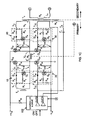
- FIG. 1C An alternative embodiment to the invention illustrated in Fig. 1A is shown in Fig. 1C.
- drive transformer T 3 has four windings.
- Winding N 4 is connected to OUTA and OUTB of controller 102 via series dc blocking capacitor C 1 and has combined the functions of windings N 5 and N 4 from Fig. 1A.
- Two bottom primary side switches, Q 30 and Q 20 are driven from OUTA and OUTB via series inductors L 30 and L 20 , respectively.
- External inductors L 20 and L 30 have the same value for leakage inductance as L 4 from Fig. 1A.
- the rest of the circuitry is the same as in Fig. 1A.
- the drive transformer is simpler with only four windings versus five.
- two extra components, inductances L 20 and L 30 are needed.
- the drive transformer T 1 from Fig. 1A may be preferable since it eliminates the need for inductances L 20 and L 30 , and their associated cost and space on the PCB. Operations of the Figs. 1A and 1C circuits are very similar.
- OUTA (of the controller, for example PWM type) becomes high, while OUTB is low.
- the voltage across all windings of T 1 is positive. Note that the dot polarity next to one end of the windings of the transformer is used for reference and is now positive with respect to other side of the windings.
- the voltage across winding N 3 is positive and the end of winding N 3 connected to the input of U 1 (marked as point "C" in Fig. 1B) is clamped with an internal diode (shown as external diode D 6 ) to the negative voltage equal to the forward voltage drop of the diode.
- the body diode of transistor Q 2 clamps a negative voltage across primary switch Q 20 to near zero during time DT s /2, while D 20 is reverse biased.
- the body diode of transistor Q 4 clamps negative voltage across Q 40 to near zero during time DT s /2, while D 40 is reverse biased. Clamping negative voltage on transistors Q 20 and Q 40 during off time is preferred in order to reduce gate drive losses.
- the voltage across the windings of transformer T 2 is positive and output inductor current is supplied from input to output through winding N S1 .
- the voltage across S 2 is also positive.
- the current in output inductor L 0 splits between synchronous rectifier S 1 and the body diode of synchronous rectifier S 2 , which as a consequence, has shorted windings of transformer T 2 .
- the output of U 3 goes low (since the input connected to winding N 3 is zero), and the output of U 4 goes high and synchronous rectifier S 2 is turned-on (time interval t d2 ).
- Both S 1 and S 2 are on during the rest of the half of the switching period and the voltages across the windings of T 1 and T 2 are zero (time interval t x ).
- winding N 4 marked as point "A” is connected to -V IN via diode D 60 .
- the body diode of Q 1 clamps a negative voltage across Q 10 to near zero during time DT s /2, while diode D 10 is reverse biased.
- the body diode of Q 3 clamps negative voltage across Q 30 to near zero during time DT s /2, while D 30 is reverse biased. Clamping a negative voltage on Q 10 and Q 30 during off time is desirable in order to reduce gate drive losses.
- time DT s /2 - t d3 the voltage across the windings of transformer T 2 is negative and the output inductor current is supplied from input through winding N S2 .
- the voltage across synchronous rectifier S 1 is positive.
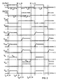
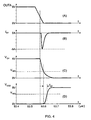
- the turn-on waveforms of primary switch Q 10 are shown in more detail in Fig. 3 for two different values of leakage inductance L 1 , L 1(1) and L 1(2) , in order to explain the turn-on delay of primary switch Q 10 due to the finite rise time of the current in leakage inductance L 1 of winding N 1 . It is assumed that there is no overshoot in gate voltage. Note that the other three primary switches, Q 20 , Q 30 and Q 40 have the same gate drive waveforms.
- L 1(2) The lower value of leakage inductance L 1 , denoted L 1(2) , allows a higher peak current for charging the input capacitance of Q 10 and consequently it allows for a faster turn-on of Q 10 and shorter delay between turning-off of S 2 and tuming-on of Q 10 .
- voltage level V ON in waveform (C) in Fig. 3 represents the voltage level of V G10 at which Q 10 is fully on, and t d1 (either t d1(1) or t d1(2) ) is the so called “dead time" and represents time during which both synchronous rectifier S 2 and primary switch Q 10 are off.
- Dead time is necessary in order to avoid cross conduction of synchronous rectifier S 2 and primary switch Q 10 and Q 30 (and S 1 and Q 20 and Q 40 ).
- Dead time, t d1 (equivalently, t d2 )
- the body diode of S 2 (equivalently, S 1 ) is carrying half of the output inductor current, thus decreasing efficiency of the converter.
- the dead time is too short, that is Q 10 and Q 30 are turned-on before S 2 is turned-off, there will be cross-conduction that would result in efficiency drop. Therefore, it is important to have well-controlled dead times in order to have the highest efficiency. With proper design of leakage inductances and repeatability in manufacturing, dead time is optimized for highest efficiency.
- the turn-off waveforms for primary switch Q 10 are shown in more detail in Fig. 4. Since diode D 10 becomes reverse biased when OUTA goes low, the discharging current of the input capacitance of Q 10 is going through transistor Q 1 and is limited, in first approximation, only by the ON resistance and turn-on characteristic of Q 1 , but not affected by leakage inductance L 1 . The presence of leakage inductance is desirable during the turn-off transient since the leakage inductance generates a negative spike, which improves the turn-on of Q 1 .
- winding N 5 (from the Fig. 1A embodiment) is not needed, as shown in Figs. 5A and 5B.
- OUTA and OUTB are generated from controller 104 referenced to the output side of the converter and are directly connected to one input of logic gates U 3 and U 1 .
- Winding N 3 is connected via dc blocking capacitor C 3 to the inputs of the two inverting drivers DRIVER_A and DRIVER_B which are controlled by OUTA and OUTB, respectively.
- the salient waveforms shown in Fig. 2 are still valid for the circuit in Figs. 5A and 5B.
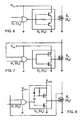
- Figs. 6, 7 and 8 Illustrated in Figs. 6, 7 and 8 are partial circuitry embodiments for possible realization of drivers U 2 and U 4 .
- logic gate U 1 (U 3 ) is a NOR gate instead of an OR gate since driver stage U 2 (U 4 ) is non-inverting.
- the drivers operate the same way so only U 2 (and not U 4 ) is shown.
- driver stage U 2 (U 4 ) is inverting and logic gate U 1 (U 3 ) is an OR gate as in Figs. 1 B and 5B.
- driver stage U 2 (U 4 ) allows synchronous rectifier S 1 (S 2 ) to be driven with a voltage higher than the supply voltage for logic gate U 1 (U 3 ).
- Practical realizations of drivers U 2 and U 4 different from those in Figs. 6, 7 and 8, are also possible.
- transistors Q 1 through Q 4 are shown as p-channel MOSFETs, it is possible to use n-channel MOSFETs instead, as well as bipolar transistors. The former are more practical due to an easier drive and an integrated body diode, which would be needed as an external component if Q 1 through Q 4 were bipolar transistors.
- One possible realization using n-channel MOSFETs as Q 1 and Q 4 for example from Figs. 1A, 1C and 5A is shown in Figs. 9A and 9B.
- two additional diodes, D 70 and D 80 are used as shown in Figs. 10A and 10B.
- Diodes D 70 and D 80 prevent windings N 1 and N 2 from shorting via the collector-emitter junction of Q 1 and Q 4 , respectively.
- One possible realization using p-n-p transistors for Q 2 and Q 3 is shown in Figs. 10C and 10D. Since diodes D 50 and D 60 already exist (Figs. 1A and 5A), extra diodes are not needed as was the case in Figs. 10A and 10B.
- control circuit is referenced to the input side of the converter, as is controller 102 in Fig. 1A, there must be means to disable the converter from a condition sensed on the output side, for example, in case of output over-voltage, under-voltage or over-current conditions.
- feedback and control circuit is referenced to the output of the converter, as is controller 104 in Fig. 5B, there must be means to disable the converter from the input side of converter, for example, in case of input over-voltage, under-voltage conditions or in order to turn the converter off.
- a previous solution which has been employed uses an opto-coupler. This solution has several disadvantages:
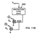
- FIG. 11 A and 11B An alternate solution disclosed herein provides, as shown in Figs. 11 A and 11B, means for disabling the control circuit on the input side from a condition sensed on the output side of the converter, as described in detail below.
- the principle idea is to short winding N 3 of drive transformer T 3 , detect excessive current in winding N 5 due to shorted winding N 3 , and disable the control circuit and drivers OUTA and OUTB (controller 102 in Fig. 11A), thus resulting in turn-off the converter.
- Different circuit realizations are possible as is known to one of ordinary skill in the art. Protection logic 200 (Fig.
- comparator U 6 that has a threshold set such that in normal operation the voltage drop across resistor R 12 will not trip U 6 , but when winding N 3 is shorted, comparator U 6 is tripped, and generates signal DSB which disables controller 102 and both OUTA and OUTB are disabled (that is, they are in the low state).
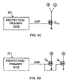
- An alternate embodiment disclosed herein provides, as shown in Figs. 5A through D, a means for disabling the control circuit referenced to the output side of the converter from a condition sensed on the input side of converter as described in detail below.
- Protection logic 201 on the input side of the converter shown in Figs. 5C and 5D, initially senses a fault condition on the input side and generates a disable signal DSP that is active (high).
- Switch Q 100 shown as an n-channel MOSFET as one possible practical realization in Fig. 5C, is connected to one end (either at point "A" or "B") of winding N 4 (Fig. 5A).
- transistor Q 100 In response to an active disable signal DSP, transistor Q 100 is turned-on and winding N 4 is shorted via Q 100 and diode D 60 , if Q 100 is connected to end "A" of N 4 . Similarly, winding N 4 is shorted via transistor Q 100 and diode D 50 if Q 100 is connected to end "B" of N 4 .
- two primary side switches (specifically Q 20 and Q 30 ), that were on before the DSP signal became active, are turned-off.
- increased current in winding N 3 is sensed with resistor R 11 connected between supply voltage V ccs and drivers DRIVER_A and DRIVER_B referenced to the output of the converter.
- DRIVER_A and DRIVER_B are shown in Fig. 5B explicitly with a possible realization as complementary pairs of p- and n-channel MOSFETs.
- the voltage across resistor R 11 is sensed with comparator U 5 that has a threshold set such that in normal operation the voltage drop across resistor R 11 will not trip U 5 , but when winding N 4 is shorted, comparator U 5 is activated, causing controller 104 to disable OUTA and OUTB, and consequently the converter.
- switch Q 100 can be connected in parallel with either primary switch Q 20 or Q 30 in which case the gate of transistor Q 20 or Q 30 will be shorted in response to the active disable signal.
- winding N 4 will be shorted via transistor Q 100 and diodes D 20 and D 60 or diodes D 30 and D 50 , causing again increased current through windings N 4 and N 3 .
- a possible drawback of this solution is that the capacitance of transistor Q 100 may affect the turn-on performance of primary switches Q 20 or Q 30 .
- leakage inductance L 4 is needed to be less then L 1 or L 2 , thus resulting in a more complicated drive transformer design.
- the disable circuit from Fig. 5C has an inherent delay of one switching period since winding N 4 is shorted only during the on-time of either transistors Q 10 and Q 10 or transistors Q 20 and Q 40 . In most applications this should not be a problem.
- two switches shown as n-channel MOSFETs Q 5 and Q 6 in Fig. 5D are used to short winding N 4 when the DSP signal is high in order to stop controller 104 and disable OUTA and OUTB, immediately, whenever a fault condition on the input side of converter is detected.
- the body diodes of Q 5 and Q 6 can replace diodes D 50 and D 60 , respectively, thus further simplifying the circuit.
- this circuit provides an inherent delay of one half of the switching period.
- winding N 4 has the best coupling with winding N 3 , while windings N 2 and N 1 are placed in layers above and below in the PCB. This is the preferred structure because it provides enough leakage between N 3 and N 1 and N 2 , and also decouples N 1 and N 2 from N 3 when N 4 is shorted. Other arrangements of windings in the drive transformer embodiments are also possible.
Landscapes
- Engineering & Computer Science (AREA)
- Power Engineering (AREA)
- Dc-Dc Converters (AREA)
- Power Conversion In General (AREA)
- Control Of Motors That Do Not Use Commutators (AREA)
- Cookers (AREA)
Claims (30)
- Schaltspannungswandler zum Umwandeln einer Eingangsspannung (VIN) von einer Eingangsquelle in eine Ausgangsspannung (VOUT) zur Versorgung einer Last, aufweisend:einen Spannungsisolationstransformator (T2) mit einer Primärwicklung (NP) und einer zweiten Sekundärwicklung (NS1, NS2),eine primäre Wandlerschaltung in Vollbrückenanordnung mit einem ersten und einem zweiten primären steuerbaren Leistungsschalter (Q10, Q20), die einen Zweig der Vollbrücke bilden, und einem dritten und einem vierten primären steuerbaren Leistungsschalter (Q30, Q40), die einen zweiten Zweig der Vollbrücke bilden, wobei der erste und der vierte primäre steuerbare Leistungsschalter mit der positiven Seite der Eingangsspannung und der zweite und der dritte primäre steuerbare Leistungsschalter mit der negativen Seite der Eingangsspannung verbunden sind und die Zweige der Vollbrücke jeweils mit der Primärwicklung des Spannungstransformators verbunden sind, um die Eingangsspannung wechselweise der Primärwicklung des Spannungsisolationstransformators zuzuführen und in der Primärwicklung einen im wesentlichen symmetrischen Strom zu erzeugen,eine sekundäre Vollwellen-Wandlerschaltung, die von der primären Wandlerschaltung völlig isoliert ist und einen ersten und einen zweiten Synchrongleichrichter (S1, S2) aufweist, die einzeln schaltbar sind und jeweils zwischen ein entsprechendes Ende der ersten und der zweiten Sekundärwicklung und die Last geschaltet sind,eine erste, eine zweite, eine dritte und eine vierte primäre Schaltersteuerschaltung (10, 20, 30, 40) zum Steuern des Leitens des ersten, des zweiten, des dritten und des vierten primären steuerbaren Leistungsschalters,eine Synchrongleichrichtersteuerschaltung (D3-D11, R21-R24, U1-U4) zum Steuern des Leitens jeweils des ersten und des zweiten Synchrongleichrichters,eine Schalterleitungssteuerschaltung (102) mit zwei Ausgängen (OUTA, OUTB) mit um etwa 180 Grad verschobenen, im wesentlichen symmetrischen Wellenformen, um das Leiten der primären steuerbaren Leistungsschalter und des ersten und des zweiten Synchrongleichrichters zu steuern, undeinen Treibertransformator (T1), um die notwendigen Verzögerungen zwischen dem jeweiligen Leiten der primären steuerbaren Leistungsschalter und dem ersten und dem zweiten Synchrongleichrichter zu bewirken sowie Spannung zur Steuerung der primären steuerbaren Leistungsschalter und des ersten und des zweiten Synchrongleichrichters zu liefern, wobei der Treibertransformator eine Isolation zwischen den primären Schaltersteuerschaltungen und den Synchrongleichrichtersteuerschaltungen bewirkt, wobei die Synchrongleichrichtersteuerschaltung während eines Teils der Schaltperiode, wenn die Spannung über den Wicklungen des Treibertransformators Null ist und so dass die Spannung über den Wicklungen des Spannungsisolationstransformators Null wird, sowohl den ersten als auch den zweiten Synchrongleichrichter einschaltet, und wobei der Treibertransformator folgendes aufweist:eine mit der Schalterleitungssteuerschaltung verbundene erste Treibertransformatorwicklung (N5),eine mit der ersten primären Schaltersteuerschaltung verbundene zweite Treibertransformatorwicklung (N1) zum Steuern des Leitens des ersten primären steuerbaren Leistungsschalters, undeine mit der vierten primären Schaltersteuerschaltung verbundene dritte Treibertransformatorwicklung (N2) zum Steuern des Leitens des vierten primären steuerbaren Leistungsschalters.
- Spannungswandler nach Anspruch 1 mit einer vierten Treibertransformatorwicklung (N3), die mit den Synchrongleichrichtersteuerschaltungen verbunden ist und das Leiten des Synchrongleichrichters steuert.
- Spannungswandler nach Anspruch 1, wobei die Schalterleitungssteuerschaltung auch mit einer Seite der Eingangsspannung verbunden ist.
- Spannungswandler nach Anspruch 3, wobei die zweite und die dritte Treibertransformatorwicklung außerdem Streuinduktivitäten aufweisen, die den Treibertransformatorwicklungen zugeordnet sind, wobei ein Viertel der Schwingungsperiode, die von der Eingangskapazität des pimären Schalters und der Streuinduktivität verursacht wird, länger als die Abschaltzeit des Synchrongleichrichters ist, so dass ein Einschalten der primären Schalter um die Zeitspanne verzögert ist, die benötigt wird, um die Synchrongleichrichter abzuschalten, um ein Querleiten zu verhindern.
- Spannungswandler nach Anspruch 1, wobei die zweite und die dritte primäre Schaltersteuerung über eine erste und eine zweite Induktivität (L20, L40) mit der Schalterleitungssteuerschaltung verbunden sind, wobei die erste und die zweite Induktivität so ausgewählt sind, dass ihre Induktivitäten nahe den Streuinduktivitäten liegen, die der zweiten und der dritten Treibertransformatorwicklung zugeordnet sind.
- Spannungswandler nach Anspruch 2, mit einer fünften Treibertransformatorwicklung (N4), die mit der zweiten und der dritten primären Schaltersteuerungsschaltung verbunden ist, wobei die fünfte Treibertransformatorwicklung eine Streuinduktivität (L4) für eine optimale Verzögerung beim Einschalten des zweiten und des dritten primären steuerbaren Leistungsschalters aufweist und die der fünften Treibertransformatorwicklung zugeordnete Induktivität so gewählt ist, dass sie zu den Streuinduktivitäten der zweiten und der dritten Treibertransformatorwicklung passt.
- Spannungswandler nach Anspruch 1, wobei die primären Schaltersteuerschaltungen außerdem jeweils Folgendes aufweisen:mindestens einen steuerbaren Schalter (Q1-Q4), der über die Steueranschlüsse des primären steuerbaren Leistungsschalters geschaltet ist und eingerichtet ist, den primären steuerbaren Leistungsschalter wirksam zu steuern und sein Abschalten ausreichend schnell zu bewirken, damit ein Querleiten der primären steuerbaren Leistungsschalter im Fall nahezu gleicher Leitfähigkeitszeiten vermieden wird, undeine Diode (D10, D20, D30, D40) zum Steuern und Einschalten des primären steuerbaren Leistungsschalters und zum Steuern und Einschalten des steuerbaren Schalters.
- Spannungswandler nach Anspruch 7, wobei der mindestens eine steuerbare Schalter physisch nahe am ersten und am zweiten primären steuerbaren Leistungsschalter angeordnet ist, so dass sich die Abschaltzeit der primären Schalter nicht wesentlich verringern würde, wenn der mindestens eine steuerbare Schalter näher an den ersten und den zweiten primären steuerbaren Leistungsschalter heranbewegt würde.
- Spannungswandler nach Anspruch 2, wobei die Synchrongleichrichtersteuerschaltungen jeweils Folgendes aufweisen:mindestens eine logische Doppeleingangsschaltung (U1-U4) zum Steuern des Leitens des jeweiligen Synchrongleichrichters mit relativ kleiner Eingangskapazität, so dass die Streuinduktivität der vierten Transformatorwicklung die Verzögerung beim Abschalten des Synchrongleichrichters nicht nachteilig beeinflusst, wobei ein Eingang der logischen Doppeleingangsschaltung mit einem Ende der mit der Synchrongleichrichtersteuerschaltung verbundenen Treibertransformatorwicklung und der zweite Eingang der logischen Doppeleingangsschaltung mit dem entsprechenden Synchrongleichrichter verbunden ist, um ein Einschalten des Synchrongleichrichters zu verhindern, bevor die Spannung über ihm auf einen vorbestimmten Wert fällt, undeine mit dem jeweiligen Synchrongleichrichter verbundene Treiberschaltung zum optimalen Einschalten des Synchrongleichrichters und zum optimalen Ausschalten des Synchrongleichrichters mit minimaler Verzögerung.
- Spannungswandler nach Anspruch 9, wobei die logische Doppeleingangsschaltung an jedem der beiden Eingänge Schutzdioden (D3-D11) aufweist, um wahlweise eine negative und eine positive Spannung, die größer als die Versorgungsspannung sind, zum Anlegen über den jeweiligen Eingang der logischen Doppeleingangsschaltung liefern zu können.
- Spannungswandler nach Anspruch 10, wobei die logische Doppeleingangsschaltung an jedem der beiden Eingänge Serienwiderstände (R21-R24) aufweist, um den Strom in den Schutzdioden zu begrenzen, wann immer eine negative oder positive Spannung, die größer als die Versorgungsspannung ist, über den jeweiligen Eingang der logischen Doppeleingangsschaltung angelegt wird.
- Spannungswandler nach Anspruch 2, mit einer Bezugsschaltung (100), um einen Bezug der Schalterleitungssteuerschaltung auf die Ausgabe des Spannungsisolationstransformators herzustellen.
- Spannungswandler nach Anspruch 3, mit einer Einrichtung zum Sperren des Spannungswandlers auf der Eingangsseite und somit auf der Ausgangsseite von einer auf der Ausgangsseite erfassten Bedingung.
- Spannungswandler nach Anspruch 3, mit einer Einrichtung zum Freigeben der Spannungswandlung auf der Eingangsseite von einer auf der Ausgangsseite erfassten Bedingung.
- Spannungswandler nach Anspruch 12, mit einer Einrichtung zum Sperren des Schaltspannungswandlers von seinem Ausgang her aufgrund einer auf seiner Eingangsseite erfassten Bedingung.
- Verfahren zum Betrieb eines Schaltspannungswandlers zum Umwandeln einer Eingangsspannung (VIN) von einer Eingangsquelle in eine Ausgangsspannung (VOUT) zur Lieferung an eine Last, wobei:ein Spannungsisolationstransformators (T2) mit einer Primärwicklung (NP) und einer Sekundärwicklung (NS1, NS2) betrieben wird,eine primäre Wandlerschaltung in Vollbrückenanordnung mit einem ersten und einem zweiten primären steuerbaren Leistungsschalter (Q10, Q20), die einen Zweig der Vollbrücke bilden, und einem dritten und einem vierten primären steuerbaren Leistungsschalter (Q30, Q40), die einen zweiten Zweig der Vollbrücke bilden, betrieben wird, wobei der erste und der vierte primäre steuerbare Leistungsschalter mit der positiven Seite der Eingangsspannung und der zweite und der dritte primäre steuerbare Leistungsschalter mit der negativen Seite der Eingangsspannung verbunden sind und die Zweige der Vollbrücke jeweils mit der Primärwicklung des Spannungstransformators verbunden sind und die Eingangsspannung wechselweise der Primärwicklung des Spannungsisolationstransformators zuführen, um in der Primärwicklung einen im wesentliche symmetrischen Strom zu erzeugen,eine sekundäre Vollwellengleichrichtung vorgesehen wird, die von der primären Wandlerschaltung völlig isoliert ist und einen ersten und einen zweiten Synchrongleichrichter (S1, S2) aufweist, die einzeln schaltbar sind und jeweils zwischen ein entsprechendes Ende der ersten und der zweiten Sekundärwicklung und die Last geschaltet sind,eine erste, eine zweite, eine dritte und eine vierte primäre Schaltersteuerschaltung (10, 20, 30, 40) das Leiten des ersten, des zweiten, des dritten und des vierten primären steuerbaren Leistungsschalters steuert,eine Synchrongleichrichtersteuerschaltung (D3-D11, R21-R24' U1-U4) das Leiten des jeweiligen ersten und zweiten Synchrongleichrichters steuert,eine Schalterleitungssteuerschaltung (102) mit zwei Ausgängen (OUTA, OUTB) mit im wesentlichen symmetrischen, um etwa 180 Grad verschobenen Wellenformen das Leiten der primären steuerbaren Leistungsschalter und des ersten und des zweiten Synchrongleichrichters steuert, undein Treibertransformator (T1) notwendige Verzögerungen zwischen dem jeweiligen Leiten der primären steuerbaren Leistungsschalter und des ersten und des zweiten Synchrongleichrichters bewirkt sowie eine Spannung zum Steuern der primären steuerbaren Leistungsschalter und des ersten und des zweiten Synchrongleichrichters liefert und eine Isolation zwischen den primären Schaltersteuerschaltungen und den Synchrongleichrichtersteuerschaltungen bewirkt, wobei die Synchrongleichrichtersteuerschaltung während eines Teils der Schaltperiode, wenn die Spannung über den Wicklungen des Treibertransformators Null ist und so dass die Spannung über den Wicklungen des Spannungsisolationstransformators Null wird, sowohl den ersten als auch den zweiten Synchrongleichrichter einschaltet, wobei der Treibertransformator Folgendes umfasst:eine erste Treibertransformatorwicklung (N5), die mit der Schalterleitungssteuerschaltung verbunden ist,eine zweite Treibertransformatorwicklung (N1), die mit der ersten primären Schaltersteuerschaltung verbunden ist und das Leiten des ersten primären steuerbaren Leistungsschalters steuert, undeine dritte Treibertransformatorwicklung (N2), die mit der vierten primären Schaltersteuerschaltung verbunden ist und das Leiten des vierten primären steuerbaren Leistungschalters steuert.
- Verfahren nach Anspruch 16 mit einer vierten Treibertransformatorwicklung (N3), die mit den Synchrongleichrichtersteuerschaltungen verbunden ist und das Leiten des Synchrongleichrichters steuert.
- Verfahren nach Anspruch 16, wobei die Schaltersteuerschaltung außerdem mit einer Seite der Eingangsspannung verbunden ist.
- Verfahren nach Anspruch 18, wobei die zweite und die dritte Treibertransformatorwicklung außerdem Streuinduktivitäten aufweisen, die den Treibertransformatorwicklungen zugeordnet sind, wobei ein Viertel der Schwingungsperiode, die von der Eingangskapazität des primären Schalters und der Streuinduktivität verursacht wird, länger als die Abschaltzeit des Synchrongleichrichters ist, so dass ein Einschalten der primären Schalter um die Zeitspanne verzögert wird, die benötigt wird, um die Synchrongleichrichter abzuschalten, um ein Querleiten zu verhindern.
- Verfahren nach Anspruch 16, wobei die zweite und die dritte primäre Schaltersteuerung über eine erste und eine zweite Induktivität (L20, L40) mit der Schalterleitungssteuerschaltung verbunden sind, wobei die erste und die zweite Induktivität so ausgewählt sind, dass ihre Induktivitäten nahe den Streuinduktivitäten liegen, die der zweiten und der dritten Treibertransformatorwicklung zugeordnet sind.
- Verfahren nach Anspruch 17, mit einer fünften Treibertransformatorwicklung (N4), die mit der zweiten und der dritten primären Schaltersteuerungsschaltung verbunden ist, wobei die fünfte Treibertransformatorwicklung eine Streuinduktivität (L4) für eine optimale Verzögerung beim Einschalten des zweiten und des dritten primären steuerbaren Leistungsschalters aufweist und die der fünften Treibertransformatorwicklung zugeordnete Induktivität so gewählt ist, dass sie zu den Streuinduktivitäten der zweiten und der dritten Treibertransformatorwicklung passt.
- Verfahren nach Anspruch 16, wobei die primären Schaltersteuerschaltungen außerdem jeweils Folgendes aufweisen:mindestens einen steuerbaren Schalter (Q1-Q4), der über die Steueranschlüsse des primären steuerbaren Leistungsschalters geschaltet ist und so eingerichtet ist, den primären steuerbaren Leistungsschalter wirksam zu steuern und sein Abschalten ausreichend schnell zu bewirken, damit ein Querleiten der primären steuerbaren Leistungsschalter im Fall nahezu gleicher Leitfähigkeitszeiten vermieden wird, undeine Diode (D10, D20, D30, D40) zum Steuern und Einschalten des primären steuerbaren Leistungsschalters und zum Steuern und Einschalten des steuerbaren Schalters.
- Verfahren nach Anspruch 22, wobei der mindestens eine steuerbare Schalter physisch nahe am ersten und am zweiten primären steuerbaren Leistungsschalter angeordnet ist, so dass sich die Abschaltzeit der primären Schalter nicht wesentlich verringern würde, wenn der mindestens eine steuerbare Schalter näher an den ersten und den zweiten primären steuerbaren Leistungsschalter heranbewegt würde.
- Verfahren nach Anspruch 17, wobei die Synchrongleichrichtersteuerschaltungen jeweils Folgendes aufweisen:mindestens eine logische Doppeleingangsschaltung (U1-U4) zum Steuern des Leitens des jeweiligen Synchrongleichrichters mit relativ kleiner Eingangskapazität, so dass die Streuinduktivität der vierten Transformatorwicklung die Verzögerung beim Abschalten des Synchrongleichrichters nicht nachteilig beeinflusst, wobei ein Eingang der logischen Doppeleingangsschaltung mit einem Ende der mit der Synchrongleichrichtersteuerschaltung verbundenen Treibertransformatorwicklung und der zweite Eingang der logischen Doppeleingangsschaltung mit dem entsprechenden Synchrongleichrichter verbunden ist, um ein Einschalten des Synchrongleichrichters zu verhindern, bevor die Spannung über ihm auf einen vorbestimmten Wert fällt, undeine mit dem jeweiligen Synchrongleichrichter verbundene Treiberschaltung, die für optimales Einschalten des Synchrongleichrichters und optimales Ausschalten des Synchrongleichrichters mit minimaler Verzögerung sorgt.
- Verfahren nach Anspruch 24, wobei die logische Doppeleingangsschaltung an jedem der beiden Eingänge Schutzdioden (D3-D11) aufweist, um wahlweise eine negative und eine positive Spannung, die größer als die Versorgungsspannung sind, zum Anlegen über den jeweiligen Eingang der logischen Doppeleingangsschaltung liefern zu können.
- Verfahren nach Anspruch 25, wobei die logische Doppeleingangsschaltung an jedem der beiden Eingänge Serienwiderstände (R21-R24) aufweist, um den Strom in den Schutzdioden zu begrenzen, wann immer eine negative oder positive Spannung, die größer als die Versorgungsspannung ist, über den jeweiligen Eingang der logischen Doppeleingangsschaltung angelegt wird.
- Verfahren nach Anspruch 17, mit einer Bezugsschaltung (100), die einen Bezug der Schalterleitungssteuerschaltung auf die Ausgabe des Spannungsisolationstransformators herstellt.
- Verfahren nach Anspruch 18, wobei der Spannungswandler von einer auf der Ausgangsseite erfassten Bedingung auf der Eingangsseite und somit auf der Ausgangsseite gesperrt wird.
- Verfahren nach Anspruch 18, wobei der Spannungswandler von einer auf der Ausgangsseite erfassten Bedingung auf der Eingangsseite freigegeben wird.
- Verfahren nach Anspruch 27, wobei der Schaltspannungswandler aufgrund einer auf seiner Eingangsseite erfassten Bedingung von seinem Ausgang her gesperrt wird.
Applications Claiming Priority (5)
| Application Number | Priority Date | Filing Date | Title |
|---|---|---|---|
| US26571401P | 2001-02-01 | 2001-02-01 | |
| US265174P | 2001-02-01 | ||
| US61189 | 2002-02-01 | ||
| PCT/US2002/002779 WO2002061927A2 (en) | 2001-02-01 | 2002-02-01 | Isolated drive circuitry used in switch-mode power converters |
| US10/061,189 US6804125B2 (en) | 2001-02-01 | 2002-02-01 | Isolated drive circuitry used in switch-mode power converters |
Publications (2)
| Publication Number | Publication Date |
|---|---|
| EP1405394A2 EP1405394A2 (de) | 2004-04-07 |
| EP1405394B1 true EP1405394B1 (de) | 2007-12-12 |
Family
ID=31996451
Family Applications (2)
| Application Number | Title | Priority Date | Filing Date |
|---|---|---|---|
| EP02714806A Expired - Lifetime EP1356575B1 (de) | 2001-02-01 | 2002-02-01 | Isolierte treiberschaltungsanordnung zur verwendung in leistungsschaltreglern |
| EP02709247A Expired - Lifetime EP1405394B1 (de) | 2001-02-01 | 2002-02-01 | Isolierte treiberschaltungsanordnung zur verwendung in leistungsschaltreglern |
Family Applications Before (1)
| Application Number | Title | Priority Date | Filing Date |
|---|---|---|---|
| EP02714806A Expired - Lifetime EP1356575B1 (de) | 2001-02-01 | 2002-02-01 | Isolierte treiberschaltungsanordnung zur verwendung in leistungsschaltreglern |
Country Status (7)
| Country | Link |
|---|---|
| US (2) | US6804125B2 (de) |
| EP (2) | EP1356575B1 (de) |
| JP (2) | JP2004521588A (de) |
| AT (2) | ATE361579T1 (de) |
| AU (2) | AU2002243742A1 (de) |
| DE (2) | DE60219886D1 (de) |
| WO (2) | WO2002061927A2 (de) |
Families Citing this family (49)
| Publication number | Priority date | Publication date | Assignee | Title |
|---|---|---|---|---|
| US7269034B2 (en) | 1997-01-24 | 2007-09-11 | Synqor, Inc. | High efficiency power converter |
| US5999417A (en) * | 1997-01-24 | 1999-12-07 | Fische, Llc | High efficiency power converter |
| DE10161743B4 (de) * | 2001-12-15 | 2004-08-05 | Hüttinger Elektronik GmbH & Co. KG | Hochfrequenzanregungsanordnung |
| US7280026B2 (en) | 2002-04-18 | 2007-10-09 | Coldwatt, Inc. | Extended E matrix integrated magnetics (MIM) core |
| TWI271023B (en) * | 2003-08-21 | 2007-01-11 | Sony Corp | Switching power-supply circuit |
| US6970023B2 (en) * | 2003-12-17 | 2005-11-29 | Texas Instruments Incorporated | Modulated transistor gate driver with planar pulse transformer |
| US6906931B1 (en) * | 2004-01-30 | 2005-06-14 | Astec International Limited | Zero-voltage switching half-bridge DC-DC converter topology by utilizing the transformer leakage inductance trapped energy |
| US7116563B2 (en) * | 2004-05-19 | 2006-10-03 | Semtech Corporation | Dual mode over-current protection for switching mode power converter |
| US7355867B2 (en) * | 2004-08-17 | 2008-04-08 | Elster Electricity, Llc | Power supply for an electric meter having a high-voltage regulator that limits the voltage applied to certain components below the normal operating input voltage |
| US20070211500A1 (en) * | 2006-03-02 | 2007-09-13 | Hipro Electronic Co., Ltd | DC-DC converter with direct driven synchronous rectifier |
| US9197132B2 (en) | 2006-12-01 | 2015-11-24 | Flextronics International Usa, Inc. | Power converter with an adaptive controller and method of operating the same |
| US7675759B2 (en) | 2006-12-01 | 2010-03-09 | Flextronics International Usa, Inc. | Power system with power converters having an adaptive controller |
| US7468649B2 (en) | 2007-03-14 | 2008-12-23 | Flextronics International Usa, Inc. | Isolated power converter |
| US8526206B2 (en) * | 2007-07-09 | 2013-09-03 | Power Concepts Nz Limited | Drive circuit |
| DE112007003667A5 (de) * | 2007-07-23 | 2010-07-01 | Hüttinger Elektronik GmbH & Co. KG | Plasmaversorgungseinrichtung |
| CN102217181B (zh) | 2008-11-14 | 2014-09-03 | 伟创力国际美国公司 | 用于同步整流器的驱动器以及采用该驱动器的功率转换器 |
| DE102008055157A1 (de) * | 2008-12-23 | 2010-06-24 | Infineon Technologies Ag | Ansteuerschaltung für eine Leistungshalbleiteranordnung und Leistungshalbleiteranordnung |
| US9088216B2 (en) | 2009-01-19 | 2015-07-21 | Power Systems Technologies, Ltd. | Controller for a synchronous rectifier switch |
| CN102342007B (zh) | 2009-01-19 | 2015-01-07 | 伟创力国际美国公司 | 用于功率转换器的控制器 |
| US9019061B2 (en) | 2009-03-31 | 2015-04-28 | Power Systems Technologies, Ltd. | Magnetic device formed with U-shaped core pieces and power converter employing the same |
| US8643222B2 (en) | 2009-06-17 | 2014-02-04 | Power Systems Technologies Ltd | Power adapter employing a power reducer |
| US9077248B2 (en) | 2009-06-17 | 2015-07-07 | Power Systems Technologies Ltd | Start-up circuit for a power adapter |
| US8514593B2 (en) | 2009-06-17 | 2013-08-20 | Power Systems Technologies, Ltd. | Power converter employing a variable switching frequency and a magnetic device with a non-uniform gap |
| US8638578B2 (en) | 2009-08-14 | 2014-01-28 | Power System Technologies, Ltd. | Power converter including a charge pump employable in a power adapter |
| US8976549B2 (en) | 2009-12-03 | 2015-03-10 | Power Systems Technologies, Ltd. | Startup circuit including first and second Schmitt triggers and power converter employing the same |
| US8520420B2 (en) | 2009-12-18 | 2013-08-27 | Power Systems Technologies, Ltd. | Controller for modifying dead time between switches in a power converter |
| US9246391B2 (en) | 2010-01-22 | 2016-01-26 | Power Systems Technologies Ltd. | Controller for providing a corrected signal to a sensed peak current through a circuit element of a power converter |
| US8787043B2 (en) | 2010-01-22 | 2014-07-22 | Power Systems Technologies, Ltd. | Controller for a power converter and method of operating the same |
| US8767418B2 (en) | 2010-03-17 | 2014-07-01 | Power Systems Technologies Ltd. | Control system for a power converter and method of operating the same |
| US8687386B2 (en) * | 2010-12-06 | 2014-04-01 | The Boeing Company | Synchronous rectifier bi-directional current sensor |
| US8929103B2 (en) | 2011-03-23 | 2015-01-06 | Pai Capital Llc | Integrated magnetics with isolated drive circuit |
| US8792257B2 (en) | 2011-03-25 | 2014-07-29 | Power Systems Technologies, Ltd. | Power converter with reduced power dissipation |
| US8792256B2 (en) | 2012-01-27 | 2014-07-29 | Power Systems Technologies Ltd. | Controller for a switch and method of operating the same |
| US9190898B2 (en) | 2012-07-06 | 2015-11-17 | Power Systems Technologies, Ltd | Controller for a power converter and method of operating the same |
| US9214264B2 (en) | 2012-07-16 | 2015-12-15 | Power Systems Technologies, Ltd. | Magnetic device and power converter employing the same |
| US9099232B2 (en) | 2012-07-16 | 2015-08-04 | Power Systems Technologies Ltd. | Magnetic device and power converter employing the same |
| US9379629B2 (en) | 2012-07-16 | 2016-06-28 | Power Systems Technologies, Ltd. | Magnetic device and power converter employing the same |
| US9106130B2 (en) | 2012-07-16 | 2015-08-11 | Power Systems Technologies, Inc. | Magnetic device and power converter employing the same |
| CN102830740B (zh) * | 2012-08-23 | 2014-04-30 | 矽力杰半导体技术(杭州)有限公司 | 一种高效率的偏置电压产生电路 |
| US9240712B2 (en) | 2012-12-13 | 2016-01-19 | Power Systems Technologies Ltd. | Controller including a common current-sense device for power switches of a power converter |
| GB2511846B (en) * | 2013-03-15 | 2017-07-26 | Eisergy Ltd | A gate drive circuit for a semiconductor switch |
| US10199950B1 (en) | 2013-07-02 | 2019-02-05 | Vlt, Inc. | Power distribution architecture with series-connected bus converter |
| US9300206B2 (en) | 2013-11-15 | 2016-03-29 | Power Systems Technologies Ltd. | Method for estimating power of a power converter |
| EP2961049B1 (de) | 2014-06-25 | 2017-04-12 | Siemens Aktiengesellschaft | Ansteuerschaltung eines Resonanzwandlers |
| TWI571055B (zh) * | 2015-10-14 | 2017-02-11 | 茂達電子股份有限公司 | 可降低電磁干擾與電源擾動之切換式驅動器 |
| US10447158B2 (en) * | 2016-07-01 | 2019-10-15 | Texas Instruments Incorporated | Reducing voltage rating of devices in a multilevel converter |
| US9954456B2 (en) | 2016-09-09 | 2018-04-24 | Navitas Semiconductor, Inc. | Flyback converter |
| CN108736698A (zh) * | 2017-04-13 | 2018-11-02 | 台达电子工业股份有限公司 | 电源供应器与残余电压放电方法 |
| CN113315355B (zh) * | 2021-07-02 | 2022-12-13 | 上海空间电源研究所 | 一种航天器用高可靠延时隔离驱动电路 |
Family Cites Families (26)
| Publication number | Priority date | Publication date | Assignee | Title |
|---|---|---|---|---|
| SE430196B (sv) * | 1982-02-05 | 1983-10-24 | Ericsson Telefon Ab L M | Sett och anordning att bryta matningen av elektrisk effekt fran en lagfrekvens- eller likspenningskella till en belastning |
| JPS58136137A (ja) * | 1982-02-08 | 1983-08-13 | Hitachi Ltd | 電界効果トランジスタを用いたインバータ回路 |
| US5999432A (en) * | 1985-06-04 | 1999-12-07 | Nilssen; Ole K. | High-efficiency bridge inverter |
| US4884186A (en) * | 1987-12-10 | 1989-11-28 | Boschert Incorporated | Power supply with reduced switching losses |
| JP2716221B2 (ja) * | 1989-10-12 | 1998-02-18 | 甲府日本電気 株式会社 | Dc―dcコンバータ |
| DE4035969A1 (de) | 1990-01-26 | 1991-08-01 | Siemens Ag | Schaltungsanordnung mit wenigstens einer einen leistungs-mosfet enthaltenden schaltvorrichtung |
| US5198969A (en) * | 1990-07-13 | 1993-03-30 | Design Automation, Inc. | Soft-switching full-bridge dc/dc converting |
| JP3030672B2 (ja) * | 1991-06-18 | 2000-04-10 | 和光純薬工業株式会社 | 新規なレジスト材料及びパタ−ン形成方法 |
| WO1993019516A1 (en) * | 1992-03-25 | 1993-09-30 | Raynet Corporation | Dc/dc/ac power supply |
| US5353212A (en) | 1992-04-20 | 1994-10-04 | At&T Bell Laboratories | Zero-voltage switching power converter with ripple current cancellation |
| US5274543A (en) | 1992-04-20 | 1993-12-28 | At&T Bell Laboratories | Zero-voltage switching power converter with lossless synchronous rectifier gate drive |
| DE4327073C1 (de) * | 1993-08-12 | 1994-10-13 | Knick Elektronische Mesgeraete | Chopper-Schaltung zur galvanisch getrennten Übertragung bipolarer Meßströme |
| US5499184A (en) * | 1994-01-28 | 1996-03-12 | Compaq Computer Corp. | Power switch circuitry for electrically isolating the power switch from a power supply |
| US5590032A (en) | 1995-05-25 | 1996-12-31 | Lucent Technologies Inc. | Self-synchronized drive circuit for a synchronous rectifier in a clamped-mode power converter |
| JPH09103073A (ja) | 1995-10-05 | 1997-04-15 | Fujitsu Denso Ltd | Dc−dcコンバータ |
| JP3487114B2 (ja) * | 1997-01-28 | 2004-01-13 | 松下電工株式会社 | 電源装置 |
| FR2753317B1 (fr) * | 1996-09-06 | 1998-11-20 | Sinfor | Dispositif d'alimentation stabilisee a decoupage hyperresonant et redressement synchrone |
| US5870299A (en) | 1997-05-28 | 1999-02-09 | Lucent Technologies Inc. | Method and apparatus for damping ringing in self-driven synchronous rectifiers |
| US5907481A (en) | 1997-10-31 | 1999-05-25 | Telefonaktiebolaget Lm Ericsson | Double ended isolated D.C.--D.C. converter |
| JPH11299232A (ja) * | 1998-04-16 | 1999-10-29 | Sony Corp | 電流共振型スイッチング電源 |
| US6069802A (en) | 1998-07-31 | 2000-05-30 | Priegnitz; Robert A. | Transformer isolated driver and isolated forward converter |
| US6038148A (en) | 1998-12-11 | 2000-03-14 | Ericsson, Inc. | Self-driven synchronous rectification scheme |
| JP3339452B2 (ja) | 1999-03-05 | 2002-10-28 | 株式会社村田製作所 | 絶縁型dcーdcコンバータ |
| US6111769A (en) * | 1999-09-24 | 2000-08-29 | Ericsson, Inc. | External driving circuit for bridge type synchronous rectification |
| US6169683B1 (en) * | 1999-10-07 | 2001-01-02 | Ericsson Inc. | Resonant gate drive for synchronous rectifiers |
| US6504739B2 (en) * | 2001-05-18 | 2003-01-07 | Astec International Limited | Simple control circuit for synchronous rectifiers used in ZVS phase shifted full bridge converter |
-
2002
- 2002-02-01 AU AU2002243742A patent/AU2002243742A1/en not_active Abandoned
- 2002-02-01 WO PCT/US2002/002779 patent/WO2002061927A2/en active IP Right Grant
- 2002-02-01 EP EP02714806A patent/EP1356575B1/de not_active Expired - Lifetime
- 2002-02-01 EP EP02709247A patent/EP1405394B1/de not_active Expired - Lifetime
- 2002-02-01 AT AT02714806T patent/ATE361579T1/de not_active IP Right Cessation
- 2002-02-01 WO PCT/US2002/002745 patent/WO2002061926A2/en active IP Right Grant
- 2002-02-01 DE DE60219886T patent/DE60219886D1/de not_active Expired - Lifetime
- 2002-02-01 JP JP2002561353A patent/JP2004521588A/ja active Pending
- 2002-02-01 AT AT02709247T patent/ATE381141T1/de not_active IP Right Cessation
- 2002-02-01 AU AU2002247050A patent/AU2002247050A1/en not_active Abandoned
- 2002-02-01 DE DE60224047T patent/DE60224047D1/de not_active Expired - Lifetime
- 2002-02-01 US US10/061,189 patent/US6804125B2/en not_active Expired - Lifetime
- 2002-02-01 JP JP2002561354A patent/JP2004536543A/ja active Pending
-
2003
- 2003-08-26 US US10/648,659 patent/US6791851B2/en not_active Expired - Lifetime
Also Published As
| Publication number | Publication date |
|---|---|
| JP2004536543A (ja) | 2004-12-02 |
| JP2004521588A (ja) | 2004-07-15 |
| WO2002061927A3 (en) | 2004-02-12 |
| AU2002247050A1 (en) | 2002-08-12 |
| DE60224047D1 (de) | 2008-01-24 |
| AU2002247050A8 (en) | 2002-08-12 |
| WO2002061927A2 (en) | 2002-08-08 |
| US6804125B2 (en) | 2004-10-12 |
| EP1356575A2 (de) | 2003-10-29 |
| ATE381141T1 (de) | 2007-12-15 |
| WO2002061926A3 (en) | 2003-08-14 |
| EP1405394A2 (de) | 2004-04-07 |
| US20020101741A1 (en) | 2002-08-01 |
| DE60219886D1 (de) | 2007-06-14 |
| WO2002061926A2 (en) | 2002-08-08 |
| EP1356575B1 (de) | 2007-05-02 |
| US20040047164A1 (en) | 2004-03-11 |
| US6791851B2 (en) | 2004-09-14 |
| ATE361579T1 (de) | 2007-05-15 |
| AU2002243742A1 (en) | 2002-08-12 |
Similar Documents
| Publication | Publication Date | Title |
|---|---|---|
| EP1405394B1 (de) | Isolierte treiberschaltungsanordnung zur verwendung in leistungsschaltreglern | |
| US7102898B2 (en) | Isolated drive circuitry used in switch-mode power converters | |
| EP0614267B1 (de) | Verlustlose aktive Entlastungsschaltung für den Ausgang eines Gleichrichters in Halbbrückenanordnung | |
| US4864479A (en) | Full-bridge lossless switching converter | |
| US5781419A (en) | Soft switching DC-to-DC converter with coupled inductors | |
| US9991805B2 (en) | On and off controlled resonant DC-DC power converter | |
| US6483724B1 (en) | DC/DC ZVS full bridge converter power supply method and apparatus | |
| KR100691929B1 (ko) | 플로팅 게이트를 가진 동기 정류기에 대한 일반적인 자기 구동 동기 정류 방식 | |
| US6822882B1 (en) | Gate driver with a DC offset bias circuit and a power converter employing the same | |
| KR100734715B1 (ko) | 외부 구동의 동기식 정류기 회로 및 정류 방법 | |
| JP5012807B2 (ja) | ダブルエンド絶縁型dc−dcコンバータ | |
| US5438498A (en) | Series resonant converter having a resonant snubber | |
| US20020001203A1 (en) | Soft transition converter | |
| US5822199A (en) | Controller for a power switch and method of operation thereof | |
| JP3339452B2 (ja) | 絶縁型dcーdcコンバータ | |
| WO2000048300A1 (en) | Offset resonance zero volt switching flyback converter | |
| US6344768B1 (en) | Full-bridge DC-to-DC converter having an unipolar gate drive | |
| JP2004536543A5 (de) | ||
| WO2003088465A1 (en) | High efficiency flyback converter | |
| EP3509203B1 (de) | Umrichter mit nullspannungsschaltung | |
| JP2017508437A (ja) | 共振コンバータにおける適応型同期スイッチング | |
| US5986904A (en) | Self-regulating lossless snubber circuit | |
| US5920473A (en) | Dc-to-Dc power converter with integrated magnetic power transformer | |
| US5959856A (en) | DC-to-DC power converter | |
| KR20040043934A (ko) | 고효율의 스위칭모드 전원공급기 |
Legal Events
| Date | Code | Title | Description |
|---|---|---|---|
| PUAI | Public reference made under article 153(3) epc to a published international application that has entered the european phase |
Free format text: ORIGINAL CODE: 0009012 |
|
| 17P | Request for examination filed |
Effective date: 20030804 |
|
| AK | Designated contracting states |
Kind code of ref document: A2 Designated state(s): AT BE CH CY DE DK ES FI FR GB GR IE IT LI LU MC NL PT SE TR |
|
| AX | Request for extension of the european patent |
Extension state: AL LT LV MK RO SI |
|
| RAP1 | Party data changed (applicant data changed or rights of an application transferred) |
Owner name: POWER-ONE, INC. |
|
| GRAP | Despatch of communication of intention to grant a patent |
Free format text: ORIGINAL CODE: EPIDOSNIGR1 |
|
| GRAS | Grant fee paid |
Free format text: ORIGINAL CODE: EPIDOSNIGR3 |
|
| GRAA | (expected) grant |
Free format text: ORIGINAL CODE: 0009210 |
|
| AK | Designated contracting states |
Kind code of ref document: B1 Designated state(s): AT BE CH CY DE DK ES FI FR GB GR IE IT LI LU MC NL PT SE TR |
|
| REG | Reference to a national code |
Ref country code: GB Ref legal event code: FG4D |
|
| REG | Reference to a national code |
Ref country code: CH Ref legal event code: EP |
|
| REG | Reference to a national code |
Ref country code: IE Ref legal event code: FG4D |
|
| REF | Corresponds to: |
Ref document number: 60224047 Country of ref document: DE Date of ref document: 20080124 Kind code of ref document: P |
|
| PG25 | Lapsed in a contracting state [announced via postgrant information from national office to epo] |
Ref country code: LI Free format text: LAPSE BECAUSE OF FAILURE TO SUBMIT A TRANSLATION OF THE DESCRIPTION OR TO PAY THE FEE WITHIN THE PRESCRIBED TIME-LIMIT Effective date: 20071212 Ref country code: CH Free format text: LAPSE BECAUSE OF FAILURE TO SUBMIT A TRANSLATION OF THE DESCRIPTION OR TO PAY THE FEE WITHIN THE PRESCRIBED TIME-LIMIT Effective date: 20071212 Ref country code: SE Free format text: LAPSE BECAUSE OF FAILURE TO SUBMIT A TRANSLATION OF THE DESCRIPTION OR TO PAY THE FEE WITHIN THE PRESCRIBED TIME-LIMIT Effective date: 20080312 |
|
| PG25 | Lapsed in a contracting state [announced via postgrant information from national office to epo] |
Ref country code: FI Free format text: LAPSE BECAUSE OF FAILURE TO SUBMIT A TRANSLATION OF THE DESCRIPTION OR TO PAY THE FEE WITHIN THE PRESCRIBED TIME-LIMIT Effective date: 20071212 Ref country code: NL Free format text: LAPSE BECAUSE OF FAILURE TO SUBMIT A TRANSLATION OF THE DESCRIPTION OR TO PAY THE FEE WITHIN THE PRESCRIBED TIME-LIMIT Effective date: 20071212 |
|
| NLV1 | Nl: lapsed or annulled due to failure to fulfill the requirements of art. 29p and 29m of the patents act | ||
| REG | Reference to a national code |
Ref country code: CH Ref legal event code: PL |
|
| PG25 | Lapsed in a contracting state [announced via postgrant information from national office to epo] |
Ref country code: AT Free format text: LAPSE BECAUSE OF FAILURE TO SUBMIT A TRANSLATION OF THE DESCRIPTION OR TO PAY THE FEE WITHIN THE PRESCRIBED TIME-LIMIT Effective date: 20071212 |
|
| PG25 | Lapsed in a contracting state [announced via postgrant information from national office to epo] |
Ref country code: ES Free format text: LAPSE BECAUSE OF FAILURE TO SUBMIT A TRANSLATION OF THE DESCRIPTION OR TO PAY THE FEE WITHIN THE PRESCRIBED TIME-LIMIT Effective date: 20080323 |
|
| PG25 | Lapsed in a contracting state [announced via postgrant information from national office to epo] |
Ref country code: BE Free format text: LAPSE BECAUSE OF FAILURE TO SUBMIT A TRANSLATION OF THE DESCRIPTION OR TO PAY THE FEE WITHIN THE PRESCRIBED TIME-LIMIT Effective date: 20071212 |
|
| EN | Fr: translation not filed | ||
| PG25 | Lapsed in a contracting state [announced via postgrant information from national office to epo] |
Ref country code: PT Free format text: LAPSE BECAUSE OF FAILURE TO SUBMIT A TRANSLATION OF THE DESCRIPTION OR TO PAY THE FEE WITHIN THE PRESCRIBED TIME-LIMIT Effective date: 20080512 |
|
| PLBE | No opposition filed within time limit |
Free format text: ORIGINAL CODE: 0009261 |
|
| STAA | Information on the status of an ep patent application or granted ep patent |
Free format text: STATUS: NO OPPOSITION FILED WITHIN TIME LIMIT |
|
| PG25 | Lapsed in a contracting state [announced via postgrant information from national office to epo] |
Ref country code: FR Free format text: LAPSE BECAUSE OF FAILURE TO SUBMIT A TRANSLATION OF THE DESCRIPTION OR TO PAY THE FEE WITHIN THE PRESCRIBED TIME-LIMIT Effective date: 20080926 Ref country code: MC Free format text: LAPSE BECAUSE OF NON-PAYMENT OF DUE FEES Effective date: 20080228 Ref country code: DE Free format text: LAPSE BECAUSE OF FAILURE TO SUBMIT A TRANSLATION OF THE DESCRIPTION OR TO PAY THE FEE WITHIN THE PRESCRIBED TIME-LIMIT Effective date: 20080313 Ref country code: DK Free format text: LAPSE BECAUSE OF FAILURE TO SUBMIT A TRANSLATION OF THE DESCRIPTION OR TO PAY THE FEE WITHIN THE PRESCRIBED TIME-LIMIT Effective date: 20071212 |
|
| 26N | No opposition filed |
Effective date: 20080915 |
|
| PG25 | Lapsed in a contracting state [announced via postgrant information from national office to epo] |
Ref country code: IE Free format text: LAPSE BECAUSE OF NON-PAYMENT OF DUE FEES Effective date: 20080201 Ref country code: GR Free format text: LAPSE BECAUSE OF FAILURE TO SUBMIT A TRANSLATION OF THE DESCRIPTION OR TO PAY THE FEE WITHIN THE PRESCRIBED TIME-LIMIT Effective date: 20080313 |
|
| PG25 | Lapsed in a contracting state [announced via postgrant information from national office to epo] |
Ref country code: CY Free format text: LAPSE BECAUSE OF FAILURE TO SUBMIT A TRANSLATION OF THE DESCRIPTION OR TO PAY THE FEE WITHIN THE PRESCRIBED TIME-LIMIT Effective date: 20071212 |
|
| PG25 | Lapsed in a contracting state [announced via postgrant information from national office to epo] |
Ref country code: LU Free format text: LAPSE BECAUSE OF NON-PAYMENT OF DUE FEES Effective date: 20080201 |
|
| PG25 | Lapsed in a contracting state [announced via postgrant information from national office to epo] |
Ref country code: TR Free format text: LAPSE BECAUSE OF FAILURE TO SUBMIT A TRANSLATION OF THE DESCRIPTION OR TO PAY THE FEE WITHIN THE PRESCRIBED TIME-LIMIT Effective date: 20071212 |
|
| PG25 | Lapsed in a contracting state [announced via postgrant information from national office to epo] |
Ref country code: IT Free format text: LAPSE BECAUSE OF NON-PAYMENT OF DUE FEES Effective date: 20080229 |
|
| PGFP | Annual fee paid to national office [announced via postgrant information from national office to epo] |
Ref country code: GB Payment date: 20210120 Year of fee payment: 20 |
|
| REG | Reference to a national code |
Ref country code: GB Ref legal event code: PE20 Expiry date: 20220131 |
|
| PG25 | Lapsed in a contracting state [announced via postgrant information from national office to epo] |
Ref country code: GB Free format text: LAPSE BECAUSE OF EXPIRATION OF PROTECTION Effective date: 20220131 |