EP1403774A1 - Process and devices for transmitting digital signals over buses and computer program product therefor - Google Patents
Process and devices for transmitting digital signals over buses and computer program product therefor Download PDFInfo
- Publication number
- EP1403774A1 EP1403774A1 EP20020425575 EP02425575A EP1403774A1 EP 1403774 A1 EP1403774 A1 EP 1403774A1 EP 20020425575 EP20020425575 EP 20020425575 EP 02425575 A EP02425575 A EP 02425575A EP 1403774 A1 EP1403774 A1 EP 1403774A1
- Authority
- EP
- European Patent Office
- Prior art keywords
- bus
- bit
- encoded format
- signal
- bits
- Prior art date
- Legal status (The legal status is an assumption and is not a legal conclusion. Google has not performed a legal analysis and makes no representation as to the accuracy of the status listed.)
- Granted
Links
Images


Classifications
-
- G—PHYSICS
- G06—COMPUTING; CALCULATING OR COUNTING
- G06F—ELECTRIC DIGITAL DATA PROCESSING
- G06F13/00—Interconnection of, or transfer of information or other signals between, memories, input/output devices or central processing units
- G06F13/38—Information transfer, e.g. on bus
- G06F13/40—Bus structure
- G06F13/4063—Device-to-bus coupling
- G06F13/4068—Electrical coupling
- G06F13/4072—Drivers or receivers
-
- G—PHYSICS
- G06—COMPUTING; CALCULATING OR COUNTING
- G06F—ELECTRIC DIGITAL DATA PROCESSING
- G06F13/00—Interconnection of, or transfer of information or other signals between, memories, input/output devices or central processing units
- G06F13/38—Information transfer, e.g. on bus
- G06F13/42—Bus transfer protocol, e.g. handshake; Synchronisation
- G06F13/4204—Bus transfer protocol, e.g. handshake; Synchronisation on a parallel bus
- G06F13/4208—Bus transfer protocol, e.g. handshake; Synchronisation on a parallel bus being a system bus, e.g. VME bus, Futurebus, Multibus
- G06F13/4213—Bus transfer protocol, e.g. handshake; Synchronisation on a parallel bus being a system bus, e.g. VME bus, Futurebus, Multibus with asynchronous protocol
Definitions
- the present invention relates to techniques for encoding data and tackles in a specific way the problem of encoding digital signals that are to be transmitted on a bus, the chief purpose being to reduce the transitions of the signal levels on the bus, i.e., what, in the sector is generally referred to as "switching activity" (SA).
- SA switching activity
- bus-inverter (BI) technique is considered the solution most suitable for buses of small size, for example of up to 8 bits, even though the results may vary according to the type of data processed.
- the bus-inverter technique implements an encoding based upon the logical inversion of the bits of the signals transmitted and uses an additional bus-line, designated by INV, to indicate to the receiver whether the datum sent is inverted or not.
- Designated by D(t) is the datum that it is intended to transmit and by B(t) the corresponding datum that travels on the bus at a generic instant in time t.
- n indicates the dimension of the bus expressed in number of bits
- H(.) indicates a distance operator, such as, for example, the Hamming distance.
- the symbol NOT(.) indicates of course the logic-inversion operation ( 0 ⁇ 1, 1 ⁇ 0).
- the decision as regards whether to invert or not to invert the datum is taken by calculating the distance between the datum D(t) that it is intended to send at the instant t and the datum B(t-1) used for transmission on the bus for the preceding instant of transmission.
- APBI Adapted Partial Bus Inverter
- the object of the present invention is to improve further the techniques described above.
- the said object is achieved thanks to a process having the characteristics referred to specifically in the ensuing claims.
- the invention also regards the corresponding encoding and decoding devices, as well as the corresponding computer products, which are directly loadable into the internal memory of a computer and comprise portions of software code that are able to implement the procedure and/or the devices according to the invention when said computer products are run on a computer.
- the solution according to the invention reduces the set of bits to which the encoding technique (for example, the bus-inverter technique) is applied to a subset of the bits comprised in the digital signal or datum.
- the encoding technique for example, the bus-inverter technique
- bus-inverter (BI) technique is particularly advantageous as compared to the other techniques for buses of small dimensions, consequently for small sets of bits (up to approximately 8-10 bits), whilst for buses of larger size other methods are preferable, which are able to yield better results as compared to the known bus-inverter technique, where, in the case of encoding, all the bits of the signal are inverted.
- some encoding techniques reduce the number of bits to invert (as occurs in the case of the APBI technique already cited previously, which is applied to large buses), by reducing the number of bits to be inverted by means of masks.
- the masks are fixed for one and the same transmission window and must be calculated according to the type of data.
- the solution according to the invention envisages that the set of bits of the bus to which the bus-inverter technique is to be applied is reduced in a dynamic way, keeping out the bits which are not changed with respect to the preceding transmission and which therefore do not need to be inverted, starting from the bit that statistically changes least.
- the foregoing is done, proceeding in a variable way datum by datum.
- marker bit or marker which marks the boundary between the bit to which the encoding technique (for example, the bus-inverter technique) is not to be applied, and those in which, instead, it is necessary to apply the said technique.
- the solution according to the invention consequently enables optimization of the bus-inverter technique both in the case of buses of small dimensions and in the case of buses of large dimensions. It will be appreciated, in particular, that the said technique, which is based upon the use of the aforesaid marker bit or marker, may be applied with any technique of reduction of the switching activity on buses.
- FIG. 1 The flowchart of Figure 1 illustrates a first encoding solution applicable to a datum D(t) designed to be transmitted on a bus P ( Figure 3), whilst by B(t) designates, as a whole, the corresponding signal actually used for the transmission on the bus P.
- B(t-1) is designated the signal used for the transmission on the bus for a preceding instant in time, indicated by t-1.
- B(t-1) is the value that can be found on the bus when it is necessary to transmit D(t).
- the datum D(t) is made up of n bits (Dn-1, Dn-2 ..., D1, D0), whilst the bus P comprises n+1 bits: the bus comprises, in fact, also the line for the transmission of an additional signal INV designed to indicate whether the datum transmitted on the bus has undergone inversion (or, in general, encoding) in order to minimize the switching activity (SA) on the bus P.
- the datum is encoded (i.e., subjected to inversion on all the bits that make it up) if the distance between the signal D(t) and the signal B(t-1), detected on all the n bits, is less than n/2.
- a step designated by 102 the procedure starts from the most significant bit (MSB) of D(t), referred to as Dn-1(t), which is sent without encoding on the bus in a step designated in general by 104.
- MSB most significant bit
- step 106 If equality is found (positive outcome from step 106), then the system evolves towards a step 108, in which the index i is decremented, and the sequence of steps 104 and 106 seen previously is repeated with the decremented index.
- This mode of procedure is equivalent to making, according to an orderly sequence (for example, starting from the most significant bit), a comparison, bit by bit, between D(t) and B(t-1). This is done by taking, one after another, the various bits of the datum D(t), proceeding in orderly sequence from the most significant bit to the least significant bit and continuing to send, on the bus P, the bits of D(t), without encoding, until, in step 106, identity between the bit of the signal or datum D(t) and the corresponding bit of the signal B(t-1) considered each time for the comparison a continues to be found.
- the bit in which the inequality occurs is assumed as marker bit, and the system evolves towards a step 110 of decrement of the current index i, and then proceeds, in a step designated by 112, to the encoding (for example using the bus-inverter technique of a traditional type) of the subset of remaining bits.
- the technique just described enables a reduction in the switching activity to be obtained in the region of 83% as compared to the bus-inverter technique of a traditional type.
- D designates the datum that is to be sent and B the datum that is actually transmitted on the bus.
- D(t) identifies the datum that is to be sent at the instant t
- B(t-1) is the datum actually used for the transmission, corresponding to the instant t-1, i.e., in practice, the value that is found on the bus when it is necessary to transmit D(t).
- B(t) represents the expression of the datum D(t) actually encoded used for transmission on the bus at the instant t.
- the datum D(t) is made up of n bits and the bus P consists of n+1 bits, taking into account the additional bit required for the signal INV.
- step 102 the most significant bit of D(t) is identified, and the process then passes on to a first comparison step 106' reserved to the aforesaid most significant bit, aimed at verifying whether the said most significant bit Dn-1(t) is equal to the most significant bit of B(t-1), i.e., Bn-1(t-1).
- bits of the signal D(t) are sent on the bus P just as they are, without them being encoded, i.e., without them being inverted, until the step 106" confirms the equality with the bits of B(t-1).
- step 106' yields a negative result, the corresponding bit becomes a marker bit, and the (sub)set of bits that remain is subjected to encoding (for example, being processed using the classic bus-inverter technique - step 112).
- step 112 there is also the generation of the bit INV according to the following law:
- the block diagram of Figure 3 illustrates the general structure of a system that is able to operate with the solution according to the invention (in both of the variants illustrated in Figures 1 and 2).
- a circuit encoder 10 and a circuit decoder 20 set, respectively, at the input end and at the output end of a bus designated by P.
- the said bus P comprises, in general, n data bits (data bus) plus an additional bit for transmission of the signal INV (inv_bus).
- the symbols DATA_INV and DATA_OUT of course indicate the input data and output data with respect to the transmission on the bus P.
- the said transmission occurs under the clocking of a clock signal clk sent both to the encoder 10 and to the decoder 20, under which there also comes a general reset line (reset).
- FIG. 4 The block diagram of Figure 4 represents the structure of the encoder 10 in greater detail.
- the reference 11 designates a module designed to carry out the encoding of the datum to be transmitted (in practice, in the example to which reference is made herein, its logic inversion: 0 ⁇ 1, 1 ⁇ 0).
- the blocks 12 and 13 carry out, both in an inverted connection and in a non-inverted connection, calculation of the Hamming distance between two strings of n bits.
- Block 14 compares the value of the two Hamming distances calculated in the modules 12 and 13 and indicates at output which of these has the lower value. The corresponding result is used for driving an n-bit multiplexer 15 designed to transfer to the output the non-inverted input signal, or the inverted input signal, received at output from the module 11 according to the outcome of the comparison made in block 14.
- the reference numbers 16 and 17 indicate two flip-flops designed to implement physically the duration of the individual time interval that separates the instants designated, respectively, by t-1 and t.
- the output of the flip-flop 17 is also brought back to the input of the blocks 12 and 13 according to the modalities described previously.
- the output of the flip-flop 16 is instead brought back to the input of the comparison module 14.
- the aim of this is that, if the two Hamming distances calculated in the modules 12 and 13 are found to be equal, the value of the bit INV to be sent on the bus will remain equal to the preceding one. In fact, in this case, it makes absolutely no difference whether the data is sent inverted or not on the bus, and hence the choice is determined by the preceding value of INV so as to prevent switching of said bit.
- the code of the algorithm of the block 14 in Figure 8 may be considered.
- FIG. 5 represents, at the level of logic gates, a possible implementation of the module designated by 11 in Figure 4.
- the reference numbers 1011, 1012 and 1013 represent respective arrays of logic gates of the EX-OR, AND (NAND) and again EX-OR types, which are designed to implement selectively the inversion of the bits of the input datum D(t) according to the value (detected bit by bit) of the signal data_out_encoder.
- reference numbers 2011, 2012 and 2013 indicate respective arrays of EX-OR, NOR (and OR) logic gates, as well as of pairs of AND and EX-OR logic gates that implement the function of reconstruction of the datum transmitted D, starting from the value B sent on the bus P.
- the reference 2014 likewise designates a flip-flop on which the clock signal clk and the reset signal converge.
- the representation of Figure 9 which is altogether evident for a person skilled in the sector, corresponds in actual fact to just one among a number of possible variants that is practically infinite, all of which are able to implement the same logic functions.
- the main difference between the diagram of Figure 10 and the diagram of Figure 4 is represented by the different structure of the module 11, which is designed to generate, in addition to the signal data_invert also the signal marc_MSb, which, transferred to the comparison block 14, is used for encoding the bit designed to convey the information INV regarding the possible recourse to the traditional bus-inverter technique, should the comparison step 106' of Figure 2 have detected a difference (flags set in the steps 114 and 166).
- the solution described, illustrated as applied, starting from the most significant bit (MSB) of the signal D(t) and of the signal B(t-1), may be applied starting also from the least significant bit (LSB), namely starting either from the most significant bit or from the least significant bit and then proceed towards the inner bits the datum.
- LSB least significant bit
- the same technique may be also applied starting from any other bit, for example the central one, moving towards the left or towards the right, or again in both directions.
- the solution described above corresponds to the identification of a subset of bits identified by a marker bit or marker, with the possibility of applying to the subset thus identified any technique for reducing the switching activity, with the added possibility, for the decoder, of identifying the marker bit, and hence the set of bits subjected to encoding precisely because the marker bit is the first bit in the orderly sequence of comparison between D(t) and B(t-1) to have been subjected to said treatment.
- the solution described herein can be used in a co-ordinated way with a further improvement of the bus-inverter technique such as to redefine the output in the case where the switching activity of the encoded datum is equal to the switching activity of the non-encoded datum.
- the above is achieved by detecting whether the switching activity achieved by sending the encoded datum is equal to the switching activity achieved with the non-encoded datum, by sending in this case the non-encoded datum and setting the signal INV equal to 0.
- B(t) designates the datum that travels on the bus at the instant t and D (t) is the datum that it is intended to send at the instant t
- INV designates the value of the additional bit designed to indicate to the receiver whether the datum sent is encoded (inverted, in the example considered herein) or not, and n designates the dimension in number of bits of the bus (without additional line or bit); and the symbol NOT(.
Abstract
Description
- The present invention relates to techniques for encoding data and tackles in a specific way the problem of encoding digital signals that are to be transmitted on a bus, the chief purpose being to reduce the transitions of the signal levels on the bus, i.e., what, in the sector is generally referred to as "switching activity" (SA).
- To reduce transitions, and consequently switching activity on buses, a known solution is to resort to various encoding techniques. The technique currently referred to as the bus-inverter (BI) technique is considered the solution most suitable for buses of small size, for example of up to 8 bits, even though the results may vary according to the type of data processed.
- The bus-inverter technique implements an encoding based upon the logical inversion of the bits of the signals transmitted and uses an additional bus-line, designated by INV, to indicate to the receiver whether the datum sent is inverted or not. Designated by D(t) is the datum that it is intended to transmit and by B(t) the corresponding datum that travels on the bus at a generic instant in time t. The working principle underlying the bus-inverter technique is essentially represented by the logic expression:

- In the expression appearing above, n indicates the dimension of the bus expressed in number of bits, whilst the operator H(.) indicates a distance operator, such as, for example, the Hamming distance. The symbol NOT(.) indicates of course the logic-inversion operation ( 0→1, 1→0).
- Basically, the decision as regards whether to invert or not to invert the datum is taken by calculating the distance between the datum D(t) that it is intended to send at the instant t and the datum B(t-1) used for transmission on the bus for the preceding instant of transmission.
- The technique described above is used also in variants like the one referred to as "Adapted Partial Bus Inverter" (APBI). With this technique, developed above all for use on buses of large dimensions, the number of bits to which the bus-inverter technique is to be applied is reduced by means of masks. These are masks that are kept fixed for an entire transmission window and calculated by means of an estimate made on the type of data to be transmitted. This involves considerable processing times and the need to resort to a circuit of a rather complicated type for the calculation/estimation of the mask.
- The object of the present invention is to improve further the techniques described above.
- According to the present invention, the said object is achieved thanks to a process having the characteristics referred to specifically in the ensuing claims. The invention also regards the corresponding encoding and decoding devices, as well as the corresponding computer products, which are directly loadable into the internal memory of a computer and comprise portions of software code that are able to implement the procedure and/or the devices according to the invention when said computer products are run on a computer.
- In brief, the solution according to the invention reduces the set of bits to which the encoding technique (for example, the bus-inverter technique) is applied to a subset of the bits comprised in the digital signal or datum.
- The solution according to the invention is based upon the recognition of the fact that the bus-inverter (BI) technique is particularly advantageous as compared to the other techniques for buses of small dimensions, consequently for small sets of bits (up to approximately 8-10 bits), whilst for buses of larger size other methods are preferable, which are able to yield better results as compared to the known bus-inverter technique, where, in the case of encoding, all the bits of the signal are inverted.
- As has been seen, some encoding techniques reduce the number of bits to invert (as occurs in the case of the APBI technique already cited previously, which is applied to large buses), by reducing the number of bits to be inverted by means of masks. Unfortunately, the masks are fixed for one and the same transmission window and must be calculated according to the type of data.
- The solution according to the invention envisages that the set of bits of the bus to which the bus-inverter technique is to be applied is reduced in a dynamic way, keeping out the bits which are not changed with respect to the preceding transmission and which therefore do not need to be inverted, starting from the bit that statistically changes least. The foregoing is done, proceeding in a variable way datum by datum.
- The above result may be achieved using a bit, referred to as marker bit or marker, which marks the boundary between the bit to which the encoding technique (for example, the bus-inverter technique) is not to be applied, and those in which, instead, it is necessary to apply the said technique.
- The solution according to the invention consequently enables optimization of the bus-inverter technique both in the case of buses of small dimensions and in the case of buses of large dimensions. It will be appreciated, in particular, that the said technique, which is based upon the use of the aforesaid marker bit or marker, may be applied with any technique of reduction of the switching activity on buses.
- The invention will now be described, purely by way of non-limiting example, with reference to the annexed drawings, in which:
- Figure 1 is a flowchart corresponding to a first embodiment of the solution according to the invention;
- Figure 2 is a another flowchart corresponding to a second embodiment of the solution according to the invention;
- Figure 3 represents, in the form of a block diagram, an encoder/bus/decoder system operating according to the invention;
- Figure 4 is a block diagram corresponding to an encoder that can be comprised in a system such as the system represented in Figure 3;
- Figures 5, 6, 7 and 8 represent, in greater detail, elements comprised in the diagram of Figure 4;
- Figure 9 represents the structure of a decoder that can be comprised in a system such as the system represented in Figure 3; and
- Figures 10 to 13 represent, resorting to representations corresponding to the representations of Figures 4, 5, 8 and 9, respectively, a possible variant embodiment of the invention.
- The flowchart of Figure 1 illustrates a first encoding solution applicable to a datum D(t) designed to be transmitted on a bus P (Figure 3), whilst by B(t) designates, as a whole, the corresponding signal actually used for the transmission on the bus P.
- The foregoing is with reference to an instant in time t.
- Consequently, by B(t-1) is designated the signal used for the transmission on the bus for a preceding instant in time, indicated by t-1. In practice B(t-1) is the value that can be found on the bus when it is necessary to transmit D(t).
- The datum D(t) is made up of n bits (Dn-1, Dn-2 ..., D1, D0), whilst the bus P comprises n+1 bits: the bus comprises, in fact, also the line for the transmission of an additional signal INV designed to indicate whether the datum transmitted on the bus has undergone inversion (or, in general, encoding) in order to minimize the switching activity (SA) on the bus P.
- As has been seen previously, with the bus-inverter technique of a traditional type, the datum is encoded (i.e., subjected to inversion on all the bits that make it up) if the distance between the signal D(t) and the signal B(t-1), detected on all the n bits, is less than n/2.
- Instead, in a first example of embodiment of the technique described herein, starting from a start step designated by 100, in a step designated by 102 the procedure starts from the most significant bit (MSB) of D(t), referred to as Dn-1(t), which is sent without encoding on the bus in a step designated in general by 104.
- In a next step, 106, a check is then made to determine whether Dn-1(t) is equal to the most significant bit of B(t-1), namely Bn-1(t-1).
- If equality is found (positive outcome from step 106), then the system evolves towards a
step 108, in which the index i is decremented, and the sequence ofsteps - This mode of procedure is equivalent to making, according to an orderly sequence (for example, starting from the most significant bit), a comparison, bit by bit, between D(t) and B(t-1). This is done by taking, one after another, the various bits of the datum D(t), proceeding in orderly sequence from the most significant bit to the least significant bit and continuing to send, on the bus P, the bits of D(t), without encoding, until, in
step 106, identity between the bit of the signal or datum D(t) and the corresponding bit of the signal B(t-1) considered each time for the comparison a continues to be found. - As soon as an inequality is found (which, it is emphasized, may occur even at the first execution of the step 106), the bit in which the inequality occurs is assumed as marker bit, and the system evolves towards a
step 110 of decrement of the current index i, and then proceeds, in a step designated by 112, to the encoding (for example using the bus-inverter technique of a traditional type) of the subset of remaining bits. - The solution described consequently envisages that the datum will be encoded only when the aforesaid distance value H is less than M/2, where M is the position (from 0 to n-1) of the marker bit identified in the step designated by 106.
- With the technique described herein, for M other than (n-1) we always have a switching activity less than or, at the most, equal to that of the bus-inverter technique of a traditional type. Instead, for M=(n-1) the switching activity with the solution described herein is greater than 1 as compared to that of the bus-inverter technique of a traditional type. The particular case M=(n-1) is found, however, only in the case where the most significant bit of the datum D changes with respect to the current value on the bus P.
- The experience deriving from a practical application of the solution described previously shows that, with a configuration or pattern of data considered in a random manner, the solution just described in any case enables a reduction of the switching activity SA in the region of 51% as compared to the results obtainable using the bus-inverter technique of a traditional type.
- In the presence of particular configurations of data (for example, data that represent a digital ramp i.e., a number increasing from 0 to 255), the technique just described enables a reduction in the switching activity to be obtained in the region of 83% as compared to the bus-inverter technique of a traditional type.
- A further improvement may be achieved by resorting to the variant embodiment represented in Figure 2.
- Basically, the solution of Figure 2 envisages handling apart the case of M=n-1, distinguishing it from the cases in which M<n-1 and applying in the first case the bus-inverter technique of a traditional type and in the other cases the solution described previously with reference to Figure 1.
- The adoption of the solution according to Figure 2 involves transmission of the further information inherent in the particular case. This may be done using a three-level signal INV, for example 0, 0.5 and 1, and encoding, in an optimal way, the
value 0 for the non-inversion, the value 0.5 for the inversion in the case of the innovative solution described herein, and thevalue 1 for the inversion in the case where recourse is had to the bus-inverter technique of a traditional type, i.e., the inversion of the whole datum because M=n-1. It is clear that the inversion of the datum, i.e., its encoding, is performed only in the case where the encoded case transmitted on the bus has a switching activity less than its non-encoded value. - Also in this case, D designates the datum that is to be sent and B the datum that is actually transmitted on the bus.
- Consequently, D(t) identifies the datum that is to be sent at the instant t, whilst B(t-1) is the datum actually used for the transmission, corresponding to the instant t-1, i.e., in practice, the value that is found on the bus when it is necessary to transmit D(t). As in the preceding case, B(t) represents the expression of the datum D(t) actually encoded used for transmission on the bus at the instant t.
- Also in this case it is assumed that the datum D(t) is made up of n bits and the bus P consists of n+1 bits, taking into account the additional bit required for the signal INV.
- In the flowchart of Figure 2, steps that are identical or equivalent to the ones already described with reference to Figure 1 are designated using the same reference numbers.
- Also in the case of the solution represented in Figure 2, starting from a start step designated by 100, in
step 102 the most significant bit of D(t) is identified, and the process then passes on to a first comparison step 106' reserved to the aforesaid most significant bit, aimed at verifying whether the said most significant bit Dn-1(t) is equal to the most significant bit of B(t-1), i.e., Bn-1(t-1). - If the step 106' yields a positive result, indicating the fact that the two bits compared are equal, the bit involved is sent, just as it is, on the bus, there also being set, in a step designated by 114, a corresponding identifier flag (Flag=0).
- At this point, there is cyclically set under way the sequence of
steps - Consequently, also in this case the bits of the signal D(t) are sent on the bus P just as they are, without them being encoded, i.e., without them being inverted, until the
step 106" confirms the equality with the bits of B(t-1). - If, starting from a given bit, the step 106' yields a negative result, the corresponding bit becomes a marker bit, and the (sub)set of bits that remain is subjected to encoding (for example, being processed using the classic bus-inverter technique - step 112).
- Direct evolution towards the
step 112 is obtained, instead, already starting from step 106' in the case where the inequality is detected at the most significant bit. This corresponds to a negative result of the comparison step 106' and to the subsequent setting, in a step designated by 116, of a flag (Flag=1) with a value different from that of the flag (Flag=0) set in thestep 114. - In
step 112, there is also the generation of the bit INV according to the following law: - if the signal D(t) is not - even partially - to be encoded, INV is set equal to 0,
- if it is necessary to encode, i.e., to invert (at least in part) the signal D(t), INV is set equal to 0.5 or equal to 1 according to whether the flag referred to above is set at 0 (step 114) or at 1 (step 116).
- The variant embodiment represented in Figure 2 presents all the advantages of the solution already described previously with reference to Figure 1, with the additional advantage represented by the fact that, in the particular case of M=n-1, in any case also the reduction in the switching activity related to the most significant bit is recovered because we return to encoding of a traditional type (for example, using the bus-inverter technique).
- The block diagram of Figure 3 illustrates the general structure of a system that is able to operate with the solution according to the invention (in both of the variants illustrated in Figures 1 and 2). Represented in the block diagram of Figure 3 are a
circuit encoder 10 and acircuit decoder 20 set, respectively, at the input end and at the output end of a bus designated by P. The said bus P comprises, in general, n data bits (data bus) plus an additional bit for transmission of the signal INV (inv_bus). - The symbols DATA_INV and DATA_OUT of course indicate the input data and output data with respect to the transmission on the bus P. The said transmission occurs under the clocking of a clock signal clk sent both to the
encoder 10 and to thedecoder 20, under which there also comes a general reset line (reset). - The block diagram of Figure 4 represents the structure of the
encoder 10 in greater detail. - In the above diagram, the
reference 11 designates a module designed to carry out the encoding of the datum to be transmitted (in practice, in the example to which reference is made herein, its logic inversion: 0→1, 1→0). - The
blocks - The purpose of this is to detect the number of different bits between:
- the input datum D(t), represented by the signals data_in (non-inverted format) and data_invert (inverted format); and
- the datum used for transmission on the bus for the preceding instant, i.e., the value B(t-1) fetched from the output line data_out_encoder.
-
Block 14 compares the value of the two Hamming distances calculated in themodules bit multiplexer 15 designed to transfer to the output the non-inverted input signal, or the inverted input signal, received at output from themodule 11 according to the outcome of the comparison made inblock 14. - The
reference numbers - In addition to representing the output of the encoder, the output of the flip-
flop 17 is also brought back to the input of theblocks flop 16 is instead brought back to the input of thecomparison module 14. The aim of this is that, if the two Hamming distances calculated in themodules block 14 in Figure 8 may be considered. - The diagram of Figure 5 represents, at the level of logic gates, a possible implementation of the module designated by 11 in Figure 4.
- The
reference numbers - It will be appreciated that the representation of Figure 5, which is altogether evident for a person skilled in the sector, constitutes only one of the possible variant embodiments (which are practically infinite) that enable the same result to be obtained.
- The same consideration applies basically also to the diagrams of Figures 6 and 7, which regard, in particular, the modules designated by 12 and 13 in Figure 4.
- In the inverting modality (module 12) the signal data_invert and the datum at output from the encoder (data_out_encoder) are taken as input signal, whereas in the non-inverting modality (module 13), instead of the signal data_invert the signal data_inv is used.
- In both of the cases of Figures 6 and 7 at input to the
module EX-OR block - The diagram of Figure 8, corresponding to the
comparison module 14, is aimed at representing the two corresponding signals of hamm_inv and hamm_noinv, which arrive, respectively, from themodules flop 16. Within theblock 14 is reproduced the HDL description of the corresponding circuit. - The diagram of Figure 9 represents, with a formalism on the whole similar to the one adopted in Figure 5, the diagram of a
decoder 20 operating according to the solution previously described with reference to Figure 1. - Also in this case, the
reference numbers - The
reference 2014 likewise designates a flip-flop on which the clock signal clk and the reset signal converge. As has already been said with reference to the diagram of Figure 5, the representation of Figure 9, which is altogether evident for a person skilled in the sector, corresponds in actual fact to just one among a number of possible variants that is practically infinite, all of which are able to implement the same logic functions. - The diagram of Figure 10 reproduces the structure of an encoder operating according to the variant described with reference to the flowchart of Figure 2.
- It will be appreciated that the diagram is substantially similar to the one represented in Figure 4, so that elements that are identical or functionally equivalent to the ones already represented in Figure 4 are designated with the same reference numbers, which also renders superfluous any repetition herein of the corresponding description.
- The main difference between the diagram of Figure 10 and the diagram of Figure 4 is represented by the different structure of the
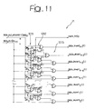
module 11, which is designed to generate, in addition to the signal data_invert also the signal marc_MSb, which, transferred to thecomparison block 14, is used for encoding the bit designed to convey the information INV regarding the possible recourse to the traditional bus-inverter technique, should the comparison step 106' of Figure 2 have detected a difference (flags set in thesteps 114 and 166). - The diagrams of Figures 11, 12 and 13 reproduce, with a formalism altogether equivalent to the one adopted previously in Figures 5, 8 and 9, the structure of the
module 11, as well as of thecomparison module 14 and again of the correspondingdecoder 20 in the case where the solution described in the flowchart of Figure 2 is used. There will be noted, in the diagram of Figure 13, the presence of an additional block, designated by 2014' and designed specifically to decode the signal INV (inv_decoder) in order to see again whether this assumes thevalue 0, the value 0.5 or thevalue 1. The implementation of such a block is evident for a person skilled in the sector. - It will moreover be appreciated that the solution described, illustrated as applied, starting from the most significant bit (MSB) of the signal D(t) and of the signal B(t-1), may be applied starting also from the least significant bit (LSB), namely starting either from the most significant bit or from the least significant bit and then proceed towards the inner bits the datum. The same technique may be also applied starting from any other bit, for example the central one, moving towards the left or towards the right, or again in both directions.
- Basically, the solution described above corresponds to the identification of a subset of bits identified by a marker bit or marker, with the possibility of applying to the subset thus identified any technique for reducing the switching activity, with the added possibility, for the decoder, of identifying the marker bit, and hence the set of bits subjected to encoding precisely because the marker bit is the first bit in the orderly sequence of comparison between D(t) and B(t-1) to have been subjected to said treatment.
- In particular, the solution described herein can be used in a co-ordinated way with a further improvement of the bus-inverter technique such as to redefine the output in the case where the switching activity of the encoded datum is equal to the switching activity of the non-encoded datum.
- The above is achieved by detecting whether the switching activity achieved by sending the encoded datum is equal to the switching activity achieved with the non-encoded datum, by sending in this case the non-encoded datum and setting the signal INV equal to 0.
- In fact, if the switching activity coincides in the two cases, the global switching activity is in any case reduced if the value of the bit INV is left unaltered, i.e., if INV = 0, and the non-encoded datum is sent, maintaining INV always at 0, whereas if INV is equal to 1, then the encoded datum is sent, maintaining INV always at 1.
- In other words, instead of assigning to INV a value equal to 0, which may require INV to pass from 1 to 0 if its preceding value was 1, INV is left with the same value that it already had, when the datum was transmitted; consequently, since, as has already been said, the same value of SA is obtained.
- Basically, the solution described may be expressed in the following terms:


- Of course, without prejudice to the principle of the invention, the details of implementation and the embodiments may be amply varied with respect to what is described and illustrated herein, without thereby departing from the scope of the present invention, as defined in the attached claims.
- It will be appreciated that the solutions described herein as being implementable at the level of specific hardware circuitry, are suitable also for implementation at a software level by means of processing circuits of a general-purpose type appropriately programmed with a computer product which, when run on the said hardware of a general-purpose type, determines the implementation of the solution according to the invention.
Claims (39)
- A process for transmitting at given instants (..., t-1, t, ...) digital signals (D) on a bus (P), said digital signals being transmitted on the bus (P) selectively in a non-encoded format (D(t)) and in an encoded format (NOT(D(t))), the decision whether to transmit said signals on the bus in non-encoded format or in encoded format being taken according to the operation of comparing the signal (D(t)) to be transmitted on the bus (P) for an instant (t) of said given instants with the signal (B(t-1)) used for transmission on the bus (P) for the preceding instant (t-1) among said given instants so as to minimize the switching activity (SA) on the bus (P), the said procedure being characterized in that:- said operation of comparing is carried out bit by bit in orderly sequence so as to identify, in the context of said signal (D(t)) to be transmitted on the bus (P) at an instant (t) of said given instants and of said signal (B(t-1)) used for transmission on the bus (P) for the preceding instant (t-1) among said given instants, a first set of bits that are not changed and a second set of bits that are changed; and- said decision whether to transmit said signals on the bus in non-encoded format (D(t)) and in encoded format (NOT(D(t))) is taken limitedly to the bits of said second set of bits.
- The process according to Claim 1, characterized in that it comprises the operation of identifying, in the context of said orderly sequence, at least one marker bit that separates the bits of said first set from the bits of said second set.
- The process according to Claim 1 or Claim 2, characterized in that said operation of comparison bit by bit is carried out starting from the bit with the least probability of change.
- The process according to any one of the preceding claims, characterized in that said operation of comparison bit by bit is carried out starting from the most significant bit (MSB).
- The process according to any one of the preceding claims, characterized in that said operation of comparison bit by bit is carried out starting from the least significant bit (LSB).
- The process according to any one of Claims 1 to 5, characterized in that said operation of comparison bit by bit is carried out starting from a given bit, exploring the other bits subjected to comparison moving in a given direction.
- The process according to any one of Claims 1 to 5, characterized in that said operation of comparison bit by bit is carried out starting from at least one given bit, exploring the other bits subjected to comparison moving in opposite directions.
- The process according to any one of the preceding claims, characterized in that it comprises the operation of transmitting, in non-encoded format, the first bit (Dn-1(t)) of said signal (D(t)) to be transmitted on the bus.
- The process according to any one of the preceding Claims 1 to 7, characterized in that it comprises the operation of encoding integrally, in view of transmission on the bus (P), said signal (D(t)) to be transmitted on the bus (P) if said comparison operation reveals that the first bit (Dn-1(t)) considered in said orderly sequence is changed.
- The process according to Claim 1, characterized in that it comprises the operation of transmitting on the bus (P) the bits of said first set always in non-encoded format (D(t)).
- The process according to any one of the preceding claims, characterized in that said encoded format (NOT(D(t))) is obtained subjecting to logic inversion the bits of the signal in non-encoded format (D(t)).
- The process according to any one of Claims 1 to 11, characterized in that it comprises the operation of associating to said digital signals (D(t)) an additional signal (INV) that is able to assume, at said given instants (..., t-1, t, ...), different logic values according to whether the digital signal to which it is associated is transmitted in said non-encoded format (D(t)) and, at least in part, in said encoded format (NOT(D(t))), respectively, so that said additional signal is able to modify its logic value between successive instants of said given instants (..., t-1, t, ...);- verifying, for said digital signals (D(t)), recurrence of the condition in which transmission on said bus (P) in said non-encoded format (D(t)) and in said encoded format (NOT (D(t))) are able to give rise to an identical switching activity (SA) on the bus; and- deciding whether the signal (D(t)) to be transmitted on the bus (P) at a given instant (t) is to be transmitted in said non-encoded format (D(t)) or in said at least partially encoded format (NOT(D(t))) so as to cause the additional signal (INV) associated to said signal (D(t)) to be transmitted on the bus (P) at a given instant (t) to keep its logic value with respect to the logic value assumed by the additional signal for transmission on the bus (P) for the preceding instant among said given instants.
- The process according to any one of the preceding claims, characterized in that said switching activity (SA) on the bus is determined as distance between said signal (D(t)) to be transmitted on the bus (P) at an instant (t) among said given instants and the signal (B(t-1)) used for transmission on the bus (P) for the preceding instant (t) among said given instants.
- The process according to Claim 13, characterized in that said distance is determined as Hamming distance.
- An encoder for transmitting at given instants (..., t-1, t, ...) on a bus (P) digital signals selectively (15) in a non-encoded format (D(t)) and an encoded format (NOT(D)t))), the encoder comprising:- at least one comparison module (11, 12, 13) for comparing the signal (D(t)-data_in) to be transmitted on the bus (P) for an instant (t) of said given instants with the signal (B(t-1)-data_out_encoder) used for transmission on the bus (P) for the preceding instant (t-1) among said given instants, and emitting at least one corresponding decision signal (inv_out_comp); and- at least one transmission-driving module (14, 15) for driving the transmission of said signals on the bus in non-encoded format and in encoded format according to said decision signal (inv_out_comp) so as to minimize the switching activity (SA) on the bus,characterized in that:- said at least one comparison module comprises, a logic network (1011, 1012, 1013, 12, 12a, 13, 13a) that is able to compare bit by bit, in orderly sequence, said signal (D(t)) to be transmitted on the bus (P) at an instant (t) of said given instants and said signal (B(t-1)) used for transmission on the bus (P) for the preceding instant (t-1) among said given instants, so as to identify a first set of bits that are not changed and a second set of bits that are changed; and- said at least one transmission-driving module (14, 15) is configured for driving the transmission of said signals on the bus in non-encoded format (D(t)) and in encoded format (NOT(D(t))) limitedly to the bits of said second set of bits.
- The encoder according to Claim 15, characterized in that said logic network (1011, 1012, 1013, 12, 12a, 13, 13a) performs said operation of comparison bit by bit, starting from the bit with least probability of change.
- The encoder according to Claim 15 or Claim 16, characterized in that said logic network (1011, 1012, 1013, 12, 12a, 13, 13a) performs said operation of comparison bit by bit, starting from the most significant bit (MSB) .
- The encoder according to any one of the preceding Claims 15 to 17, characterized in that said logic network (1011, 1012, 1013, 12, 12a, 13, 13a) performs said operation of comparison bit by bit, starting from the least significant bit (LSB).
- The encoder according to any one of Claims 15 to 18, characterized in that said logic network (1011, 1012, 1013, 12, 12a, 13, 13a) performs said operation of comparison bit by bit starting from a given bit, exploring the other bits subjected to comparison, moving in a given direction.
- The encoder according to any one of Claims 15 to 19, characterized in that said logic network (1011, 1012, 1013, 12, 12a, 13, 13a) performs said operation of comparison bit by bit starting from at least one given bit, exploring the other bits subjected to comparison, moving in opposite directions.
- The encoder according to any one of the preceding claims 15 to 20, characterized in that said at least one transmission-driving module (14, 15) is configured for driving the transmission of the first bit (Dn-1(t)) of said signal (D(t)) to be transmitted on the bus in non-encoded format.
- The encoder according to any one of the preceding Claims 15 to 20, characterized in that said at least one transmission-driving module (14, 15) is configured for driving the transmission of said signal (D(t)) to be transmitted on the bus (P) in integrally encoded format, if said logic network (1011, 1012, 1013, 12, 12a, 13, 13a) indicates that the first bit (Dn-1(t)) considered in said orderly sequence is changed.
- The encoder according to Claim 15, characterized in that said at least one transmission-driving module (14, 15) is configured for transmitting on the bus (P) the bits of said first set always in non-encoded format (D(t)).
- The encoder according to any one of the preceding Claims 15 to 23, characterized in that it comprises an inverter circuit (11, 1011, 1012, 1013) for generating said encoded format (NOT(D(t))), subjecting to logic inversion the bits of the signal in non-encoded format (D(t)).
- The encoder according to any one of Claims 15 to 24, characterized in that it comprises:- a module (14) for associating to said digital signals (D(t)) an additional signal (INV) that is able to assume, at said given instants (..., t-1, t, ...), different logic values according to whether the digital signal to which it is associated is transmitted in said non-encoded format (D(t)) or, at least in part, in said encoded format (NOT(D(t))), respectively, so that said additional signal is able to modify its logic value between successive instants of said given instants (..., t-1, t, ...); and- at least one module (12, 13) for verifying, for said digital signals (D(t)), the recurrence of the condition in which the transmission on said bus (P) in said non-encoded format (D(t)) and in said encoded format (NOT (D(t))) are able to give rise to an identical switching activity (SA) on the bus;and in that said at least one transmission-driving module (14, 15) is configured for driving transmission of said signals on the bus in said non-encoded format (D(t)) and in said at least in part encoded format (NOT(D(t))) so as to cause the additional signal (INV) associated to said signal (D(t)) to be transmitted on the bus (P) at a given instant (t) to keep its logic value with respect to the logic value assumed by the additional signal for transmission on the bus (P) for the preceding instant among said given instants.
- The encoder according to any one of the preceding Claims 15 to 25, characterized in that it comprises at least one module (12, 13) for calculating distance for determining said switching activity (SA) on the bus as distance between said signal (D(t)) to be transmitted on the bus (P) at an instant (t) among said given instants and the signal (B(t-1)) used for transmission on the bus (P) for the preceding instant (t) among said given instants.
- The encoder according to Claim 26, characterized in that said at least one module (12, 13) for calculating distance comprises at least one module for calculating the Hamming distance.
- A decoder for receiving digital signals (D) transmitted on a bus (P) with the process according to any one of Claims 1 to 14, characterized in that it comprises:- a decoding logic (2014; 2014') that is able to identify, in the context of each digital signal received, at least one marker bit that separates the bits of said first set from the bits of said second set; and- a logic reconstruction network (2011, 2012, 2013) for reconverting from said encoded format (NOT(D(t))) to said non-encoded format (D(t)) the bits of said second set.
- The decoder according to Claim 28, characterized in that said decoding logic (2014; 2014') is able to identify said at least one marker bit as the bit of said digital signals with least probability of change.
- The decoder according to either Claim 28 or Claim 29, characterized in that said decoding logic (2014; 2014') is able to identify said at least one marker bit as the most significant bit (MSB) of said digital signals (D(t)).
- The decoder according to any one of Claims 28 to 30, characterized in that said decoding logic (2014; 2014') is that it is able to identify said at least one marker bit as the least significant bit (LSB) of said digital signals (D(t)).
- The decoder according to any one of Claims 28 to 31, characterized in that said decoding logic (2014; 2014') is able to identify said at least one marker bit as starting bit for exploring said digital data (D(t)), carried out moving in a given direction.
- The decoder according to any one of Claims 28 to 32, characterized in that said decoding logic (2014; 2014') is able to identify said at least one marker bit as starting bit for exploring said digital data (D(t)), carried out moving in opposite directions.
- The decoder according to any one of the preceding Claims 28 to 33, characterized in that the decoder is configured for assuming as transmitted in non-encoded format the first bit (Dn-1(t)) of said digital signals (D(t) .
- The decoder according to any one of the preceding Claims 28 to 34, characterized in that the always more transmitted in said non-encoded format (D(t)).
- The decoder according to any one of the preceding Claims 28 to 35, characterized in that said logic reconstruction network (2011, 2012, 2013) reconverts said digital signals from said encoded format (NOT(D(t))) to said non-encoded format (D(t)) by means of logic inversion of the bits subjected to encoding.
- A computer program product directly loadable into the memory of a computer and comprising software code portions for implementing the process according to any one of Claims 1 to 14 when said computer product is run on a computer.
- A computer program product directly loadable into the memory of a computer and comprising software code portions for implementing the encoder according to any one of Claims 15 to 27 when the computer product is run on a computer.
- A computer program product directly loadable into the memory of a computer and comprising software code portions for implementing the decoder, according to any one of Claims 28 to 36 when the computer product is run on a computer.
Priority Applications (4)
| Application Number | Priority Date | Filing Date | Title |
|---|---|---|---|
| EP02425575A EP1403774B1 (en) | 2002-09-25 | 2002-09-25 | Process and devices for transmitting digital signals over buses and computer program product therefor |
| DE60221396T DE60221396D1 (en) | 2002-09-25 | 2002-09-25 | Method and apparatus for transmitting digital signal over a computer bus and computer program product therefor |
| US10/670,993 US7372916B2 (en) | 2002-09-25 | 2003-09-25 | Process and devices for transmitting digital signals over buses and computer program product therefore |
| US12/060,809 US7991081B2 (en) | 2002-09-25 | 2008-04-01 | Process and devices for transmitting digital signals over buses and computer program product therefore |
Applications Claiming Priority (1)
| Application Number | Priority Date | Filing Date | Title |
|---|---|---|---|
| EP02425575A EP1403774B1 (en) | 2002-09-25 | 2002-09-25 | Process and devices for transmitting digital signals over buses and computer program product therefor |
Publications (2)
| Publication Number | Publication Date |
|---|---|
| EP1403774A1 true EP1403774A1 (en) | 2004-03-31 |
| EP1403774B1 EP1403774B1 (en) | 2007-07-25 |
Family
ID=31970518
Family Applications (1)
| Application Number | Title | Priority Date | Filing Date |
|---|---|---|---|
| EP02425575A Expired - Fee Related EP1403774B1 (en) | 2002-09-25 | 2002-09-25 | Process and devices for transmitting digital signals over buses and computer program product therefor |
Country Status (3)
| Country | Link |
|---|---|
| US (2) | US7372916B2 (en) |
| EP (1) | EP1403774B1 (en) |
| DE (1) | DE60221396D1 (en) |
Cited By (1)
| Publication number | Priority date | Publication date | Assignee | Title |
|---|---|---|---|---|
| US6946867B2 (en) | 2002-08-21 | 2005-09-20 | Nec Corporation | Data output circuit and data output method |
Families Citing this family (6)
| Publication number | Priority date | Publication date | Assignee | Title |
|---|---|---|---|---|
| DE102005055428B4 (en) * | 2005-11-21 | 2008-01-31 | Siemens Ag | Bus module for connection to a bus system and use of such a bus module in an AS-i bus system |
| KR100960541B1 (en) * | 2005-11-22 | 2010-06-03 | 인텔 코포레이션 | Signal transition feature based coding for serial link |
| US7501963B1 (en) * | 2007-10-17 | 2009-03-10 | Micron Technology, Inc. | Balanced data bus inversion |
| FR2928757B1 (en) * | 2008-03-14 | 2014-06-20 | Centre Nat Rech Scient | METHOD AND DEVICE FOR ENCODING, ELECTRONIC SYSTEM AND RECORDING MEDIUM THEREOF |
| US8448054B2 (en) * | 2009-04-09 | 2013-05-21 | Eric Morgan Dowling | Signal mapper for reducing error coefficient |
| US10126979B2 (en) * | 2016-10-04 | 2018-11-13 | Qualcomm Incorporated | Bus encoding using metadata |
Citations (2)
| Publication number | Priority date | Publication date | Assignee | Title |
|---|---|---|---|---|
| JPH0969075A (en) * | 1995-08-31 | 1997-03-11 | Nippon Telegr & Teleph Corp <Ntt> | Bus circuit |
| WO2002039290A2 (en) * | 2000-11-07 | 2002-05-16 | Intel Corporation | Method and apparatus for reducing simultaneous switching output noise using dynamic bus inversion |
Family Cites Families (19)
| Publication number | Priority date | Publication date | Assignee | Title |
|---|---|---|---|---|
| US3909721A (en) * | 1972-01-31 | 1975-09-30 | Signatron | Signal processing system |
| US4007421A (en) * | 1975-08-25 | 1977-02-08 | Bell Telephone Laboratories, Incorporated | Circuit for encoding an asynchronous binary signal into a synchronous coded signal |
| US4020463A (en) * | 1976-02-27 | 1977-04-26 | Recognition Equipment Incorporated | Apparatus and a method for storage and retrieval of image patterns |
| US4553129A (en) * | 1983-08-05 | 1985-11-12 | Gte Communication Systems Corporation | Data transmission by subrate grouping |
| US5084891A (en) * | 1989-09-08 | 1992-01-28 | Bell Communications Research, Inc. | Technique for jointly performing bit synchronization and error detection in a TDM/TDMA system |
| US5065107A (en) * | 1990-04-19 | 1991-11-12 | University Of Saskatchewan | Phase-locked loop bandwidth switching demodulator for suppressed carrier signals |
| US5280533A (en) * | 1991-06-14 | 1994-01-18 | International Business Machines Corporation | Coding method for skewed transition correction in parallel asynchronous communication systems |
| CA2169514C (en) * | 1995-03-02 | 1999-02-23 | Peter Douglas Bain | Synchronization and error detection in a tdm/tdma system |
| US5719632A (en) * | 1996-01-25 | 1998-02-17 | Ibm Corporation | Motion video compression system with buffer empty/fill look-ahead bit allocation |
| JP2853672B2 (en) * | 1996-09-11 | 1999-02-03 | 日本電気株式会社 | Arithmetic processing unit |
| US6243779B1 (en) * | 1996-11-21 | 2001-06-05 | Integrated Device Technology, Inc. | Noise reduction system and method for reducing switching noise in an interface to a large width bus |
| US5881260A (en) * | 1998-02-09 | 1999-03-09 | Hewlett-Packard Company | Method and apparatus for sequencing and decoding variable length instructions with an instruction boundary marker within each instruction |
| US6269454B1 (en) * | 1998-11-06 | 2001-07-31 | Advanced Micro Devices, Inc. | Maintaining object information concurrent with data optimization for debugging |
| US6606728B1 (en) * | 1999-06-23 | 2003-08-12 | Agere Systems Inc. | Rate (M/N) code encoder, detector, and decoder for control data |
| US6504493B1 (en) * | 2000-10-31 | 2003-01-07 | Marvell International, Ltd. | Method and apparatus for encoding/decoding data |
| US6738945B2 (en) * | 2001-03-14 | 2004-05-18 | Silicon Integrated System Corp. | Signal transmission device and method for avoiding transmission error |
| US6539051B1 (en) * | 2002-03-11 | 2003-03-25 | Cypress Semiconductor Corporation | Parallel framer and transport protocol with distributed framing and continuous data |
| US6667701B1 (en) * | 2002-07-16 | 2003-12-23 | Motorola, Inc. | Variable length decoder |
| EP1403775B1 (en) * | 2002-09-25 | 2006-03-08 | STMicroelectronics S.r.l. | Process and devices for transmiting digital signals over buses and computer program product therefor |
-
2002
- 2002-09-25 DE DE60221396T patent/DE60221396D1/en not_active Expired - Lifetime
- 2002-09-25 EP EP02425575A patent/EP1403774B1/en not_active Expired - Fee Related
-
2003
- 2003-09-25 US US10/670,993 patent/US7372916B2/en active Active
-
2008
- 2008-04-01 US US12/060,809 patent/US7991081B2/en not_active Expired - Lifetime
Patent Citations (2)
| Publication number | Priority date | Publication date | Assignee | Title |
|---|---|---|---|---|
| JPH0969075A (en) * | 1995-08-31 | 1997-03-11 | Nippon Telegr & Teleph Corp <Ntt> | Bus circuit |
| WO2002039290A2 (en) * | 2000-11-07 | 2002-05-16 | Intel Corporation | Method and apparatus for reducing simultaneous switching output noise using dynamic bus inversion |
Non-Patent Citations (1)
| Title |
|---|
| PATENT ABSTRACTS OF JAPAN vol. 1997, no. 07 31 July 1997 (1997-07-31) * |
Cited By (1)
| Publication number | Priority date | Publication date | Assignee | Title |
|---|---|---|---|---|
| US6946867B2 (en) | 2002-08-21 | 2005-09-20 | Nec Corporation | Data output circuit and data output method |
Also Published As
| Publication number | Publication date |
|---|---|
| US20080211701A1 (en) | 2008-09-04 |
| US7372916B2 (en) | 2008-05-13 |
| US20040153927A1 (en) | 2004-08-05 |
| US7991081B2 (en) | 2011-08-02 |
| DE60221396D1 (en) | 2007-09-06 |
| EP1403774B1 (en) | 2007-07-25 |
Similar Documents
| Publication | Publication Date | Title |
|---|---|---|
| US7991081B2 (en) | Process and devices for transmitting digital signals over buses and computer program product therefore | |
| US9172567B2 (en) | Methods and apparatus to reduce signaling power | |
| EP0883950B1 (en) | Transition-controlled digital encoding and signal transmission system | |
| JPH0514420A (en) | Serial signal transmitter | |
| US4218770A (en) | Delay modulation data transmission system | |
| JPH08223048A (en) | Data conversion system | |
| TW201640359A (en) | N-base numbers to physical wire states symbols translation method | |
| JP2001243049A (en) | Device and method for bus encoding/decoding | |
| EP1403775B1 (en) | Process and devices for transmiting digital signals over buses and computer program product therefor | |
| US10880135B2 (en) | Semiconductor device and communication | |
| US20060098731A1 (en) | Digital video data transmission system and method | |
| JP5506232B2 (en) | Multilevel encoding method, decoding method thereof, and multilevel signal transmission apparatus | |
| CN110620635A (en) | Decoding method, apparatus and readable storage medium | |
| JP4000564B2 (en) | Encoding apparatus and method thereof | |
| US11139830B2 (en) | Bit inversion for data transmission | |
| JP2006528449A (en) | Low voltage amplitude signal encoding method and apparatus | |
| WO2001091306A1 (en) | Encoder for transmitting digital image | |
| CN115833845B (en) | Position output device and position output method | |
| KR20100064442A (en) | Encoding/decoding method and device using the same | |
| US20050238125A1 (en) | Method of interfacing a high speed signal | |
| RU2150785C1 (en) | Adaptive system for transmission and reception of digital information | |
| KR101311617B1 (en) | Method and apparatus of address bus coding/decoding for low-power very large scale integration system | |
| KR100574359B1 (en) | Serial data transmitter - receiver and method thereof | |
| JPS5964969A (en) | Coded signal decoding device | |
| US8526294B2 (en) | Data exchange device using orthogonal vectors |
Legal Events
| Date | Code | Title | Description |
|---|---|---|---|
| PUAI | Public reference made under article 153(3) epc to a published international application that has entered the european phase |
Free format text: ORIGINAL CODE: 0009012 |
|
| AK | Designated contracting states |
Kind code of ref document: A1 Designated state(s): AT BE BG CH CY CZ DE DK EE ES FI FR GB GR IE IT LI LU MC NL PT SE SK TR |
|
| AX | Request for extension of the european patent |
Extension state: AL LT LV MK RO SI |
|
| 17P | Request for examination filed |
Effective date: 20040601 |
|
| AKX | Designation fees paid |
Designated state(s): DE FR GB IT |
|
| GRAP | Despatch of communication of intention to grant a patent |
Free format text: ORIGINAL CODE: EPIDOSNIGR1 |
|
| GRAS | Grant fee paid |
Free format text: ORIGINAL CODE: EPIDOSNIGR3 |
|
| GRAA | (expected) grant |
Free format text: ORIGINAL CODE: 0009210 |
|
| AK | Designated contracting states |
Kind code of ref document: B1 Designated state(s): DE FR GB IT |
|
| REG | Reference to a national code |
Ref country code: GB Ref legal event code: FG4D |
|
| REF | Corresponds to: |
Ref document number: 60221396 Country of ref document: DE Date of ref document: 20070906 Kind code of ref document: P |
|
| ET | Fr: translation filed | ||
| PG25 | Lapsed in a contracting state [announced via postgrant information from national office to epo] |
Ref country code: DE Free format text: LAPSE BECAUSE OF FAILURE TO SUBMIT A TRANSLATION OF THE DESCRIPTION OR TO PAY THE FEE WITHIN THE PRESCRIBED TIME-LIMIT Effective date: 20071026 |
|
| PLBE | No opposition filed within time limit |
Free format text: ORIGINAL CODE: 0009261 |
|
| STAA | Information on the status of an ep patent application or granted ep patent |
Free format text: STATUS: NO OPPOSITION FILED WITHIN TIME LIMIT |
|
| 26N | No opposition filed |
Effective date: 20080428 |
|
| PGFP | Annual fee paid to national office [announced via postgrant information from national office to epo] |
Ref country code: GB Payment date: 20110830 Year of fee payment: 10 |
|
| PGFP | Annual fee paid to national office [announced via postgrant information from national office to epo] |
Ref country code: IT Payment date: 20110824 Year of fee payment: 10 |
|
| PGFP | Annual fee paid to national office [announced via postgrant information from national office to epo] |
Ref country code: FR Payment date: 20111007 Year of fee payment: 10 |
|
| GBPC | Gb: european patent ceased through non-payment of renewal fee |
Effective date: 20120925 |
|
| REG | Reference to a national code |
Ref country code: FR Ref legal event code: ST Effective date: 20130531 |
|
| PG25 | Lapsed in a contracting state [announced via postgrant information from national office to epo] |
Ref country code: GB Free format text: LAPSE BECAUSE OF NON-PAYMENT OF DUE FEES Effective date: 20120925 |
|
| PG25 | Lapsed in a contracting state [announced via postgrant information from national office to epo] |
Ref country code: IT Free format text: LAPSE BECAUSE OF NON-PAYMENT OF DUE FEES Effective date: 20120925 Ref country code: FR Free format text: LAPSE BECAUSE OF NON-PAYMENT OF DUE FEES Effective date: 20121001 |