EP1401032A2 - Appareil électroluminescent - Google Patents
Appareil électroluminescent Download PDFInfo
- Publication number
- EP1401032A2 EP1401032A2 EP03021328A EP03021328A EP1401032A2 EP 1401032 A2 EP1401032 A2 EP 1401032A2 EP 03021328 A EP03021328 A EP 03021328A EP 03021328 A EP03021328 A EP 03021328A EP 1401032 A2 EP1401032 A2 EP 1401032A2
- Authority
- EP
- European Patent Office
- Prior art keywords
- light
- insulating film
- film
- electrode
- formed over
- Prior art date
- Legal status (The legal status is an assumption and is not a legal conclusion. Google has not performed a legal analysis and makes no representation as to the accuracy of the status listed.)
- Withdrawn
Links
Images


Classifications
-
- H—ELECTRICITY
- H10—SEMICONDUCTOR DEVICES; ELECTRIC SOLID-STATE DEVICES NOT OTHERWISE PROVIDED FOR
- H10K—ORGANIC ELECTRIC SOLID-STATE DEVICES
- H10K50/00—Organic light-emitting devices
- H10K50/80—Constructional details
- H10K50/87—Arrangements for heating or cooling
-
- H—ELECTRICITY
- H10—SEMICONDUCTOR DEVICES; ELECTRIC SOLID-STATE DEVICES NOT OTHERWISE PROVIDED FOR
- H10K—ORGANIC ELECTRIC SOLID-STATE DEVICES
- H10K50/00—Organic light-emitting devices
- H10K50/80—Constructional details
- H10K50/84—Passivation; Containers; Encapsulations
- H10K50/842—Containers
- H10K50/8426—Peripheral sealing arrangements, e.g. adhesives, sealants
-
- H—ELECTRICITY
- H10—SEMICONDUCTOR DEVICES; ELECTRIC SOLID-STATE DEVICES NOT OTHERWISE PROVIDED FOR
- H10K—ORGANIC ELECTRIC SOLID-STATE DEVICES
- H10K50/00—Organic light-emitting devices
- H10K50/80—Constructional details
- H10K50/84—Passivation; Containers; Encapsulations
- H10K50/844—Encapsulations
-
- H—ELECTRICITY
- H10—SEMICONDUCTOR DEVICES; ELECTRIC SOLID-STATE DEVICES NOT OTHERWISE PROVIDED FOR
- H10K—ORGANIC ELECTRIC SOLID-STATE DEVICES
- H10K59/00—Integrated devices, or assemblies of multiple devices, comprising at least one organic light-emitting element covered by group H10K50/00
- H10K59/10—OLED displays
- H10K59/12—Active-matrix OLED [AMOLED] displays
Definitions
- the present invention relates to a light-emitting apparatus comprising a light-emitting device, which emits fluorescent light or phosphorescent light upon application of an electric field thereto, including a pair of electrodes and an electroluminescent layer that is sandwiched between the pair of electrodes, and to a method of fabricating the light-emitting apparatus.
- the present invention relates to technique for preventing moisture or oxygen from penetrating into the light-emitting device formed on a substrate by using a film containing fluoroplastics.
- the term light-emitting apparatus includes an image display apparatus, a light-emitting device, or a light source (including a lighting system).
- the following modules are included in the light-emitting apparatus: a module obtained by attaching a connector such as an FPC (flexible printed circuit), a TAB (tape automated bonding) tape, or a TCP (tape carrier package) to a light-emitting device; a module obtained by providing a printed wiring board with a tip of a TAB tape or a TCP; and a module obtained by mounting directly an IC (integrated circuit) to a light-emitting device by the COG (chip on glass) system.
- a connector such as an FPC (flexible printed circuit), a TAB (tape automated bonding) tape, or a TCP (tape carrier package)
- a light-emitting device in which a material characterized by their thinness and lightweight, fast response, and direct current low voltage driving is used as an illuminant, is expected to be applied to next-generation flat panel displays.
- a light-emitting apparatus in which light-emitting devices are arranged in matrix are considered to be superior to the conventional liquid crystal display devices for their wide viewing angle and excellent visibility.
- the luminescent mechanism of light-emitting device is as follows: voltage is applied to a pair of electrodes that sandwich an electroluminescent layer, and electrons injected from a cathode and holes injected from an anode are re-combined at the luminescent center of the electroluminescent layer to form molecular excitons, and then the molecular excitons return to the base state while releasing energy, consequently, luminescence is generated in the electroluminescent layer.
- Known excitation states are singlet excitation and triplet excitation, and it is considered that luminescence can be generated by either excitation states.
- a light-emitting apparatus has a problem in the fabrication process, the problem is different from that of another display apparatuses such as a liquid crystal display apparatus, or the like.
- a light-emitting device is deteriorated by moisture. Specifically, due to moisture, exfoliation between an electroluminescent layer and a electrode, deterioration of a material for forming an electroluminescent layer, generation of non light emitting portion referred to as a dark spot, or shrinkage of a light emitting portion resulting to inferior luminescence are seen in the light-emitting device. Such deterioration of the light-emitting device causes decreasing reliability of a light-emitting device in a long-time-driving.
- Teflon@AF a product by DuPont Corp.
- polymer of Teflon@ is formed by vapor deposition to seal a light-emitting device (for example, Reference 1: Patent Publication No. 2597047).
- the relative permittivity of Teflon@ can be controlled to be from 1.9 to 2.1, there are concerns over ramifications of using Teflon@ such as the thermal stability, metal fluorine reaction, or the like.
- it is an object of the present invention is to solve the problem of heat release and metal material corrosion due to fluorine that are arisen in the case of using a film containing fluoroplastics (Teflon@) as a protective film for a light-emitting device.
- an inorganic film is formed after forming a light-emitting device, and a film containing fluoroplastics is formed thereon with avoiding contact with a metal material for forming the light-emitting device, as the result, a metal material corrosion due to fluorine in the film containing fluoroplastics can be prevented.
- an inorganic insulating film formed between a metal film of a light-emitting device (a second electrode) and a film containing fluoroplastics has a function of preventing fluorine in the film containing fluoroplastics from reacting to the metal material (barrier property), in addition, the inorganic insulating film is formed of a material having high heat conductivity for releasing heat generated in a light-emitting device.
- an inorganic material such as silicon nitride, silicon oxynitride (SiNxOy), silicon oxide, aluminum nitride (A1N), aluminum oxynitride (AlNxOy) DLC (diamond like carbon) film, carbon nitride (CxNy) film, or the like is useful for the inorganic insulating film.
- a concrete constitution according to the present invention is: a light-emitting apparatus having a light-emitting device including a first electrode, an electroluminescent film formed on the first electrode, and a second electrode formed on the electroluminescent film, comprising:
- a film containing fluoroplastics is formed on the inorganic insulating film that is formed to cover the metal material for the light-emitting device (the second electrode) for preventing deterioration of the light-emitting device due to moisture or gas such as oxygen or the like.
- a film containing fluoroplastics according to the present invention is formed by sputtering using the target materials such as polytetrafluoroethylene, tetrafluoroethylene-hexafluoropropylene copolymer, polychlorotrifluoroethylene, tetrafluoroethylene-ethylene copolymer, polyvinyl fluoride, polyvinylidene fluoride, or the like.
- target materials such as polytetrafluoroethylene, tetrafluoroethylene-hexafluoropropylene copolymer, polychlorotrifluoroethylene, tetrafluoroethylene-ethylene copolymer, polyvinyl fluoride, polyvinylidene fluoride, or the like.
- Another constitution according to the present invention is that an organic insulating film is formed using an organic insulating material on an inorganic insulating film, and its surface is flattened, and then, a film containing fluoroplastics is formed.
- an organic resin film is formed on an inorganic insulating film (a first insulating film), and another inorganic insulating film (a second insulating film) is formed thereon, and then, a film containing fluoroplastics is formed thereon.
- the organic insulating film is formed any one of acrylic, polyamide, or polyimide.
- a light-emitting apparatus having a light-emitting device including a first electrode connecting electrically to a TFT formed on a substrate via an insulating film, an electroluminescent film formed on the first electrode, and a second electrode formed on the electroluminescent film, comprising:
- a film containing fluoroplastics that has a property of heat release for a light-emitting device and is capable of preventing a metal material corrosion due to fluorine can be formed as a protective film of the light emitting device.
- a film containing fluoroplastics formed by sputtering can be formed on the surface of another finished product (the surface that is exposed to the air or man's hands).
- Embodiment Mode 1 the case in which an inorganic insulating film that has a heat release property and a barrier property against fluorine, and a film containing fluoroplastics that has a function for preventing moisture or gas such as oxygen or the like from penetrating are stacked on a second electrode after forming the light-emitting device will be described with reference to Fig. 1.
- a bottom emitting type light-emitting apparatus in which light generated in a light-emitting device emits in the direction of the substrate on which TFT is formed and a top emitting type light-emitting apparatus in which light generated in a light-emitting device emits in the opposite direction of the substrate.
- a top emitting type light-emitting apparatus in which light generated in a light-emitting device emits in the opposite direction of the substrate.
- Fig. 1 is a cross-sectional view showing a part of a pixel portion.
- reference numeral 101 is a first substrate; 102a, 102b, 102c are insulating layers; 103 is a TFT (including a gate electrode 104, a channel formation region 105, and an impurity region 106); 107 is a wiring; 108 is a first electrode; 109 is an insulating film; 110 is an electroluminescent layer; 111 is a second electrode; 112 is an inorganic insulating film; and 113 is film containing fluoroplastics.
- the insulating layer 102a that serves as a base insulating film (here, a bottom layer is a nitride insulating film, and an upper layer is an oxide insulating film) is formed on the first substrate 101, and the insulating layer 102b is formed between the gate electrode 104 and an active layer.
- the insulating layer 102c that serves as an interlayer insulating film formed of an organic material or an inorganic material is formed on the gate electrode 104.
- the TFT 103 (here, p-channel TFT is used) formed on the first substrate 101 in contact with the insulating layer 102a is an element for controlling the current passing through the electroluminescent layer 110.
- Reference numeral 106 is an impurity region (a drain region or a source region).
- Reference numeral 107 is a wiring (also referred to as a drain electrode or a source electrode) for connecting a first electrode 108 to the impurity region 106.
- a current supply line, a source wiring, or the like is formed simultaneously in similar process.
- TFT n-channel TFT or a p-channel TFT.
- the first electrode 108 serves as an anode. Therefore as a material for forming the first electrode, it is preferable to use a large work function material (not less than 4.0eV).
- a large work function material not less than 4.0eV.
- TiN, TiSi x N y , WSi x , WN x , WSi x , N y , NbN, indium-tin-oxides (ITO), indium-zinc-oxides (IZO), an alloy of indium and one type or plural types of metallic oxides (for example, indium aluminum oxides, indium tungsten oxides, indium germanium oxides, indium titanium oxides, indium tantalum oxides, or the like), or ITO-SiO 2 (for example, In 2 O 3 : SnO 2 : SiO 2 85: 10: 5 (wt%), or the like), in addition, an element selected from Ti, Ni, W, Mo, Cr, Pt, Zn, S
- a titanium nitride film is used as the first electrode 108.
- An insulator 109 (also referred to as a bank) is formed that covers an edge portion of the first electrode 108 (and wiring 107).
- a material for the insulator 109 an inorganic material (silicon oxide, silicon nitride, silicon oxynitride, or the like), a photosensitive organic material, a nonphotosensitive organic material (polyimide, acrylic, polyamide, polyimideamide, resist, or benzocyclobutene), or a lamination layer of these materials can be appropriately used.
- a photosensitive organic resin covered by a silicon nitride film is used for the insulator 109 here.
- an only upper edge portion of the insulator is formed to have a curved surface having a radius of curvature.
- Either a negative type that is a soluble material in etchant according to photosensitive light or a positive type that is dissoluble in etchant according to light can be used as an insulator.
- the electroluminescent layer 110 is formed by vapor deposition or coating.
- the substrate is heated in vacuum (from 100 to 250°C) for degasification just before forming the electroluminescent layer 110 in order to improve reliability.
- white light emission can be obtained by forming the electroluminescent layer 110 having the configuration: an Alq 3 film, an Alq 3 film partially doped with Nile red which is a red luminescent pigment, an Alq 3 film, a p-EtTAZ film, and a TPD (aromatic diamine) film, sequentially.
- the spin-coated film is preferable to be baked by vacuum heating.
- an aqueous solution of poly(ethylene dioxythiophene)/poly(styrene sulfonic acid) (PEDOT/PSS) is coated on the entire surface and baked to form a film that serves as a hole injection layer.
- PVK polyvinyl carbazole
- a luminescence center pigment such as 1, 1, 4, 4-tetraphenyl-1, 3-butadiene (TPB), 4-dicyanomethylene-2-methyl-6-(p-dimethylamino-styryl)-4H-pyran (DCM1), Nile red, or coumarin 6
- TPB 1, 1, 4, 4-tetraphenyl-1, 3-butadiene
- DCM1 4-dicyanomethylene-2-methyl-6-(p-dimethylamino-styryl)-4H-pyran
- Nile red or coumarin 6
- the electroluminescent layer 110 may be formed to have a single layer structure.
- a 1, 3, 4-oxadiazole derivative (PBD) having an electron transporting property is dispersed in polyvinyl carbazole (PVK) having hole transporting property.
- PVK polyvinyl carbazole
- Another method to obtain white light emission is to disperse 30 wt% PBD as an electron transporting agent and disperse four kinds of pigments (TPB, coumarin 6, DCM1, and Nile red) in appropriate amounts.
- red, green, and blue-light-emitting devices can be obtained by selecting appropriately a material for forming the electroluminescent layer 110.
- a second electrode 111 serves as a cathode for a light-emitting device in Embodiment Mode 1, it is preferable to use a small work function material (not more than 3.5eV) for forming the second electrode 111.
- a small work function material not more than 3.5eV
- the top emitting type light-emitting apparatus described in Embodiment Mode 1 requires the second electrode 111 to be transparent to light. Consequently, the second electrode 111 is formed using an aluminum film having a thickness from 1nm to 10nm, or an aluminum film containing slight amount of Li. In this case, a layer that is transparent to light can be formed of CaF 2 , MgF 2 , or BaF 2 (thickness from 1 to 5nm) as a cathode buffer layer.
- the second electrode 111 In order to decrease resistance of the second electrode 111, it can be formed to be a lamination structure of a thin metal film and a transparent conductive film (Indium-tin-oxide (ITO), indium oxide-zinc oxide (In 2 O 3 -ZnO), zinc oxide (ZnO), or the like). Otherwise, a support electrode can be formed on a part of the second electrode 111 that is not overlapped with a light-emitting region.
- ITO Indium-tin-oxide
- ITO indium oxide-zinc oxide
- ZnO zinc oxide
- the inorganic insulating film 112 is formed to have a thickness from 0.1 to 1 ⁇ m.
- a film containing fluoroplastics 113 can be formed by sputtering or vapor deposition.
- the film containing fluoroplastics 113 protects the second electrode 111 and prevents moisture or gas such as oxygen or the like that cause deterioration of a light-emitting device from penetrating into a light-emitting device 114.
- the target of polytetrafluoroethylene, tetrafluoroethylene-hexafluoropropylene copolymer, polychlorotrifluoroethylene, tetrafluoroethylene-ethylene copolymer, polyvinyl fluoride, polyvinylidene fluoride, or the like is used.
- the film containing fluoroplastics 113 is formed by sputtering.
- the deposition is carried out under the conditions, that is, Ar gas used as process gas is 30sccm (the 5sccm O 2 gas can be used in addition to the Ar gas); sputtering pressure used is 0.4Pa; electric power, 400W; and the substrate temperature, 300°C.
- the film containing fluoroplastics 113 is formed to have a thickness from 0.1 to 5 ⁇ m.
- the film containing fluoroplastics 113 can be formed using a target of fluoroplastics by high-frequency sputtering with applying from 0.15 to 6.2 W per square centimeter high frequency electric power.
- a film containing fluoroplastics 113 that has a property of heat release for a light-emitting device and is capable of preventing a metal material corrosion due to fluorine can be formed as a protective film of the light emitting device.
- Fig. 2 is illustrated the structure: a second electrode 111, an inorganic insulating film 112, an organic insulating film 213, and a film containing fluoroplastics 214, are formed sequentially.
- the organic insulating film 213 can be formed by spin-coating or coating.
- an organic material such as acrylic, polyimide, polyamide, polyimideamide, BCB (benzocyclobutene), or the like is also useful. Forming the organic insulating film 213 of an organic material gives the good flatness on the film surface, in addition, parasitic capacitance can be reduced since an organic material has generally low dielectric constant.
- a second electrode an inorganic insulating film 312, an organic insulating film 213, a second insulating film 314, and an insulating film containing fluoroplastics 315 are formed sequentially.
- the first insulating film 312 can be formed using a material that is used for forming inorganic insulating film 112 shown in Fig. 1 or 2 to have a thickness of in the same range.
- the second inorganic insulating film 314 formed on the organic insulating film 213 can be formed in the same way as that of the first inorganic insulating film 312.
- a material for the first insulating film 312 and the second insulating film 314 and thickness thereof are not necessary to be the same.
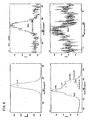
- a film used for the measurement is the film containing fluoroplastics formed to have a thickness of 100nm by using target of polytetrafluoroethylene by sputtering under the conditions, that is, Ar gas used as process gas is 30sccm; sputtering pressure used is 0.4Pa; electric power, 400W; and the substrate temperature, 300°C.
- Fig. 6 is a view showing spectrums of ESCA (photoelectron spectroscopy for chemical analysis). Chemical composition of fluoride, oxygen, carbon, and silicon in the sample is in a ratio of 61: ⁇ 1:38: ⁇ 0.
- Fig. 7 Measured results of a film formed by much the same measuring method in a different deposition condition is illustrated in Fig. 7.
- 30sccm Ar gas and 5sccm O 2 gas are introduced.
- the composition ratio is the same as the condition illustrated in Fig. 6.
- Fig. 8 is a graph showing qualitative analysis results by Fourier transform infrared spectroscopy (FT-IR). It is considered that reference numerals 1, 2, and 3 in Fig. 8 represent peaks derived from CF (1100 to 1000cm -1 ), CF 2 (1250 to 1070cm -1 ), and CF 3 (1360 to 1150cm- 1 ). Since the peak represented by numeral 2 is distinctive, it can be thought that CF 2 is contained at high rates in the film containing fluoroplastics.
- FT-IR Fourier transform infrared spectroscopy
- Fig. 4A is a top surface view of a light-emitting apparatus and Fig. 4B is a cross-sectional view taken along the line of A-A' of Fig. 4A.
- Reference numeral 601 indicated by a dotted line is a drive circuit portion (a source side drive circuit)
- 602 is a pixel portion
- 603 is a drive circuit portion (a gate side drive circuit)
- 604 is a sealing substrate
- 605 is a sealing agent
- 607 surrounded by the sealing agent 605 is a space.
- Reference numeral 608 is a wiring for transmitting signals to be inputted to the source side drive circuit 601 and a gate side drive circuit 603.
- the wiring 608 receives a video signal, a clock signal, a start signal, a reset signal, or the like from the FPC (a flexible printed circuit) 609 that serves as an external input terminal.
- FPC flexible printed circuit
- a PWB a print wiring board
- the light-emitting apparatus in the specification includes not only a body of light-emitting apparatus but also a light-emitting apparatus in the state of being attached with FPC or PWB.
- the source side drive circuit 601 portion that serves as a drive circuit portion and the pixel portion 602 are fabricated on a substrate 610.
- the source side drive circuit 601 is a CMOS circuit that is formed by combining an n-channel TFT 623 and a p-channel TFT 624.
- a TFT for forming a drive circuit may be formed of a known CMOS circuit, PMOS circuit, or NMOS circuit.
- a drive circuit is formed on a substrate that is referred to a driver integrated type is described in this embodiment mode, but not exclusively, the drive circuit may be formed outside.
- the pixel portion 602 comprises a switching TFT 611, a current control TFT 612, and a first electrode 613 that connects electrically to a drain of the current control TFT 612.
- An insulator 614 is formed to cover the edge portion of the first electrode 613.
- the insulator 614 is formed of a positive type photosensitive acrylic resin film.
- the upper end portion or the bottom end portion of the insulator 614 is formed to have a curved surface having curvature.
- a positive type photosensitive acrylic is used as a material for the insulator 614
- Either a negative type that is a soluble material in etchant according to photosensitive light or a positive type that is dissoluble in etchant according to light can be used as an insulator 614.
- An electroluminescent layer 616 and a second electrode 617 are formed respectively on the first electrode 613.
- a material for forming the first electrode 613 it is preferable to use a large work function materials.
- a single layer of a titanium nitride film, a chrome film, a tungsten film, a Zn film, or Pt film, or a lamination of a film containing titanium nitride and aluminum as its main components and the above single layer, or a three-layer lamination of the film containing titanium nitride and aluminum as its main components, a titanium nitride film, and the above single layer are useful for the first electrode 613.
- the first electrode By forming the first electrode to have a lamination structure, resistance as a wiring can be low forming the ohmic contact to the electroluminescent layer 616.
- the first electrode can serve as an anode.
- the electroluminescent layer 616 is formed by vapor deposition using an evaporation mask or ink-jetting.
- the second electrode (cathode) 617 formed on the electroluminescent layer 616 As a material for the second electrode (cathode) 617 formed on the electroluminescent layer 616, a small work function material (Al, Ag, Li, Ca, or alloy of these materials such as MgAg, Mgln, AlLi, CaF 2 , or CaN) is useful.
- the second electrode (cathode) 617 is formed of a lamination of a thin metal film, a transparent conductive film (Indium-tin-oxide (ITO), indium oxide-zinc oxide (In 2 O 3 -ZnO), zinc oxide (ZnO), or the like) in order the second electrode to transmit light.
- ITO Indium-tin-oxide
- ITO indium oxide-zinc oxide
- ZnO zinc oxide
- the second electrode 617 serves as a wiring in common with all of the pixels and connects electrically to the FPC 609 via a connection wiring 608.
- An inorganic insulating film 619 is formed on the second electrode 617.
- a silicon nitride film, a silicon oxide film, a silicon oxynitride film (SiNO film (in a composition ratio of N>O) or SiON film (in a composition ratio of N ⁇ O)) or a thin film containing carbon as its main components (for example, a DLC film, a CN film, or the like) formed by sputtering, CVD, or vapor deposition may be useful for the inorganic insulating film 619.
- a film containing fluoroplastics 620 is formed on the inorganic insulating film 619 by sputtering.
- Fluoroplastics such as polytetrafluoroethylene, tetrafluoroethylene-hexafluoropropylene copolymer, polychlorotrifluoroethylene, tetrafluoroethylene-ethylene copolymer, polyvinyl fluoride, polyvinylidene fluoride, or the like is useful for forming the film containing fluoroplastics 620.
- the light-emitting device 618 is encapsulated in the space 607 enclosed with the substrate 610, the sealing substrate 604, and the sealant 605.
- epoxy resin for forming the sealant 605. Further, preferably, these materials transmit little moisture or gas such as oxygen.
- a plastic substrate of a FRP fiberglass-reinforced plastics
- a PVF polyvinyl fluoride
- a myler a polyester, acrylic, or the like
- a polyester a polyester, acrylic, or the like
- Embodiment Mode can be freely combined with Embodiment Mode 1 or Embodiment Mode 2.
- the light-emitting apparatus using a light-emitting device is a self-luminous type, it has high visibility in a light place and a wide viewing angle compared with a liquid crystal display apparatus. Therefore various electric appliances can be completed by employing the light-emitting apparatus according to the present invention.
- a video camera a digital camera; a goggle type display (head mounted display); a navigation system; an audio reproducing device (car audio, an audio component, etc.); a laptop computer; a game machine; a portable information terminal (a mobile computer, a cellular phone, a portable game machine, an electronic book, etc.); and an image reproducing device (specifically, a device that is equipped with a display device for reproducing data in a recording medium such as a digital versatile disk (DVD)).
- a video camera a digital camera
- a goggle type display head mounted display
- a navigation system an audio reproducing device (car audio, an audio component, etc.); a laptop computer; a game machine; a portable information terminal (a mobile computer, a cellular phone, a portable game machine, an electronic book, etc.); and an image reproducing device (specifically, a device that is equipped with a display device for reproducing data in a recording medium such as a digital versatile disk (DVD)).
- the light-emitting apparatus using a light-emitting device is desirable particularly for a portable information terminal since its screen is often viewed obliquely and is required to have a wide viewing angle.
- Specific examples of the electric appliances are shown in Figs. 5A to 5H.
- Fig. 5A shows a display device, which comprises a casing 2001, a supporting base 2002, a display unit 2003, speaker units 2004, a video input terminal 2005, etc.
- the display device can be completed by using the light-emitting apparatus according to the present invention as the display unit 2003.
- the light-emitting apparatus having a light-emitting device is a self-luminous type and does not need a backlight, so that is can be formed into a thinner display device than that of a liquid crystal display device.
- the term display device includes all of the display device for displaying information such as one for a personal computer, one for receiving TV broadcasting, and one for advertisement.
- Fig. 5B shows a digital still camera, which comprises a main body 2101, a display unit 2102, an image receiving unit 2103, operation keys 2104, an external connection port 2105, a shutter 2106, etc.
- the digital still camera can be completed by using the light-emitting apparatus according to the present invention as the display unit 2102.
- Fig. 5C shows a laptop computer, which comprises a main body 2201, a casing 2202, a display unit 2203, a keyboard 2204, an external connection port 2205, a pointing mouse 2206, etc.
- the laptop computer can be completed by using the light-emitting apparatus according to the present invention as the display unit 2203.
- Fig. 5D shows a mobile computer, which comprises a main body 2301, a display unit 2302; a switch 2303, operation keys 2304, an infrared ray port 2305, etc.
- the mobile computer can be completed by using the light-emitting apparatus according to the present invention as the display unit 2302.
- Fig. 5E shows a portable image reproducing device equipped with a recording medium (a DVD player, to be specific).
- the device comprises a main body 2401, a casing 2402, a display unit A 2403, a display unit B 2404, a recording medium (DVD, or the like) reading unit 2405, operation keys 2406, speaker units 2407, etc.
- the display unit A 2403 mainly displays image information whereas the display unit B 2404 mainly displays text information.
- the portable image-reproducing device can be completed by using the light-emitting apparatus according to the present invention as the display units A 2403 and B 2404.
- the term image reproducing device equipped with a recording medium includes video game machines.
- Fig. 5F shows a goggle type display (head mounted display), which comprises a main body 2501, display units 2502, and arm units 2503.
- the mobile computer can be completed by using the light-emitting apparatus according to the present invention as the display units 2502.
- Fig. 5G shows a video camera, which comprises a main body 2601, a display unit 2602, a casing 2603, an external connection port 2604, a remote control receiving unit 2605, an image receiving unit 2606, a battery 2607, an audio input unit 2608, operation keys 2609, an eye piece 2610, etc.
- the video camera can be completed by using the light-emitting apparatus according to the present invention as the display unit 2602.
- Fig. 5H shows a cellular phone, which comprises a main body 2701, a casing 2702, a display unit 2703, an audio input unit 2704, an audio output unit 2705, operation keys 2706, an external connection port 2707, an antenna 2708, etc.
- the video camera can be completed by using the light-emitting apparatus according to the present invention as the display unit 2703. If the display unit 2703 displays white characters on a black background, power consumption of the cellular phone can be reduced.
- the light-emitting apparatus can be employed also in a front or rear projector in which light bearing outputted image information is magnified by a lens or the like to be projected on a screen.
- the electric appliances given in the above often displays information distributed through electronic communication lines such as Internet and CATV (cable television), especially, animation information with increasing frequency.
- the light-emitting apparatus is suitable for displaying animation information since organic light emitting materials have fast response speed.
- the light-emitting apparatus portions that emit light consume power. Therefore it is desirable to display information such that as small portions as possible emit light. Accordingly, if the light-emitting apparatus is used for a display unit that mainly displays text information such as a portable information terminal, in particular, a cellular phone, and an audio reproducing device, it is desirable to assign light emitting portions to display text information while portions that do not emit light serve as the background.
- a display unit that mainly displays text information such as a portable information terminal, in particular, a cellular phone, and an audio reproducing device
- Embodiment Mode 4 may use any of the structures shown in Embodiment Mode 1 to Embodiment Mode 3.
- the present invention by implementing the present invention, not only deterioration of the light-emitting device due to penetration of moisture or gas such as oxygen thereinto can be prevented, but also corrosion of a metal material for forming the light-emitting device can be prevented.
Applications Claiming Priority (2)
| Application Number | Priority Date | Filing Date | Title |
|---|---|---|---|
| JP2002276382 | 2002-09-20 | ||
| JP2002276382A JP2004119016A (ja) | 2002-09-20 | 2002-09-20 | 発光装置 |
Publications (2)
| Publication Number | Publication Date |
|---|---|
| EP1401032A2 true EP1401032A2 (fr) | 2004-03-24 |
| EP1401032A3 EP1401032A3 (fr) | 2007-06-13 |
Family
ID=31944624
Family Applications (1)
| Application Number | Title | Priority Date | Filing Date |
|---|---|---|---|
| EP03021328A Withdrawn EP1401032A3 (fr) | 2002-09-20 | 2003-09-19 | Appareil électroluminescent |
Country Status (6)
| Country | Link |
|---|---|
| US (1) | US7268487B2 (fr) |
| EP (1) | EP1401032A3 (fr) |
| JP (1) | JP2004119016A (fr) |
| KR (1) | KR20040025834A (fr) |
| CN (1) | CN100576595C (fr) |
| TW (1) | TWI369917B (fr) |
Families Citing this family (20)
| Publication number | Priority date | Publication date | Assignee | Title |
|---|---|---|---|---|
| JP2004119015A (ja) * | 2002-09-20 | 2004-04-15 | Semiconductor Energy Lab Co Ltd | 発光装置およびその作製方法 |
| US20040099926A1 (en) * | 2002-11-22 | 2004-05-27 | Semiconductor Energy Laboratory Co., Ltd. | Semiconductor device, display device, and light-emitting device, and methods of manufacturing the same |
| US7652359B2 (en) * | 2002-12-27 | 2010-01-26 | Semiconductor Energy Laboratory Co., Ltd. | Article having display device |
| JP4785415B2 (ja) * | 2004-05-14 | 2011-10-05 | 株式会社半導体エネルギー研究所 | エレクトロルミネッセンス表示装置の作製方法 |
| ATE476757T1 (de) * | 2004-10-21 | 2010-08-15 | Lg Display Co Ltd | Organische elektrolumineszente vorrichtung und herstellungsverfahren |
| WO2007055299A1 (fr) * | 2005-11-09 | 2007-05-18 | Semiconductor Energy Laboratory Co., Ltd. | Dispositif semi-conducteur et procédé pour le fabriquer |
| EP2031036B1 (fr) * | 2007-08-31 | 2012-06-27 | Semiconductor Energy Laboratory Co., Ltd. | Élément électroluminescent, dispositif électroluminescent, et appareil électronique |
| WO2009110136A1 (fr) * | 2008-03-04 | 2009-09-11 | シャープ株式会社 | Substrat de dispositif d'affichage, son procédé de fabrication, dispositif d'affichage, procédé de formation d'un câblage multicouche et substrat à câblage multicouche |
| TWI388056B (zh) * | 2008-12-05 | 2013-03-01 | Chunghwa Picture Tubes Ltd | 有機電致發光元件 |
| TWI589042B (zh) | 2010-01-20 | 2017-06-21 | 半導體能源研究所股份有限公司 | 發光裝置,撓性發光裝置,電子裝置,照明設備,以及發光裝置和撓性發光裝置的製造方法 |
| US9000442B2 (en) * | 2010-01-20 | 2015-04-07 | Semiconductor Energy Laboratory Co., Ltd. | Light-emitting device, flexible light-emitting device, electronic device, and method for manufacturing light-emitting device and flexible-light emitting device |
| KR101033963B1 (ko) * | 2010-09-24 | 2011-05-11 | 엘지이노텍 주식회사 | 발광 소자 어레이 모듈 및 그의 보호막 형성 방법 |
| KR20120109081A (ko) * | 2011-03-24 | 2012-10-08 | 삼성디스플레이 주식회사 | 유기 발광 표시 장치 |
| CN102856503A (zh) * | 2011-06-28 | 2013-01-02 | 海洋王照明科技股份有限公司 | 一种有机电致发光器件及其制备方法 |
| CN103035663B (zh) * | 2011-10-04 | 2016-08-10 | 乐金显示有限公司 | 显示器件 |
| KR101643012B1 (ko) * | 2011-10-04 | 2016-07-28 | 엘지디스플레이 주식회사 | 표시장치 |
| KR102000709B1 (ko) * | 2012-08-31 | 2019-09-30 | 삼성디스플레이 주식회사 | 디스플레이 패널의 제조방법 |
| JP6154470B2 (ja) * | 2013-08-28 | 2017-06-28 | シャープ株式会社 | エレクトロルミネッセンス装置、及びその製造方法 |
| KR102539668B1 (ko) * | 2016-06-30 | 2023-06-02 | 엘지이노텍 주식회사 | 반도체 소자, 이를 포함하는 표시패널, 표시장치, 통신장치 |
| KR102421576B1 (ko) * | 2017-03-10 | 2022-07-18 | 삼성디스플레이 주식회사 | 유기 발광 표시 장치 및 유기 발광 표시 장치의 제조 방법 |
Citations (2)
| Publication number | Priority date | Publication date | Assignee | Title |
|---|---|---|---|---|
| WO2000065670A1 (fr) * | 1999-04-28 | 2000-11-02 | E.I. Du Pont De Nemours And Company | Dispositif electronique organique souple presentant une meilleure resistance a la degradation due a l'oxygene et a l'humidite |
| US20010055841A1 (en) * | 2000-04-17 | 2001-12-27 | Shunpei Yamazaki | Light emitting device and manufacturing method thereof |
Family Cites Families (54)
| Publication number | Priority date | Publication date | Assignee | Title |
|---|---|---|---|---|
| JPS5435780B2 (fr) * | 1974-07-23 | 1979-11-05 | ||
| US4417174A (en) * | 1980-10-03 | 1983-11-22 | Alps Electric Co., Ltd. | Electroluminescent cell and method of producing the same |
| JPS60115944A (ja) | 1983-11-29 | 1985-06-22 | Asahi Chem Ind Co Ltd | 電子写真用感光体 |
| US4580818A (en) * | 1984-10-25 | 1986-04-08 | Lyng William E | Locker latching assembly |
| JPH0265895U (fr) * | 1988-11-07 | 1990-05-17 | ||
| JPH03153859A (ja) | 1989-11-08 | 1991-07-01 | Sekisui Chem Co Ltd | 表面改質プラスチック |
| US5188876A (en) * | 1990-04-12 | 1993-02-23 | Armstrong World Industries, Inc. | Surface covering with inorganic wear layer |
| JP2597047B2 (ja) | 1990-12-28 | 1997-04-02 | 出光興産株式会社 | 有機エレクトロルミネッセンスデバイス |
| DE69129907T2 (de) * | 1990-11-30 | 1998-12-10 | Idemitsu Kosan Co | Organische elektroluminszente vorrichtung |
| JP2813495B2 (ja) | 1991-07-26 | 1998-10-22 | 出光興産株式会社 | 有機el素子の封止方法 |
| JP2813499B2 (ja) | 1991-09-30 | 1998-10-22 | 出光興産株式会社 | 有機el素子 |
| JPH05101884A (ja) | 1991-10-11 | 1993-04-23 | Idemitsu Kosan Co Ltd | 有機エレクトロルミネツセンス素子の封止方法及びパターン化方法 |
| JPH06306591A (ja) | 1993-04-28 | 1994-11-01 | Sekisui Chem Co Ltd | 撥水性ハードコート皮膜の製造方法 |
| US5834327A (en) * | 1995-03-18 | 1998-11-10 | Semiconductor Energy Laboratory Co., Ltd. | Method for producing display device |
| US6027958A (en) * | 1996-07-11 | 2000-02-22 | Kopin Corporation | Transferred flexible integrated circuit |
| CN1495523A (zh) * | 1996-08-27 | 2004-05-12 | ������������ʽ���� | 转移方法和有源矩阵基板的制造方法 |
| JP3809681B2 (ja) | 1996-08-27 | 2006-08-16 | セイコーエプソン株式会社 | 剥離方法 |
| EP0946993B8 (fr) * | 1996-09-04 | 2007-09-12 | Cambridge Display Technology Limited | Depot d'electrode pour dispositifs electroluminescents organiques |
| US5952778A (en) * | 1997-03-18 | 1999-09-14 | International Business Machines Corporation | Encapsulated organic light emitting device |
| JPH10321374A (ja) * | 1997-05-20 | 1998-12-04 | Tdk Corp | 有機el素子 |
| US6198220B1 (en) * | 1997-07-11 | 2001-03-06 | Emagin Corporation | Sealing structure for organic light emitting devices |
| US6800378B2 (en) * | 1998-02-19 | 2004-10-05 | 3M Innovative Properties Company | Antireflection films for use with displays |
| TW420965B (en) * | 1998-07-14 | 2001-02-01 | Matsushita Electric Ind Co Ltd | Dispersion-type electroluminescence element |
| US6198092B1 (en) * | 1998-08-19 | 2001-03-06 | The Trustees Of Princeton University | Stacked organic photosensitive optoelectronic devices with an electrically parallel configuration |
| US6274887B1 (en) * | 1998-11-02 | 2001-08-14 | Semiconductor Energy Laboratory Co., Ltd. | Semiconductor device and manufacturing method therefor |
| US6652938B1 (en) * | 1998-11-09 | 2003-11-25 | Kaneka Corporation | Media transport belt |
| TW527735B (en) * | 1999-06-04 | 2003-04-11 | Semiconductor Energy Lab | Electro-optical device |
| TW522453B (en) * | 1999-09-17 | 2003-03-01 | Semiconductor Energy Lab | Display device |
| JP3942770B2 (ja) * | 1999-09-22 | 2007-07-11 | 株式会社半導体エネルギー研究所 | El表示装置及び電子装置 |
| JP2001267578A (ja) * | 2000-03-17 | 2001-09-28 | Sony Corp | 薄膜半導体装置及びその製造方法 |
| US6936485B2 (en) * | 2000-03-27 | 2005-08-30 | Semiconductor Energy Laboratory Co., Ltd. | Method of manufacturing a light emitting device |
| US6664732B2 (en) * | 2000-10-26 | 2003-12-16 | Semiconductor Energy Laboratory Co., Ltd. | Light emitting device and manufacturing method thereof |
| TW522577B (en) * | 2000-11-10 | 2003-03-01 | Semiconductor Energy Lab | Light emitting device |
| US6583440B2 (en) * | 2000-11-30 | 2003-06-24 | Seiko Epson Corporation | Soi substrate, element substrate, semiconductor device, electro-optical apparatus, electronic equipment, method of manufacturing the soi substrate, method of manufacturing the element substrate, and method of manufacturing the electro-optical apparatus |
| US6717181B2 (en) * | 2001-02-22 | 2004-04-06 | Semiconductor Energy Laboratory Co., Ltd. | Luminescent device having thin film transistor |
| JP4147008B2 (ja) | 2001-03-05 | 2008-09-10 | 株式会社日立製作所 | 有機el素子に用いるフィルム及び有機el素子 |
| US20020153833A1 (en) * | 2001-04-18 | 2002-10-24 | Alvin Wu | Full-color electroluminescent lamp and manufacturing method for same |
| US7211828B2 (en) * | 2001-06-20 | 2007-05-01 | Semiconductor Energy Laboratory Co., Ltd. | Light emitting device and electronic apparatus |
| JP2003084123A (ja) * | 2001-06-29 | 2003-03-19 | Seiko Epson Corp | カラーフィルタ基板、カラーフィルタ基板の製造方法、液晶表示装置、電気光学装置、電気光学装置の製造方法及び電子機器 |
| TW564471B (en) * | 2001-07-16 | 2003-12-01 | Semiconductor Energy Lab | Semiconductor device and peeling off method and method of manufacturing semiconductor device |
| KR100413450B1 (ko) * | 2001-07-20 | 2003-12-31 | 엘지전자 주식회사 | 표시소자의 보호막 구조 |
| TW490868B (en) * | 2001-08-10 | 2002-06-11 | Ritdisplay Corp | Method for forming a waterproof layer of organic light emitting device |
| TW554398B (en) * | 2001-08-10 | 2003-09-21 | Semiconductor Energy Lab | Method of peeling off and method of manufacturing semiconductor device |
| KR100393229B1 (ko) * | 2001-08-11 | 2003-07-31 | 삼성전자주식회사 | 자기 정렬된 게이트 구조를 포함하는 불휘발성 메모리장치 제조 방법 및 이에 의한 불휘발성 메모리 장치 |
| US20030048074A1 (en) * | 2001-09-12 | 2003-03-13 | Jui-Ming Ni | Method for packaging organic electroluminescent components with polymer passivation layer and structure thereof |
| US7071613B2 (en) * | 2001-10-10 | 2006-07-04 | Lg.Philips Lcd Co., Ltd. | Organic electroluminescent device |
| US6926572B2 (en) * | 2002-01-25 | 2005-08-09 | Electronics And Telecommunications Research Institute | Flat panel display device and method of forming passivation film in the flat panel display device |
| US7164155B2 (en) * | 2002-05-15 | 2007-01-16 | Semiconductor Energy Laboratory Co., Ltd. | Light emitting device |
| JP4052631B2 (ja) * | 2002-05-17 | 2008-02-27 | 株式会社東芝 | アクティブマトリクス型表示装置 |
| US6792333B2 (en) * | 2002-06-04 | 2004-09-14 | Semiconductor Energy Laboratory Co., Ltd. | Product management method, program for performing product management, and storage medium having recorded the program therein |
| JP2004119015A (ja) * | 2002-09-20 | 2004-04-15 | Semiconductor Energy Lab Co Ltd | 発光装置およびその作製方法 |
| US20040099926A1 (en) * | 2002-11-22 | 2004-05-27 | Semiconductor Energy Laboratory Co., Ltd. | Semiconductor device, display device, and light-emitting device, and methods of manufacturing the same |
| US6936761B2 (en) * | 2003-03-29 | 2005-08-30 | Nanosolar, Inc. | Transparent electrode, optoelectronic apparatus and devices |
| US6919681B2 (en) * | 2003-04-30 | 2005-07-19 | Eastman Kodak Company | Color OLED display with improved power efficiency |
-
2002
- 2002-09-20 JP JP2002276382A patent/JP2004119016A/ja not_active Withdrawn
-
2003
- 2003-09-03 TW TW092124359A patent/TWI369917B/zh not_active IP Right Cessation
- 2003-09-16 US US10/662,357 patent/US7268487B2/en not_active Expired - Fee Related
- 2003-09-18 KR KR1020030064762A patent/KR20040025834A/ko active Search and Examination
- 2003-09-19 CN CN03158666A patent/CN100576595C/zh not_active Expired - Fee Related
- 2003-09-19 EP EP03021328A patent/EP1401032A3/fr not_active Withdrawn
Patent Citations (2)
| Publication number | Priority date | Publication date | Assignee | Title |
|---|---|---|---|---|
| WO2000065670A1 (fr) * | 1999-04-28 | 2000-11-02 | E.I. Du Pont De Nemours And Company | Dispositif electronique organique souple presentant une meilleure resistance a la degradation due a l'oxygene et a l'humidite |
| US20010055841A1 (en) * | 2000-04-17 | 2001-12-27 | Shunpei Yamazaki | Light emitting device and manufacturing method thereof |
Also Published As
| Publication number | Publication date |
|---|---|
| JP2004119016A (ja) | 2004-04-15 |
| KR20040025834A (ko) | 2004-03-26 |
| CN1492723A (zh) | 2004-04-28 |
| US7268487B2 (en) | 2007-09-11 |
| TW200410594A (en) | 2004-06-16 |
| CN100576595C (zh) | 2009-12-30 |
| EP1401032A3 (fr) | 2007-06-13 |
| US20040056589A1 (en) | 2004-03-25 |
| TWI369917B (en) | 2012-08-01 |
Similar Documents
| Publication | Publication Date | Title |
|---|---|---|
| US10103355B2 (en) | Light emitting device and method for manufacturing the same | |
| US11683952B2 (en) | Light-emitting element and display device | |
| US7268487B2 (en) | Light-emitting apparatus | |
| US8492968B2 (en) | Method for manufacturing light-emitting device | |
| US7220988B2 (en) | Luminescent device and process of manufacturing the same | |
| US7629018B2 (en) | Light emitting device and method of manufacturing the same | |
| KR100925807B1 (ko) | 발광장치 | |
| US7476908B2 (en) | Light emitting device | |
| JP2004103337A (ja) | 発光装置およびその作製方法 | |
| EP1298736B1 (fr) | Méthode de fabrication du dispositif émetteur de lumière | |
| US7453094B2 (en) | Light-emitting apparatus and fabrication method of the same | |
| JP2004214010A (ja) | 発光装置 | |
| JP2004006327A (ja) | 発光装置およびその作製方法 | |
| JP2003178882A (ja) | 発光装置 | |
| JP4118630B2 (ja) | 発光装置、電気器具及び発光装置の作製方法 | |
| JP3766044B2 (ja) | 発光装置及びその作製方法、電気器具 | |
| JP2010238678A (ja) | 発光装置の作製方法および発光装置 | |
| JP2012069534A (ja) | 発光装置 | |
| JP2012109257A (ja) | 発光装置 | |
| JP2014044958A (ja) | 発光装置 |
Legal Events
| Date | Code | Title | Description |
|---|---|---|---|
| PUAI | Public reference made under article 153(3) epc to a published international application that has entered the european phase |
Free format text: ORIGINAL CODE: 0009012 |
|
| AK | Designated contracting states |
Kind code of ref document: A2 Designated state(s): AT BE BG CH CY CZ DE DK EE ES FI FR GB GR HU IE IT LI LU MC NL PT RO SE SI SK TR |
|
| AX | Request for extension of the european patent |
Extension state: AL LT LV MK |
|
| PUAL | Search report despatched |
Free format text: ORIGINAL CODE: 0009013 |
|
| AK | Designated contracting states |
Kind code of ref document: A3 Designated state(s): AT BE BG CH CY CZ DE DK EE ES FI FR GB GR HU IE IT LI LU MC NL PT RO SE SI SK TR |
|
| AX | Request for extension of the european patent |
Extension state: AL LT LV MK |
|
| 17P | Request for examination filed |
Effective date: 20071130 |
|
| AKX | Designation fees paid |
Designated state(s): DE FI FR GB NL |
|
| 17Q | First examination report despatched |
Effective date: 20080428 |
|
| STAA | Information on the status of an ep patent application or granted ep patent |
Free format text: STATUS: THE APPLICATION IS DEEMED TO BE WITHDRAWN |
|
| 18D | Application deemed to be withdrawn |
Effective date: 20180404 |