EP1400992B1 - Production process of a metallized film capacitor - Google Patents
Production process of a metallized film capacitor Download PDFInfo
- Publication number
- EP1400992B1 EP1400992B1 EP02733341A EP02733341A EP1400992B1 EP 1400992 B1 EP1400992 B1 EP 1400992B1 EP 02733341 A EP02733341 A EP 02733341A EP 02733341 A EP02733341 A EP 02733341A EP 1400992 B1 EP1400992 B1 EP 1400992B1
- Authority
- EP
- European Patent Office
- Prior art keywords
- film
- deposited
- metal
- capacitor
- metallized
- Prior art date
- Legal status (The legal status is an assumption and is not a legal conclusion. Google has not performed a legal analysis and makes no representation as to the accuracy of the status listed.)
- Expired - Lifetime
Links
Images


Classifications
-
- H—ELECTRICITY
- H01—ELECTRIC ELEMENTS
- H01G—CAPACITORS; CAPACITORS, RECTIFIERS, DETECTORS, SWITCHING DEVICES OR LIGHT-SENSITIVE DEVICES, OF THE ELECTROLYTIC TYPE
- H01G4/00—Fixed capacitors; Processes of their manufacture
- H01G4/002—Details
- H01G4/005—Electrodes
- H01G4/012—Form of non-self-supporting electrodes
-
- H—ELECTRICITY
- H01—ELECTRIC ELEMENTS
- H01G—CAPACITORS; CAPACITORS, RECTIFIERS, DETECTORS, SWITCHING DEVICES OR LIGHT-SENSITIVE DEVICES, OF THE ELECTROLYTIC TYPE
- H01G4/00—Fixed capacitors; Processes of their manufacture
- H01G4/002—Details
- H01G4/005—Electrodes
- H01G4/015—Special provisions for self-healing
-
- H—ELECTRICITY
- H01—ELECTRIC ELEMENTS
- H01G—CAPACITORS; CAPACITORS, RECTIFIERS, DETECTORS, SWITCHING DEVICES OR LIGHT-SENSITIVE DEVICES, OF THE ELECTROLYTIC TYPE
- H01G4/00—Fixed capacitors; Processes of their manufacture
- H01G4/002—Details
- H01G4/018—Dielectrics
- H01G4/06—Solid dielectrics
- H01G4/14—Organic dielectrics
- H01G4/18—Organic dielectrics of synthetic material, e.g. derivatives of cellulose
-
- H—ELECTRICITY
- H01—ELECTRIC ELEMENTS
- H01G—CAPACITORS; CAPACITORS, RECTIFIERS, DETECTORS, SWITCHING DEVICES OR LIGHT-SENSITIVE DEVICES, OF THE ELECTROLYTIC TYPE
- H01G4/00—Fixed capacitors; Processes of their manufacture
- H01G4/32—Wound capacitors
Abstract
Description
- The present invention relates to production process of a capacitor for use in electrical apparatus, electronic equipment, industrial equipment, and the like. It more particularly relates to production process of a metallized film capacitor using a both-side metallized polypropylene film.
- Conventionally, a capacitor made of a plastic film having a metal deposited thereon (hereinafter referred to as a "metallized film capacitor") has widely been used. Such films include a polypropylene film, polyethylene terephthalate film, polyphenylene terephthalate film, and polyethylene naphthalate film. Particularly, a metallized film capacitor using a polypropylene (PP) film finds a wide range of applications, from small electronic components represented by portable devices to large-scale industrial use, e.g. drive motor control of a train and high-voltage power capacitor. This is because the metallized film capacitor using a PP film has excellent electrical characteristics, e.g. a small dielectric loss, high withstand voltage, and little fluctuation of the dielectric constant caused by changes in temperature and frequency. Additionally, the metallized film capacitor using a PP film is relatively inexpensive.
-
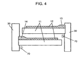
Fig. 4 is a sectional view of a conventional metallized film capacitor using a PP film. The capacitor comprises two sheets ofPP film 11 and metal-sprayedportions 30. Each of the two sheets ofPP film 11 hasmetal 12 deposited on one side thereof, and are overlaid and wound or laminated. Metal-sprayedportions 30 are formed by spraying metal from both edge faces of the capacitor. - Widely employed structure of deposited
metal 12 is a heavy edge structure shown inFig. 4 . Depositedmetal 12 in a capacity-forming electrodes portion is thinner to improve self-healing capability and the metal contact portions with sprayedmetal portions 30 are thicker to enhance the contact strength with respect to metal-sprayedportions 30. The self-healing capability is restoring the capability of the capacitor when local dielectric breakdown has occurred in a portion of a film. Evaporation and scatter of the deposited metal around of the portion interrupts the current. Commonly used as depositedmetal 12 is aluminum, zinc, or mixtures thereof. When aluminum is used, its bonding strength with respect to metal-sprayedportions 30 is weak. Additionally, when alternating voltage is applied to the capacitor for an extended period of time, deterioration of aluminum caused by oxidation thereof decreases the capacity. Because of these problems, in recent years, deposited metal essentially consisting of zinc is used in many cases. Deposited metal made of mixtures of zinc and aluminum is also used to improve humidity resistance of zinc. - In a structure shown in
Fig.4 (hereinafter referred to as a "one-side metallized film capacitor"), two sheets of PP film each having deposited metal on one side thereof are used. Thus, each sheet requires a vacuum deposition step and this necessitates a large number of man-hours. If metal can be deposited onto both sides of a PP film (hereinafter referred to as a "both-side metallized PP film") by one vacuum deposition step and the film can be placed on a non-metallized polypropylene film having no deposited layer (hereinafter referred to as a "non-metallized PP film "), the vacuum deposition step can be saved to one half. - However, a conventional both-side metallized film capacitor has the following problems. Thus, its performance is inferior to that of a one-side metallized film capacitor.
- First problem: when the conventional both-side metallized film capacitor is charged at low temperature or room temperature for an extended period of time, partial discharge occurs in an air gap between the films and deterioration develops. For a one-side metallized film capacitor, voltage is applied to each of the films via one layer of air gap. In contrast, for the both-side metallized film capacitor, the both-side metallized PP film has no air gap; however, the non-metallized PP film has air gaps on both sides. Thus, deterioration caused by partial discharge develops on both sides of the non-metallized PP film. Therefore, the deterioration develops at low temperature or room temperature at which partial discharge is prone to occur.
- Second problem: the conventional both-side metallized film capacitor has weak contact with metal-sprayed portions. In general, for metallized film capacitors, heat aging is performed to complete the heat shrinkage of the film after metal-sprayed portions are formed at both edge faces of the capacitor element. This heat aging process is performed at high temperature to alleviate the residual stress and strain produced when the film is drawn lengthwise and widthwise in a two-way drawing step and to stabilize the dimension of the film by heat shrinkage.
- When the film is shrunken widthwise in the heat aging process, stress occurs between metal-sprayed
portion 30 and contact portion of depositedelectrode 13. However, for the one-side metallized film capacitor ofFig. 4 , each of the films is in contact with the metal-sprayed portion only at one edge and thus the stress is extremely small. In contrast, for the both-side metallized film capacitor, the both-side metallized film is in contact with the metal-sprayed portions at both edges. Thus, large stress occurs at both edges and the contact portions are prone to deteriorate. Especially, heat shrinkage of polypropylene (PP) film is larger than that of a polyethylene terephthalate film, polyphenylene terephthalate film, and polyethylene naphthalate film. Thus, a PP film is prone to cause contact failure in metal-sprayed portions. - Third problem: in the case of a capacitor element impregnated or filled with insulating
oil 70, the insulating oil permeating into a both-side metallized film swells the film. Thus cracks or peels of the deposited metal occur and the resistance of the deposited layer increases. Especially, a PP film has an adhesive strength with respect to the deposited layer smaller than that of other films and insulating oil is more permeable into PP films. Therefore, increase in the resistance of the deposited layer deteriorates tan δ and deterioration of the deposited layers in the vicinity of metal-sprayed portions deteriorates contact. - Forth problem: the conventional both-side metallized film capacitor is prone to cause insulation breakdown when over voltage is applied thereto. In order to improve adhesion of a PP film to a deposited layer, it is widely performed that wettability of the surface of the PP film is improved by corona treatment in production of the PP film. In general, in the corona treatment, a drawn film runs in corona discharge generated at high voltages ranging from several thousands to several dozens of thousands volts so that the surface of the film is activated. However, a PP film having a small thickness of approx. several micrometers for use in a capacitor is damaged by the corona treatment and thus dielectric strength thereof decreases. The PP film for use in a capacitor has a large number of projections and depressions. When both sides of such a film are metallized, the thickness distribution of the film has direct influence on the dielectric strength of the capacitor. Therefore, because a portion of the film having depressions on both sides is thin, the dielectric strength of the capacitor decreases. On the other hand, for a one-side metallized film capacitor, even if the film has depressions, always existing air gaps alleviate the voltage applied to the films. For this reason, the dielectric strength of the one-side metallized film capacitor is higher than that of the both-side metallized film capacitor.
- Fifth problem: in production of a both-side metallized film, the deposited layers are peeled by blocking. After deposited layers are formed on both sides of the film in vacuum deposition step, the both-side metallized film is wound once in a vacuum evaporator. At this time, the deposited layers on both sides are in contact with each other. A PP film has low adhesive strength with respect to a deposited metal. Additionally, the roll formed after vacuum deposition is tightly contracted (i.e. the stress accumulating inside of the roll of the both-side metallized PP film is large). Thus, deposited metal layers on both sides adhere to and peel each other. This phenomenon is called blocking. It is known that the blocking is remarkable with a deposited metal of zinc.
- To address this problem, trials of decreasing blocking when zinc is deposited on both sides of a PP film have conventionally been made. For example, the
U.S. Patent Publication No. 3,895,129 discloses a method of depositing zinc on both sides of a PP film. In this invention, after the deposited surface on one side is air-sprayed to oxidize the deposited metal surface, the film is wound into a product roll. The Japanese Patent Examined Publication No.H07-24251 - However, even in the case using the method disclosed in the
U.S. Patent Publication No. 3,895,129 , blocking is not completely eliminated. It is known that observations with an optical microscope and the like show the existence of a small peeled area of deposited layer in some cases. - In other words, because blocking is caused by the contraction of a roll of both-side metallized PP film as described above, the deposited layer may peel in the inner circumference of the roll where the stress caused by the contraction accumulates even when no blocking is seen in the outer circumference of the roll. Especially increasing the tension on the PP film at vacuum deposition increases the contraction. Thus, blocking in the inner circumference is prone to increase.
- Further, because blocking is a phenomenon in which deposited layers adhere to and peel each other during unwinding, it is known that the adhesion of the deposited layers develops and the peeled area increases when the film is kept for an extended period of time in the state of the roll.
- When a capacitor is produced using a both-side metallized PP film in which blocking occurs, peeling of the deposited electrodes not only decreases the effective area but also affects the electrical characteristics as a capacitor in some cases. Especially in the heavy edge structure having thicker electrodes in the metal contact portions with sprayed metal, the deposited electrodes in the capacity-forming electrodes portion are thin. For this reason, even when a small area of the electrodes peels, the resistance of the deposited electrodes significantly increases and the capability of the electrodes is lost. Therefore, tan δ (dielectric loss) increases and the characteristics inherent to a metallized PP capacitor, i.e. a small loss, cannot be obtained.
- Further, when zinc is deposited on both sides of a PP film and an aluminum layer is formed on the deposited metal as described in the Japanese Patent Unexamined Publication No.
H07-24251 -
DE 2802769 discloses a metallized film capacitor with a PP foil metallized on both sides and a PP dielectric foil.JP 1151 221 A - To address these problems, a production process of a metallized film capacitor of the present invention uses a non-metallized polypropylene (PP) film having a lengthwise heat shrinkage factor at 120 °C of at least 4%.
- As another means of addressing these problems, in the production process of a metallized film capacitor of the present invention, a both-side metallized film having a deposited metal formed on both sides of a first polypropylene (PP) film and a second PP film are wound or laminated so as to be opposed to each other. The first PP film has a widthwise heat shrinkage factor at 120 °C of at most 1.0%.
-
-
Fig. 1 is a schematic section of an exemplary embodiment of the present invention, illustrating how films thereof are opposed to each other. -
Fig. 2 is a schematic section of another exemplary embodiment of the present invention, illustrating how films thereof are opposed to each other. -
Fig. 3 is a schematic section of still another exemplary embodiment of the present invention, illustrating how films thereof are opposed to each other. -
Fig. 4 is a schematic section of a conventional art, illustrating how films thereof are opposed to each other. -
Fig. 5 is a schematic section of another conventional art, illustrating how films thereof are opposed to each other. -
Fig. 6 is a graph showing a relation between a rate of a peeled area of a deposited metal layer and a resistance. - The present invention is specifically described with reference to the accompanying drawings.
- As shown in
Fig. 1 , a metallized film capacitor of the present invention includes first polypropylene (PP)film 10,second PP film 20, metal-sprayedportions 30, depositedelectrodes margins metal - In the metallized film capacitor of the present invention,
second PP film 20 shown inFig. 1 has a lengthwise heat shrinkage factor at 120 °C of at least 4%. Thus, the lengthwise shrinkage of the second PP film, i.e. a combination film, is sufficiently large in a heat aging step after metal-sprayedportions 30 are provided. This can decrease air gaps existing on both sides ofsecond PP film 20 and damages thereto caused by corona discharge at low temperature. As a result, deterioration of the capacitor when it is charged at low temperature or room temperature for an extended period of time can be prevented. - As shown in
Fig. 1 , the metallized film capacitor of the present invention has depositedelectrodes first PP film 10.First PP film 10 has a widthwise heat shrinkage factor at 120 °C of at most 1.0%. This can reduce the widthwise stress on the both-side metallized film in the heat aging step after metal-sprayedportions 30 are provided. As a result, occurrence of contact failure between the deposited electrodes and metal-sprayedportions 30 can be inhibited. - Further, in the metallized film capacitor of the present invention,
first PP film 10 is thicker thansecond PP film 20. This structure can prevent a decrease in the withstand voltage of the capacitor caused by projections and depressions on the both-side metallized film even when a film thinner than conventional one is used. Additionally, it is preferable that maximum surface roughness Rmax offirst PP film 10 andsecond PP film 20 ranges from 1 to 2 µm and average surface roughness Ra is at least 0.1 µm (Rmax and Ra being measured according to JISB0601). It is also preferable thatfirst PP film 10 is 0.5 to 2 µm thicker thansecond PP film 20. - In the metallized film capacitor of the present invention, the rate of the peeled area of the deposited layer in the capacity-forming electrodes portion is up to 4%, on each side of both-side metallized
PP film 10. This can realize an excellent metallized film capacitor free from deterioration of tan δ or thermal runaway caused by blocking, which is one of the problems. The methods of reducing the rate of the peeled area of the deposited layer in the capacity-forming electrodes portion to 4% or smaller include spraying oxygen onto the deposited layer. However, this embodiment is not limited to this method and any other method can be used for this purpose. - In the metallized film capacitor of the present invention, the membrane resistance of the capacity-forming electrodes portion (deposited
electrodes 41 and 42) is higher than that of the electrode lead (metal contact portions with sprayedmetal 61 and 62) on each of depositedelectrodes side metallized film 10 This can provide excellent contact of metal-sprayedportions 30 with the deposited electrodes. - In the metallized film capacitor of the present invention, each of deposited
electrodes - In the metallized film capacitor of the present invention, each of deposited
electrodes - With reference to
Fig. 1 , in each of depositedelectrodes portions 30. - Next, another embodiment of the present invention is described with reference to
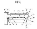
Fig. 2 . - The metallized film capacitor shown in
Fig. 2 includes first polypropylene (PP)film 10,second PP film 20, metal-sprayedportions 30, depositedelectrodes margins metal - In the metallized film capacitor of the present invention, deposited
electrodes PP film 10,and depositedelectrode 43 is formed at one edge offirst PP film 10 where insulatingmargin 52 is formed on depositedelectrode 42. Because of this structure, metal-sprayedportions 30 connect to depositedmetal metal portions 30 and can maintain stable contact of the metal-sprayed portions even in heat cycles, e.g. heat generation in operation and cooling at rest, during use of the capacitor. - In the case of a capacitor impregnated or filled with insulating
oil 70 in the entire part thereof, the deposited metal is effective in inhibiting entry of insulatingoil 70 intofirst PP film 10 in the vicinity of metal-sprayedportions 30. This can prevent deterioration of tan δ and contact in use of insulating oil, which is one of the problems. - Further, still another exemplary embodiment of the present invention is described with reference to
Fig. 3 . -
Fig. 3 shows that a metallized film capacitor includes first polypropylene (PP)film 10,second PP film 20, metal-sprayedportions 30, depositedelectrodes margins metal second PP film 20 is disposed in contact with depositedelectrode 43 at the edge on the side of insulatingmargin 52. This arrangement prevents direct contact ofPP film 10 i.e. the base of the both-side metallized film, with insulatingoil 70. Thus, preventing entry of the insulating oil is more effective. - In
Fig. 3 , a gap is shown betweensecond PP film 20 and depositedelectrode 43 at the edge on the side of insulatingmargin 52 for a better understanding. However, in fact,second PP film 20 is in intimate contact with depositedelectrode 43 and the entire surface of insulatingmargin 52 and a part of depositedelectrode 43 are covered withPP film 20. - For the metallized film capacitor of the present invention, with reference to
Fig. 3 , one side ofsecond PP film 20 is not subjected to corona treatment and the other side is subjected to corona treatment. This can prevent damage tosecond PP film 20 caused by corona treatment and decrease in dielectric strength while excellent adherence between the second PP film and the deposited layers is maintained. - Examples and conventional examples are produced for each of these exemplary embodiments and the experimental results thereof are detailed hereinafter.
- In Example 1, after aluminum is formed, as a seed metal, on both sides of first polypropylene (PP)
film 10 having a thickness of 6 µm and a widthwise heat shrinkage factor at 120 °C of at most 1.0%, deposited layers are formed so that a high resistance portion corresponding to the capacity-forming electrodes portion has a resistance of 15±3Ω/□ and metal contact portions with sprayedmetal margins electrodes second PP film 20 is a PP film having the same thickness of 6 µm and a lengthwise heat shrinkage factor at 120 °C of at least 4% and subjected to no corona treatment. The second film is 79mm wide. The both-side metallized film and the non-metallized film, i.e.second PP film 20, prepared in this manner are wound so that thesecond film 20 is placed in the center of the both-side metallized film 10. This makes the amount of displacement between both edges offirst PP film 10 and both edges of second PP film 20 (hereinafter referred to as "displacement") 1mm at each edge face. Insulatingmargins PP film 20. After winding, Zn is sprayed onto both edge faces. - Example 2 is produced by using a PP film having a widthwise heat shrinkage factor at 120 °C of 1.5%, as a first PP film. The other structure is the same as that of Example 1.
- Example 3 is produced by using a PP film having a lengthwise heat shrinkage factor at 120 °C of 3%, as
second PP film 20. The other structure is the same as that of Example 1. - In Example 4-1, deposited
electrodes margins second PP film 20 is only a part of each of insulatingmargins - In Example 4-2, deposited
electrode 43 at the edge on the side of an insulating margin is provided only on one side offirst PP film 10 and the opposite side of the PP film does not have a deposited electrode at the edge. The other structure is the same as that of Example 4-1. - In Example 5-1,
second PP film 20 is 77 mm wide and placed in the center of a both-side metallized film and wound together. The other structure is the same as that of Example 1. Thus, the displacement is 2 mm and only a part of each of insulatingmargins second PP film 20. - In Example 5-2,
second PP film 20 is 78 mm wide and placed in a position 1 mm displaced from the center of a both-side metallized film and wound together. The other structure is the same as that of Example 1. In this case, the displacement is 2 mm at one edge and 1mm at the other edge. Thus, one insulating margin is completely covered with the second PP film; however, only a part of the other insulating margin is covered with the film. - In Example 6-1, both sides of
second PP film 20 are subjected to corona treatment. The other structure is the same as that of Example 1. - In Example 6-2, only one side of
second PP film 20 is subjected to corona treatment. The other structure is the same as that of Example 1. - For Conventional Example 1, a conventional one-side metallized capacitor is produced. After aluminum is formed, as a seed metal, on one side of 6-µm-
thick PP film 11 subjected to corona treatment on one side, a deposited layer is formed so that a high resistance portion has a resistance of 15±3Ω/□ and metal contact portions with sprayed metal have a resistance of 5±2Ω/□. Insulating margins are 3 mm wide and the film is 80 mm wide. After the one-side metallized films prepared in this manner are wound together so that the two films are displaced by 1 mm, Zn is sprayed onto both edge faces. The other structure is the same as that of Example 1. - All of these examples and conventional examples are wound capacitors in which two films are overlaid and wound together. The electrostatic capacity of each capacitor is 30 µF.
- Evaluation is performed by comparing the measurement of tan δ at 1 kHz in the initial state with the measurement of tan δ at 1 kHz after 50 cycles. One cycle is made with no voltage applied at 0 °C for two hours and with 400VAC applied at 80 °C for two hours. For comparison of withstand voltage, step-up tests are performed at temperature of 25 °C and 70 °C. In each of the step-up tests, alternating voltage is increased from 800 V by 50 V within 10 minutes and break-down voltage is measured.
- The obtained results are shown in Table 1.
Table 1 Widthwise heat shrinkage factor of at most 1.0% Length wise heat shrinkage factor of at least 4% Deposited electrode at end of margin *1 Contact with deposited electrode *1 Corona Treatment *2 Tan at 1 δ kHz voltage in step-up Break-down test Initial state After heat cycles Room Temperatur 70°C Examples 1 Yes Yes B B B 0.40% 0.40% 1200 V 1100 V Example 2 No Yes B B B 0.4% ~0.6% 0.4% ~1.2 % 1100 V 1100 V Example 3 Yes No B B B 0.40% 0.40% 1000 V 1100 V Example 4-1 Yes Yes × × B 0.40% 1.20% 1200 V 1100 V Example 4-2 Yes Yes A × B 0.40% 0.80% 1200 V 1100 V Example 5-1 Yes Yes B × B 0.40% 0.65% 1200 V 1100 V Example 5-2 Yes Yes B A B 0.40% 0.50% 1200 V 1100 V Example 6-1 Yes Yes B B × 0.40% 0.40% 1050 V 950V Example 6-2 Yes Yes B B A 0.40% 0.40% 1100 V 1000 V Conventional Example 1 0.40% 1.20% 1200 V 1100 V *1: B: at both ends, A: at one end, ×: at no end
*2: B: both sides, A: one side, ×: no corona treatment - Comparison of Example 1, Example 2, and Conventional Example 1 shows that use of a first PP film having a widthwise heat shrinkage factor at 120°C of at most 1.0% can reduce the widthwise stress on the both-side metallized film in a heat aging step after metal-sprayed portions are provided, and thus inhibit occurrence of contact failure of the metal-sprayed portions.
- Comparison of Example 1, Example 3, and Conventional Example 1 shows that use of a second PP film having a lengthwise heat shrinkage factor at 120°C of at least 4% can reduce air gaps existing on both sides of
second PP film 20 and damages caused by corona discharge at low temperature, and thus improve withstand voltage at low temperature. - Comparison of Example 1, Example 4-1, Example 4-2, and Conventional Example 1 shows that formation of a deposited electrode at the edge on the side of the insulating margin of at least one of deposited
electrodes first PP film 10 improves characteristics of the both-side metallized film capacitor in comparison with those of the conventional one-side metallized film capacitor. This is because formation of the deposited electrode at the edge provides mechanical connection between the sprayed metal and the deposited metal on both sides of the film and thus increases the mechanical strength of the metal-sprayed portion. Additionally, the deposited metal inhibits entry of insultingoil 70 into the PP film in the vicinity of metal-sprayed portion and thus stabilizes contact of the metal-sprayed portion even in heat cycles, e.g. heat generation in operation and cooling at rest, during use of the capacitor. - Next, Example 1, Example 5-1, Example 5-2, and Conventional Example 1 are compared with each other. Disposing the second PP film in contact with the deposited electrode at the edge on the side of the insulating margin prevents direct contact of the PP film, a base of the both-side metallized film, with insulating
oil 70. Stability of contact of the metal-sprayed portions in heat cycles is drastically improved in comparison with that of the conventional one-side metallized film capacitor. - Comparison of Example 1, Example 6-1, Example 6-2, and Conventional Example 1 shows that the withstand voltage is substantially equal to that of the conventional one-side metallized film capacitor when at least one side of
second PP film 20 is not subjected to corona treatment. - The following other examples and conventional examples are produced in accordance with the exemplary embodiment of the present invention and the experimental results thereof are detailed.
- For Example 7, a metallized film capacitor structured as shown in
Fig. 1 is produced by windingfirst PP film 10 having a thickness of 7 µm andsecond PP film 20 having a thickness of 6.5 µm together. For both films, maximum surface roughness Rmax is 1.5 µm and average surface roughness Ra is 0.1 µm. Rmax and Ra are measured according to JISB0601. - For Example 8, a metallized film capacitor structured as shown in
Fig. 1 is produced by usingsecond PP film 20 having a thickness of 5 µm. The other structure is the same as that of Example 7. - For Example 9, a metallized film capacitor as shown in
Fig. 1 is produced by usingfirst PP film 10 having a thickness of 7.5 µm. The other structure is the same as that of Example 7. - For Conventional Example 2, a metallized film capacitor as shown in
Fig. 5 is produced by windingfirst PP film 100 andsecond PP film 200 each having a thickness of 7 µm and a maximum surface roughness Rmax of 2.5 µm in a manner similar to that of Example 7. - For Conventional Example 3, a metallized film capacitor structured as shown in
Fig. 4 is produced by winding two sheets of one-side metallized PP film 7 µm thick in pairs. - Table 2 shows the withstand voltage of the capacitors, i.e. Examples 7 through 9, and Conventional Examples 2 and 3. Measured as the withstand voltage is break-down voltage in a test in which alternating voltage is incremented by 50V and each voltage is maintained for five minutes.
- The results are shown in Table 2.
Table 2 Thickness of first film (both-side metallized film) (µm) Thickness of second film (No deposited metal) (µm) Thickness of one-side metallized film (µm) Withstand voltage (V) Example 7 7 6.5 - 1050 Example 8 7 5 - 1050 Example 9 7.5 6.5 - 1250 Comparative Example 7 4.5 800 Conventional Example 2 7 7 - 1050 Conventional Example 3 - - 7 1250 - Although the capacitor of Example 7 has a second PP film 0.5 µm thinner than that of Conventional Example 2, these two examples have the same withstand voltage of 1,050V. Because
second PP film 20 has air gaps on both sides, the withstand voltage same as that of Conventional Example 2 can be obtained even with a thickness of 6.5 µm. - Although the capacitor of Example 8 has a second PP film 2 µm thinner than that of Conventional Example 2, these two examples has the same withstand voltage of 1,050V.
- This result shows that
second PP film 20 2 µm thinner thanfirst PP film 10 does not affect the withstand voltage. - As a comparative example, a capacitor including
second PP film 20 having a thickness as small as 4.5 µm is produced. In this case, the withstand voltage is as small as 800V. This result shows that it is preferable to set the difference in thickness between the first and second PP films within 2 µm when surface roughness Rmax ranges 1 to 2 µm and the average roughness is at least 0.1 µm. - In the capacitor of Example 9,
first PP film 10 is 0.5 µm thicker than that of Conventional Example 2. In this case, althoughsecond PP film 20 is 0.5 µm thinner than that of Conventional Example 2, the withstand voltage of Example 9 is improved to 1,250V.First PP film 10 of Example 9 has projections and depressions such that maximum surface roughness Rmax is 1.5 µm and average surface roughness Rà is 0.1 µm. This means there can be a portion 3 µm thinner than the other portions at maximum. Thus, increasing the thickness offirst PP film 10 by 0.5 µm can further increase the withstand voltage. - For Example 9, increasing the thickness of
first PP film 10 by 0.5 µm provides withstand voltage higher than that of Conventional Example 2 using a both-side metallized film 7 µm thick. This is the effect of thickening the first PP film. - Further, examples and conventional examples of a laminated capacitor in accordance with the exemplary embodiment of the present invention are produced. The experimental results thereof are detailed hereinafter.
- For Example 10, a metallized film capacitor as shown in
Fig. 1 is produced in the following manner. First PP film 7 µm thick and second PP film 6.5 µm thick are wound around a large-diameter core and metal-sprayedportions 30 are formed at both edge faces. Then, the wound films are cut by a metal saw to provide laminated capacitors. The sectional structure is as shown inFig. 1 . Maximum surface roughness Rmax offirst PP film 10 andsecond PP film 20 is 2 µm and average surface roughness Ra thereof is 0.2 µm. - For Example 11, a metallized film capacitor as shown in
Fig. 1 is produced so thatfirst PP film 10 is 8 µm thick andsecond PP film 20 is 6 µm thick. The other production method is the same as that of Example 10. - In Conventional Example 4, each of
first PP film 10 andsecond PP film 20 is 7 µm thick and maximum surface roughness Rmax of these PP films is 2.5 µm. The other method of producing laminated film capacitors is the same as that of Example 10. - For Conventional Example 5, laminated film capacitors are produced using two sheets of one-side metallized PP film 7 µm thick in a manner similar to that of Example 10.
- Table 3 shows the withstand voltage of the capacitors, i.e. Examples 10 and 11, and Conventional Examples 4 and 5. Measured as the withstand voltage is break-down voltage in a test in which alternating voltage is incremented by 50V and each voltage is maintained for five minutes.
Table 3 Thickness of first film (both-side metallized film) (µm) Thickness of second film (No deposited metal) (µm) Thickness of one-side metallized film (µm) Withstand voltage (V) Example 10 7 6.5 - 950 Example 11 8 6 - 1050 Conventional Example 4 7 7 - 950 Conventional Example 5 -- -- 7 1000 - The inventors have found from a large number of experiments that making the first metallized film 0.5 to 2 µm thicker than the second metallized film is effective in increasing the withstand voltage when the PP films have maximum roughness Rmax ranging from 1 to 2 µm and an average roughness of 0.1 µm.
- Although the capacitor of Example 10 has a second film 0.5 µm thinner than that of Conventional Example 4, these capacitors have the same withstand voltage of 950V. In other words, this result shows that the second film can be made 0.5 µm thinner than the first film even in a laminated capacitor.
- In the capacitor of Example 11, the first film is 1 µm thicker and the second film is 1 µm thinner than those of the capacitor of Conventional Example 4. This structure has improved the withstand voltage to 1,050V. Thickening a both-side metallized film having projections and depression can increase withstand voltage as shown in Example 11.
- In Example 11, making the first film 1 µm thicker has made the withstand voltage thereof 50V higher than that of Conventional Example 5.
- Further, the following other examples and conventional examples in accordance with the exemplary embodiment of the present invention are produced. The characteristics of each of the metallized film capacitors are described in comparison with those of the conventional examples.
- First, a metallized film capacitor as shown in
Fig. 1 is produced in the following manner. Depositedmetal first PP film 10 having a thickness of 6µm so that aluminum is a lower layer and zinc is upper layer, and the deposited layer in a capacity-forming electrodes portion has a resistance of approx. 10Ω/□ and electrode leads have a resistance of 5Ω/□. Next, by changing the time taken from vacuum deposition to slitting (time when the film is stored in the state of a roll) within the range of one hour to one week, both-side metallized PP films having different rates of the area peeled by blocking are produced. - Next, the both-side metallized PP film is slit. Then, the resistance of the deposited layer and the rate of the peeled area of the deposited layer are examined in the capacity-forming electrodes portion of each of the slit sheets. The resistance is measured with a resistance meter "Hiresta" made by the Mitsubishi Chemical Corp., according to JISK7194. The rate of the peeled area of the deposited layer is obtained by imaging the capacity-forming electrodes portion in deposited
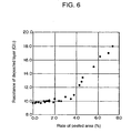
electrodes electrodes - The resistance of the deposited layer and the rate of the peeled area of the deposited layer that are obtained in the aforementioned manner are shown in Table 6. According to the results, when the rate of the peeled area is up to 4%, a resistance substantially equal to the resistance at vacuum deposition is obtained. In contrast, when the rate exceeds 4%, the resistance rapidly increases and the function as an electrode is affected.
- Next, a metallized film capacitor structured as shown in
Fig. 1 is produced using both-side metallizedPP film 10 and 6-µm-thick PP film 20 in the aforementioned manner. Then, the relation between the rate of the peeled area of depositedmetal - Table 4 also includes the images of the deposited electrodes in the capacity-forming electrodes portion taken by an optical microscope in the aforementioned manner, the rate of the peeled area, and the resistance of the deposited layer. Shown in Table 4 is a picture of the deposited surface on a primary side (the surface on which the deposited layer is formed first in a vacuum evaporator) of the both-side metallized PP film taken in the aforementioned manner. As for a secondary side (the surface on which the deposited layer is formed next in the vacuum evaporator), similar pictures are taken and the values in the table are obtained.
- Table 4 obviously show that a metallized film capacitor having a small loss can be obtained when the rate of the peeled area of deposited
electrode 
- Next, the characteristics of metallized film capacitors are examined by changing the composition of the deposited metal.
- First, a zinc-deposited layer containing one of copper, silver, and aluminum as a seed metal is formed on both sides of 4-µm-
thick PP film 10 to provide a roll of the aforementioned both-side metallized PP film. Next, sheets of the both-side metallized PP film each having different rates of the peeled area of depositedmetal Fig. 1 are produced. The relation between the rate of the peeled area of the capacity-forming electrodes portion and the dielectric loss of the capacitor is examined. The results are shown in Table 5. Examples 15 through 19 show the examples in which the rate of the peeled area is up to 4%. Conventional Examples 8 through 10 show the examples in which the rate exceeds 4%.Table 5 Seed metal Rate of peeled area (%) Dielectric loss of capacitor (%) Primary side Secondary side Example 15 Copper 0.7 0.9 0.04 Example 16 Copper 3.0 2.9 0.06 Example 17 Silver 0.5 0.6 0.04 Example 18 Silver 2.3 2.0 0.06 Example 19 Aluminum 1.2 1.4 0.05 Conventional Example 8 Copper 5.3 6.4 0.16 Conventional Example 9 Silver 4.3 4.1 0.14 Conventional Example 10 Aluminum 6.8 7.5 0.20 - Table 5 obviously shows that a metallized film capacitor having a small loss can be obtained with any seed metal when the rate of the peeled area of the capacity-forming electrodes portion is up to 4%.
- Next, cases using two-layer deposited electrodes of aluminum and zinc are examined in detail. As the exemplary embodiment of the present invention, metallized film capacitors each structured as shown in
Fig. 1 orFig. 2 are produced using 6-µm-thick both-side metallized PP film that has depositedelectrodes Fig. 5 is produced using a both-side metallized PP film that has a rate of the peeled area exceeding 4%. Additionally, a metallized film capacitor structured as shown inFig. 4 is produced using two sheets of one-side metallized PP film placed one on another. Further, as shown in the Japanese Patent Unexamined Publication No.H07-24251 Fig.5 is produced using a both-side metallized PP film that has a zinc-deposited layer containing copper as a seed metal and an aluminum layer formed on the zinc layer on both sides thereof. - Charge-discharge tests are performed on these
capacitors 20 times to measure the dielectric loss thereof. In the charge-discharge test, the capacitor is charged to 900VDC and forcedly short-circuited using a copper plate. Table 6 shows the results. In this case, Examples 20 through 22 show the cases where the rate of peeled area is up to 4% and Conventional Examples 11 through 13 show the cases where the rate exceeds 4%. - Comparison between Examples 20, 21, and 22 and Conventional Example 11 shows that providing deposited
metal Fig. 2 in a metallized film capacitor having a rate of the peeled area in the capacity-forming electrodes portion up to 4% improves contact of the deposited electrodes with metal-sprayedportions 30 and thus provide a current-resistant capacitor exhibiting less deterioration in charge-discharge tests. - For Conventional Example 12 (one-side metallized) and Conventional Example 13 (aluminum upper layer), because no deposited metal peels, the dielectric loss in the initial state is low; however, poor contact of the deposited metal with the metal- sprayed portions increases the dielectric loss after the charge-discharge tests. In contrast, for Examples 21 and 22, the dielectric loss does not increase significantly.
- Also, when one of copper, silver, and aluminum is used as a seed metal of the deposited metal, providing deposited
electrodes Table6 Deposited metal (upper layer / lower layer) Structure Rate of peeled area (%) Dielectric loss of capacitor (%) Primary side Secondary side Initial state After tests Example 20 Al/Zn Fig. 2 0.5 0.3 0.04 0.05 Example 21 Al/Zn Fig. 2 3.0 2.9 0.06 0.07 Example 22 Al/Zn Fig. 1 0.3 0.2 0.04 0.09 Conventional Example 11 Al/Zn Fig. 5 5.0 4.8 0.14 0.18 Conventional Example 12 Al/Zn (one side) Fig. 4 0.0 0.0 0.03 0.09 Conventional Example 13 Cu/Zn/Al Fig. 5 0.0 0.0 0.03 0.24 - As described above, a metallized film capacitor of the present invention uses a non-metallized polypropylene (PP) film having a lengthwise heat shrinkage factor at 120 °C of at least 4%. Thus, the capacitor element significantly shrinks in a heat aging step and air gaps decrease. Because this inhibits partial discharge, deterioration caused when a capacitor is charged for an extended period of time at low temperature or room temperature, which is a first problem, can significantly be prevented.
- In the present invention, a PP film, i.e. a base of a both-side metallized PP film, has a widthwise heat shrinkage factor at 120 °C of at most 1.0%. This reduces the widthwise stress on the both-side metallized film in the step of heat-aging the element. Thus, poor contact with metal-sprayed portions, which is a second problem, can be improved.
- Further in the present invention, a deposited electrode is formed at the edge of an insulating margin of a deposited electrode at least one side of the both-side metallized PP film. Thus, mechanical connection between a metal-sprayed portion and a deposited metal is provided on both sides of the film. This further increases the mechanical strength of the metal-sprayed portion and stabilizes contact with the metal-sprayed portion even in heat cycles, e.g. heat generation in operation and cooling at rest, during the use of the capacitor.
- Additionally, the second PP film is disposed in contact with the deposited electrode at the edge of the insulating margin formed on the first PP film that has metal electrodes on both sides. This prevents direct contact of insulating oil with the first PP film and thus the deposited metal can inhibit entry of the insulating oil into the first PP film. Thus, deterioration of tan δ and contact, which is a third problem, can be prevented.
- At least one side of the second PP film is not subjected to corona treatment. This decreases damages to the surface of the film caused by corona treatment. Thus, decrease in dielectric strength, which is a fourth problem, can be inhibited.
- Further, the both-side metallized PP film is made thicker than the second PP film. This can prevent decrease in the withstand voltage of the capacitor caused by projections and depressions on the both-side metallized PP film.
- In the present invention, the rate of the peeled area of the deposited layer in the capacity-forming electrodes portion is up to 4% on each side of the both-side metallized PP film. This can realize an excellent metallized film capacitor free from deterioration of tan δ and thermal runaway caused by blocking, which is a fifth problem.
- Additionally, the membrane resistance of the deposited electrode in the capacity-forming electrodes portion is higher than that of the electrode lead on each side of the metallized film capacitor. This improves contact with the metal-sprayed portions.
- Further, the deposited electrodes are made of zinc containing one of copper, silver, and aluminum, as a seed metal thereof. This composition can realize a preferable metallized film capacitor free from decrease in capacity even when alternating voltage is applied for an extended period of time.
-
- 10
- First polypropylene film
- 20
- Second polypropylene film
- 30
- Metal-sprayed portion
- 11
- polypropylene (PP) film
- 12
- Deposited electrode
- 13,14
- Metal contact portion with sprayed metal
- 41,42,43,44
- Deposited electrode
- 51,52
- Insulating margin
- 61,62
- Metal contact portion with sprayed metal
- 70
- Insulating oil
- 100
- First polypropylene film of conventional art
- 200
- Second polypropylene film of conventional art
Claims (8)
- A production process of a metallized film capacitor comprising a capacitor element, the capacitor element being made by one of winding and laminating a first polypropylene (PP) film (10) having metal deposited electrodes (41,42) on both sides thereof, and a second PP film opposed to the first PP film, comprising the steps of:providing a first polypropylene (PP) film (10) wherein a widthwise heat shrinkage factor at 120°C of the first PP film (10) is at most 1%;depositing metal electrodes (41,42) on both sides of the first PP film (10);providing a second PP film (20) wherein a lengthwise heat shrinkage factor at 120°C of the second PP film (20) is at least 4%;winding or laminating the first PP film (10) and the second PP film (20);forming metal-sprayed portions (30) at both edge faces of the capacitor element;performing a heat aging step of the capacitor element after the metal-sprayed portions (30) are provided.
- The production process of claim 1, wherein lead electrodes (61,62) in the deposited electrodes in a vicinity of the metal-sprayed portions (30) have a membrane resistance smaller than that of the capacity-forming electrodes portion.
- The production process of claim 1, further comprising a seed metal deposited on the first PP film (10), wherein the seed metal is one of silver, copper, and aluminum.
- The production process of anyone of claims 1 through 3, wherein one of the deposited electrodes on at least one side of the first PP film (10) has an insulating margin (51) at one edge, and another deposited electrode (44) is provided at an edge on a side of the insulating margin (51).
- The production process of claim 1, wherein one of the deposited electrodes (41,42) on at least one side of the first PP film (10) has an insulating margin (52) at one edge, and another deposited electrode (43) is provided at an edge on a side of the insulating margin (52), and the second PP film (20) is disposed in contact with the deposited electrode (43) formed at the one edge of the insulating margin (52) on the first PP film (10).
- The production process of claim 1, wherein the first PP film (10) is thicker than the second PP film (20).
- The production process of claim 6, wherein both of the first PP film (10) and the second PP film (20) have maximum surface roughness Rmax ranging from 1 to 2 µm and average surface roughness Ra of at least 0.1 µm, and a difference in thickness between the first PP film (10) and the second PP film (20) ranges from 0.5 to 2 µm.
- The production process of anyone of claims 1 through 3, wherein each of the deposited electrodes (41,42) has a two-layer structure including an aluminum layer deposited as a lower layer and a zinc layer deposited as an upper layer.
Applications Claiming Priority (7)
| Application Number | Priority Date | Filing Date | Title |
|---|---|---|---|
| JP2001173663 | 2001-06-08 | ||
| JP2001173677A JP3858626B2 (en) | 2001-06-08 | 2001-06-08 | Double-sided metallized film capacitor |
| JP2001173677 | 2001-06-08 | ||
| JP2001173663A JP3608530B2 (en) | 2001-06-08 | 2001-06-08 | Film capacitor |
| JP2001267270A JP3767436B2 (en) | 2001-09-04 | 2001-09-04 | Metallized film capacitors |
| JP2001267270 | 2001-09-04 | ||
| PCT/JP2002/005592 WO2002101770A1 (en) | 2001-06-08 | 2002-06-06 | Metallized film capacitor |
Publications (3)
| Publication Number | Publication Date |
|---|---|
| EP1400992A1 EP1400992A1 (en) | 2004-03-24 |
| EP1400992A4 EP1400992A4 (en) | 2007-10-17 |
| EP1400992B1 true EP1400992B1 (en) | 2011-08-17 |
Family
ID=27346898
Family Applications (1)
| Application Number | Title | Priority Date | Filing Date |
|---|---|---|---|
| EP02733341A Expired - Lifetime EP1400992B1 (en) | 2001-06-08 | 2002-06-06 | Production process of a metallized film capacitor |
Country Status (4)
| Country | Link |
|---|---|
| US (1) | US6954349B2 (en) |
| EP (1) | EP1400992B1 (en) |
| CN (1) | CN1311485C (en) |
| WO (1) | WO2002101770A1 (en) |
Cited By (1)
| Publication number | Priority date | Publication date | Assignee | Title |
|---|---|---|---|---|
| DE102014202067B4 (en) * | 2014-02-05 | 2016-11-24 | Siemens Aktiengesellschaft | film capacitor |
Families Citing this family (23)
| Publication number | Priority date | Publication date | Assignee | Title |
|---|---|---|---|---|
| EP2157589B1 (en) * | 2001-06-08 | 2012-06-27 | Panasonic Corporation | Method of manufacturing double surface metallized film. |
| US9154906B2 (en) | 2002-03-28 | 2015-10-06 | Telecommunication Systems, Inc. | Area watcher for wireless network |
| JP3914854B2 (en) * | 2002-10-10 | 2007-05-16 | 松下電器産業株式会社 | Metalized film capacitor, inverter smoothing capacitor and automotive capacitor using the same |
| CN1298527C (en) * | 2004-12-31 | 2007-02-07 | 浙江南洋电子薄膜有限公司 | Thermostable biaxially oriented polypropylene film adapted for high power capacitor and its making method |
| KR100867038B1 (en) * | 2005-03-02 | 2008-11-04 | 삼성전기주식회사 | Printed circuit board with embedded capacitors, and manufacturing process thereof |
| EP1868216B1 (en) | 2005-04-08 | 2014-01-01 | Panasonic Corporation | Metalized film capacitor and inverter smoothing capacitor for automobile |
| US20070084043A1 (en) * | 2005-10-14 | 2007-04-19 | Sb Electronics | Conductive Adhesive Attachment of Capacitor Terminals |
| JP4698474B2 (en) * | 2006-04-28 | 2011-06-08 | 双信電機株式会社 | Film capacitor |
| US7471499B2 (en) * | 2006-06-30 | 2008-12-30 | Electronic Concepts, Inc | Wound capacitor providing a thermal alert of a hot spot |
| DE112008003150T5 (en) * | 2008-01-07 | 2010-09-30 | Siemens Aktiengesellschaft | Capacitor for use in high-pressure environments |
| US8451133B2 (en) * | 2009-08-07 | 2013-05-28 | Electronic Concepts, Inc. | Large current carrying capacitor having a thermal disconnect with a light indicator |
| CN103366958A (en) * | 2013-07-08 | 2013-10-23 | 华中科技大学 | High-voltage metallized film capacitor |
| US10784049B2 (en) * | 2014-02-03 | 2020-09-22 | Lg Chem, Ltd. | Winding-type stacked body for condenser with high electrostatic capacitance and stacked winding-type condenser using the same |
| CN105097284B (en) * | 2014-12-16 | 2018-11-13 | 安徽格太信控科技有限公司 | Capacitor metalized film |
| CN105826075B (en) * | 2016-04-28 | 2018-09-18 | 长兴蓝天电子有限公司 | A kind of frequency converter metallic film filter condenser |
| WO2018079150A1 (en) * | 2016-10-28 | 2018-05-03 | パナソニックIpマネジメント株式会社 | Film capacitor |
| US20180374647A1 (en) * | 2017-06-27 | 2018-12-27 | Scientific Applications & Research Associates, Inc. | Pulsed metallized film capacitor |
| CN108155010A (en) * | 2017-12-13 | 2018-06-12 | 河南华佳新材料技术有限公司 | A kind of two-sided metallization polypropylene film and preparation method thereof |
| JP7143674B2 (en) * | 2018-08-08 | 2022-09-29 | 日新電機株式会社 | metallized film and film capacitors |
| CN110233049B (en) * | 2019-05-27 | 2022-09-02 | 广东明路电力电子有限公司 | Folding capacitor core and processing technology thereof |
| CN110684944A (en) * | 2019-09-29 | 2020-01-14 | 浙江七星电子股份有限公司 | Double-sided aluminum metalized polypropylene film, preparation method thereof and capacitor core |
| CN114868215A (en) * | 2019-12-20 | 2022-08-05 | 京瓷株式会社 | Thin film capacitor element and thin film capacitor |
| CN113628880A (en) * | 2021-07-02 | 2021-11-09 | 中国船舶重工集团公司第七一三研究所 | Internal series self-healing metallized film and capacitor |
Citations (1)
| Publication number | Priority date | Publication date | Assignee | Title |
|---|---|---|---|---|
| JPH04280617A (en) * | 1991-03-08 | 1992-10-06 | Toray Ind Inc | Polypropylene film for double-side vapor deposition |
Family Cites Families (18)
| Publication number | Priority date | Publication date | Assignee | Title |
|---|---|---|---|---|
| US3714528A (en) * | 1972-01-13 | 1973-01-30 | Sprague Electric Co | Electrical capacitor with film-paper dielectric |
| US3895129A (en) | 1973-02-20 | 1975-07-15 | Sprague Electric Co | Method for metallizing plastic film |
| JPS5228221B2 (en) | 1973-05-21 | 1977-07-25 | ||
| US3900775A (en) * | 1974-06-24 | 1975-08-19 | Matsushita Electric Ind Co Ltd | Metallized film capacitor |
| DE2802769A1 (en) * | 1978-01-23 | 1979-07-26 | Roederstein Kondensatoren | Multilayer film capacitor - with polypropylene foil metallised on both sides and polypropylene dielectric |
| JPS5940519A (en) | 1982-08-30 | 1984-03-06 | 岡谷電機産業株式会社 | Metallized film condenser |
| JPH01151221A (en) * | 1987-12-08 | 1989-06-14 | Matsushita Electric Ind Co Ltd | Manufacture of both-face metallized film capacitor |
| JPH02138721A (en) * | 1988-11-18 | 1990-05-28 | Matsushita Electric Ind Co Ltd | Metallized film capacitor |
| JPH02285618A (en) | 1989-04-26 | 1990-11-22 | Nichicon Corp | Metallized plastic film capacitor |
| JPH085779B2 (en) | 1989-09-22 | 1996-01-24 | 杏林製薬株式会社 | Fleroxacin eye drops |
| JPH03234010A (en) * | 1990-02-09 | 1991-10-18 | Matsushita Electric Ind Co Ltd | Metallized film capacitor |
| JPH03109326U (en) * | 1990-02-22 | 1991-11-11 | ||
| FR2664022B1 (en) | 1990-06-28 | 1995-06-16 | Inst Francais Du Petrole | METHOD AND DEVICE FOR GENERATING HEAT COMPRISING DESULFURIZATION OF EFFLUENTS WITH FINE SIZE ABSORBENT PARTICLES IN A TRANSPORTED BED. |
| US5610796A (en) * | 1993-02-19 | 1997-03-11 | Electronic Concepts, Inc. | Metallized capacitor having increased dielectric breakdown voltage and method for making the same |
| JP3654541B2 (en) * | 1995-11-29 | 2005-06-02 | 東レ株式会社 | Polypropylene film for heat-resistant capacitors |
| JPH11260662A (en) | 1998-03-06 | 1999-09-24 | Toray Ind Inc | Polypropylene film for oil-impregnated capacitor and capacitor constituted of the film |
| JPH11288842A (en) * | 1998-04-03 | 1999-10-19 | Matsushita Electric Ind Co Ltd | Metallized film capacitor |
| JP2001106804A (en) * | 1999-10-12 | 2001-04-17 | Oji Paper Co Ltd | Polypropylene film for both surface-depositing |
-
2002
- 2002-06-06 WO PCT/JP2002/005592 patent/WO2002101770A1/en active Application Filing
- 2002-06-06 EP EP02733341A patent/EP1400992B1/en not_active Expired - Lifetime
- 2002-06-06 CN CNB028020243A patent/CN1311485C/en not_active Expired - Lifetime
- 2002-06-06 US US10/479,957 patent/US6954349B2/en not_active Expired - Lifetime
Patent Citations (1)
| Publication number | Priority date | Publication date | Assignee | Title |
|---|---|---|---|---|
| JPH04280617A (en) * | 1991-03-08 | 1992-10-06 | Toray Ind Inc | Polypropylene film for double-side vapor deposition |
Cited By (1)
| Publication number | Priority date | Publication date | Assignee | Title |
|---|---|---|---|---|
| DE102014202067B4 (en) * | 2014-02-05 | 2016-11-24 | Siemens Aktiengesellschaft | film capacitor |
Also Published As
| Publication number | Publication date |
|---|---|
| CN1311485C (en) | 2007-04-18 |
| US6954349B2 (en) | 2005-10-11 |
| EP1400992A4 (en) | 2007-10-17 |
| EP1400992A1 (en) | 2004-03-24 |
| US20040232465A1 (en) | 2004-11-25 |
| CN1463452A (en) | 2003-12-24 |
| WO2002101770A1 (en) | 2002-12-19 |
Similar Documents
| Publication | Publication Date | Title |
|---|---|---|
| EP1400992B1 (en) | Production process of a metallized film capacitor | |
| US8213159B2 (en) | Electrode foil, method of manufacturing electrode foil, and electrolytic capacitor | |
| JP5708586B2 (en) | Multilayer ceramic electronic component and manufacturing method thereof | |
| EP2157589B1 (en) | Method of manufacturing double surface metallized film. | |
| US5844770A (en) | Capacitor structures with dielectric coated conductive substrates | |
| US20130286538A1 (en) | Multilayer ceramic electronic component and method of manufacturing the same | |
| US3991451A (en) | Method of making a fluoride film capacitor | |
| JP4915947B2 (en) | Metallized film capacitors | |
| US10460876B2 (en) | Multi-layer ceramic capacitor | |
| EP3857582B1 (en) | Film capacitor with coated acrylic dielectric layer inside | |
| US20230034387A1 (en) | Multilayer ceramic capacitor | |
| JP2007194310A (en) | Solid electrolytic capacitor, and method of manufacturing same | |
| JP3190177B2 (en) | Manufacturing method of multilayer ceramic chip capacitor | |
| EP2400514A1 (en) | Capacitor and method for manufacturing capacitor | |
| JP3767436B2 (en) | Metallized film capacitors | |
| US20120075769A1 (en) | High temperature high current metalized film capacitor | |
| JPH11186090A (en) | Capacitor and metallized dielectric for the capacitor | |
| JP7143674B2 (en) | metallized film and film capacitors | |
| JP2002043165A (en) | Heat-radiating mechanism in electronic component | |
| JPH11251175A (en) | Capacitor | |
| JP2002121298A (en) | Polyphenylene sulfide film and capacitor | |
| JPS63224313A (en) | Metallized plastic film capacitor | |
| JPS62213228A (en) | Manufacture of film capacitor | |
| JP2003224030A (en) | Method of manufacturing laminated ceramic electronic component | |
| JP2004153206A (en) | Polyphenylene sulfide film roll for deposition and capacitor |
Legal Events
| Date | Code | Title | Description |
|---|---|---|---|
| PUAI | Public reference made under article 153(3) epc to a published international application that has entered the european phase |
Free format text: ORIGINAL CODE: 0009012 |
|
| 17P | Request for examination filed |
Effective date: 20031203 |
|
| AK | Designated contracting states |
Kind code of ref document: A1 Designated state(s): AT BE CH CY DE DK ES FI FR GB GR IE IT LI LU MC NL PT SE TR |
|
| A4 | Supplementary search report drawn up and despatched |
Effective date: 20070918 |
|
| RAP1 | Party data changed (applicant data changed or rights of an application transferred) |
Owner name: PANASONIC CORPORATION |
|
| 17Q | First examination report despatched |
Effective date: 20081223 |
|
| GRAP | Despatch of communication of intention to grant a patent |
Free format text: ORIGINAL CODE: EPIDOSNIGR1 |
|
| RTI1 | Title (correction) |
Free format text: PRODUCTION PROCESS OF A METALLIZED FILM CAPACITOR |
|
| GRAS | Grant fee paid |
Free format text: ORIGINAL CODE: EPIDOSNIGR3 |
|
| GRAA | (expected) grant |
Free format text: ORIGINAL CODE: 0009210 |
|
| AK | Designated contracting states |
Kind code of ref document: B1 Designated state(s): DE IT |
|
| REG | Reference to a national code |
Ref country code: DE Ref legal event code: R096 Ref document number: 60240803 Country of ref document: DE Effective date: 20111020 |
|
| PLBE | No opposition filed within time limit |
Free format text: ORIGINAL CODE: 0009261 |
|
| STAA | Information on the status of an ep patent application or granted ep patent |
Free format text: STATUS: NO OPPOSITION FILED WITHIN TIME LIMIT |
|
| 26N | No opposition filed |
Effective date: 20120521 |
|
| REG | Reference to a national code |
Ref country code: DE Ref legal event code: R097 Ref document number: 60240803 Country of ref document: DE Effective date: 20120521 |
|
| PGFP | Annual fee paid to national office [announced via postgrant information from national office to epo] |
Ref country code: IT Payment date: 20150625 Year of fee payment: 14 |
|
| PG25 | Lapsed in a contracting state [announced via postgrant information from national office to epo] |
Ref country code: IT Free format text: LAPSE BECAUSE OF NON-PAYMENT OF DUE FEES Effective date: 20160606 |
|
| PGFP | Annual fee paid to national office [announced via postgrant information from national office to epo] |
Ref country code: DE Payment date: 20180522 Year of fee payment: 17 |
|
| REG | Reference to a national code |
Ref country code: DE Ref legal event code: R119 Ref document number: 60240803 Country of ref document: DE |
|
| PG25 | Lapsed in a contracting state [announced via postgrant information from national office to epo] |
Ref country code: DE Free format text: LAPSE BECAUSE OF NON-PAYMENT OF DUE FEES Effective date: 20200101 |