EP1398755A2 - Plasma display panel apparatus and method for driving the same - Google Patents
Plasma display panel apparatus and method for driving the same Download PDFInfo
- Publication number
- EP1398755A2 EP1398755A2 EP03090172A EP03090172A EP1398755A2 EP 1398755 A2 EP1398755 A2 EP 1398755A2 EP 03090172 A EP03090172 A EP 03090172A EP 03090172 A EP03090172 A EP 03090172A EP 1398755 A2 EP1398755 A2 EP 1398755A2
- Authority
- EP
- European Patent Office
- Prior art keywords
- current
- inductor
- conductive pattern
- voltage
- panel capacitor
- Prior art date
- Legal status (The legal status is an assumption and is not a legal conclusion. Google has not performed a legal analysis and makes no representation as to the accuracy of the status listed.)
- Withdrawn
Links
Images





Classifications
-
- G—PHYSICS
- G09—EDUCATION; CRYPTOGRAPHY; DISPLAY; ADVERTISING; SEALS
- G09G—ARRANGEMENTS OR CIRCUITS FOR CONTROL OF INDICATING DEVICES USING STATIC MEANS TO PRESENT VARIABLE INFORMATION
- G09G3/00—Control arrangements or circuits, of interest only in connection with visual indicators other than cathode-ray tubes
- G09G3/20—Control arrangements or circuits, of interest only in connection with visual indicators other than cathode-ray tubes for presentation of an assembly of a number of characters, e.g. a page, by composing the assembly by combination of individual elements arranged in a matrix no fixed position being assigned to or needed to be assigned to the individual characters or partial characters
- G09G3/22—Control arrangements or circuits, of interest only in connection with visual indicators other than cathode-ray tubes for presentation of an assembly of a number of characters, e.g. a page, by composing the assembly by combination of individual elements arranged in a matrix no fixed position being assigned to or needed to be assigned to the individual characters or partial characters using controlled light sources
- G09G3/28—Control arrangements or circuits, of interest only in connection with visual indicators other than cathode-ray tubes for presentation of an assembly of a number of characters, e.g. a page, by composing the assembly by combination of individual elements arranged in a matrix no fixed position being assigned to or needed to be assigned to the individual characters or partial characters using controlled light sources using luminous gas-discharge panels, e.g. plasma panels
- G09G3/288—Control arrangements or circuits, of interest only in connection with visual indicators other than cathode-ray tubes for presentation of an assembly of a number of characters, e.g. a page, by composing the assembly by combination of individual elements arranged in a matrix no fixed position being assigned to or needed to be assigned to the individual characters or partial characters using controlled light sources using luminous gas-discharge panels, e.g. plasma panels using AC panels
- G09G3/296—Driving circuits for producing the waveforms applied to the driving electrodes
-
- G—PHYSICS
- G09—EDUCATION; CRYPTOGRAPHY; DISPLAY; ADVERTISING; SEALS
- G09G—ARRANGEMENTS OR CIRCUITS FOR CONTROL OF INDICATING DEVICES USING STATIC MEANS TO PRESENT VARIABLE INFORMATION
- G09G3/00—Control arrangements or circuits, of interest only in connection with visual indicators other than cathode-ray tubes
- G09G3/20—Control arrangements or circuits, of interest only in connection with visual indicators other than cathode-ray tubes for presentation of an assembly of a number of characters, e.g. a page, by composing the assembly by combination of individual elements arranged in a matrix no fixed position being assigned to or needed to be assigned to the individual characters or partial characters
- G09G3/22—Control arrangements or circuits, of interest only in connection with visual indicators other than cathode-ray tubes for presentation of an assembly of a number of characters, e.g. a page, by composing the assembly by combination of individual elements arranged in a matrix no fixed position being assigned to or needed to be assigned to the individual characters or partial characters using controlled light sources
- G09G3/28—Control arrangements or circuits, of interest only in connection with visual indicators other than cathode-ray tubes for presentation of an assembly of a number of characters, e.g. a page, by composing the assembly by combination of individual elements arranged in a matrix no fixed position being assigned to or needed to be assigned to the individual characters or partial characters using controlled light sources using luminous gas-discharge panels, e.g. plasma panels
- G09G3/288—Control arrangements or circuits, of interest only in connection with visual indicators other than cathode-ray tubes for presentation of an assembly of a number of characters, e.g. a page, by composing the assembly by combination of individual elements arranged in a matrix no fixed position being assigned to or needed to be assigned to the individual characters or partial characters using controlled light sources using luminous gas-discharge panels, e.g. plasma panels using AC panels
- G09G3/296—Driving circuits for producing the waveforms applied to the driving electrodes
- G09G3/2965—Driving circuits for producing the waveforms applied to the driving electrodes using inductors for energy recovery
-
- G—PHYSICS
- G09—EDUCATION; CRYPTOGRAPHY; DISPLAY; ADVERTISING; SEALS
- G09G—ARRANGEMENTS OR CIRCUITS FOR CONTROL OF INDICATING DEVICES USING STATIC MEANS TO PRESENT VARIABLE INFORMATION
- G09G2300/00—Aspects of the constitution of display devices
- G09G2300/04—Structural and physical details of display devices
- G09G2300/0404—Matrix technologies
- G09G2300/0408—Integration of the drivers onto the display substrate
-
- G—PHYSICS
- G09—EDUCATION; CRYPTOGRAPHY; DISPLAY; ADVERTISING; SEALS
- G09G—ARRANGEMENTS OR CIRCUITS FOR CONTROL OF INDICATING DEVICES USING STATIC MEANS TO PRESENT VARIABLE INFORMATION
- G09G2310/00—Command of the display device
- G09G2310/06—Details of flat display driving waveforms
-
- G—PHYSICS
- G09—EDUCATION; CRYPTOGRAPHY; DISPLAY; ADVERTISING; SEALS
- G09G—ARRANGEMENTS OR CIRCUITS FOR CONTROL OF INDICATING DEVICES USING STATIC MEANS TO PRESENT VARIABLE INFORMATION
- G09G2330/00—Aspects of power supply; Aspects of display protection and defect management
- G09G2330/02—Details of power systems and of start or stop of display operation
- G09G2330/021—Power management, e.g. power saving
- G09G2330/023—Power management, e.g. power saving using energy recovery or conservation
- G09G2330/024—Power management, e.g. power saving using energy recovery or conservation with inductors, other than in the electrode driving circuitry of plasma displays
-
- G—PHYSICS
- G09—EDUCATION; CRYPTOGRAPHY; DISPLAY; ADVERTISING; SEALS
- G09G—ARRANGEMENTS OR CIRCUITS FOR CONTROL OF INDICATING DEVICES USING STATIC MEANS TO PRESENT VARIABLE INFORMATION
- G09G2330/00—Aspects of power supply; Aspects of display protection and defect management
- G09G2330/06—Handling electromagnetic interferences [EMI], covering emitted as well as received electromagnetic radiation
-
- G—PHYSICS
- G09—EDUCATION; CRYPTOGRAPHY; DISPLAY; ADVERTISING; SEALS
- G09G—ARRANGEMENTS OR CIRCUITS FOR CONTROL OF INDICATING DEVICES USING STATIC MEANS TO PRESENT VARIABLE INFORMATION
- G09G3/00—Control arrangements or circuits, of interest only in connection with visual indicators other than cathode-ray tubes
- G09G3/20—Control arrangements or circuits, of interest only in connection with visual indicators other than cathode-ray tubes for presentation of an assembly of a number of characters, e.g. a page, by composing the assembly by combination of individual elements arranged in a matrix no fixed position being assigned to or needed to be assigned to the individual characters or partial characters
- G09G3/22—Control arrangements or circuits, of interest only in connection with visual indicators other than cathode-ray tubes for presentation of an assembly of a number of characters, e.g. a page, by composing the assembly by combination of individual elements arranged in a matrix no fixed position being assigned to or needed to be assigned to the individual characters or partial characters using controlled light sources
- G09G3/28—Control arrangements or circuits, of interest only in connection with visual indicators other than cathode-ray tubes for presentation of an assembly of a number of characters, e.g. a page, by composing the assembly by combination of individual elements arranged in a matrix no fixed position being assigned to or needed to be assigned to the individual characters or partial characters using controlled light sources using luminous gas-discharge panels, e.g. plasma panels
- G09G3/288—Control arrangements or circuits, of interest only in connection with visual indicators other than cathode-ray tubes for presentation of an assembly of a number of characters, e.g. a page, by composing the assembly by combination of individual elements arranged in a matrix no fixed position being assigned to or needed to be assigned to the individual characters or partial characters using controlled light sources using luminous gas-discharge panels, e.g. plasma panels using AC panels
- G09G3/291—Control arrangements or circuits, of interest only in connection with visual indicators other than cathode-ray tubes for presentation of an assembly of a number of characters, e.g. a page, by composing the assembly by combination of individual elements arranged in a matrix no fixed position being assigned to or needed to be assigned to the individual characters or partial characters using controlled light sources using luminous gas-discharge panels, e.g. plasma panels using AC panels controlling the gas discharge to control a cell condition, e.g. by means of specific pulse shapes
- G09G3/293—Control arrangements or circuits, of interest only in connection with visual indicators other than cathode-ray tubes for presentation of an assembly of a number of characters, e.g. a page, by composing the assembly by combination of individual elements arranged in a matrix no fixed position being assigned to or needed to be assigned to the individual characters or partial characters using controlled light sources using luminous gas-discharge panels, e.g. plasma panels using AC panels controlling the gas discharge to control a cell condition, e.g. by means of specific pulse shapes for address discharge
- G09G3/2932—Addressed by writing selected cells that are in an OFF state
Definitions
- the present invention relates to a plasma display panel (PDP). More specifically, the present invention relates to an address driver circuit for applying an address voltage.
- PDP plasma display panel
- the PDP is advantageous over the other flat panel displays in regard to its high luminance, high luminous efficiency, and wide view angle, and accordingly, it is favorable for making large-scale screen of more than 40 inches assubstitute for the conventional cathode ray tube (CRT).
- CTR cathode ray tube
- the PDP is a flat panel display that uses plasma generated by gas discharge to display characters or images and includes, according to its size, more than several scores to millions of pixels arranged in a matrix pattern.
- Such a PDP is classified into a direct current (DC) type and an alternating current (AC) type according to its discharge cell structure and the waveform of the driving voltage applied thereto.
- the DC-type PDP has electrodes exposed to a discharge space, allowing a DC to flow through the discharge space while voltage is applied, and hence requires resistors for limiting the current.
- the AC-type PDP has electrodes covered with a dielectric layer that naturally forms a capacitance component that limits the current and protects the electrodes from the impact of ions during a discharge.
- the AC-type PDP is superior to the DC-type PDP in regard to long lifetime.
- the AC type-PDP has scan and sustain electrodes and address electrodes.
- the scan and sustain electrodes are formed in parallel with each other on one side of the PDP, and the address electrodes are formed on the other side of the PDP and are perpendicular to the scan and sustain electrodes.
- the sustain electrodes are formed in correspondence to the scan electrodes with one terminal thereof commonly coupled to one terminal of each scan electrode.
- the driving method of the AC-type PDP is sequentially composed of a reset step, an addressing step, a sustain discharge step, and an erase step.
- the state of each cell is initialized in order to readily perform an addressing operation on the cell.
- an address voltage is applied to accumulate wall charges on selected "on"-state cells and other "on"-state cells (i.e., addressed cells) for selecting "off'-state cells on the panel.
- a sustain discharge voltage pulse is applied so as to cause a discharge that actually displays an image on the addressed cells.
- the wall charges on the cells are erased to end the sustain discharge.
- the discharge spaces formed between the scan and sustain electrodes and between the address electrode side and the scan/sustain electrode side act as capacitive load (hereinafter referred to as "panel capacitor") so that capacitance exists on the panel. Due to the capacitance of the panel capacitor, a reactive power is required in addition to the addressing power in order to apply a waveform for an addressing operation.
- the address driver circuit for a PDP includes a power recovery circuit for recovering the reactive power and reusing it. The power recovery circuits are suggested in USP. Nos. 4,866,349 and 5,081,400 by L. F. Weber.
- a conductive output pattern running in the transverse direction of the address buffer board may cause a parasitic inductance component.
- a plurality of address driving ICs are required for driving the address electrodes, because all the address electrodes cannot be coupled to a single address driving IC.
- the parasitic inductance component is possibly formed on the output pattern in which the address driving ICs are coupled to the address buffer board.
- the parasitic inductance component causes an extreme distortion on the address driving waveform. Namely, an undesired pulse rise may occur in the rise/drop interval of the address driving waveform because of the parasitic inductance component.
- a power recovery circuit for recovering a reactive power and reusing it, and minimizing the effect of a parasitic inductance component present in an address driver circuit.
- the present invention stores energy in both an inductor and a parasitic inductance component and uses the stored energy and an LC resonance for charging/discharging a panel capacitor.
- an apparatus for driving a PDP which applies a voltage to a panel capacitor that is coupled on a conductive pattern formed lengthwise.
- the apparatus includes an inductor coupled to one terminal of the conductive pattern.
- First and second switches are coupled to the inductor, and operated to charge and discharge the panel capacitor to first and second voltages, respectively.
- a third switch is coupled between another terminal of the conductive pattern and a first power source for supplying the first voltage, and is operated to generate a current of a first direction flowing to the conductive pattern and the inductor.
- a fourth switch is coupled between the other terminal of the conductive pattern and a second power source for supplying the second voltage, and is operated to generate a current of a second direction flowing to the inductor and the conductive pattern, the second direction being opposite to the first direction.
- a power line is coupled to the first and second switches and supplies a voltage having a value between the first and second voltages.
- the panel capacitor is discharged to the second voltage by a resonance between the inductor and the panel capacitor while the current of the first direction is flowing.
- the panel capacitor is charged to the first voltage by a resonance between the inductor and the panel capacitor while the current of the second direction is flowing.
- an apparatus for driving a plasma display panel which receives first and second voltages from first and second power sources, respectively, and applies a voltage to a panel capacitor coupled on a conductive pattern formed lengthwise.
- the apparatus includes a power line for supplying a voltage having a value between the first and second voltages.
- An inductor has one terminal thereof coupled to one terminal of the conductive pattern.
- a first current path is formed to make a current of a first direction flow to the inductor and the conductive pattern, when another terminal of the conductive pattern is coupled to the second power source.
- a second current path is formed to charge the panel capacitor to the first voltage, when a resonance between the inductor and the panel capacitor is generated while the current of the first direction is flowing.
- a third current path is formed to recover the current of the first direction remaining in the inductor and the conductive pattern, while the panel capacity is sustained at the first voltage.
- a fourth current path is formed to make a current of a second direction flow to the conductive pattern and the inductor, when the other terminal of the conductive pattern is coupled to the first power source, the second direction being opposite to the first direction.
- a fifth current path is formed to discharge the panel capacitor to the second voltage, when a resonance between the inductor and the panel capacitor is formed while the current of the second direction is flowing.
- a sixth current path is formed to recover the current of the second direction remaining in the inductor and the conductive pattern, while the panel capacitor is sustained at the second voltage.
- a method for driving a plasma display panel which receives first and second voltages from first and second power sources, respectively, and applies a voltage to a panel capacitor coupled on a conductive pattern formed lengthwise.
- a current of a first direction is applied to the conductive pattern and an inductor is coupled to one terminal of the conductive pattern.
- a resonance is generated between the panel capacitor and the inductor to charge the panel capacitor to the first voltage, while the current of the first direction is flowing to the conductive pattern and the inductor.
- the current remaining in the inductor and the conductive pattern is recovered while sustaining the panel capacitor at the first voltage.
- a current of a second direction is applied to the inductor and the conductive pattern, the second direction being opposite to the first direction.
- a resonance is generated between the panel capacitor and the inductor to discharge the panel capacitor to the second voltage, while the current of the second direction is flowing to the inductor and the conductive pattern.
- the current remaining in the inductor and the conductive pattern is recovered while sustaining the panel capacitor at the second voltage.
- a plasma display panel apparatus includes a plurality of address electrodes, a plurality of scan and sustain electrodes arranged in pairs and parallel with one another, and a panel capacitor formed among the address, scan, and sustain electrodes.
- a driver circuit supplies a driving signal to the scan, sustain, and address electrodes.
- the driver circuit includes: a conductive pattern formed lengthwise and coupled to one of the address, scan, and sustain electrodes; an inductor coupled to one terminal of the conductive pattern; a first current injecting means coupled to the other terminal of the conductive pattern and applying a current of a first direction to the inductor and the conductive pattern while sustaining the panel capacitor at a first voltage; a discharging means for generating a resonance between the inductor and the panel capacitor to discharge the panel capacitor to a second voltage, while the current of the first direction is flowing to the inductor and the conductive pattern by way of the first current injecting means; a second current injecting means for applying a current of a second direction to the inductor and the conductive pattern while sustaining the panel capacitor at a second voltage, the second direction being opposite to the first direction; and a charging means for generating a resonance between the inductor and the panel capacitor to charge the panel capacitor to the first voltage, while the current of the second direction is flowing to the inductor and the conductive pattern by way of the
- a plasma panel includes a first substrate, a plurality of address electrodes formed on the first substrate, a second substrate being opposite to the first substrate, and a plurality of scan and sustain electrodes formed on the second substrate and arranged in pairs and parallel with one another.
- a sash base is provided opposite to the plasma display panel and includes an address buffer board for transferring a driving signal to the address electrodes, and a scan and sustain driver board for transferring the driving signal to the scan and sustain electrodes.
- the address buffer board includes: a printed circuit board; an output pattern formed lengthwise on one side of the printed circuit board and coupled to the address electrodes; an inductor formed on the printed circuit board and coupled to one terminal of the output pattern; first and second switches formed on the printed circuit board and coupled to the inductor; and third and fourth switches formed on the printed circuit board and coupled to the other terminal of the output pattern.
- the currents of the first and second directions include a freewheeling current, a current formed by a voltage difference, or both.
- a resonance can also be generated between a parasitic inductance component present in the conductive pattern and the panel capacitor.
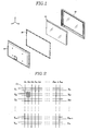
- Fig. 1 is an exploded perspective of a PDP apparatus according to an embodiment of the present invention.
- Fig. 2 is a schematic plane view of a PDP according to an embodiment of the present invention.
- Fig. 3 is a schematic plane view of a sash base according to an embodiment of the present invention.
- the PDP apparatus includes, as shown in Fig. 1, plasma panel 10, sash base 20, front case 30, and rear case 40.
- Sash base 20 is arranged on the side of plasma panel 10 opposite the image displaying side and is coupled to plasma panel 10.
- Front and rear cases 30 and 40 are arranged on the front side of plasma panel 10 and on the back side of sash base 20 and are coupled to plasma panel 10 and sash base 20, respectively, thereby completing a PDP apparatus.
- plasma panel 10 includes a plurality of address electrodes A 1 to A m arranged in columns, and a plurality of scan electrodes Y 1 to Y n and sustain electrodes X 1 to X n alternately arranged in rows. Sustain electrodes X 1 to X n are formed in correspondence to scan electrodes Y 1 to Y n , respectively, with one terminal of each sustain electrode generally being coupled to one terminal of each scan electrode.
- Plasma panel 10 also includes a glass substrate on which sustain and scan electrodes X 1 to X n and Y 1 to Y n are arranged, and a glass substrate on which address electrodes A 1 to A m are arranged.
- the two glass substrates are disposed opposite to each other, with a discharge space formed between them such that scan electrodes Y 1 to Y n and sustain electrodes X 1 to X n are orthogonal to address electrodes A 1 to A m .
- a discharge space at each intersection of address electrodes A 1 to A m and sustain and scan electrodes X 1 to X n and Y 1 to Y n form discharge cell 11.
- boards 100 to 600 that are necessary for driving plasma panel 10 are formed on sash base 20.
- An address buffer board 100 is formed on the upper and lower parts of sash base 20 and may be composed of a single board or a plurality of boards. Although a dual-drive plasma display panel apparatus is exemplified in Fig. 3, address buffer board 100 for a single-drive plasma display panel apparatus is disposed on either of an upper or lower part of sash base 20.
- Address buffer board 100 receives an address drive control signal from picture-processing and logic board 500, and it applies a voltage for selecting discharge cells to be displayed to respective address electrodes A 1 to A m .
- Scan and sustain driver boards 200 and 300 are arranged on the left and right sides of sash base 20, respectively.
- Scan board 200 is coupled to scan electrodes Y 1 to Y n via scan buffer board 400.
- Scan buffer board 400 performs an operation necessary for the scanning of scan electrodes Y 1 to Y n .
- Scan and sustain driver boards 200 and 300 receive a sustain discharge signal from picture-processing and logic board 500, and apply a sustain discharge pulse alternately to scan and sustain electrodes Y 1 to Y n and X 1 to X n .
- a sustain discharge occurs on the discharge cells selected by the sustain discharge pulse application.
- scan and sustain driver boards 200 and 300 are separately described in Fig. 3, the two boards 200 and 300 can be implemented as a single board, and scan buffer board 400 can also be integrated with scan driver board 200.
- Picture-processing and logic board 500 receives an externally applied picture signal to generate an address drive control signal and a sustain discharge signal, and applies the address drive control signal and the sustain discharge signal to address buffer board 100 and scan and sustain driver boards 200 and 300, respectively.
- Power supply board 600 supplies power necessary for driving the plasma display panel apparatus. Picture-processing and logic board 500 and power supply board 600 are arranged in the center of sash base 200.
- address driver circuit 110 included in address driver board 100 will be described in detail with reference to Figs. 4 and 5 and Figs. 6A to 6H.
- Fig. 4 is a schematic circuit diagram of an address driver circuit according to an embodiment of the present invention.
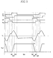
- Fig. 5 is a timing diagram showing a driving operation of the address driver circuit according to an embodiment of the present invention.
- Figs. 6A to 6H are illustrations showing a current path in each mode of the address driver circuit according to an embodiment of the present invention.
- Address driver circuit 110 is coupled to address electrodes A 1 to A m via a plurality of address buffer ICs.
- Conductive output pattern 116 in which the address buffer ICs are coupled to address buffer board 100 functions as a parasitic inductance component.
- Address electrodes A 1 to A m formed on plasma panel 10 together with other electrodes Y 1 to Y n and X 1 to X n function as a capacitive load, which is generally called a "panel capacitor".
- the voltage for addressing in address driver circuit 110 is applied only to the discharge cells selected by the address buffer ICs.
- the address buffer ICs are not shown but the parasitic inductance components are equivalently expressed as parasitic inductors L p1 , L p2 , and L p3 on the assumption that address voltage V a is applied to two panel capacitors.
- a voltage high enough to select discharge cells with a voltage between both terminals of the panel capacitor is applied to the other terminal of the panel capacitor to which address voltage V a is applied.
- the voltage is assumed as ground voltage 0V in Fig. 4.
- Address driver circuit 110 includes, as shown in Fig. 4, resonance circuit 112 and output circuit 114 coupled to each other with parasitic inductors L p1 , L p2 , and L p3 disposed between them.
- Panel capacitors C p1 and C p2 are coupled between a contact of parasitic inductors L p1 and L p2 and ground terminal O and between a contact of parasitic inductors L p2 and L p3 and ground terminal O, respectively.
- Clamping diodes D c1 and D c2 are also coupled between contacts of parasitic inductors L p1 , L p2 , and L p3 and a power source V A for supplying address voltage V a , respectively.
- Clamping diodes D c1 and D c2 prevent the voltage of panel capacitors C p1 and C p2 from exceeding address voltage V a in an actual circuit.
- Resonance circuit 112 includes power recovery capacitor C r , switches A r and A f , an inductor L, and freewheeling diodes D f1 and D f2 .
- Output circuit 114 includes switches A a and A g .
- Other active elements for making a freewheeling current flow to power source V A or ground terminal O can also be used instead of freewheeling diodes D f1 and D f2 .
- switches A r , A f , A a , and A g are denoted as MOSFETs in Fig. 4, they can be any switching elements so long as they perform the same or similar functions.
- switches A r , A f , A a , and A g have a body diode such as a pn junction separated structure of semiconductor lCs.
- inductor L is coupled to parasitic inductor L p1
- freewheeling diode D f1 is coupled between inductor L and power source V A
- freewheeling diode D f2 is coupled between inductor L and ground terminal O, respectively.
- Switches A r and A f are coupled in parallel between inductor L and capacitor C r , capacitor C r being coupled to ground terminal O.
- Capacitor C r acts as a power source for supplying voltage V a /2 that amounts to approximately half address voltage V a .
- diodes D 1 and D 2 for interrupting a current flowing to the body diode of switches A r and A f can be formed between inductor L and capacitor C r .
- Switches A r and A f act as means for charging and discharging panel capacitors C p1 and C p2 .
- switches A a and A g are coupled in series between power source V A and ground terminal O, and their contact is coupled to parasitic inductor L p3 .
- Switches A a and A g act as a means for injecting a current to inductor L and parasitic inductors L p1 , L p2 , and L p3 prior to a charge/discharge of panel capacitors C p1 and C p2 .
- Voltages V p1 and V p2 of panel capacitors C p1 and C p2 have a similar output waveform, excepting a difference caused by the effect of parasitic inductor L p2 . Accordingly, only voltage V p1 of panel capacitor C p1 is shown in Fig. 5.
- capacitor C r is charged to voltage V a /2 amounting to half the address voltage V a and that switch A g is turned on to form a freewheeling current flowing to a path of freewheeling diode D f2 , inductor L, parasitic inductors L p1 , L p2 , and L p3 , and switch A g .
- the voltage of panel capacitor C p1 and C p2 is sustained at 0V.
- switch A r In mode 1 (M1), with switch Ag on, switch A r is turned on, as shown in Fig. 5. Then, a current path that includes capacitor C r , switch A r , diode D 1 , inductor L, parasitic inductors L p1 , L p2 , and L p3 , switch A g , and ground terminal O is formed as shown in Fig. 6A so as to inject a current to inductor L and parasitic inductors L p1 , L p2 , and L p3 . Particularly, this current is injected while the freewheeling current is flowing prior to mode 1 (M1), so that current I L flowing to inductor L is linearly increased from a predetermined value.
- switch A g is turned off. Then, a current path that includes capacitor C r , switch A r , diode D 1 , inductor L, parasitic inductor L p1 , panel capacitor C p1 or parasitic inductor L p2 , and panel capacitor C p2 is formed as shown in Fig. 6B to generate an LC resonance.
- the LC resonance current flows while a predetermined amount of current is flowing to inductor L and parasitic inductors L p1 and L p2 , so that panel capacitors C p1 and C p2 are charged for a short time.
- an unwanted pulse rise does not occur as in the prior art, because parasitic inductors L p1 and L p2 are used to generate the LC resonance while a current is injected to parasitic inductors L p1 and L p2 beforehand. Voltages V p1 and V p2 of the panel capacitors are not increased to above address voltage V a due to the body diode of switch A a or clamping diodes D c1 and D c2 . The current applied to parasitic inductor L p3 is recovered to power source V A via the body diode of switch A a .
- switch A a is turned on when voltages V p1 and V p2 of panel capacitors C P1 and C P2 are increased to address voltage V a .
- voltages V p1 and V p2 of panel capacitors C p1 and C p2 are sustained at address voltage V a , and current l L flowing to inductor L is recovered to power source V A via parasitic inductors L p1 , L p2 , and L p3 and the body diode of switch A a .
- mode 4 switch A r is turned off when current l L flowing to inductor L is recovered, as shown in Fig. 5. Then, a freewheeling current is generated on inductor L and parasitic inductors L p1 , L p2 , and L p3 in the opposite direction of current in modes 1, 2, and 3 (M1, M2, and M3), as shown in Fig. 6D.
- the freewheeling current flows to power source V A via freewheeling diode D f1 . Due to this freewheeling current, the current is injected to inductor L and parasitic inductors L P1 , L P2 , and L P3 .
- mode 5 In mode 5 (M5), with switch A a on, switch A f is turned on. Then, a current path that includes power source V A , switch A a , parasitic inductors L p3 , L p2 , and L p1 , inductor L, diode D 2 , switch A f , and capacitor C r is formed as shown in Fig. 6E so as to inject a current in the opposite direction of the current in mode 1 (M1) to inductor L and parasitic inductors L p1 , L p2 , and L p3 . Particularly, this current is injected while the freewheeling current is flowing, so that the magnitude of current l L flowing to inductor L is linearly increased from a predetermined value.
- switch A a is turned off for a discharge of panel capacitors C p1 and C p2 . Then, the energy charged in panel capacitors C p1 and C p2 is recovered to capacitor C r via parasitic inductor L p1 , inductor L, diode D 2 , and switch A f due to the LC resonance caused by panel capacitors C p1 and C p2 , inductor L and parasitic inductor L p1 and/or L p2 , as shown in Fig. 6F.
- the LC resonance current flows while a predetermined amount of current is flowing to inductor L and parasitic inductors L p1 and L p2 , so that panel capacitors C p1 and C p2 are discharged for a short time. Also, an unwanted pulse rise does not occur as in the prior art, because parasitic inductors L p1 and L p2 are used to generate the LC resonance while a current is applied to parasitic inductors L p1 and L p2 beforehand.
- switch A g is turned on when voltages V p1 and V p2 of panel capacitors C p1 and C p2 are decreased to 0V.
- voltages V p1 and V p2 of panel capacitors C p1 and C p2 are sustained at 0V due to ground terminal O.
- Current l L flowing to inductor L is recovered to capacitor C r via a current path that includes the body diode of switch Ag, parasitic inductors L p3 , L p2 and L p1 , inductor L, diode D 2 , and switch A f .
- switch A f is turned off when current l L flowing to inductor L is recovered. Then, a freewheeling current is generated through freewheeling diode D f2 , inductor L, parasitic inductors L p1 , L p2 , and L p3 , and switch A g . Namely, the freewheeling current is generated in the opposite direction of current in modes 4 to 7 (M4 - M7). Due to this freewheeling current, the current is applied to inductor L and parasitic inductors L p1 , L p2 , and L p3 .
- the current is previously applied to the inductor and the parasitic inductance components formed on the output pattern, and the inductor and the parasitic inductance components are used for LC resonance while the current is injected. It is therefore possible to eliminate a rise pulse that may otherwise occur when the panel capacitors are charged/discharged due to the parasitic inductance components.
- the charge/discharge time, i.e., the rise/drop time of the panel capacitor voltages can also be reduced, because the LC resonance occurs after the current is applied beforehand.
- the current is applied to the inductor and the parasitic inductors using both a freewheeling current generated after a current recovery and a current generated from the voltage difference.
- a freewheeling current generated after a current recovery can be used.
- either of the freewheeling current or the current generated from the voltage difference can be used.
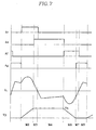
- Figs. 7 and 9 are timing diagrams showing a driving operation of an address driver circuit according to another embodiment of the present invention
- Fig. 8 is a schematic circuit diagram of the address driver circuit according to another embodiment of the present invention.
- the driving timing according to another embodiment of the present invention is the same as that shown in Fig. 5, except that modes 1 and 5 (M1 and M5) are excluded. More specifically, the current is injected to the inductor and the parasitic inductors only with a freewheeling current generated in modes 4 and 8 (M4 and M8), and the LC resonance is caused while the freewheeling current is flowing, thereby charging/discharging panel capacitors C p1 and C p2 .
- the voltage difference between power source V A or the ground terminal and capacitor C r is used to generate a current applied to the inductor and the parasitic inductors. Accordingly, as shown in Fig. 8, freewheeling diodes D f1 and D f2 can be eliminated in the address driver circuit according to this embodiment. As shown in Fig. 9, the driving timing according to this embodiment is the same as that shown in Fig. 5, except that the freewheeling current does not flow to inductor L.
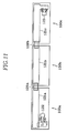
- address buffer board 100 having address driver circuit 110 will be described in detail with reference to Figs. 10 and 11.
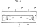
- Figs. 10 and 11 are schematic plane views of the address buffer board according to an embodiment of the present invention.
- inductor L is disposed on the left side of printed circuit board 120 of address buffer board 100, and switches A r and A f are disposed on the right side to inductor L and coupled to inductor L.
- Inductor L is coupled to switches A a and A g via an output pattern 121 formed on printed circuit board 120.
- Drivers 122 and 123 for driving switches A r and A f and switches A a and A g , respectively, are formed around these switches.
- Output pattern 121 is formed in the transverse direction on printed circuit board 120 and actually functions as parasitic inductors L p1 , L p2 , and L p3 .
- Output pattern 121 is generally formed on the reverse side of printed circuit board 120, but in Fig. 10, it is expediently shown on the upper side of the printed circuit board.
- Flexible printed circuit (FPC) board 124 is coupled to printed circuit board 120 of address buffer board 100, and also to address electrodes A 1 to A m .
- the above-stated address buffer ICs are mounted on FPC board 124 in the form of chips. This is called a “chip on flexible (COF) board system”.
- the address buffer ICs may be mounted directly on the printed circuit board of address buffer board 100. This is called a “chip on board (COB) system”.
- Address buffer board 100 arranged on the upper or lower part of sash base 20 can be composed of a single board or a plurality of boards.
- address driver circuit 110 can be mounted on individual address buffer boards 100.
- inductor L and switches A r and A f are formed on left-handed address buffer board 100a among plural address buffer boards 100, and switches A a and A g are formed on right-hand address buffer board 100c.
- Connectors 126a and 126b are coupled between output patterns 121 a and 121 b of address buffer boards 100a and 100b and between output patterns 121 b and 121 c of address buffer boards 100b and 100c, respectively.
- inductor L is coupled to switches A a and A g via output patterns 121 a, 121 b, and 121 c of address buffer boards 100a, 100b, and 100c.
- separate address driver circuit 110 may be mounted on the upper and lower address driver boards.
- inductor L and switches A r and A f are mounted on either one of the upper or lower address driver boards 100, and switches A a and A g are mounted on the other address driver board 100.
- inductor L and switches A r , A f , A a , and A g are arranged such that inductor L is coupled to switches A a and A g via the output pattern of upper and lower address buffer boards 100.
- embodiments of the present invention are applied to the address buffer board, they can also be applied to the output pattern formed on the scan and sustain driver boards coupled to the scan and sustain electrodes as well as the address buffer board.
- the present invention minimizes the effect of the parasitic inductance component formed on a current path between the address driving ICs. Furthermore, the present invention reduces the required charge or discharge time, because the LC resonance occurs while the current is already applied.
Landscapes
- Engineering & Computer Science (AREA)
- Physics & Mathematics (AREA)
- Power Engineering (AREA)
- Plasma & Fusion (AREA)
- Computer Hardware Design (AREA)
- General Physics & Mathematics (AREA)
- Theoretical Computer Science (AREA)
- Control Of Indicators Other Than Cathode Ray Tubes (AREA)
- Control Of Gas Discharge Display Tubes (AREA)
Abstract
Description
Claims (31)
- An apparatus for driving a plasma display panel, which applies a voltage to a panel capacitor that is coupled on a conductive pattern formed lengthwise, the apparatus comprising:wherein the panel capacitor is discharged to the second voltage by a resonance between the inductor and the panel capacitor while the current of the first direction is flowing, and the panel capacitor is charged to the first voltage by a resonance between the inductor and the panel capacitor while the current of the second direction is flowing.an inductor coupled to one terminal of the conductive pattern;a first switch and a second switch coupled to the inductor, and operated to charge and discharge the panel capacitor to a first voltage and a second voltage, respectively;a third switch coupled between another terminal of the conductive pattern and a first power source for supplying the first voltage, and operated to generate a current of a first direction flowing to the conductive pattern and the inductor;a fourth switch coupled between the other terminal of the conductive pattern and a second power source for supplying the second voltage, and operated to generate a current of a second direction flowing to the inductor and the conductive pattern, the second direction being opposite to the first direction; anda power line coupled to the first switch and the second switch and supplying a third voltage having a value between the first voltage and the second voltage,
- The apparatus as claimed in claim 1, further comprising:wherein the current of the first direction includes a first freewheeling current flowing from the conductive pattern and the inductor via the first diode, and the current of the second direction includes a second freewheeling current flowing from the second diode via the inductor and the conductive pattern.a first diode coupled between the inductor and the first power source; anda second diode coupled between the second power source and the inductor,
- The apparatus as claimed in claim 1, wherein the current of the first direction includes a current flowing from the first power source to the power line via the conductive pattern and the inductor by the operation of the second switch, and
the current of the second direction includes a current flowing from the power line to the second power source via the inductor and the conductive pattern by the operation of the first switch. - The apparatus as claimed in claim 1, wherein the resonance for charging or discharging the panel capacitor further includes a resonance formed between a parasitic inductance component present in the conductive pattern and the panel capacitor.
- An apparatus for driving a plasma display panel, which receives a first voltage and a second voltage from a first power source and a second power source, respectively, and applies a voltage to a panel capacitor coupled on a conductive pattern formed lengthwise, the apparatus comprising:a power line for supplying a third voltage having a value between the first and second voltages;an inductor having one terminal thereof coupled to one terminal of the conductive pattern;a first current path formed to make a current of a first direction flow to the inductor and the conductive pattern, while another terminal of the conductive pattern is coupled to the second power source;a second current path formed to generate a resonance between the inductor and the panel capacitor while the current of the first direction is flowing, thereby charging the panel capacitor to the first voltage;a third current path formed to recover the current of the first direction remaining in the inductor and the conductive pattern, while the panel capacitor is sustained at the first voltage;a fourth current path formed to make a current of a second direction flow to the conductive pattern and the inductor, while the other terminal of the conductive pattern is coupled to the first power source, the second direction being opposite to the first direction;a fifth current path formed to generate a resonance between the inductor and the panel capacitor while the current of the second direction is flowing, thereby discharging the panel capacitor to the second voltage; anda sixth current path formed to recover the current of the second direction remaining in the inductor and the conductive pattern, while the panel capacitor is sustained at the second voltage.
- The apparatus as claimed in claim 5, further comprising:wherein the first current path includes a freewheeling current path formed from the active element to the second power source via the inductor and the conductive pattern.an active element coupled between the second power source and the other terminal of the inductor,
- The apparatus as claimed in claim 5, wherein the first current path includes a current path formed from the power line to the second power source via the inductor and the conductive pattern.
- The apparatus as claimed in claim 5, further comprising:wherein the fourth current path includes a freewheeling current path formed from the first power source to the active element via the conductive pattern and the inductor.an active element coupled between the other terminal of the inductor and the first power source,
- The apparatus as claimed in claim 5, wherein the fourth current path includes a current path formed from the first power source to the power line via the conductive pattern and the inductor.
- The apparatus as claimed in claim 5, further comprising:wherein the fourth current path is formed when the first switch is turned on, and the third current path is formed through a body diode of the first switch.a first switch coupled between the first power source and the other terminal of the conductive pattern,
- The apparatus as claimed in claim 10, further comprising:wherein the fifth current path is formed when the second switch is turned on and the first switch is turned off.a second switch coupled between the power line and the inductor,
- The apparatus as claimed in claim 10, wherein the panel capacitor is sustained at the first voltage when the first switch is turned on.
- The apparatus as claimed in claim 5, further comprising:wherein the first current path is formed when the first switch is turned on, and the sixth current path is formed through a body diode of the first switch.a first switch coupled between the second power source and the other terminal of the conductive pattern,
- The apparatus as claimed in claim 13, further comprising:wherein the second current path is formed when the second switch is turned on and the first switch is turned off.a second switch coupled between the power line and the inductor,
- The apparatus as claimed in claim 13, wherein the panel capacitor is sustained at the second voltage when the first switch is turned on:
- A method for driving a plasma display panel, which receives a first voltage and a second voltage from a first power source and a second power source, respectively, and applies a voltage to a panel capacitor coupled on a conductive pattern formed lengthwise, the method comprising:(a) injecting a current of a first direction to the conductive pattern and an inductor coupled to one terminal of the conductive pattern;(b) generating a resonance between the panel capacitor and the inductor to charge the panel capacitor to the first voltage, while the current of the first direction is flowing to the conductive pattern and the inductor;(c) recovering the current remaining in the inductor and the conductive pattern while sustaining the panel capacitor at the first voltage;(d) applying a current of a second direction to the inductor and the conductive pattern, the second direction being opposite to the first direction;(e) generating a resonance between the panel capacitor and the inductor to discharge the panel capacitor to the second voltage, while the current of the second direction is flowing to the inductor and the conductive pattern; and(f) recovering the current remaining in the inductor and the conductive pattern while sustaining the panel capacitor at the second voltage.
- The method as claimed in claim 16, wherein the current of the first direction includes a freewheeling current generated when the current remaining in the inductor and the conductive pattern is recovered after the panel capacitor is discharged to the second voltage, and
the current of the second direction includes a freewheeling current generated when the current remaining in the inductor and the conductive pattern is recovered after the panel capacitor is charged to the first voltage. - The method as claimed in claim 16, wherein the current of the first direction and the current of the second direction each include a current generated by a voltage difference.
- The method as claimed in claim 16, wherein a resonance is also generated between a parasitic inductance component present in the conductive pattern and the panel capacitor, when the resonance is generated between the inductor and the panel capacitor.
- A plasma display panel apparatus comprising:a plasma panel including a plurality of address electrodes, a plurality of scan and sustain electrodes arranged in pairs and parallel with one another, and a panel capacitor formed among the address, scan, and sustain electrodes; anda driver circuit for supplying a driving signal to the scan, sustain, and address electrodes,the driver circuit including:a conductive pattern formed lengthwise and coupled to one of the address, scan, and sustain electrodes;an inductor coupled to one terminal of the conductive pattern;a first current injector coupled to the other terminal of the conductive pattern and injecting a current of a first direction to the inductor and the conductive pattern while sustaining the panel capacitor at a first voltage;a discharger for generating a resonance between the inductor and the panel capacitor to discharge the panel capacitor to a second voltage, while the current of the first direction is flowing to the inductor and the conductive pattern by way of the first current injector;a second current injector for injecting a current of a second direction to the inductor and the conductive pattern while sustaining the panel capacitor at a second voltage, the second direction being opposite to the first direction; anda charger for generating a resonance between the inductor and the panel capacitor to charge the panel capacitor to the first voltage, while the current of the second direction is flowing to the inductor and the conductive pattern by way of the second current injecting means.
- The plasma display panel apparatus as claimed in claim 20, further comprising a power line for supplying a voltage having a value between the first voltage and the second voltage to the charger and discharger.
- The plasma display panel apparatus as claimed in claim 21, wherein the current of the first direction includes a current formed by a voltage difference between a first power source for supplying the first voltage and the power line, and
the current of the second direction includes a current formed by a voltage difference between a second power source for supplying the second voltage and the power line. - The plasma display panel apparatus as claimed in claim 20, wherein the current of the first direction and the current of the second direction injected by the first current injector and the second current injector are recovered after the panel capacitor is discharged and charged, respectively.
- The plasma display panel apparatus as claimed in claim 23, wherein the current of the first direction includes a freewheeling current generated after the current of the second direction is recovered, and
the current of the second direction includes a freewheeling current generated after the current of the first direction is recovered. - The plasma display panel apparatus as claimed in claim 20, wherein the resonance in the charging or discharging means further includes a resonance formed between a parasitic inductance component present in the conductive pattern and the panel capacitor.
- A plasma display panel apparatus comprising:a plasma panel including a first substrate, a plurality of address electrodes formed on the first substrate, a second substrate opposite to the first substrate, and a plurality of scan and sustain electrodes formed on the second substrate; anda sash base opposite to the plasma display panel and including an address buffer board for transferring a driving signal to the address electrodes, and a scan and sustain driver board for transferring the driving signal to the scan and sustain electrodes,the address buffer board including:a printed circuit board;an output pattern formed lengthwise on one side of the printed circuit board and coupled to the address electrodes;an inductor formed on the printed circuit board and coupled to one terminal of the output pattern;a first switch and a second switch formed on the printed circuit board and coupled to the inductor; anda third switch and a fourth switch formed on the printed circuit board and coupled to the other terminal of the output pattern.
- The plasma display panel apparatus as claimed in claim 26, wherein the address buffer board includes a plurality of boards each including the printed circuit board, the output pattern, the inductor, the first switch, the second switch, the third switch and the fourth switch.
- The plasma display panel apparatus as claimed in claim 26, wherein the address buffer board includes a plurality of boards coupled in series to one another and each including the printed circuit board and the output pattern,
one of the plural boards further including the inductor and the first and second switches, another one of the plural boards further including the third and fourth switches. - The plasma display panel apparatus as claimed in claim 26, further comprising a flexible circuit board coupling the output pattern to the address electrodes.
- The plasma display panel apparatus as claimed in claim 29, further comprising an address buffer IC formed on the flexible circuit board and determining the address electrodes to be selected.
- The plasma display panel apparatus as claimed in claim 29, further comprising an address buffer IC formed on the address buffer board and determining the address electrodes to be selected.
Applications Claiming Priority (2)
| Application Number | Priority Date | Filing Date | Title |
|---|---|---|---|
| KR10-2002-0054585A KR100477990B1 (en) | 2002-09-10 | 2002-09-10 | Plasma display panel and driving apparatus and method thereof |
| KR2002054585 | 2002-09-10 |
Publications (2)
| Publication Number | Publication Date |
|---|---|
| EP1398755A2 true EP1398755A2 (en) | 2004-03-17 |
| EP1398755A3 EP1398755A3 (en) | 2005-02-02 |
Family
ID=31885007
Family Applications (1)
| Application Number | Title | Priority Date | Filing Date |
|---|---|---|---|
| EP03090172A Withdrawn EP1398755A3 (en) | 2002-09-10 | 2003-06-05 | Plasma display panel apparatus and method for driving the same |
Country Status (5)
| Country | Link |
|---|---|
| US (1) | US7274343B2 (en) |
| EP (1) | EP1398755A3 (en) |
| JP (1) | JP2004102233A (en) |
| KR (1) | KR100477990B1 (en) |
| CN (1) | CN100392696C (en) |
Cited By (2)
| Publication number | Priority date | Publication date | Assignee | Title |
|---|---|---|---|---|
| EP1684256A3 (en) * | 2005-01-25 | 2006-08-23 | Samsung SDI Co., Ltd. | Plasma display and driving method thereof |
| CN100437697C (en) * | 2005-05-25 | 2008-11-26 | 三星Sdi株式会社 | Plasma display device and its driving device |
Families Citing this family (8)
| Publication number | Priority date | Publication date | Assignee | Title |
|---|---|---|---|---|
| US6963174B2 (en) * | 2001-08-06 | 2005-11-08 | Samsung Sdi Co., Ltd. | Apparatus and method for driving a plasma display panel |
| KR100508255B1 (en) * | 2003-07-15 | 2005-08-18 | 엘지전자 주식회사 | Energy Recovery Circuit and Driving Method Thereof |
| JP2005316132A (en) * | 2004-04-28 | 2005-11-10 | Mitsubishi Electric Corp | Flat panel display device and semiconductor element used therefor |
| US7433711B2 (en) * | 2004-12-27 | 2008-10-07 | Nokia Corporation | Mobile communications terminal and method therefor |
| KR100705814B1 (en) * | 2005-06-16 | 2007-04-09 | 엘지전자 주식회사 | Driving device of plasma display panel |
| JP4937635B2 (en) * | 2006-05-16 | 2012-05-23 | パナソニック株式会社 | Plasma display panel driving circuit and plasma display device |
| US8314785B2 (en) * | 2008-10-08 | 2012-11-20 | Samsung Sdi Co., Ltd. | Plasma display device |
| JP6232950B2 (en) * | 2013-11-08 | 2017-11-22 | 住友電気工業株式会社 | Light emitting module |
Family Cites Families (18)
| Publication number | Priority date | Publication date | Assignee | Title |
|---|---|---|---|---|
| US5081400A (en) | 1986-09-25 | 1992-01-14 | The Board Of Trustees Of The University Of Illinois | Power efficient sustain drivers and address drivers for plasma panel |
| US4866349A (en) | 1986-09-25 | 1989-09-12 | The Board Of Trustees Of The University Of Illinois | Power efficient sustain drivers and address drivers for plasma panel |
| US5467210A (en) * | 1993-02-16 | 1995-11-14 | Casio Computer Co., Ltd. | Arrangement of bonding IC chip to liquid crystal display device |
| JP2891280B2 (en) * | 1993-12-10 | 1999-05-17 | 富士通株式会社 | Driving device and driving method for flat display device |
| CN1206896A (en) | 1997-04-18 | 1999-02-03 | 三星电管株式会社 | Surface discharge type ac plasma display screen |
| JP2976923B2 (en) * | 1997-04-25 | 1999-11-10 | 日本電気株式会社 | Drive device for capacitive loads |
| JPH1185098A (en) * | 1997-09-01 | 1999-03-30 | Fujitsu Ltd | Plasma display |
| US6400344B1 (en) * | 1998-04-13 | 2002-06-04 | Mitsubishi Denki Kabushiki Kaisha | Device and method for driving address electrode of surface discharge type plasma display panel |
| US6150999A (en) * | 1998-10-07 | 2000-11-21 | Acer Display Technology, Inc. | Energy recovery driving circuit for driving a plasma display unit |
| JP3369535B2 (en) | 1999-11-09 | 2003-01-20 | 松下電器産業株式会社 | Plasma display device |
| JP3665956B2 (en) * | 2000-03-23 | 2005-06-29 | パイオニアプラズマディスプレイ株式会社 | Plasma display panel drive circuit |
| US6677664B2 (en) * | 2000-04-25 | 2004-01-13 | Fujitsu Hitachi Plasma Display Limited | Display driver integrated circuit and flexible wiring board using a flat panel display metal chassis |
| KR100431559B1 (en) * | 2001-07-03 | 2004-05-12 | 주식회사 유피디 | Sustain driver in AC-type plasma display panel having energy recovery circuit |
| JP3983120B2 (en) * | 2001-07-30 | 2007-09-26 | 富士通日立プラズマディスプレイ株式会社 | IC chip mounting structure and display device |
| KR100421014B1 (en) * | 2001-08-28 | 2004-03-04 | 삼성전자주식회사 | Energy recovery apparatus and energy recovery circuit design method using a coupled inductor in the plasma display panel drive system |
| US6680581B2 (en) * | 2001-10-16 | 2004-01-20 | Samsung Sdi Co., Ltd. | Apparatus and method for driving plasma display panel |
| KR100492816B1 (en) * | 2002-02-28 | 2005-06-03 | 학교법인 대양학원 | Charge-controlled driving circuit for plasma display panel |
| KR100502905B1 (en) * | 2002-05-30 | 2005-07-25 | 삼성에스디아이 주식회사 | Driving apparatus and method of plasma display panel |
-
2002
- 2002-09-10 KR KR10-2002-0054585A patent/KR100477990B1/en not_active Expired - Fee Related
-
2003
- 2003-05-23 US US10/445,274 patent/US7274343B2/en not_active Expired - Fee Related
- 2003-06-05 EP EP03090172A patent/EP1398755A3/en not_active Withdrawn
- 2003-06-11 CN CNB031411339A patent/CN100392696C/en not_active Expired - Fee Related
- 2003-06-16 JP JP2003171282A patent/JP2004102233A/en active Pending
Cited By (3)
| Publication number | Priority date | Publication date | Assignee | Title |
|---|---|---|---|---|
| EP1684256A3 (en) * | 2005-01-25 | 2006-08-23 | Samsung SDI Co., Ltd. | Plasma display and driving method thereof |
| CN100437697C (en) * | 2005-05-25 | 2008-11-26 | 三星Sdi株式会社 | Plasma display device and its driving device |
| US7609233B2 (en) | 2005-05-25 | 2009-10-27 | Samsung Sdi Co., Ltd. | Plasma display device and driving apparatus thereof |
Also Published As
| Publication number | Publication date |
|---|---|
| US20040046756A1 (en) | 2004-03-11 |
| CN100392696C (en) | 2008-06-04 |
| US7274343B2 (en) | 2007-09-25 |
| EP1398755A3 (en) | 2005-02-02 |
| CN1482589A (en) | 2004-03-17 |
| KR20040022977A (en) | 2004-03-18 |
| JP2004102233A (en) | 2004-04-02 |
| KR100477990B1 (en) | 2005-03-23 |
Similar Documents
| Publication | Publication Date | Title |
|---|---|---|
| KR100477985B1 (en) | A plasma display panel, a driving apparatus and a method of the plasma display panel | |
| KR100463185B1 (en) | A plasma display panel, a driving apparatus and a method of the plasma display panel | |
| US6961031B2 (en) | Apparatus and method for driving a plasma display panel | |
| US7193586B2 (en) | Apparatus and methods for driving a plasma display panel | |
| US7227514B2 (en) | Apparatus and method for driving plasma display panel | |
| US7274343B2 (en) | Plasma display panel and apparatus and method for driving the same | |
| US6727659B2 (en) | Apparatus and method for driving plasma display panels | |
| US20050116894A1 (en) | Driving method and device of plasma display panel and plasma display device | |
| KR100542235B1 (en) | Plasma Display Panel and Driving Device thereof | |
| KR100627292B1 (en) | Plasma display device and driving method thereof | |
| CN100354914C (en) | Plasma display panel, driving apparatus and method thereof | |
| KR100490636B1 (en) | A plasma display panel, a driving apparatus and a method of the plasma display panel | |
| KR100542236B1 (en) | Plasma display panel, driving device and driving method thereof | |
| KR100570619B1 (en) | Plasma Display Panel, Driving Device thereof And Driving Method | |
| KR100502934B1 (en) | A plasma display panel, a driving apparatus and a method of the plasma display panel | |
| KR100739049B1 (en) | Plasma display panel device | |
| KR100670363B1 (en) | Driving device of plasma display panel | |
| KR100508929B1 (en) | Plasma display panel and driving apparatus thereof | |
| KR100521482B1 (en) | A driving method of plasma display panel |
Legal Events
| Date | Code | Title | Description |
|---|---|---|---|
| PUAI | Public reference made under article 153(3) epc to a published international application that has entered the european phase |
Free format text: ORIGINAL CODE: 0009012 |
|
| AK | Designated contracting states |
Kind code of ref document: A2 Designated state(s): AT BE BG CH CY CZ DE DK EE ES FI FR GB GR HU IE IT LI LU MC NL PT RO SE SI SK TR |
|
| AX | Request for extension of the european patent |
Extension state: AL LT LV MK |
|
| RIN1 | Information on inventor provided before grant (corrected) |
Inventor name: JUNG, NAM-SUNG, JINSANMAEUL SAMSUNG 5-CHA APT. Inventor name: SO, MYEONG-SEOB Inventor name: KIM, JIN-SUNG Inventor name: KIM, JUN-HYUNG,A-111 GREENDONG,SAMSUNG SDI DORM. |
|
| 17P | Request for examination filed |
Effective date: 20040722 |
|
| PUAL | Search report despatched |
Free format text: ORIGINAL CODE: 0009013 |
|
| AK | Designated contracting states |
Kind code of ref document: A3 Designated state(s): AT BE BG CH CY CZ DE DK EE ES FI FR GB GR HU IE IT LI LU MC NL PT RO SE SI SK TR |
|
| AX | Request for extension of the european patent |
Extension state: AL LT LV MK |
|
| AKX | Designation fees paid |
Designated state(s): AT BE BG CH CY CZ DE DK EE ES FI FR GB GR HU IE IT LI LU MC NL PT RO SE SI SK TR |
|
| STAA | Information on the status of an ep patent application or granted ep patent |
Free format text: STATUS: THE APPLICATION IS DEEMED TO BE WITHDRAWN |
|
| 18D | Application deemed to be withdrawn |
Effective date: 20090813 |