JP6232950B2 - Light emitting module - Google Patents
Light emitting module Download PDFInfo
- Publication number
- JP6232950B2 JP6232950B2 JP2013232092A JP2013232092A JP6232950B2 JP 6232950 B2 JP6232950 B2 JP 6232950B2 JP 2013232092 A JP2013232092 A JP 2013232092A JP 2013232092 A JP2013232092 A JP 2013232092A JP 6232950 B2 JP6232950 B2 JP 6232950B2
- Authority
- JP
- Japan
- Prior art keywords
- driver
- light emitting
- terminal
- emitting module
- carrier
- Prior art date
- Legal status (The legal status is an assumption and is not a legal conclusion. Google has not performed a legal analysis and makes no representation as to the accuracy of the status listed.)
- Active
Links
Images


Classifications
-
- H—ELECTRICITY
- H04—ELECTRIC COMMUNICATION TECHNIQUE
- H04J—MULTIPLEX COMMUNICATION
- H04J14/00—Optical multiplex systems
- H04J14/02—Wavelength-division multiplex systems
-
- H—ELECTRICITY
- H04—ELECTRIC COMMUNICATION TECHNIQUE
- H04B—TRANSMISSION
- H04B10/00—Transmission systems employing electromagnetic waves other than radio-waves, e.g. infrared, visible or ultraviolet light, or employing corpuscular radiation, e.g. quantum communication
- H04B10/50—Transmitters
- H04B10/501—Structural aspects
- H04B10/503—Laser transmitters
- H04B10/504—Laser transmitters using direct modulation
-
- H—ELECTRICITY
- H04—ELECTRIC COMMUNICATION TECHNIQUE
- H04B—TRANSMISSION
- H04B10/00—Transmission systems employing electromagnetic waves other than radio-waves, e.g. infrared, visible or ultraviolet light, or employing corpuscular radiation, e.g. quantum communication
- H04B10/50—Transmitters
- H04B10/501—Structural aspects
- H04B10/506—Multiwavelength transmitters
Landscapes
- Physics & Mathematics (AREA)
- Engineering & Computer Science (AREA)
- Computer Networks & Wireless Communication (AREA)
- Signal Processing (AREA)
- Electromagnetism (AREA)
- Optics & Photonics (AREA)
- Semiconductor Lasers (AREA)
Description
本発明は、発光モジュールに関する。 The present invention relates to a light emitting module.
特許文献1には、光ファイバ又はその他の導波路にレーザ光を整合させる光学アセンブリに関する技術が開示されている。この光学アセンブリは、4チャンネル分のレンズとレーザ光源とを備えており、複数のレンズによって合焦される光を出射する。この光学アセンブリでは、光導波路及びレーザ光源が共通キャリアに装着され、少なくとも1つのレンズがホルダに装着される。このホルダは、共通キャリアの一体部分を構成しており初期状態において自由動作可能となっている。この光学アセンブリでは、マイクロメカニカル技術を用いてレンズとホルダの位置を調整し、次に一体のヒータを用いて半田でホルダを所定の位置に固定させる。 Patent Document 1 discloses a technique related to an optical assembly that aligns laser light with an optical fiber or other waveguide. This optical assembly includes lenses for four channels and a laser light source, and emits light focused by a plurality of lenses. In this optical assembly, the optical waveguide and the laser light source are mounted on a common carrier, and at least one lens is mounted on the holder. This holder constitutes an integral part of the common carrier and is freely movable in the initial state. In this optical assembly, the positions of the lens and the holder are adjusted using micromechanical technology, and then the holder is fixed to a predetermined position with solder using an integrated heater.
互いに波長が異なる光信号を出射する複数のレーザダイオード(以下「LD」という)が集積実装された発光モジュール(TOSA:Transmitter Optical Sub-Assembly)では、LDを駆動するための集積回路(IC)等の能動部品、又はキャパシタ及びインダクタ等の受動部品の実装設計が重要となる。特に、100Gbpsの光信号を送受信するCFPに対し、CFP2又はCFP4といった規格では小型化の要求が進んでおり、それぞれ体積がCFPの半分又は1/4程度となるCFP2又はCFP4に対応するためには、発光モジュール及び受光モジュールも小型集積化を行うことが望まれる。 In a light emitting module (TOSA: Transmitter Optical Sub-Assembly) in which a plurality of laser diodes (hereinafter referred to as “LD”) that emit optical signals having different wavelengths are integrated and mounted, an integrated circuit (IC) for driving the LD, etc. The mounting design of active components or passive components such as capacitors and inductors is important. In particular, for CFP that transmits and receives 100 Gbps optical signals, there is a demand for downsizing in standards such as CFP2 or CFP4, and in order to cope with CFP2 or CFP4 whose volume is about half or 1/4 of CFP, respectively. In addition, it is desired that the light emitting module and the light receiving module are also miniaturized.
一方、10Gbpsを超える高速動作を実現させるためには、LD及びIC等の部品のそれぞれを電気的に接続し高速信号を伝搬するワイヤが極力短くなるように実装を行わなければならない。仮に長いワイヤで電気的接続を行った場合、ワイヤのインダクタンス成分によって特性インピーダンスが大きくなり、特性インピーダンスの不整合点で生じる電気信号の反射などの影響により伝送特性が不安定になり、高速動作に必要かつ十分な帯域を確保できなくなるという問題を生じさせる。 On the other hand, in order to realize a high-speed operation exceeding 10 Gbps, it is necessary to mount the components such as the LD and the IC electrically connected so that the wires that propagate high-speed signals are as short as possible. If electrical connection is made with a long wire, the characteristic impedance increases due to the inductance component of the wire, and the transmission characteristics become unstable due to the reflection of the electrical signal that occurs at the mismatch point of the characteristic impedance. This causes a problem that necessary and sufficient bandwidth cannot be secured.
本発明は、このような問題点に鑑みてなされたものであり、所望の高周波特性を実現するために必要な伝送線路設計を満足しつつ、限られたスペースで高密度に能動部品及び受動部品を配置可能とする実装設計を実現させた発光モジュールを提供することを目的とする。 The present invention has been made in view of such a problem, and satisfies the transmission line design necessary for realizing a desired high frequency characteristic, and at high density in a limited space, active components and passive components. It is an object of the present invention to provide a light emitting module that realizes a mounting design that enables the arrangement of the light emitting module.
本発明の一形態による発光モジュールは、互いに異なる波長の信号光を出射する複数のレーザダイオードと、複数のレーザダイオードを駆動するドライバICと、複数のレーザダイオードのそれぞれにバイアス電流を供給する配線上に直列に配置された複数のインダクタと、複数のインダクタを搭載するインダクタキャリアと、インダクタキャリアとドライバICとの間に位置するスペーサと、を備え、スペーサはドライバICに搭載されており、インダクタキャリアはスペーサに搭載されている。 A light emitting module according to an embodiment of the present invention includes a plurality of laser diodes that emit signal lights having different wavelengths, a driver IC that drives the plurality of laser diodes, and a wiring that supplies a bias current to each of the plurality of laser diodes. A plurality of inductors arranged in series, an inductor carrier for mounting the plurality of inductors, and a spacer positioned between the inductor carrier and the driver IC . The spacer is mounted on the driver IC, and the inductor carrier Is mounted on the spacer .
本発明による発光モジュールによれば、所望の高周波特性を実現するために必要な伝送線路設計を満足しつつ、限られたスペースで高密度に能動部品及び受動部品を配置可能とする実装設計を実現させることができる。 The light-emitting module according to the present invention realizes a mounting design that enables active and passive components to be arranged at high density in a limited space while satisfying the transmission line design necessary for realizing desired high-frequency characteristics. Can be made.
以下、添付図面を参照しながら本発明による発光モジュールの実施の形態を詳細に説明する。なお、図面の説明において同一の要素には同一の符号を付し、重複する説明を省略する。 Hereinafter, an embodiment of a light emitting module according to the present invention will be described in detail with reference to the accompanying drawings. In the description of the drawings, the same elements are denoted by the same reference numerals, and redundant description is omitted.
まず、図1に示されるような発光モジュール1において、高速動作に必要な高周波特性を実現させるためには、伝送線路の特性インピーダンスを整合させる設計が必要となる。伝送線路の設計では、マイクロストリップライン及びコプレナーラインを用いて伝送線路の特性インピーダンスが50Ω、又は差動ラインを用いて伝送線路の特性インピーダンスが100Ωとなるように配線幅及び基板厚みを設計する。 First, in the light emitting module 1 as shown in FIG. 1, in order to realize high frequency characteristics necessary for high-speed operation, a design for matching the characteristic impedance of the transmission line is required. In the design of the transmission line, the wiring width and the substrate thickness are designed so that the characteristic impedance of the transmission line is 50Ω using the microstrip line and the coplanar line, or the characteristic impedance of the transmission line is 100Ω using the differential line. .
しかしながら、筐体2の伝送線路と筐体2の内部におけるICの伝送線路とは電極パッドを介してボンディングワイヤを用いて電気的に接続されることが多いので、ボンディングワイヤ長に依存したインダクタンス成分が大きくなり、特性インピーダンスを50Ωに整合させることが困難である。例えば、径が50μmの金線では1mmの長さで約1nHのインダクタンスを有する。よって、ワイヤの長さが極力短くなるように部品の配置を工夫して、特性インピーダンスの不整合箇所が少なくなるように実装設計を行うことが必要である。
However, since the transmission line of the
また、単一チャンネルのみの信号を伝送する発光モジュールにおいては、筐体2の中央部付近に伝送線路を配置しても周囲に十分な実装空間を確保できるため実装設計上の制約は少なかった。しかしながら、複数チャンネル(例えば4チャンネル)の信号を伝送する発光モジュール1では、筐体2におけるICの入力端子及びICの出力端子と後述するLD11(図4参照)の配線をワイヤリングで行うので、それぞれのワイヤの長さが短くなるように部品を配置する必要がある。ここで、ICの電源端子、バイパスコンデンサ、及びIC制御端子は、筐体2の幅方向からRF信号系の配線を回り込むようにして、配線されている。
Further, in a light emitting module that transmits a signal of only a single channel, there are few restrictions on mounting design because a sufficient mounting space can be secured in the periphery even if a transmission line is arranged near the center of the
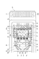
図1は本実施形態に係る発光モジュール1を蓋体7側(以下「一方側」とすることもある)から見た斜視図、図2は発光モジュール1を蓋体7の反対側に位置する放熱面8側(以下「他方側」とすることもある)から見た斜視図、図3(a)は発光モジュール1の平面図、図3(b)は発光モジュール1の側面図、である。図1〜図3に示されるように、本実施形態の発光モジュール1は、上述した筐体2と、フランジ付き円柱状の光結合部3とを有する。筐体2における光結合部3の反対側の側面2aには、RF信号用のリードピンであるRF端子4と、DC信号用のリードピンであるDC端子5とが集中して配置されている。RF端子4及びDC端子5は、筐体2の幅方向にそれぞれ複数並ぶように配置されている。
FIG. 1 is a perspective view of the light emitting module 1 according to the present embodiment as viewed from the lid 7 side (hereinafter sometimes referred to as “one side”), and FIG. 2 is a diagram illustrating the light emitting module 1 positioned on the opposite side of the lid 7. FIG. 3A is a plan view of the light emitting module 1 and FIG. 3B is a side view of the light emitting module 1 as viewed from the
なお、例えばCFP2規格及びCFP4規格では、発光モジュール1が隣接する受光モジュール(ROSA:Receiver Optical Sub-Assembly)と干渉するので、筐体2の他の側面2b(光結合部3が設置される側面2cに接続する両側の側面2b)にRF端子4及びDC端子5を設けることは困難である。従って、RF端子4とDC端子5は、筐体2の長手方向における筐体2の一端のみに配置されている。
For example, in the CFP2 standard and the CFP4 standard, the light emitting module 1 interferes with an adjacent light receiving module (ROSA: Receiver Optical Sub-Assembly), so that the
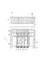
図4及び図5に示されるように、発光モジュール1では、筐体2内に、複数のLD(レーザダイオード、発光素子)11と、LD11を駆動するドライバIC23を含む集積回路等の能動部品と、複数のインダクタ12等の受動部品と、各LD11に対応した個数のPD(Photo Diode:受光素子)14と、各LD11が出射する光を合波する光合波器(Optical Multiplexer)15と、複数のレンズ16等の光学部品と、温調素子(TEC)17と、サーミスタ(温測抵抗体)18等が実装される。
As shown in FIGS. 4 and 5, in the light emitting module 1, an active component such as an integrated circuit including a plurality of LDs (laser diodes, light emitting elements) 11 and a
また、図1〜図3に示されるように、筐体2には、各部品が実装された筐体2の内部を気密封止するために、筐体2の内部を窒素に置換した後に蓋体7がシーム溶接によって接合される。筐体2の内部で光合波器15によって合波された光は、RF端子4及びDC端子5を有する筐体2の側面2aの反対側の側面2cに設けられたサファイア窓を透過し、レンズ及びアイソレータを介して光結合部3に内蔵されたスタブの光ファイバに光結合される。
In addition, as shown in FIGS. 1 to 3, the
光結合部3は、スリーブカバー19とジョイントスリーブ20とを含んでいる。スリーブカバー19内に、外部ファイバの先端に保持されているフェルールを収納するスリーブを有する。スリーブ及びジョイントスリーブ20は、光結合が最適に行われるように3軸調芯された後、YAG溶接によって筐体2に接合される。筐体2には、銅タングステン合金(CuW)等の熱伝導率が高い材料で形成された放熱面8と、RF端子4及びDC端子5を有する側壁セラミック部(多層セラミック層)22と、が設けられている。また、筐体2の内部において、上記の放熱面8上には温調素子17が実装されている(図8参照)。
The
側壁セラミック部22は、複数のセラミック層22aが積層された多層セラミック構造を有しており、各セラミック層22aに配線が形成されている。また、側壁セラミック部22は、各セラミック層22aを貫通して形成されて電気接続を行うために設けられたビアを有している。この配線に筐体2の内部の配線が通されて、その配線は筐体2の外部に設けられたRF端子4及びDC端子5に接続される。
The sidewall
側壁セラミック部22の一方側の面22bには、電源用又は制御信号用のDC端子5が形成されており、他方側の面22cに高速変調信号用のRF端子4が形成されている。放熱面8は、筐体2の内部で生じた熱を効率よく拡散させるため、例えばCuWのような熱伝導率が高い材料で形成されている。また、放熱面8は、発光モジュール1の筐体2が搭載される光トランシーバの金属筐体に対して熱抵抗が小さくなるように、光トランシーバに対して放熱シート等を介して接続される。
A
図4は、本実施形態に係る発光モジュール1の機能ブロック図を示している。図4に示されるように、発光モジュール1では、互いに異なる波長の信号光を出射する4個のLD11が搭載されており、各LD11から出射された光を1つに束ねる光合波器15が設けられている。以下、本実施形態では発光モジュール1が4チャンネルであるものとして説明するが、実際は4チャンネルに限定されない。
FIG. 4 is a functional block diagram of the light emitting module 1 according to the present embodiment. As shown in FIG. 4, the light emitting module 1 includes four
図4及び図5に示されるように、発光モジュール1の内部には温調素子(TEC:Thermo-Electric Controller)17が搭載されており、温調素子17の上に、ドライバIC23と、4個のLD11と、4個のモニタ用のPD14と、光合波器15と、サーミスタ18とが搭載される。LD11、インダクタ12、PD14及びレンズ16は、筐体2の幅方向に並ぶようにそれぞれ4個ずつ設けられている。サーミスタ18は、レンズ16の片側に1個設けられている。なお、サーミスタ18は、DC端子数に制約が無ければ、レンズ16の両側に配置しても良い。
As shown in FIGS. 4 and 5, a temperature control element (TEC: Thermo-Electric Controller) 17 is mounted inside the light emitting module 1, and a
図4に示されるように、RF端子4としては、チャンネル毎に差動の入力を行う端子4aが例えば合計8本設けられる。一方、DC端子5としては、LD11へのバイアス電流の供給を行う4本の端子5aと、温調素子17への電源供給端子である2本の端子5bと、サーミスタ18用の2本の端子5cと、ドライバIC23用の電源端子である1本の端子5dと、ドライバIC23における制御・通信用の端子である2本の端子5eと、複数のグラウンド端子とが設けられる。このように、4チャンネルの発光モジュール1では、1チャンネルで構成される発光モジュールに比べて大幅に端子の数が増大する。従来の発光モジュールでは4個のPD14の出力もDC端子5としていたが、DC端子数の制約により、PD14の出力をドライバIC23でデジタル値に変換した上で、制御・通信用の端子5eを用いて出力している。
As shown in FIG. 4, as the
図5は発光モジュール1の内部における部品配置を示す図であり、図6はドライバIC23付近を拡大させた図であり、図7は部品の実装途中の状態を示す図であり、図8は発光モジュール1の主要部における横断面を示す図である。図8に示されるように、RF端子4はDC端子5に対して反対側の面22cに設けられている。また、側壁セラミック部22におけるRF端子4が設けられるセラミック層22aとDC端子5が設けられるセラミック層22aは、筐体2の長手方向側に突出している。そして、段付き構造となったセラミック層22aにおける一方側の面22bにDC端子5が設けられ他方側の面22cにRF端子4が設けられている。
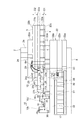
5 is a diagram showing the arrangement of components inside the light emitting module 1, FIG. 6 is an enlarged view of the vicinity of the
図5〜図8に示されるように、DC端子5からの配線(側壁セラミック部22の面22b上の配線)は、その高さを維持しつつ筐体2内に導かれ、筐体2内のDC端子24と接続している。温調素子17用の配線17aは、ビアを介して側壁セラミック部22の下から2段目まで引き回された設計となっている。DC端子24は、ワイヤボンディングによって、インダクタ12を搭載するインダクタキャリア25上の電極パッド25aと、キャパシタ26上の電極パッド26aと、キャパシタ26を搭載する配線基板27上の電極パッド27aに接続される。
As shown in FIGS. 5 to 8, the wiring from the DC terminal 5 (wiring on the
筐体2の内部におけるDC端子24の高さは、接続先である、インダクタキャリア25上の電極パッド25a、キャパシタ26上の電極パッド26a、及び配線基板27上の電極パッド27aのいずれよりも高くなっている。DC端子24から引き出されたボンディングワイヤB4のDC端子24に対する角度は鋭角となっている。また、各ボンディングワイヤB4は、インダクタキャリア25の電極パッド25a、キャパシタ26の電極パッド26a、及び配線基板27の電極パッド27aのそれぞれに対して垂直に伸びている。
The height of the
RF端子4からの配線(側壁セラミック部22の面22c上の配線)は、高速信号を伝搬する配線である。この配線は、その高さを維持しつつ筐体2内に導かれ、筐体2内のRF端子29と接続している。このように、高速信号を伝搬する配線を、ビアなどを介さず同一平面上に設計することで、特性インピーダンスの不整合が生じ難く、良好な高周波特性を実現することができる。このRF端子29は、ワイヤボンディングによって、ドライバIC23上の電極パッド23aに直接接続される。
The wiring from the RF terminal 4 (wiring on the
図8に示されるように、筐体2の内部におけるRF端子29の高さは、ドライバIC23上の電極パッド23aの高さと比較して、実質的に等しいか、又はボールボンディングを行うために僅かに低くなっている。RF端子29及び電極パッド23aでは、まず、電極パッド23aに対し第1のボンディングを行い、ボンディングワイヤB1を引き出しつつ、RF端子29上にボンディングヘッドを移動させて、RF端子29に第2のボンディングを行う。上述したようにRF端子29の高さがドライバIC23の電極パッド23aよりも僅かに低い場合、上記のボンディングワイヤB1を引き出す動作をスムーズに行うことが可能となる。
As shown in FIG. 8, the height of the
ドライバIC23上の電極パッド23aから引き出されたボンディングワイヤB1は、斜め上方に伸びている。また、側壁セラミック部22上のRF端子29に接続し、その接触角度は、電極パッド23aに対する角度よりも僅かに大きい。このように、RF端子29と電極パッド23aとを接続するボンディングワイヤB1は、ドライバIC23の電極パッド23aから若干斜め上方に伸びると共にRF端子29からも斜め上方に伸びている。RF端子29の高さをドライバIC23の電極パッド23aよりも僅かに低くすることによって上記のようにボンディングワイヤB1を接続することが可能となる。
The bonding wire B1 drawn from the
また、ドライバIC23の信号出力用の電極パッド23bは、LD11の電極パッド11aとワイヤボンディングによって接続され、LD11における電極パッド11aの高さは、ドライバIC23における電極パッド23bの高さと比較して僅かに低くなっている。よって、ドライバIC23とLD11とを接続するボンディングワイヤB2を、プル強度(電極パッド11aと電極パッド23bにボンディングされたボンディングワイヤB2における接着強度の指標)を確保しつつ、ボンディングワイヤB2の長さを最短にすることが可能となる。
The
図6〜図8に示されるように、筐体2の内部では、放熱面8の内面に温調素子17が搭載されている。温調素子17上にはキャリア32が搭載されており、キャリア32上にはICキャリア30、LDサブマウント31及びサーミスタ用基板36が搭載されている。ICキャリア30上にはドライバIC23及び配線基板27が搭載されており、LDサブマウント31上にはLD11が搭載されている。ドライバIC23上にはスペーサ28が搭載されており、スペーサ28上にはインダクタキャリア25が搭載されており、更にインダクタキャリア25上にはインダクタ12が搭載されている。
As shown in FIGS. 6 to 8, the
LDサブマウント31は、ドライバIC23における側壁セラミック部22の反対側に配置されており、キャリア32上で筐体2の幅方向に並ぶように2個設けられている。各LDサブマウント31上には2個のLD11が筐体2の幅方向に並ぶように搭載されている。また、配線基板27はドライバIC23の両脇に2個配置されており、配線基板27における側壁セラミック部22の反対側にサーミスタ用基板36が1個配置されている。
Two LD submounts 31 are arranged on the opposite side of the side wall
また、例えば、スペーサ28は厚さが350μmのSi製もしくはAlN製、インダクタキャリア25は厚さが350μmのSiO2製、ドライバIC23を搭載するICキャリア30は厚さが300μmのAlN製、LD11を搭載するLDサブマウント31とレンズ16等の部品を搭載するキャリア32は厚さが450μmのAlN製、である。スペーサ28はドライバIC23の上方に配置されるが、ドライバIC23の上面に設けられた集積回路の特性に悪影響を及ぼさないよう、ドライバIC23の線膨張係数と近い材料であることが好ましい。インダクタキャリア25にはインダクタ12を実装するための電極パターンが配置されるが、この電極パターンの面積とインダクタキャリア25の材料に依存する比誘電率とによって生じる寄生容量が発生する。寄生容量が大きいと高周波特性に悪影響を与えるため、インダクタキャリア25の材料は比誘電率が低いSiO2であることが好ましい。一方、ICキャリア30及びLDサブマウント31は、ドライバIC23及びLD11から生じる熱を効率よく拡散するため、熱伝導率の高い材料が好ましい。キャリア32も同様に熱伝導率が高い材料を用い、ドライバIC23及びLD11から生じた熱を拡散させて、温調素子17に対して温度勾配が少なくすることが好ましい。
Further, for example, the
また、図5に示されるように、LD11は4チャンネル分が実装されており、各LD11が出射した光は、1個又は複数個のレンズ16を介して光合波器15に入射される。そして、光合波器15によって4チャンネルの光信号が1本に束ねられ合波されてから出射される。モニタ用のPD14は、光路における光合波器15の手前側に設置されており、各PD14は、各LD11から出射された光のパワーをモニタするために用いられる。光合波器15から出射された光は、1個又は複数個のレンズ33を介して光結合部3に内蔵されるスタブの光ファイバで結合され、光結合部3のスリーブカバー19に光コネクタを挿入することによって発光モジュール1からの光の伝送が可能となる。なお、LD11から上記のスタブの間には、光ファイバの端面等からの反射戻り光を抑制させるためのアイソレータを配置してもよい。
Further, as shown in FIG. 5, four channels of the
ところで、ドライバIC23上に設けられた電極パッド23aに対しては図5〜図8の紙面右側から高速変調信号の入力がなされ、ドライバIC23上に設けられた電極パッド23bからは図5〜図8の紙面左側に向かって高速変調信号の出力(LD11への信号の入力)がなされる。図5〜図7の紙面上側及び紙面下側には、電源用、PD14用、及び制御・通信用の端子等が配置される。
By the way, a high-speed modulation signal is input to the
発光モジュール1において、RF信号は、各チャネルの差動信号として入力される。側壁セラミック部22におけるRF信号の配線は、G、Sig+、Sig−、Gの4本1組の配置で設けられており、4本1組のチャネルが4個含まれている。一方、ドライバIC23上の電極パッド23aについてはSig+とSig−との間にGNDパッドが形成されている。このドライバIC23のGNDパッドは、ワイヤボンディングではなくドライバIC23上で結線されることによって接続が実現されている。また、側壁セラミック部22におけるRF信号の配線は、G、Sig+、G、Sig−、Gの5本1組の配置で設けても良い。その場合、ドライバIC23の電極パッド23aに対してそのまま結線することができる。
In the light emitting module 1, the RF signal is input as a differential signal of each channel. The wiring of the RF signal in the side wall
図6及び図7に示されるように、ドライバIC23の電極パッド23aからドライバIC23の一辺に沿うように形成されたLDドライバ回路23dに信号が供給される。なお、ドライバIC23におけるチップ内の他の箇所にはデジタル回路等の制御部が形成されている。上記のLDドライバ回路23dで増幅された駆動信号は、ドライバIC23の左辺に形成された出力用の電極パッド23bからボンディングワイヤB2を介してLD11に供給される。このようにドライバIC23からは、各LD11に直接ボンディングワイヤB2が伸ばされている。
As shown in FIGS. 6 and 7, a signal is supplied from the
LD11は、n−type基板上に活性層を形成した端面発光型のLDである。ここで、n基板を採用するLDはエピダウンで(基板側が上側、活性層及び他のエピ成長層が下側となるように)実装され、n基板側を信号用、p層側をGNDもしくはVcc用として用いるのが通常である。しかしながら、LD11は、基板のn電極(アノード)をチップ内部でビアホール等によりp層側に持ち上げることによって、n基板側を実装する形態であっても、チップ表面にn電極及びp電極(カソード)の両方が設けられている。これは、LD11をいわゆるシャント駆動する所以である。シャント駆動ではp側に駆動信号を入力しn側をGNDもしくはVssとして用いるからである。ドライバIC23から引き出された2本のボンディングワイヤB2のうち一方はLD11のアノードに他方はLD11のカソードにそれぞれ接続されるが、図8に示されるように、上記2本のボンディングワイヤB2は共にLD11のチップ表面に形成された電極パッド11aに接続される。
The
また、図10及び図11に示されるように、LD11のアノードに接続されるLDサブマウント31上の電極パッド(中継パッド)31aには、インダクタキャリア25上に実装されたインダクタ12からの接続がなされる。インダクタキャリア25上には、各チャンネルに対応した4本の配線25bが設けられており、その途中にチップインダクタであるインダクタ12が実装される。また、上記のように、LDサブマウント31が電極パッド31aを備えているので、インダクタ12から供給されるバイアス電流は、上記の電極パッド31aを介してLD11に供給される。
As shown in FIGS. 10 and 11, the electrode pad (relay pad) 31 a on the LD submount 31 connected to the anode of the
また、LD11の駆動はシャントドライブと称される形式で行われ、LD11に対して並列にSW−Tr(スイッチングトランジスタ)が接続されている。このSW−TrがOn/Offされることにより、LD11に流れる電流がSW−Trに分流される。このように分流される構成がシャント(分流)形式と称される。LD11とSW−Trとの並列回路には、インダクタ12を介してバイアス電流が供給される。
The
インダクタキャリア25上に実装されるインダクタ12は、上述したバイアス電流をLD11に供給するためのインダクタである。また、上述したSW−Trのスイッチング特性がバイアス電流源に影響しないように大きなインダクタンスを必要とするためインダクタ12のサイズが大きくなるので、発光モジュール1では如何にこのインダクタ12を実装するかが重要となる。そこで、本実施形態では、ドライバIC23の上方に空間を設けており、ドライバIC23の上部空間に余裕を持たせている。
The
また、本実施形態では、上記のようにシャントドライブ回路を用いることによって消費電力を抑えることが可能となっているので、ドライバIC23の放熱対策としてドライバIC23の上部空間等のレイアウトを考慮する必要性は小さい。また、温調素子17の上部に位置するキャリア32がLDサブマウント31とICキャリア30とを搭載し、ドライバIC23はICキャリア30に搭載されている。よって、ドライバIC23は、ICキャリア30及びキャリア32を介して温調素子17によって冷却されるので、ドライバIC23に対する適切な温度環境が実現されている。
In this embodiment, since the power consumption can be suppressed by using the shunt drive circuit as described above, it is necessary to consider the layout of the upper space of the
また、ドライバIC23の上方でインダクタ12が実装されており、インダクタ12からLDサブマウント31上の電極パッド31aまでのボンディングワイヤB3の長さはドライバIC23の入出力に係るボンディングワイヤB2の長さよりも長い。このようにインダクタ12からLDサブマウント31上の電極パッド31aまでのボンディングワイヤB3の長さは筐体2の部品配置によって長くなっているが、このことによって動作上の問題は発生しない。そもそも、上記のボンディングワイヤB3は、インダクタ12に向けての配線でありインダクタンスが必要とされる箇所の配線である。このボンディングワイヤB3としては、寄生抵抗を増加させない程度の細径のものを採用することが好ましい。なお、ボンディングワイヤを細径にすればするほど、その寄生インダクタンスは大きくなる。
The
図11及び図12に示されるように、ドライバIC23の周辺には、電源のパスコンデンサ等として用いられるキャパシタ26、及びLD11に供給するバイアス電流の配線上に設置されるインダクタ12等の受動部品が配置される。また、4チャンネルのモニタ用PD14の配線L1、サーミスタ18の配線L2、及び制御・通信用の配線等は、筐体2の内部の実装部品を介して筐体2のDC端子24に電気的に接続されている。なお、各部品からDC端子24に直線的にワイヤリングで接続できないため、コンデンサ用の実装面を有し内層に配線を引き回した構造を有する配線基板27を用いて電気接続が行われる。この配線基板27を用いることによって、各ワイヤが交差することを回避した電気配線を実現させることができる。
As shown in FIG. 11 and FIG. 12, passive components such as a
また、筐体2の内部における放熱面8上には温調素子17が実装されており、温調素子17の上面に、筐体2の内部における全ての部品を搭載するための実装基板であるキャリア32が配置される。キャリア32の側壁セラミック部22側には、ドライバIC23を実装するためのICキャリア30が搭載される。ICキャリア30上には、ドライバIC23及び配線基板27が配置される。また、ドライバIC23上方の上部空間を有効利用するため、ドライバIC23の上方にインダクタ12が配置される。
Further, the
図8に示されるように、ドライバIC23上でワイヤリングの干渉等が生じないようにするために、ドライバIC23の上方には、ドライバIC23の上面に位置するスペーサ28を介してインダクタキャリア(インダクタ実装基板)25が配置されている。インダクタキャリア25上にはインダクタ12が4チャンネル分実装されている。また、筐体2内では、筐体2の内部のDC端子24からインダクタキャリア25上の入力配線にボンディングワイヤB4によってワイヤリングされ、インダクタ12を介してボンディングワイヤB3を用いてLD11にワイヤリングを行うことによって電気的な接続が実現される。
As shown in FIG. 8, in order to prevent wiring interference or the like on the
インダクタ12からLD11の電極パッド11aまでの配線には、ドライバIC23から出力される高速変調信号の一部が流れ込むため、インダクタキャリア25に設けられたインダクタ実装用の電極パッド25aが寄生容量として高周波信号のリークに影響するという問題がある。そこで、インダクタキャリア25における電極パッド25aのサイズを実装可能な範囲で小さく設計する必要がある。また、電極パッド25aが配置される基材の比誘電率が小さい方が寄生容量を抑制することができるため、電極パッド25aの材料としては、セラミックよりも比誘電率が小さい石英又はテフロン(登録商標)等の材料を用いることが好ましい。
Since a part of the high speed modulation signal output from the
図12に示されるように、筐体2に含まれる側壁セラミック部22について、筐体2の内部のRF端子29は、筐体2の外部のRF端子4が配置される面22cに対向する面22dに形成されている。すなわち、筐体2の外部におけるRF端子4を形成するセラミック層22aと、筐体2の内部におけるRF端子29を形成するセラミック層22aとは異なっており、かつRF端子4を形成する面22cとRF端子29を形成する面22dとが対向している。
As shown in FIG. 12, with respect to the side wall
RF端子29から延びるRF配線としては、マイクロストリップライン又はコプレナーラインといった伝送線路を用いて特性インピーダンスが単相の場合は50Ω、差動の場合は100Ωとなるように設計するのが好ましい。また、筐体2の外部のRF端子4と筐体2の内部のRF端子29のように、伝送線路を表裏反転した同一面上に形成することで、異なる面上に形成した場合には必要となるビアを用いた配線が不要となり、ビアの部分で生じる特性インピーダンスの乱れを無くすことができる。
The RF wiring extending from the
ところで、仮に図9に示されるドライバIC23のDC端子23eが図9の紙面における上下方向に沿って配置されているとすると、DC端子23eを筐体2のDC端子24に直接接続する際にクロスワイヤ等の懸念が生じるので設計が困難になる。また、CFP規格等、発光モジュールのサイズにおける制約が小さい場合には筐体2の幅(図9の紙面における上下方向の長さ)を長くして側壁セラミック部22のDC端子24と平行となるよう配置することが可能ではある。しかしながら、筐体2の幅を短くしたCFP2規格又はCFP4規格で搭載可能な発光モジュール1を設計する場合、筐体2の幅に制約があるので、ドライバIC23のDC端子23eと側壁セラミック部22のDC端子24とを平行に配置することが困難となる。
If the DC terminal 23e of the
そこで、本実施形態では、ドライバIC23のDC端子23eに対して平行な端子27cを有する配線基板27を用いて、DC端子23eとDC端子24とが配線基板27を介して接続される。このように、複数の端子27cを有する配線基板27を用いて接続を行うことによって、ドライバIC23のDC端子23eと筐体2のDC端子24とを無理なく接続できるようにしている。
Therefore, in the present embodiment, the DC terminal 23 e and the
配線基板27における一方側の表層27bはキャパシタ26等の部品を実装可能とするため幅の大きいグラウンド面となっており、表層27bの内部側に配線が設けられている。よって、ドライバIC23のDC端子23eを引き回し筐体2のDC端子24に対して無理が生じないように配線することを可能にしている。また、この配線基板27を用いることによって、ドライバIC23の表面23c側を経由するワイヤ等を無くすことができるため、ドライバIC23の表面23cにインダクタ12等の部品を実装することが可能となっている。
The
また、本実施形態では、スペーサ28がドライバIC23の表面23cに実装されると共に、インダクタキャリア25がスペーサ28の上面に実装される。このように、配線基板27によって必要とされるボンディングワイヤの長さを短くし、ドライバIC23上にも部品を搭載可能とした設計を用いることによって、必要な能動部品及び受動部品を限られたスペースで高密度に搭載可能としている。
In the present embodiment, the
また、発光モジュール1では、図5に示されるように、各LD11からの信号光がレンズ16を構成する第1レンズ16a及び第2レンズ16bを介して光マルチプレクサである光合波器15に入力される。第2レンズ16bと光合波器15との間には、ビームスプリッタ35(図12参照)が設けられ、このビームスプリッタ35上にPD14がマウントされる。ビームスプリッタ35によってLD11の出射光の一部が分岐されて各PD14に入力され、各PD14の電気的出力(光電流)は、第1及び第2のレンズ16a,16bの両脇に配置されたサーミスタ用基板36を介して配線基板27に入力され、配線基板27からドライバIC23の内部における制御回路(APC回路)に入力される。
Further, in the light emitting module 1, as shown in FIG. 5, the signal light from each
ここで、第1レンズ16aを集光レンズとし、第2レンズ16bをコリメートレンズ又は集光レンズとすることができる。そして、第1レンズ16aの一方の焦点にLD11の出射端面を配置し、第1レンズ16aの他方の焦点と第2レンズ16bの一方の焦点とを実質的に一致させる光学系を採用することができる。この光学系を採用することによって、例えば光合波器15としてAWG(Arrayed Wave Guide)を用いた場合には、第2レンズ16bを集光レンズとすることでAWGの導波路にLD11からの光を集光することが容易となる。例えば光合波器15としてWDMフィルタを組み合わせた系を採用する場合には、第2レンズ16bをコリメートレンズとすることで筐体2の出口に設けられたレンズ33における結合効率を容易に向上させることができる。なお、レンズ33からの出力光は、光結合系内の結合ファイバ端面に集光される。
Here, the
本実施形態では、インダクタキャリア25とドライバIC23との間に位置するスペーサ28を用いてドライバIC23の上方にインダクタ12を配置しているので、筐体2の内部における各ワイヤを短くすると共に、筐体2の内部の限られたスペースにおける効率的な部品配置が実現されている。
In the present embodiment, since the
図8に示されるように、側壁セラミック部22の他方側の面22cとドライバIC23の上側(一方側)の表面23cとの距離D1は、側壁セラミック部22の一方側の22bとインダクタキャリア25におけるインダクタ12を搭載する面との距離D2よりも短い。すなわち、側壁セラミック部22の面22cとドライバIC23の表面23cとの段差は、側壁セラミック部22の面22bとインダクタキャリア25のインダクタ12を搭載する面との段差よりも小さくなっている。よって、ドライバIC23とRF端子29とを接続するRF信号用のボンディングワイヤB1を、インダクタキャリア25とDC端子24とを接続するDC信号用のボンディングワイヤB4よりも短くすることができる。
As shown in FIG. 8, the distance D1 between the
図11及び図12に示されるように、ICキャリア30は配線基板27を搭載しており、配線基板27はICキャリア30上でドライバIC23に隣接して配置されている。また、配線基板27は、ドライバIC23の両脇に2個設けられており、ドライバIC23を筐体2の幅方向側から挟み込むように設けられている。よって、筐体2内におけるRF信号用の配線は筐体2の長手方向に沿うように直線的に接続されると共に、筐体2内におけるDC信号用の配線は両側から上記RF信号用の配線を回り込むように各部品に接続される。従って、配線の交差を防止しつつRF信号用の配線を短くさせた効率の良い配線が実現されている。
As shown in FIGS. 11 and 12, the
以上、本発明に係る好適な実施形態について図示し説明してきたが、本発明は上述した実施形態に限定されるものではない。すなわち、特許請求の範囲に記載された本発明の要旨の範囲内において、種々の変形及び変更が可能であることは、当業者によって容易に認識される。 As mentioned above, although preferred embodiment which concerns on this invention has been shown and described, this invention is not limited to embodiment mentioned above. That is, it is easily recognized by those skilled in the art that various modifications and changes can be made within the scope of the gist of the present invention described in the claims.
例えば、上記実施形態では、筐体2の内部におけるRF端子29の高さがドライバIC23上の電極パッド23aの高さよりも僅かに低くなっている例について説明したが、RF端子29の高さを電極パッド23aの高さより高くすることも可能である。ただし、ドライバIC23の電極パッド23aは他の電極パッドより小さく先にボンディングすることが好ましいので、RF端子29の高さが電極パッド23aの高さより低い方がボンディングのし易さの点では有利である。
For example, in the above embodiment, the example in which the height of the
1…発光モジュール、2…筐体、3…光結合部、4…RF端子、5…DC端子、7…蓋体、8…放熱面、11…LD、12…インダクタ、14…PD、15…光合波器、16…レンズ、16a…第1レンズ、16b…第2レンズ、17…温調素子、18…サーミスタ、19…スリーブカバー、20…ジョイントスリーブ、22…側壁セラミック部(多層セラミック層)、22a…セラミック層、23…ドライバIC、23a,23b…電極パッド、24…DC端子、25…インダクタキャリア、26…キャパシタ、27…配線基板、28…スペーサ、29…RF端子、30…ICキャリア、31…LDサブマウント、32…キャリア、33…レンズ、35…ビームスプリッタ、36…サーミスタ用基板、B1,B2,B3,B4…ボンディングワイヤ、D1,D2…距離、L1,L2…配線。
DESCRIPTION OF SYMBOLS 1 ... Light emitting module, 2 ... Housing | casing, 3 ... Optical coupling part, 4 ... RF terminal, 5 ... DC terminal, 7 ... Cover body, 8 ... Radiation surface, 11 ... LD, 12 ... Inductor, 14 ... PD, 15 ... Optical multiplexer, 16 ... lens, 16a ... first lens, 16b ... second lens, 17 ... temperature control element, 18 ... thermistor, 19 ... sleeve cover, 20 ... joint sleeve, 22 ... side wall ceramic part (multilayer ceramic layer) 22a ... ceramic layer, 23 ... driver IC, 23a, 23b ... electrode pad, 24 ... DC terminal, 25 ... inductor carrier, 26 ... capacitor, 27 ... wiring board, 28 ... spacer, 29 ... RF terminal, 30 ...
Claims (9)
前記複数のレーザダイオードを駆動するドライバICと、
前記複数のレーザダイオードのそれぞれにバイアス電流を供給する複数のインダクタと、
前記複数のインダクタを搭載するインダクタキャリアと、
前記インダクタキャリアと前記ドライバICとの間に位置するスペーサと、
を備え、
前記スペーサは前記ドライバICに搭載されており、前記インダクタキャリアは前記スペーサに搭載されている、発光モジュール。 A plurality of laser diodes emitting signal lights of different wavelengths;
A driver IC for driving the plurality of laser diodes;
A plurality of inductors for supplying a bias current to each of the plurality of laser diodes;
An inductor carrier carrying the plurality of inductors;
A spacer positioned between the inductor carrier and the driver IC;
Equipped with a,
The light emitting module, wherein the spacer is mounted on the driver IC, and the inductor carrier is mounted on the spacer .
前記多層セラミック層の一方側の面に設けられたDC端子と、
前記多層セラミック層における前記一方側の面と反対側の他方側の面に設けられたRF端子と、
を備え、
前記多層セラミック層の前記他方側の面と前記ドライバICの前記一方側の面との段差は、前記多層セラミック層の前記一方側の面と前記インダクタキャリアにおける前記インダクタを搭載する面との段差よりも小さい、請求項1に記載の発光モジュール。 A housing including a multilayer ceramic layer;
DC terminals provided on one side of the multilayer ceramic layer;
An RF terminal provided on the other side of the multilayer ceramic layer opposite to the one side;
With
The level difference between the other side surface of the multilayer ceramic layer and the one side surface of the driver IC is greater than the level difference between the one side surface of the multilayer ceramic layer and the surface on which the inductor is mounted in the inductor carrier. The light emitting module according to claim 1, which is also smaller.
前記複数のレーザダイオードを搭載するLDサブマウントと、
前記LDサブマウントと前記ICキャリアとを搭載する実装基板と、
を備え、
前記実装基板は、温調素子上に搭載されている、請求項1〜4のいずれか一項に記載の発光モジュール。 An IC carrier on which the driver IC is mounted;
An LD submount on which the plurality of laser diodes are mounted;
A mounting substrate on which the LD submount and the IC carrier are mounted;
With
The light emitting module according to any one of claims 1 to 4, wherein the mounting substrate is mounted on a temperature control element.
前記配線基板は、前記ICキャリア上で前記ドライバICに隣接して配置されている、
請求項5に記載の発光モジュール。 The IC carrier further includes a wiring board,
The wiring board is disposed adjacent to the driver IC on the IC carrier.
The light emitting module according to claim 5.
前記インダクタから供給される前記バイアス電流は、前記中継パッドを介して前記レーザダイオードに供給される、請求項5又は6に記載の発光モジュール。 The LD submount includes a relay pad,
The light emitting module according to claim 5 or 6, wherein the bias current supplied from the inductor is supplied to the laser diode via the relay pad.
前記スイッチングトランジスタは、前記レーザダイオードに対して並列に接続されている、請求項1〜8のいずれか一項に記載の発光モジュール。 A switching transistor for shunting the bias current supplied from the inductor;
The light emitting module according to claim 1, wherein the switching transistor is connected in parallel to the laser diode.
Priority Applications (3)
| Application Number | Priority Date | Filing Date | Title |
|---|---|---|---|
| JP2013232092A JP6232950B2 (en) | 2013-11-08 | 2013-11-08 | Light emitting module |
| US14/534,956 US9385830B2 (en) | 2013-11-08 | 2014-11-06 | Transmitter module outputting wavelength multiplexed light |
| CN201410638499.9A CN104638509B (en) | 2013-11-08 | 2014-11-06 | The transmitter module of output wavelength multiplexed optical |
Applications Claiming Priority (1)
| Application Number | Priority Date | Filing Date | Title |
|---|---|---|---|
| JP2013232092A JP6232950B2 (en) | 2013-11-08 | 2013-11-08 | Light emitting module |
Publications (2)
| Publication Number | Publication Date |
|---|---|
| JP2015095471A JP2015095471A (en) | 2015-05-18 |
| JP6232950B2 true JP6232950B2 (en) | 2017-11-22 |
Family
ID=53043898
Family Applications (1)
| Application Number | Title | Priority Date | Filing Date |
|---|---|---|---|
| JP2013232092A Active JP6232950B2 (en) | 2013-11-08 | 2013-11-08 | Light emitting module |
Country Status (3)
| Country | Link |
|---|---|
| US (1) | US9385830B2 (en) |
| JP (1) | JP6232950B2 (en) |
| CN (1) | CN104638509B (en) |
Families Citing this family (7)
| Publication number | Priority date | Publication date | Assignee | Title |
|---|---|---|---|---|
| JP6555106B2 (en) * | 2015-12-02 | 2019-08-07 | 三菱電機株式会社 | Optical module |
| JP2018074057A (en) * | 2016-11-01 | 2018-05-10 | 住友電工デバイス・イノベーション株式会社 | Semiconductor laser carrier assembly, optical semiconductor device, and manufacturing method of optical semiconductor device |
| CN106998230B (en) * | 2017-03-07 | 2019-07-09 | 武汉光迅科技股份有限公司 | Dual rate DML device, module and the signal calibration method of built-in signal calibration circuit |
| JP2019029394A (en) | 2017-07-26 | 2019-02-21 | 住友電気工業株式会社 | Carrier mounting structure |
| JP6986453B2 (en) * | 2018-01-12 | 2021-12-22 | ローム株式会社 | Semiconductor laser device |
| CN109586797B (en) * | 2018-11-16 | 2020-05-12 | 武汉电信器件有限公司 | Laser emitting assembly and corresponding optical module |
| CN114334865B (en) * | 2022-03-07 | 2022-07-26 | 成都雷电微力科技股份有限公司 | Three-dimensional high-power TR that piles up seals dress subassembly |
Family Cites Families (13)
| Publication number | Priority date | Publication date | Assignee | Title |
|---|---|---|---|---|
| US6590916B2 (en) * | 2001-02-08 | 2003-07-08 | Quantum Devices, Inc. | Method for fabricating a wave division laser array multiplexer |
| WO2003096759A1 (en) * | 2001-03-30 | 2003-11-20 | Santur Corporation | High speed modulation of arrayed lasers |
| JP2003014994A (en) * | 2001-07-04 | 2003-01-15 | Hitachi Ltd | Multi-channel optical element mounting substrate and optical communication module |
| KR100477990B1 (en) * | 2002-09-10 | 2005-03-23 | 삼성에스디아이 주식회사 | Plasma display panel and driving apparatus and method thereof |
| JP2004179204A (en) * | 2002-11-25 | 2004-06-24 | Mitsubishi Electric Corp | Optical element module |
| US20060140233A1 (en) * | 2004-12-28 | 2006-06-29 | Jesse Chin | Laser driver with integrated bond options for selectable currents |
| JP5071248B2 (en) * | 2008-06-03 | 2012-11-14 | 住友電気工業株式会社 | Laser diode drive circuit |
| WO2010088631A2 (en) | 2009-01-30 | 2010-08-05 | Kaiam Corp. | Micromechanically aligned optical assembly |
| JP5361817B2 (en) * | 2010-07-08 | 2013-12-04 | 三菱電機株式会社 | Optical module |
| JP5859219B2 (en) * | 2011-04-22 | 2016-02-10 | 日本オクラロ株式会社 | Differential transmission line and communication device |
| US8380073B2 (en) * | 2011-05-24 | 2013-02-19 | Sumitomo Electric Industries, Ltd. | Optical transceiver implemented with tunable LD |
| JP2013153136A (en) * | 2011-12-27 | 2013-08-08 | Sumitomo Electric Ind Ltd | Light-emitting module and optical transceiver |
| JP2013140292A (en) * | 2012-01-06 | 2013-07-18 | Sumitomo Electric Ind Ltd | Optical receiver module |
-
2013
- 2013-11-08 JP JP2013232092A patent/JP6232950B2/en active Active
-
2014
- 2014-11-06 US US14/534,956 patent/US9385830B2/en active Active
- 2014-11-06 CN CN201410638499.9A patent/CN104638509B/en not_active Expired - Fee Related
Also Published As
| Publication number | Publication date |
|---|---|
| CN104638509B (en) | 2019-03-22 |
| US20150132001A1 (en) | 2015-05-14 |
| JP2015095471A (en) | 2015-05-18 |
| US9385830B2 (en) | 2016-07-05 |
| CN104638509A (en) | 2015-05-20 |
Similar Documents
| Publication | Publication Date | Title |
|---|---|---|
| JP6232950B2 (en) | Light emitting module | |
| JP4670384B2 (en) | Method for manufacturing optical transmission assembly | |
| JP6511776B2 (en) | Light emitting module | |
| JP6064530B2 (en) | Light emitting module and optical transceiver | |
| US20120328229A1 (en) | Optical Module | |
| JP2013153136A (en) | Light-emitting module and optical transceiver | |
| JP2019036584A (en) | Optical module | |
| JP7338713B2 (en) | Carrier mounting structure | |
| JP4951971B2 (en) | Photoelectric composite module | |
| JP6984801B1 (en) | Semiconductor laser light source device | |
| JP2007207803A (en) | Optical transmitting module | |
| JP4718135B2 (en) | Optical module | |
| CN111293582A (en) | Optical signal transmitting device | |
| JP6376377B2 (en) | Optical device | |
| JP2006237436A (en) | Light emitting element module | |
| JP3888525B2 (en) | Optical communication module | |
| JP2009260095A (en) | Optical module | |
| JP5649422B2 (en) | Optical device manufacturing method | |
| JP6228560B2 (en) | High frequency transmission line and optical circuit | |
| JP2013110138A (en) | Light emitting module | |
| JP6260167B2 (en) | Photoelectric fusion module | |
| JP2003014990A (en) | Optical communication module | |
| CN211456208U (en) | Optical signal transmitting device | |
| US20210211199A1 (en) | Substrate with stepped profile for mounting transmitter optical subassemblies and an optical transmitter or transceiver implementing same | |
| JP2012023325A (en) | Light emitting module |
Legal Events
| Date | Code | Title | Description |
|---|---|---|---|
| A621 | Written request for application examination |
Free format text: JAPANESE INTERMEDIATE CODE: A621 Effective date: 20161104 |
|
| A977 | Report on retrieval |
Free format text: JAPANESE INTERMEDIATE CODE: A971007 Effective date: 20170719 |
|
| A131 | Notification of reasons for refusal |
Free format text: JAPANESE INTERMEDIATE CODE: A131 Effective date: 20170725 |
|
| A521 | Request for written amendment filed |
Free format text: JAPANESE INTERMEDIATE CODE: A523 Effective date: 20170906 |
|
| TRDD | Decision of grant or rejection written | ||
| A01 | Written decision to grant a patent or to grant a registration (utility model) |
Free format text: JAPANESE INTERMEDIATE CODE: A01 Effective date: 20170926 |
|
| A61 | First payment of annual fees (during grant procedure) |
Free format text: JAPANESE INTERMEDIATE CODE: A61 Effective date: 20171009 |
|
| R150 | Certificate of patent or registration of utility model |
Ref document number: 6232950 Country of ref document: JP Free format text: JAPANESE INTERMEDIATE CODE: R150 |
|
| R250 | Receipt of annual fees |
Free format text: JAPANESE INTERMEDIATE CODE: R250 |
|
| R250 | Receipt of annual fees |
Free format text: JAPANESE INTERMEDIATE CODE: R250 |
|
| R250 | Receipt of annual fees |
Free format text: JAPANESE INTERMEDIATE CODE: R250 |
|
| R250 | Receipt of annual fees |
Free format text: JAPANESE INTERMEDIATE CODE: R250 |