EP1398723B1 - Kontaktiervorrichtung für eine Chipkarte, insbesondere für eine SIM-Karte - Google Patents
Kontaktiervorrichtung für eine Chipkarte, insbesondere für eine SIM-Karte Download PDFInfo
- Publication number
- EP1398723B1 EP1398723B1 EP03015425A EP03015425A EP1398723B1 EP 1398723 B1 EP1398723 B1 EP 1398723B1 EP 03015425 A EP03015425 A EP 03015425A EP 03015425 A EP03015425 A EP 03015425A EP 1398723 B1 EP1398723 B1 EP 1398723B1
- Authority
- EP
- European Patent Office
- Prior art keywords
- contact
- cover
- contacting device
- lid
- carrier
- Prior art date
- Legal status (The legal status is an assumption and is not a legal conclusion. Google has not performed a legal analysis and makes no representation as to the accuracy of the status listed.)
- Expired - Lifetime
Links
Images


Classifications
-
- G—PHYSICS
- G06—COMPUTING OR CALCULATING; COUNTING
- G06K—GRAPHICAL DATA READING; PRESENTATION OF DATA; RECORD CARRIERS; HANDLING RECORD CARRIERS
- G06K7/00—Methods or arrangements for sensing record carriers, e.g. for reading patterns
- G06K7/0013—Methods or arrangements for sensing record carriers, e.g. for reading patterns by galvanic contacts, e.g. card connectors for ISO-7816 compliant smart cards or memory cards, e.g. SD card readers
- G06K7/0021—Methods or arrangements for sensing record carriers, e.g. for reading patterns by galvanic contacts, e.g. card connectors for ISO-7816 compliant smart cards or memory cards, e.g. SD card readers for reading/sensing record carriers having surface contacts
-
- G—PHYSICS
- G06—COMPUTING OR CALCULATING; COUNTING
- G06K—GRAPHICAL DATA READING; PRESENTATION OF DATA; RECORD CARRIERS; HANDLING RECORD CARRIERS
- G06K13/00—Conveying record carriers from one station to another, e.g. from stack to punching mechanism
- G06K13/02—Conveying record carriers from one station to another, e.g. from stack to punching mechanism the record carrier having longitudinal dimension comparable with transverse dimension, e.g. punched card
- G06K13/08—Feeding or discharging cards
-
- G—PHYSICS
- G06—COMPUTING OR CALCULATING; COUNTING
- G06K—GRAPHICAL DATA READING; PRESENTATION OF DATA; RECORD CARRIERS; HANDLING RECORD CARRIERS
- G06K13/00—Conveying record carriers from one station to another, e.g. from stack to punching mechanism
- G06K13/02—Conveying record carriers from one station to another, e.g. from stack to punching mechanism the record carrier having longitudinal dimension comparable with transverse dimension, e.g. punched card
- G06K13/08—Feeding or discharging cards
- G06K13/085—Feeding or discharging cards using an arrangement for locking the inserted card
- G06K13/0862—Feeding or discharging cards using an arrangement for locking the inserted card the locking arrangement being of the rotate-slide and lock type, such as, e.g. common in mobile phones
-
- G—PHYSICS
- G06—COMPUTING OR CALCULATING; COUNTING
- G06K—GRAPHICAL DATA READING; PRESENTATION OF DATA; RECORD CARRIERS; HANDLING RECORD CARRIERS
- G06K7/00—Methods or arrangements for sensing record carriers, e.g. for reading patterns
- G06K7/0013—Methods or arrangements for sensing record carriers, e.g. for reading patterns by galvanic contacts, e.g. card connectors for ISO-7816 compliant smart cards or memory cards, e.g. SD card readers
- G06K7/0056—Methods or arrangements for sensing record carriers, e.g. for reading patterns by galvanic contacts, e.g. card connectors for ISO-7816 compliant smart cards or memory cards, e.g. SD card readers housing of the card connector
- G06K7/0082—Methods or arrangements for sensing record carriers, e.g. for reading patterns by galvanic contacts, e.g. card connectors for ISO-7816 compliant smart cards or memory cards, e.g. SD card readers housing of the card connector comprising an arrangement for protection against electrostatic discharge, e.g. by grounding part of the conductive housing
-
- H—ELECTRICITY
- H01—ELECTRIC ELEMENTS
- H01R—ELECTRICALLY-CONDUCTIVE CONNECTIONS; STRUCTURAL ASSOCIATIONS OF A PLURALITY OF MUTUALLY-INSULATED ELECTRICAL CONNECTING ELEMENTS; COUPLING DEVICES; CURRENT COLLECTORS
- H01R13/00—Details of coupling devices of the kinds covered by groups H01R12/70 or H01R24/00 - H01R33/00
- H01R13/02—Contact members
- H01R13/22—Contacts for co-operating by abutting
- H01R13/24—Contacts for co-operating by abutting resilient; resiliently-mounted
- H01R13/2442—Contacts for co-operating by abutting resilient; resiliently-mounted with a single cantilevered beam
-
- H—ELECTRICITY
- H01—ELECTRIC ELEMENTS
- H01R—ELECTRICALLY-CONDUCTIVE CONNECTIONS; STRUCTURAL ASSOCIATIONS OF A PLURALITY OF MUTUALLY-INSULATED ELECTRICAL CONNECTING ELEMENTS; COUPLING DEVICES; CURRENT COLLECTORS
- H01R13/00—Details of coupling devices of the kinds covered by groups H01R12/70 or H01R24/00 - H01R33/00
- H01R13/02—Contact members
- H01R13/22—Contacts for co-operating by abutting
- H01R13/24—Contacts for co-operating by abutting resilient; resiliently-mounted
-
- H—ELECTRICITY
- H01—ELECTRIC ELEMENTS
- H01R—ELECTRICALLY-CONDUCTIVE CONNECTIONS; STRUCTURAL ASSOCIATIONS OF A PLURALITY OF MUTUALLY-INSULATED ELECTRICAL CONNECTING ELEMENTS; COUPLING DEVICES; CURRENT COLLECTORS
- H01R13/00—Details of coupling devices of the kinds covered by groups H01R12/70 or H01R24/00 - H01R33/00
- H01R13/62—Means for facilitating engagement or disengagement of coupling parts or for holding them in engagement
- H01R13/627—Snap or like fastening
Definitions
- the invention relates to a contacting device for a chip card, in particular for a SIM card, according to the preamble of claim 1.
- SIM Subscriber Identity Module
- a contacting device of this kind is for example made DE 195 21 721 A1 known, from which the present invention proceeds.
- At least two additional switching contacts are housed in the contact carrier in addition to the six usual reading contacts, which serve to make a ground or ground connection to the printed circuit board with the cover of the contactor, which consists of metal or metallized plastic, thereby compliant with the EMC requirements To enable shielding.
- a pressure spring is formed in the lid, which is pressed upon insertion of the SIM card in the open lid toward the contact carrier and contacted after closing the lid, which is moved by longitudinal displacement in a secure locking position, the switch contacts, which then , So sequentially, in turn make the connection to the ground of the circuit board.
- the object of the present invention is, in particular, to provide a shielded contacting device which is simplified in its construction.
- the contact portion is formed from the lid material, wherein the contact portion may be formed as a resilient tongue, the e.g. uniform material material fit from the lid, preferably from the edge region of the lid, is formed.
- a preferred further embodiment consists in that the tongue is arranged under the edge of the cover facing the printed circuit board and flanking the contact carrier.
- a significant advantage of the invention is first in the particular simplicity of the contacting, both in terms of their construction as well as in terms of a safe function.
- the production of the lid is not expensive compared to a conventional.
- the contact portion can readily in the already required punching, cutting and bending operations or in an injection molding or galvanizing be taken into account. Also a riveting, welding or the like. the contact portion of the lid would be inexpensive.
- the short to ground is not sequential (cover - switching contact, switching contact - board), but directly by direct contact of the cover with the ground potential of the electronic circuit. To achieve this, it is only necessary to leave a place for contacting the ground potential in the device housing, so that this point can be touched by the cover-side contact portion. Special contacts as the additional switching contacts accordingly DE 195 21 721 A1 are not needed.
- the shield is effective even when not inserted into the device chip card. This ensures that a touch of the electrically conductive cover, for example, to open it to use a SIM card, can not lead to damage to the electronics, because even in this case, electrostatic charges are derived to ground potential.
- FIG. 1 shows a contacting device, generally designated 10, for chip cards, in particular for SIM cards, as used, for example, in mobile telephones.
- the contacting device 10 comprises a contact carrier 11 and a hinged about an axis 12 thereto hinged lid 13, wherein in the illustrated embodiment, the pivot axis 12 is associated with a narrow side of the contact carrier 11 and cover 13.
- the contact carrier 11 whose body 14 is made of electrically non-conductive insulating material, in particular plastic, are - in the embodiment six - read contacts 15 arranged for contacting with contacts of a SIM card, not shown, in a known manner between contact carrier 11 and cover 13 in the Device 10 is used.
- 16 SMD Lötfallons are referred to, the cohesive component of the read contacts 15 and the electrical connection to a circuit board, also not shown, so in particular serve a circuit board.
- the cover 13 is in the illustrated embodiment of a sheet metal stamped and bent part, ie of an electrically conductive Material. It could also consist of other conductive materials, such as electrically conductive or conductive coated plastic.
- the cover 13 is pivotally connected to the contact carrier 11 at its rear narrow edge with respect to FIG. 1 via the pivot axis 12. It can therefore be pivoted from a relation to the illustration in Fig. 1 even further open position to the closed position, which is shown in Fig. 2.
- an essential feature of the lid 13 initially consists in that it has a contact section 18.
- this tongue-shaped contact section 18 is a material-integral part of the cover 13, i. so in particular by punching and bending out of the lid 13 itself formed.
- the contact section 18 is associated with a longitudinal side edge 13a of the cover 13 bent down from the main plane of the cover.
- the arrangement of the contact portion 18 is made so that it is disposed within the contact carrier 11 facing peripheral edge 13b of the lid edge 13a, the opposite the free end of the tongue 19 protrudes toward the contact carrier 11 out.
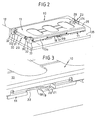
- Fig. 2 shows the contacting device 10 inserted into a device cutout 35, wherein now the lid 13 is shown closed. Since in the closed position of the lid 13 of the lid edge 13a the contact carrier 11 laterally overlaps at least partially, consequently, the contact portion 18 is arranged in a sense "leading". This means that in the closed position of the lid, the contact portion 18 with its contact-determining end portion 20 touch a contact surface 21 and can be supported by spring force on her, which is part of an electronic circuit not otherwise shown.
- the contact surface 21 is, for example, to a trace portion of the ground potential of the electronic circuit.
- the contact section 18 is located on the cover 13 relative to the contact carrier 11 at a position at which the latter has an edge cutout 22. Therefore, the contact portion 18 can be arranged substantially within the outline of the contact carrier 11, so requires no additional space requirement.
- a locking arrangement is also provided, which is designated overall by 23.
- This comprises on the one hand on the contact carrier 11 on its opposite the pivot axis 12 narrow side a locking tab 24 which cooperates in the manner of a clip connection releasably connected to a portion of the front edge 25 of the lid 13.
- the locking takes place by means of a wedge-shaped bolt tongue 26, which projects into the path of movement of the front peripheral edge 25 of the lid 13.
- the latch plate 24 may be integrally-cohesive part of the insulating body 11 of the contact carrier. In the illustrated embodiment is rather thought to form the latch plate 24 on a metal component, in particular for reasons of stability and elasticity.
- FIG. 4 shows the arrangement of a locking tongue 24 consisting of electrically conductive material, in particular metal.
- the locking lug 24 With its anchoring sections 27, the locking lug 24 is injected into the insulating body 14 of the contact carrier 11.
- the ends of the sections 27 are formed as SMD Lötfishchen 28, whereby the latch plate 24 and the rest of the insulating body 11 of the contacting device on the circuit board, so in particular a printed circuit board, attached or can be additionally held.
Landscapes
- Engineering & Computer Science (AREA)
- Physics & Mathematics (AREA)
- General Physics & Mathematics (AREA)
- Theoretical Computer Science (AREA)
- Artificial Intelligence (AREA)
- Computer Vision & Pattern Recognition (AREA)
- Coupling Device And Connection With Printed Circuit (AREA)
- Credit Cards Or The Like (AREA)
- Details Of Connecting Devices For Male And Female Coupling (AREA)
- Shielding Devices Or Components To Electric Or Magnetic Fields (AREA)
Description
- Die Erfindung betrifft eine Kontaktiervorrichtung für eine Chipkarte, insbesondere für eine SIM-Karte, nach dem Oberbegriff des Anspruchs 1.
- Derartige Kontaktiervorrichtungen, in der Umgangssprache und auch in der Patentliteratur häufig unzutreffend mit "Chipkarten-Leser", "SIM-Card-Reader" od. dgl. bezeichnet, dienen zur Halterung und Bereitstellung der elektrischen Kontaktierung der Kontakte einer Chipoder SIM-Karte (SIM = "Subscriber Identity Module") mit Leiterbahnen eines Schaltungsträgers wie insbesondere einer Leiterplatte, die in einem elektronischen Gerät, z.B. einem Mobiltelefon, untergebracht ist.
- Eine Kontaktiervorrichtung solcher Art ist beispielsweise aus
DE 195 21 721 A1 bekannt, von der die vorliegende Erfindung ausgeht. Dabei sind im Kontaktträger neben den sechs üblichen Lesekontakten wenigstens zwei zusätzliche Schaltkontakte untergebracht, die dazu dienen, bei geschlossenem Deckel der Kontaktiervorrichtung, der aus Metall oder metallisiertem Kunststoff besteht, eine Erd- bzw. Masseverbindung zur Leiterplatte herzustellen und dadurch eine den EMV-Forderungen gemäße Schirmung zu ermöglichen. Des weiteren ist im Deckel eine Andruckfeder ausgebildet, die beim Einschieben der SIM-Karte in den geöffneten Deckel in Richtung zum Kontaktträger hin gedrückt wird und die nach Schließen des Deckels, der durch Längsverschieben in eine gesicherte Verriegelungslage verbracht wird, die Schaltkontakte kontaktiert, die sodann, also sequentiell, ihrerseits die Verbindung zur Masse der Leiterplatte herstellen. - Aufgabe vorliegender Erfindung ist insbesondere die Schaffung einer geschirmten Kontaktiervorrichtung, die in ihrem Aufbau vereinfacht ist.
- Die erfindungsgemäße Lösung dieser Aufgabe besteht in den Merkmalen des unabhängigen Anspruchs 1. Dem entsprechend ist eine Kontaktiervorrichtung für eine SIM-Chipkarte eines elektronischen Geräts mit einem Kontaktträger mit darin aufgenommenen Kontaktelementen zur Verbindung der Kontakte der Chipkarte mit Leiterbahnen einer in dem Gerät enthaltenen Leiterplatte, einem elektrisch leitfähigen Deckel, der schwenkbar am Kontaktträger gelagert ist, und eine Aufnahme für die SIM-Karte beinhaltet, und mit einer Einrichtung zur Schirmung durch eine leitende Verbindung zwischen dem Deckel und einer Erd- oder Massekontaktierungsfläche der Leiterplatte dadurch gekennzeichnet, dass der Deckel einen Kontaktabschnitt aufweist, welcher am Kontaktträger vorbei geführt ist oder ihn durchgreift und im geschlossenen Zustand den Erd- oder Massekontakt der Leiterplatte unmittelbar kontaktiert.
- Zweckmäßige und besonders vorteilhafte Weiterbildungen bestehen darin, dass der Kontaktabschnitt aus dem Deckelmaterial ausgebildet ist, wobei der Kontaktabschnitt als federnde Zunge ausgebildet sein kann, die z.B. werkstoffeinheitlich-stoffschlüssig aus dem Deckel, bevorzugt aus dem Randbereich des Deckels, ausgeformt ist. Eine bevorzugte weitere Ausgestaltung besteht darin, dass die Zunge unter dem zur Leiterplatte weisenden, den Kontaktträger flankierenden Rand des Deckels angeordnet ist.
- Ein wesentlicher Vorteil der Erfindung besteht zunächst in der besonderen Einfachheit der Kontaktiervorrichtung, und zwar sowohl hinsichtlich ihres Aufbaus als auch im Hinblick auf eine sichere Funktion. Die Fertigung des Deckels ist gegenüber einem herkömmlichen nicht aufwendiger. Der Kontaktabschnitt kann ohne weiteres bei den ohnehin erforderlichen Stanz-, Schnitt- und Biegevorgängen oder in einem Spritzgieß- bzw. Galvanisierverfahren mit berücksichtigt werden. Auch ein Annieten, Anschweißen od.dgl. des Kontaktabschnitts an den Deckel wäre wenig aufwendig.
- Im Unterschied zum Stand der Technik erfolgt der Masseschluss nicht sequentiell (Deckel - Schaltkontakt; Schaltkontakt - Platine), sondern unmittelbar durch direkte Kontaktierung des Deckels mit dem Massepotential der elektronischen Schaltung. Um dies zu erreichen, ist es lediglich erforderlich, eine Stelle zur Kontaktierung des Massepotentials im Gerätegehäuse frei zu lassen, damit diese Stelle vom deckelseitigen Kontaktabschnitt berührt werden kann. Besondere Kontakte wie die zusätzlichen Schaltkontakte entsprechend
DE 195 21 721 A1 werden nicht benötigt. - Ein weiterer erheblicher Vorteil gegenüber dem in Bezug genommenen Stand der Technik wird darin gesehen, dass die Schirmung auch bei nicht in die Vorrichtung eingesetzter Chipkarte wirksam ist. So ist sichergestellt, dass eine Berührung des elektrisch leitfähigen Deckels, beispielsweise um ihn zum Einsatz einer SIM-Karte zu öffnen, nicht zu einer Beschädigung der Elektronik führen kann, weil auch in diesem Fall elektrostatische Aufladungen zum Massepotential abgeleitet werden.
- Die Erfindung wird nachfolgend unter Bezugnahme auf in den beiliegenden Zeichnungen dargestellte Ausführungsbeispiele näher erläutert. Es zeigen:
- Fig. 1
- eine perspektivische Darstellung einer Kontaktiervorrichtung entsprechend der Erfindung mit einem Kontaktträger und einem teilweise geöffneten Deckel,
- Fig. 2
- eine perspektivische Seitenansicht einer in ein Gerät bzw. Geräteausschnitt eingesetzten Kontaktiervorrichtung bei geschlossenem Deckel,
- Fig. 3
- eine vergrößerte Darstellung einer Einzelheit aus Fig. 2, und
- Fig. 4
- eine perspektivische Darstellung der Kontaktiervorrichtung mit Blickrichtung auf die Lötseite des Kontaktträgers.
- Fig. 1 zeigt eine insgesamt mit 10 bezeichnete Kontaktiervorrichtung für Chip-Karten, insbesondere für SIM-Karten, wie sie beispielsweise in Mobiltelefonen eingesetzt werden.
- Die Kontaktiervorrichtung 10 umfasst einen Kontaktträger 11 und einen um eine Achse 12 schwenkbar daran angelenkten Deckel 13, wobei im dargestellten Ausführungsbeispiel die Schwenkachse 12 einer Schmalseite von Kontaktträger 11 und Deckel 13 zugeordnet ist.
- Im Kontaktträger 11, dessen Korpus 14 aus elektrisch nicht leitendem Isoliermaterial, insbesondere aus Kunststoff besteht, sind - beim Ausführungsbeispiel sechs - Lesekontakte 15 angeordnet zur Kontaktierung mit Kontakten einer nicht dargestellten SIM-Karte, die in bekannter Weise zwischen Kontaktträger 11 und Deckel 13 in die Vorrichtung 10 eingesetzt wird. Mit 16 sind SMD-Lötfüßchen bezeichnet, die stoffschlüssiger Bestandteil der Lesekontakte 15 sind und die galvanische Verbindung zu einem ebenfalls nicht gezeigten Schaltungsträger, also insbesondere einer Leiterplatte dienen.
- Mit 17 ist eine am Kontaktträger 11 angebrachte Kodier-Schrägfläche bezeichnet, die sicherstellt, dass die SIM-Karte, die ihrerseits bekanntermaßen eine entsprechend gebrochene Ecke aufweist, nur mit ihrer korrekten Ausrichtung in die Kontaktiervorrichtung 10 eingesetzt werden kann.
- Der Deckel 13 besteht beim dargestellten Ausführungsbeispiel aus einem Blech-Stanz-Biegeteil, also aus einem elektrisch leitenden Material. Er könnte auch aus anderen leitfähigen Materialen bestehen, z.B. aus elektrisch leitendem oder leitfähig beschichtetem Kunststoff.
- Wie ausgeführt, ist der Deckel 13 an seiner bezüglich Fig. 1 hinteren Schmalkante über die Schwenkachse 12 mit dem Kontaktträger 11 schwenkbar verbunden. Er kann deshalb von einer gegenüber der Darstellung in Fig. 1 noch weiter geöffneten Stellung bis in die Schließstellung verschwenkt werden, die in Fig. 2 dargestellt ist.
- Ein wesentliches Merkmal des Deckels 13 entsprechend der Erfindung besteht zunächst darin, dass er einen Kontaktabschnitt 18 aufweist. Dieser zungenförmige Kontaktabschnitt 18 ist beim Ausführungsbeispiel werkstoffeinheitlich-stoffschlüssiger Bestandteil des Deckels 13, d.h. also insbesondere durch Stanzen und Biegen aus dem Deckel 13 selbst herausgeformt. Wie die Figuren erkennen lassen, ist der Kontaktabschnitt 18 einem aus der Hauptebene des Deckels heruntergebogenen Längsseitenrand 13a des Deckels 13 zugeordnet. Schließlich ist die Anordnung des Kontaktabschnitts 18 so getroffen, dass er innerhalb der zum Kontaktträger 11 weisenden Randkante 13b des Deckelrandes 13a angeordnet ist, dem gegenüber das freie Ende der Zunge 19 mit Richtung zum Kontaktträger 11 hin vorsteht.
- Fig. 2 zeigt die Kontaktiervorrichtung 10 in einen Geräteausschnitt 35 eingesetzt, wobei nun der Deckel 13 geschlossen dargestellt ist. Da in der Schließstellung des Deckels 13 der Deckelrand 13a den Kontaktträger 11 seitlich zumindest teilweise übergreift, ist folglich der Kontaktabschnitt 18 gewissermaßen "voreilend" angeordnet. Das bedeutet, dass in der Schließstellung des Deckels der Kontaktabschnitt 18 mit seinem kontaktierungsbestimmenden Endabschnitt 20 eine Kontaktfläche 21 berühren und sich unter Federkraft auf ihr abstützen kann, die Teil einer ansonsten nicht näher gezeigten elektronischen Schaltung ist. Bei der Kontaktfläche 21 handelt es sich z.B. um einen Leiterbahnabschnitt des Massepotentials der elektronischen Schaltung.
- Wie schließlich aus den Figuren noch zu erkennen ist, befindet sich der Kontaktabschnitt 18 am Deckel 13 relativ zum Kontaktträger 11 an einer Stelle, an der letzterer einen Randausschnitt 22 aufweist. Deshalb kann der Kontaktabschnitt 18 im wesentlichen noch innerhalb des Umrisses des Kontaktträgers 11 angeordnet werden, benötigt also keinen zusätzlichen Flächenbedarf.
- Zur Verriegelung des Deckels 13 in seiner Schließstellung bezüglich des Kontaktträgers 11 ist zudem eine Verriegelungsanordnung vorgesehen, die insgesamt mit 23 bezeichnet ist. Diese umfasst einerseits am Kontaktträger 11 an seiner der Schwenkachse 12 gegenüberliegenden Schmalseite eine Riegellasche 24, die nach Art einer Clipsverbindung wiederlösbar mit einem Abschnitt des vorderen Randes 25 des Deckels 13 zusammenwirkt. Beim dargestellten Ausführungsbeispiel erfolgt die Verriegelung mittels einer keilförmigen Riegelzunge 26, die in die Bewegungsbahn der vorderen Randkante 25 des Deckels 13 hineinragt. Wird der Deckel geschlossen, bewegt seine Vorderkante 25 die federelastisch ausgebildete oder angeordnete Riegellasche 24 vorübergehend ausweichend, bis bei geschlossenem Deckel die Riegelzunge 26 die Deckelrandkante 25 hinterfängt, so wie dies in Fig. 2 dargestellt ist.
- Durch Schließen des Deckels 13 werden die Kontaktkräfte auf die Kontakte 15 aufgebracht und in der Deckelschließstellung sichergestellt. Daraus resultiert für die Schließstellung der Vorrichtung 10, dass die Kontaktkräfte die sichere Verriegelung des Deckels 13 unterstützen.
- Was die an der Stirnkante 25 des Deckels 13 angeordnete Riegellasche 24 betrifft, so sichert diese den Deckel 13 auch gegen ein unerwünschtes Verschieben in Richtung des in Fig. 2 auf die Riegellasche weisenden Pfeils. Eine solche Bewegung könnte ansonsten aufgrund vorhandener Toleranzen möglich sein.
- Soll der Deckel 13 geöffnet werden, drückt man die Riegellasche 24 ein wenig nach außen, bis die Riegelzunge 26 die Deckelrandkante 25 wieder freigibt.
- Die Riegellasche 24 kann einstückig-stoffschlüssiger Bestandteil des Isolierkörpers des Kontaktträgers 11 sein. Beim dargestellten Ausführungsbeispiel ist eher daran gedacht, die Riegellasche 24 an einem Metallbauteil auszubilden, und zwar insbesondere aus Stabilitäts- und Elastizitätsgründen.
- Fig. 4 zeigt die Anordnung einer aus elektrisch leitfähigem Material, insbesondere Metall bestehenden Riegelzunge 24. Mit ihren Verankerungsabschnitten 27 ist die Riegellasche 24 in den Isolierkörper 14 des Kontaktträgers 11 eingespritzt. Die Enden der Abschnitte 27 sind als SMD-Lötfüßchen 28 ausgebildet, womit die Riegellasche 24 und im übrigen auch der Isolierkörper 11 der Kontaktiervorrichtung auf dem Schaltungsträger, also insbesondere einer Leiterplatte, befestigt bzw. zusätzlich gehalten werden kann.
- Was die Aufnahme der SIM-Karte in der Kontaktiervorrichtung 10 betrifft, so ist diese nicht dargestellt. Es ist daran gedacht, wie an sich üblich, an der Unterseite des Deckels 13 - in der Regel durch Randumformungen - eine Führung auszubilden, so dass die SIM-Karte in den Deckel 13 eingeschoben werden kann, bevor dieser geschlossen wird.
Claims (6)
- Kontaktiervorrichtung (10) für eine SIM-Chipkarte eines elektronischen Geräts mit
einem Kontaktträger (11) mit darin aufgenommenen Kontaktelementen (15) zur Verbindung der Kontakte der Chipkarte mit Leiterbahnen einer in dem Gerät enthaltenen Leiterplatte,
einem elektrisch leitfähigen Deckel (13), der
schwenkbar am Kontaktträger (11) gelagert ist, und
eine Aufnahme für die SIM-Karte beinhaltet,
und mit einer Einrichtung zur Schirmung durch eine leitende Verbindung zwischen dem Deckel (13) und einer Erd- oder Massekontaktierungsfläche (21) des Schaltungsträgers,
dadurch gekennzeichnet,
dass der Deckel (13) einen Kontaktabschnitt (18) aufweist, welcher am Kontaktträger (11) vorbei geführt ist oder ihn durchgreift und im geschlossenen Zustand den Erd- oder Massekontakt (21) des Schaltungsträgers unmittelbar kontaktiert. - Kontaktiervorrichtung nach Anspruch 1, dadurch gekennzeichnet, dass der Kontaktabschnitt (18) aus dem Deckelmaterial ausgebildet ist.
- Kontaktiervorrichtung nach Anspruch 2, dadurch gekennzeichnet, dass der Kontaktabschnitt (18) als federnde Zunge (19) ausgebildet ist.
- Kontaktiervorrichtung nach Anspruch 2 oder 3, dadurch gekennzeichnet, dass der Kontaktabschnitt (18) werkstoffeinheitlich-stoffschlüssig aus dem Deckel (13) ausgeformt ist.
- Kontaktiervorrichtung nach Anspruch 3 oder 4, dadurch gekennzeichnet, dass der Kontaktabschnitt (18) aus dem Randbereich (13a) des Deckels (13) herausgeformt ist.
- Kontaktiervorrichtung nach einem der Ansprüche 2 bis 4, dadurch gekennzeichnet, dass der Kontaktabschnitt (18) unter dem zur Leiterplatte weisenden, den Kontaktträger (11) flankierenden Rand (13b) des Deckels (13) angeordnet ist.
Priority Applications (2)
| Application Number | Priority Date | Filing Date | Title |
|---|---|---|---|
| EP05018041A EP1605387B1 (de) | 2002-08-15 | 2003-07-09 | Kontaktiervorrichtung für eine Chipkarte, insbesondere für eine SIM-Karte |
| EP05018042A EP1619603A3 (de) | 2002-08-15 | 2003-07-09 | Kontaktiervorrichtung für eine Chipkarte, insbesondere für eine SIM-Karte |
Applications Claiming Priority (2)
| Application Number | Priority Date | Filing Date | Title |
|---|---|---|---|
| DE10238156A DE10238156A1 (de) | 2002-08-15 | 2002-08-15 | Kontaktiervorrichtung für eine Chipkarte, insbesondere für eine SIM-Karte |
| DE10238156 | 2002-08-15 |
Related Child Applications (2)
| Application Number | Title | Priority Date | Filing Date |
|---|---|---|---|
| EP05018042A Division EP1619603A3 (de) | 2002-08-15 | 2003-07-09 | Kontaktiervorrichtung für eine Chipkarte, insbesondere für eine SIM-Karte |
| EP05018041A Division EP1605387B1 (de) | 2002-08-15 | 2003-07-09 | Kontaktiervorrichtung für eine Chipkarte, insbesondere für eine SIM-Karte |
Publications (3)
| Publication Number | Publication Date |
|---|---|
| EP1398723A2 EP1398723A2 (de) | 2004-03-17 |
| EP1398723A3 EP1398723A3 (de) | 2004-09-01 |
| EP1398723B1 true EP1398723B1 (de) | 2007-08-22 |
Family
ID=31197147
Family Applications (3)
| Application Number | Title | Priority Date | Filing Date |
|---|---|---|---|
| EP05018042A Withdrawn EP1619603A3 (de) | 2002-08-15 | 2003-07-09 | Kontaktiervorrichtung für eine Chipkarte, insbesondere für eine SIM-Karte |
| EP03015425A Expired - Lifetime EP1398723B1 (de) | 2002-08-15 | 2003-07-09 | Kontaktiervorrichtung für eine Chipkarte, insbesondere für eine SIM-Karte |
| EP05018041A Expired - Lifetime EP1605387B1 (de) | 2002-08-15 | 2003-07-09 | Kontaktiervorrichtung für eine Chipkarte, insbesondere für eine SIM-Karte |
Family Applications Before (1)
| Application Number | Title | Priority Date | Filing Date |
|---|---|---|---|
| EP05018042A Withdrawn EP1619603A3 (de) | 2002-08-15 | 2003-07-09 | Kontaktiervorrichtung für eine Chipkarte, insbesondere für eine SIM-Karte |
Family Applications After (1)
| Application Number | Title | Priority Date | Filing Date |
|---|---|---|---|
| EP05018041A Expired - Lifetime EP1605387B1 (de) | 2002-08-15 | 2003-07-09 | Kontaktiervorrichtung für eine Chipkarte, insbesondere für eine SIM-Karte |
Country Status (7)
| Country | Link |
|---|---|
| US (1) | US6863537B2 (de) |
| EP (3) | EP1619603A3 (de) |
| JP (1) | JP3726215B2 (de) |
| CN (1) | CN1279656C (de) |
| AT (1) | ATE371221T1 (de) |
| DE (3) | DE10238156A1 (de) |
| DK (2) | DK1398723T3 (de) |
Cited By (1)
| Publication number | Priority date | Publication date | Assignee | Title |
|---|---|---|---|---|
| DE102020210873A1 (de) | 2020-08-28 | 2022-03-03 | Robert Bosch Gesellschaft mit beschränkter Haftung | Vorrichtung zum Herstellen von Einpressverbindungen zwischen einem oder mehreren Einpresselementen und einem oder mehrere Öffnungen eines Trägers und Verfahren |
Families Citing this family (28)
| Publication number | Priority date | Publication date | Assignee | Title |
|---|---|---|---|---|
| US8246969B2 (en) | 2001-11-16 | 2012-08-21 | Skinmedica, Inc. | Compositions containing aromatic aldehydes and their use in treatments |
| TW200511138A (en) * | 2003-08-26 | 2005-03-16 | Siemens Ag | Card-reading device |
| TWM251345U (en) * | 2003-09-30 | 2004-11-21 | Hon Hai Prec Ind Co Ltd | Electrical card connector |
| FI116325B (fi) * | 2003-12-03 | 2005-10-31 | Nokia Corp | Muistikortin kytkentäelin |
| US7161811B2 (en) * | 2004-03-12 | 2007-01-09 | Lumberg Connect Gmbh & Co. Kg | Card holder for SIM card |
| EP1574984A3 (de) * | 2004-03-12 | 2009-10-21 | Lumberg Connect GmbH | Kontaktiervorrichtung für eine Chipkarte, insbesondere für eine SIM-Karte |
| DE102004015279A1 (de) | 2004-03-29 | 2005-11-03 | Amphenol-Tuchel Electronics Gmbh | Smart Card Connector insbesondere mit Schirmeinrichtung |
| JP4073026B2 (ja) * | 2004-04-06 | 2008-04-09 | 日本航空電子工業株式会社 | カード用コネクタ |
| US20050263596A1 (en) * | 2004-05-12 | 2005-12-01 | Solicore, Inc. | Portable charger, including portable sleeve, for an electronically readable card |
| DE102004054150B4 (de) * | 2004-11-08 | 2007-11-29 | Lumberg Connect Gmbh | Kontaktiervorrichtung für eine Chipkarte, insbesondere für eine SIM- oder USIM-Karte |
| DE102004063982A1 (de) * | 2004-11-09 | 2006-06-14 | Lumberg Connect Gmbh & Co. Kg | Kontaktiervorrichtung für eine Chipkarte, insbesondere für eine SIM-Karte |
| WO2007050078A1 (en) * | 2005-10-26 | 2007-05-03 | University Of North Dakota | High-yield methods for producing low-density microspheres |
| USD528986S1 (en) * | 2005-12-27 | 2006-09-26 | Cheng Uei Precision Industry Co., Ltd. | Memory card connector |
| USD530284S1 (en) * | 2005-12-27 | 2006-10-17 | Cheng Uei Precision Industry Co., Ltd. | SIM card connector |
| DE102006005731B4 (de) | 2006-02-07 | 2007-11-29 | Lumberg Connect Gmbh | Kontaktiervorrichtung für eine Chipkarte |
| DE102006008892B4 (de) * | 2006-02-19 | 2008-04-30 | Gerhard Dipl.-Ing. Richter (FH) | Speicherkartenlesegerät |
| US7361056B1 (en) * | 2006-10-30 | 2008-04-22 | Amphenol East Asia Limited (H.K.) | Micro combined connector structure |
| DE102007031047B4 (de) | 2007-07-04 | 2010-09-09 | Amphenol-Tuchel Electronics Gmbh | Lesegerät für eine Microkarte |
| DE102007031048A1 (de) | 2007-07-04 | 2009-01-15 | Amphenol-Tuchel Electronics Gmbh | Lesegerät für eine elektronische Speicherkarte, insbesondere für eine Microkarte |
| US8047363B2 (en) | 2008-08-26 | 2011-11-01 | Sandisk Technologies Inc. | Memory card holder and organizer for holding and organizing a plurality of portable memory cards |
| USD613293S1 (en) * | 2008-08-26 | 2010-04-06 | Sandisk Corporation | Memory card holder |
| WO2011030176A1 (en) | 2009-09-09 | 2011-03-17 | Sandisk Il Ltd. | Holders for portable memory cards and method for manufacturing same |
| DE102009056391A1 (de) | 2009-11-30 | 2011-06-09 | Amphenol-Tuchel Electronics Gmbh | Lesegerät für eine elektronische Speicherkarte, insbesondere für eine Microkarte |
| USD667829S1 (en) * | 2011-02-18 | 2012-09-25 | Knut Berntsen | Card holder |
| US8753150B2 (en) * | 2011-06-23 | 2014-06-17 | Apple Inc. | Simplified connector receptacles |
| US8292638B1 (en) * | 2011-09-30 | 2012-10-23 | Cheng Uei Precision Industry Co., Ltd. | Two-in-one connector |
| DE102012010294A1 (de) * | 2012-05-24 | 2013-11-28 | Amphenol-Tuchel Electronics Gmbh | Kontaktiervorrichtung |
| JP5718506B1 (ja) * | 2014-04-09 | 2015-05-13 | 日本航空電子工業株式会社 | コネクタ |
Family Cites Families (10)
| Publication number | Priority date | Publication date | Assignee | Title |
|---|---|---|---|---|
| US5257414A (en) * | 1990-11-26 | 1993-10-26 | Motorola, Inc. | Apparatus for accepting and retaining a memory card |
| EP0520080B2 (de) | 1991-06-28 | 2005-03-30 | Molex Incorporated | Verbinder für IC-Karten |
| US5267866A (en) * | 1991-12-17 | 1993-12-07 | Xerox Corporation | Flexible electrical interconnect |
| JP2526500B2 (ja) * | 1993-07-23 | 1996-08-21 | 日本電気株式会社 | 携帯電話機 |
| US5608604A (en) * | 1994-09-22 | 1997-03-04 | Apple Computer, Inc. | Hinge as an electrical conductor |
| DE19521721B4 (de) * | 1995-06-14 | 2006-12-07 | Amphenol-Tuchel Electronics Gmbh | Geschirmte Kontaktiereinrichtung |
| US6149466A (en) * | 1997-05-13 | 2000-11-21 | Itt Manufacturing Enterprises, Inc. | Compact smart card electrical connector |
| US6083010A (en) * | 1998-06-30 | 2000-07-04 | Lucent Technologies, Inc. | Hinge with integrated grounding feature |
| US6074223A (en) * | 1999-04-01 | 2000-06-13 | Hon Hai Precision Ind. Co., Ltd. | Compact flash card having a grounding tab |
| TW474466U (en) * | 2000-06-03 | 2002-01-21 | Hon Hai Prec Ind Co Ltd | Electronic card connector |
-
2002
- 2002-08-15 DE DE10238156A patent/DE10238156A1/de not_active Withdrawn
-
2003
- 2003-07-09 EP EP05018042A patent/EP1619603A3/de not_active Withdrawn
- 2003-07-09 DE DE50307995T patent/DE50307995D1/de not_active Expired - Lifetime
- 2003-07-09 DK DK03015425T patent/DK1398723T3/da active
- 2003-07-09 EP EP03015425A patent/EP1398723B1/de not_active Expired - Lifetime
- 2003-07-09 EP EP05018041A patent/EP1605387B1/de not_active Expired - Lifetime
- 2003-07-09 DE DE50310815T patent/DE50310815D1/de not_active Expired - Lifetime
- 2003-07-09 AT AT03015425T patent/ATE371221T1/de not_active IP Right Cessation
- 2003-07-09 DK DK05018041T patent/DK1605387T3/da active
- 2003-07-18 JP JP2003297927A patent/JP3726215B2/ja not_active Expired - Fee Related
- 2003-08-04 US US10/633,883 patent/US6863537B2/en not_active Expired - Fee Related
- 2003-08-15 CN CN03154529.7A patent/CN1279656C/zh not_active Expired - Fee Related
Cited By (2)
| Publication number | Priority date | Publication date | Assignee | Title |
|---|---|---|---|---|
| DE102020210873A1 (de) | 2020-08-28 | 2022-03-03 | Robert Bosch Gesellschaft mit beschränkter Haftung | Vorrichtung zum Herstellen von Einpressverbindungen zwischen einem oder mehreren Einpresselementen und einem oder mehrere Öffnungen eines Trägers und Verfahren |
| DE102020210873B4 (de) | 2020-08-28 | 2022-03-17 | Robert Bosch Gesellschaft mit beschränkter Haftung | Vorrichtung zum Herstellen von Einpressverbindungen zwischen einem oder mehreren Einpresselementen und einem oder mehrere Öffnungen eines Trägers und Verfahren |
Also Published As
| Publication number | Publication date |
|---|---|
| JP2004078968A (ja) | 2004-03-11 |
| US6863537B2 (en) | 2005-03-08 |
| DK1605387T3 (da) | 2009-02-23 |
| EP1619603A3 (de) | 2008-04-02 |
| ATE371221T1 (de) | 2007-09-15 |
| CN1479414A (zh) | 2004-03-03 |
| EP1605387A3 (de) | 2008-04-02 |
| JP3726215B2 (ja) | 2005-12-14 |
| DK1398723T3 (da) | 2007-09-17 |
| EP1619603A2 (de) | 2006-01-25 |
| EP1605387A2 (de) | 2005-12-14 |
| EP1398723A2 (de) | 2004-03-17 |
| EP1398723A3 (de) | 2004-09-01 |
| HK1061926A1 (en) | 2004-10-08 |
| DE10238156A1 (de) | 2004-03-04 |
| DE50310815D1 (de) | 2009-01-02 |
| EP1605387B1 (de) | 2008-11-19 |
| CN1279656C (zh) | 2006-10-11 |
| US20040058576A1 (en) | 2004-03-25 |
| DE50307995D1 (de) | 2007-10-04 |
Similar Documents
| Publication | Publication Date | Title |
|---|---|---|
| EP1605387B1 (de) | Kontaktiervorrichtung für eine Chipkarte, insbesondere für eine SIM-Karte | |
| DE60221309T2 (de) | Flash-Speicherkarteverbinder, Verbinderanordnung mit dem Verbinder und elektronisches Gerät mit der Verbinderanordnung | |
| DE19521721B4 (de) | Geschirmte Kontaktiereinrichtung | |
| DE69104350T2 (de) | Verbinder für IC-Karten. | |
| DE69835506T2 (de) | Verbinder für IC-Karten | |
| DE4417088C2 (de) | Kontaktiersystem für Chipkarten | |
| DE69827750T2 (de) | Miniaturkarten-annahmeverbinder | |
| EP0735507A2 (de) | Kontaktiereinheit für kartenförmige Trägerelemente | |
| DE19947162C1 (de) | Steckkarte für elektronische Geräte | |
| EP0911749B1 (de) | Chipkarten-Kontaktiereinheit | |
| EP1655686B1 (de) | Kontaktvorrichtung für eine Chipkarte, insbesondere für eine SIM- oder USIM-Karte | |
| EP1655685A2 (de) | Kontaktiervorrichtung für eine Chipkarte, insbesondere für eine SIM-Karte | |
| EP1553663B1 (de) | Kontaktiereinheit für ein kartenförmiges Trägerelement elektronischer Baugruppen | |
| EP1738294B1 (de) | Smart card connector insbesondere mit schirmeinrichtung | |
| EP1172832A2 (de) | Tastatur, vorzugsweise für Datenkassen | |
| DE60028674T2 (de) | Ic-Karte mit ausziehbarer Ablage | |
| EP1414283B1 (de) | Elektronische Steuereinrichtung mit Mitteln zur Ableitung von Störsignalen | |
| EP0833271A2 (de) | Kartenlesevorrichtung | |
| DE102007057521B4 (de) | Smart-Card-Connector mit Schirmeinrichtung | |
| DE102009011638B4 (de) | Tragbarer Computer | |
| DE20212809U1 (de) | Kontaktiervorrichtung für eine Chipkarte, insbesondere für eine SIM-Karte | |
| DE102006041931B4 (de) | Kontaktiervorrichtung für eine Chipkarte, insbesondere für eine SIM-Karte | |
| DE102004054270B4 (de) | Kontaktiervorrichtung für eine Chipkarte, insbesondere für eine SIM-Karte | |
| DE102004032104B4 (de) | Kontaktiereinheit zum Lesen und/oder Beschreiben von Chipkarten | |
| DE202004017395U1 (de) | Kontaktiervorrichtung für eine Chipkarte, insbesondere für eine SIM-Karte |
Legal Events
| Date | Code | Title | Description |
|---|---|---|---|
| PUAI | Public reference made under article 153(3) epc to a published international application that has entered the european phase |
Free format text: ORIGINAL CODE: 0009012 |
|
| AK | Designated contracting states |
Kind code of ref document: A2 Designated state(s): AT BE BG CH CY CZ DE DK EE ES FI FR GB GR HU IE IT LI LU MC NL PT RO SE SI SK TR |
|
| AX | Request for extension of the european patent |
Extension state: AL LT LV MK |
|
| PUAL | Search report despatched |
Free format text: ORIGINAL CODE: 0009013 |
|
| RIC1 | Information provided on ipc code assigned before grant |
Ipc: 7H 01R 13/24 B Ipc: 7G 06K 7/00 A Ipc: 7G 06K 13/08 B |
|
| AK | Designated contracting states |
Kind code of ref document: A3 Designated state(s): AT BE BG CH CY CZ DE DK EE ES FI FR GB GR HU IE IT LI LU MC NL PT RO SE SI SK TR |
|
| AX | Request for extension of the european patent |
Extension state: AL LT LV MK |
|
| 17P | Request for examination filed |
Effective date: 20040813 |
|
| 17Q | First examination report despatched |
Effective date: 20050222 |
|
| AKX | Designation fees paid |
Designated state(s): AT BE BG CH CY CZ DE DK EE ES FI FR GB GR HU IE IT LI LU MC NL PT RO SE SI SK TR |
|
| GRAP | Despatch of communication of intention to grant a patent |
Free format text: ORIGINAL CODE: EPIDOSNIGR1 |
|
| RAP1 | Party data changed (applicant data changed or rights of an application transferred) |
Owner name: LUMBERG CONNECT GMBH |
|
| GRAS | Grant fee paid |
Free format text: ORIGINAL CODE: EPIDOSNIGR3 |
|
| GRAA | (expected) grant |
Free format text: ORIGINAL CODE: 0009210 |
|
| AK | Designated contracting states |
Kind code of ref document: B1 Designated state(s): AT BE BG CH CY CZ DE DK EE ES FI FR GB GR HU IE IT LI LU MC NL PT RO SE SI SK TR |
|
| REG | Reference to a national code |
Ref country code: GB Ref legal event code: FG4D Free format text: NOT ENGLISH |
|
| REG | Reference to a national code |
Ref country code: SE Ref legal event code: TRGR |
|
| REG | Reference to a national code |
Ref country code: CH Ref legal event code: EP |
|
| REG | Reference to a national code |
Ref country code: DK Ref legal event code: T3 |
|
| REG | Reference to a national code |
Ref country code: IE Ref legal event code: FG4D Free format text: LANGUAGE OF EP DOCUMENT: GERMAN |
|
| REF | Corresponds to: |
Ref document number: 50307995 Country of ref document: DE Date of ref document: 20071004 Kind code of ref document: P |
|
| PG25 | Lapsed in a contracting state [announced via postgrant information from national office to epo] |
Ref country code: BG Free format text: LAPSE BECAUSE OF FAILURE TO SUBMIT A TRANSLATION OF THE DESCRIPTION OR TO PAY THE FEE WITHIN THE PRESCRIBED TIME-LIMIT Effective date: 20071122 Ref country code: NL Free format text: LAPSE BECAUSE OF FAILURE TO SUBMIT A TRANSLATION OF THE DESCRIPTION OR TO PAY THE FEE WITHIN THE PRESCRIBED TIME-LIMIT Effective date: 20070822 Ref country code: ES Free format text: LAPSE BECAUSE OF FAILURE TO SUBMIT A TRANSLATION OF THE DESCRIPTION OR TO PAY THE FEE WITHIN THE PRESCRIBED TIME-LIMIT Effective date: 20071203 |
|
| NLV1 | Nl: lapsed or annulled due to failure to fulfill the requirements of art. 29p and 29m of the patents act | ||
| GBV | Gb: ep patent (uk) treated as always having been void in accordance with gb section 77(7)/1977 [no translation filed] |
Effective date: 20070822 |
|
| REG | Reference to a national code |
Ref country code: IE Ref legal event code: FD4D |
|
| EN | Fr: translation not filed | ||
| PG25 | Lapsed in a contracting state [announced via postgrant information from national office to epo] |
Ref country code: GR Free format text: LAPSE BECAUSE OF FAILURE TO SUBMIT A TRANSLATION OF THE DESCRIPTION OR TO PAY THE FEE WITHIN THE PRESCRIBED TIME-LIMIT Effective date: 20071123 |
|
| PG25 | Lapsed in a contracting state [announced via postgrant information from national office to epo] |
Ref country code: SK Free format text: LAPSE BECAUSE OF FAILURE TO SUBMIT A TRANSLATION OF THE DESCRIPTION OR TO PAY THE FEE WITHIN THE PRESCRIBED TIME-LIMIT Effective date: 20070822 Ref country code: GB Free format text: LAPSE BECAUSE OF FAILURE TO SUBMIT A TRANSLATION OF THE DESCRIPTION OR TO PAY THE FEE WITHIN THE PRESCRIBED TIME-LIMIT Effective date: 20070822 Ref country code: IE Free format text: LAPSE BECAUSE OF FAILURE TO SUBMIT A TRANSLATION OF THE DESCRIPTION OR TO PAY THE FEE WITHIN THE PRESCRIBED TIME-LIMIT Effective date: 20070822 Ref country code: PT Free format text: LAPSE BECAUSE OF FAILURE TO SUBMIT A TRANSLATION OF THE DESCRIPTION OR TO PAY THE FEE WITHIN THE PRESCRIBED TIME-LIMIT Effective date: 20080122 |
|
| PLBE | No opposition filed within time limit |
Free format text: ORIGINAL CODE: 0009261 |
|
| STAA | Information on the status of an ep patent application or granted ep patent |
Free format text: STATUS: NO OPPOSITION FILED WITHIN TIME LIMIT |
|
| PG25 | Lapsed in a contracting state [announced via postgrant information from national office to epo] |
Ref country code: RO Free format text: LAPSE BECAUSE OF FAILURE TO SUBMIT A TRANSLATION OF THE DESCRIPTION OR TO PAY THE FEE WITHIN THE PRESCRIBED TIME-LIMIT Effective date: 20070822 |
|
| 26N | No opposition filed |
Effective date: 20080526 |
|
| PGFP | Annual fee paid to national office [announced via postgrant information from national office to epo] |
Ref country code: CZ Payment date: 20080624 Year of fee payment: 6 |
|
| PGFP | Annual fee paid to national office [announced via postgrant information from national office to epo] |
Ref country code: DK Payment date: 20080717 Year of fee payment: 6 |
|
| PGFP | Annual fee paid to national office [announced via postgrant information from national office to epo] |
Ref country code: IT Payment date: 20080627 Year of fee payment: 6 |
|
| REG | Reference to a national code |
Ref country code: CH Ref legal event code: PL |
|
| PG25 | Lapsed in a contracting state [announced via postgrant information from national office to epo] |
Ref country code: MC Free format text: LAPSE BECAUSE OF NON-PAYMENT OF DUE FEES Effective date: 20080731 |
|
| PG25 | Lapsed in a contracting state [announced via postgrant information from national office to epo] |
Ref country code: EE Free format text: LAPSE BECAUSE OF FAILURE TO SUBMIT A TRANSLATION OF THE DESCRIPTION OR TO PAY THE FEE WITHIN THE PRESCRIBED TIME-LIMIT Effective date: 20070822 |
|
| PG25 | Lapsed in a contracting state [announced via postgrant information from national office to epo] |
Ref country code: LI Free format text: LAPSE BECAUSE OF NON-PAYMENT OF DUE FEES Effective date: 20080731 Ref country code: CH Free format text: LAPSE BECAUSE OF NON-PAYMENT OF DUE FEES Effective date: 20080731 Ref country code: SI Free format text: LAPSE BECAUSE OF FAILURE TO SUBMIT A TRANSLATION OF THE DESCRIPTION OR TO PAY THE FEE WITHIN THE PRESCRIBED TIME-LIMIT Effective date: 20070822 |
|
| PG25 | Lapsed in a contracting state [announced via postgrant information from national office to epo] |
Ref country code: CY Free format text: LAPSE BECAUSE OF FAILURE TO SUBMIT A TRANSLATION OF THE DESCRIPTION OR TO PAY THE FEE WITHIN THE PRESCRIBED TIME-LIMIT Effective date: 20070822 |
|
| PG25 | Lapsed in a contracting state [announced via postgrant information from national office to epo] |
Ref country code: AT Free format text: LAPSE BECAUSE OF NON-PAYMENT OF DUE FEES Effective date: 20080709 |
|
| REG | Reference to a national code |
Ref country code: DK Ref legal event code: EBP |
|
| PG25 | Lapsed in a contracting state [announced via postgrant information from national office to epo] |
Ref country code: CZ Free format text: LAPSE BECAUSE OF NON-PAYMENT OF DUE FEES Effective date: 20090709 |
|
| PG25 | Lapsed in a contracting state [announced via postgrant information from national office to epo] |
Ref country code: HU Free format text: LAPSE BECAUSE OF FAILURE TO SUBMIT A TRANSLATION OF THE DESCRIPTION OR TO PAY THE FEE WITHIN THE PRESCRIBED TIME-LIMIT Effective date: 20080223 Ref country code: LU Free format text: LAPSE BECAUSE OF NON-PAYMENT OF DUE FEES Effective date: 20080709 Ref country code: BE Free format text: LAPSE BECAUSE OF NON-PAYMENT OF DUE FEES Effective date: 20080731 Ref country code: DK Free format text: LAPSE BECAUSE OF NON-PAYMENT OF DUE FEES Effective date: 20090731 |
|
| PG25 | Lapsed in a contracting state [announced via postgrant information from national office to epo] |
Ref country code: TR Free format text: LAPSE BECAUSE OF FAILURE TO SUBMIT A TRANSLATION OF THE DESCRIPTION OR TO PAY THE FEE WITHIN THE PRESCRIBED TIME-LIMIT Effective date: 20070822 |
|
| PG25 | Lapsed in a contracting state [announced via postgrant information from national office to epo] |
Ref country code: IT Free format text: LAPSE BECAUSE OF NON-PAYMENT OF DUE FEES Effective date: 20090709 |
|
| PGFP | Annual fee paid to national office [announced via postgrant information from national office to epo] |
Ref country code: SE Payment date: 20110722 Year of fee payment: 9 Ref country code: FI Payment date: 20110706 Year of fee payment: 9 Ref country code: DE Payment date: 20110530 Year of fee payment: 9 |
|
| REG | Reference to a national code |
Ref country code: DE Ref legal event code: R082 Ref document number: 50307995 Country of ref document: DE Representative=s name: PATENTANWAELTE OSTRIGA, SONNET, WIRTHS & VORWE, DE |
|
| PG25 | Lapsed in a contracting state [announced via postgrant information from national office to epo] |
Ref country code: FR Free format text: LAPSE BECAUSE OF FAILURE TO SUBMIT A TRANSLATION OF THE DESCRIPTION OR TO PAY THE FEE WITHIN THE PRESCRIBED TIME-LIMIT Effective date: 20080418 |
|
| REG | Reference to a national code |
Ref country code: SE Ref legal event code: EUG |
|
| PG25 | Lapsed in a contracting state [announced via postgrant information from national office to epo] |
Ref country code: FI Free format text: LAPSE BECAUSE OF NON-PAYMENT OF DUE FEES Effective date: 20120709 Ref country code: SE Free format text: LAPSE BECAUSE OF NON-PAYMENT OF DUE FEES Effective date: 20120710 Ref country code: DE Free format text: LAPSE BECAUSE OF NON-PAYMENT OF DUE FEES Effective date: 20130201 |
|
| REG | Reference to a national code |
Ref country code: DE Ref legal event code: R119 Ref document number: 50307995 Country of ref document: DE Effective date: 20130201 |