EP1394842A1 - Thin film forming apparatus cleaning method - Google Patents
Thin film forming apparatus cleaning method Download PDFInfo
- Publication number
- EP1394842A1 EP1394842A1 EP02700635A EP02700635A EP1394842A1 EP 1394842 A1 EP1394842 A1 EP 1394842A1 EP 02700635 A EP02700635 A EP 02700635A EP 02700635 A EP02700635 A EP 02700635A EP 1394842 A1 EP1394842 A1 EP 1394842A1
- Authority
- EP
- European Patent Office
- Prior art keywords
- gas
- cleaning
- thin film
- film deposition
- deposition apparatus
- Prior art date
- Legal status (The legal status is an assumption and is not a legal conclusion. Google has not performed a legal analysis and makes no representation as to the accuracy of the status listed.)
- Granted
Links
Images




Classifications
-
- C—CHEMISTRY; METALLURGY
- C23—COATING METALLIC MATERIAL; COATING MATERIAL WITH METALLIC MATERIAL; CHEMICAL SURFACE TREATMENT; DIFFUSION TREATMENT OF METALLIC MATERIAL; COATING BY VACUUM EVAPORATION, BY SPUTTERING, BY ION IMPLANTATION OR BY CHEMICAL VAPOUR DEPOSITION, IN GENERAL; INHIBITING CORROSION OF METALLIC MATERIAL OR INCRUSTATION IN GENERAL
- C23C—COATING METALLIC MATERIAL; COATING MATERIAL WITH METALLIC MATERIAL; SURFACE TREATMENT OF METALLIC MATERIAL BY DIFFUSION INTO THE SURFACE, BY CHEMICAL CONVERSION OR SUBSTITUTION; COATING BY VACUUM EVAPORATION, BY SPUTTERING, BY ION IMPLANTATION OR BY CHEMICAL VAPOUR DEPOSITION, IN GENERAL
- C23C16/00—Chemical coating by decomposition of gaseous compounds, without leaving reaction products of surface material in the coating, i.e. chemical vapour deposition [CVD] processes
- C23C16/44—Chemical coating by decomposition of gaseous compounds, without leaving reaction products of surface material in the coating, i.e. chemical vapour deposition [CVD] processes characterised by the method of coating
- C23C16/4401—Means for minimising impurities, e.g. dust, moisture or residual gas, in the reaction chamber
- C23C16/4405—Cleaning of reactor or parts inside the reactor by using reactive gases
-
- H—ELECTRICITY
- H10—SEMICONDUCTOR DEVICES; ELECTRIC SOLID-STATE DEVICES NOT OTHERWISE PROVIDED FOR
- H10P—GENERIC PROCESSES OR APPARATUS FOR THE MANUFACTURE OR TREATMENT OF DEVICES COVERED BY CLASS H10
- H10P14/00—Formation of materials, e.g. in the shape of layers or pillars
- H10P14/20—Formation of materials, e.g. in the shape of layers or pillars of semiconductor materials
Definitions
- the present invention relates to a thin film deposition apparatus cleaning method and, more specifically, to a thin film deposition apparatus cleaning method, for removing deposits deposited on the inner surface of the thin film deposition apparatus during a process for forming a thin film on a workpiece, such as a semiconductor wafer.
- a semiconductor device fabricating procedure includes a thin film deposition process, such as a CVD process (chemical vapor deposition process), for forming a thin film, such as a silicon dioxide film, a silicon nitride film or the like, on a workpiece, such as a semiconductor wafer.
- a thin film deposition process uses a thermal processing apparatus as shown in Fig. 15 to form a thin film on a semiconductor wafer by the following procedure.
- a heater 53 heats a double-wall reaction tube 52 consisting of an inner tube 52a and an outer tube 52b at a predetermined temperature.
- a wafer boat 55 holding a plurality of semiconductor wafers 54 is loaded into the reaction tube 52 (inner tube 52a). Gases in the reaction tube 52 are discharged through an exhaust port 56 to set the interior of the reaction tube 52 at a predetermined reduced pressure. After the interior of the reaction tube 52 has been set at the predetermined reduced pressure, process gases are supplied through a gas supply pipe 57 into the inner tube 52a. The process gases undergo a thermal reaction, and a reaction product produced by the thermal reaction deposits on the surfaces of the semiconductor wafers 54 to form thin films on the surfaces of the semiconductor wafers 54.
- Waste gases produced by the thin film deposition process are discharged outside the thermal processing unit 51 through an exhaust pipe 58 connected to the exhaust port 56.
- a trap and a scrubber and such, not shown, are placed in the exhaust pipe 58. The trap removes the reaction product and other substances contained in the waste gases to discharge the waste gases from the thermal processing unit 51 after rendering the waste gases harmless.
- the reaction product produced by the thin film deposition process deposits not only on (adheres not only to) the surfaces of the semiconductor wafers 54, but also on (but also to) the inner surfaces of the thermal processing unit 51 including the inner surface of the inner tube 52a and the surfaces of jigs. If the thin film deposition process is continued in the thermal processing unit 51 with the reaction product adhering to the inside surfaces of the thermal processing unit 51, the reaction product will eventually come off and produce particles. The particles contaminate the semiconductor wafers 54, which reduces the yield of semiconductor devices which are manufactured using the semiconductor wafers 54 contaminated with those particles.
- a cleaning process is carried out after the thin film deposition process has been repeated several times to clean the thermal processing unit 51.
- the cleaning process heats the reaction tube 52 at a predetermined temperature by the heater 53, supplies a cleaning gas, such as a fluoride gas, into the heated reaction tube 52 to remove by etching the reaction product adhering to the inner surfaces of the thermal processing unit 51.
- a cleaning gas such as a fluoride gas
- the fluoride gas for such a purpose is a perfluorocompound, such as CF 4 , C 2 F 6 , NF 3 or SF 6 .
- the perfluorocompond has a long life. For example, CF 4 lasts 50,000 years or longer.
- the emission of the perfluorocompound into the atmosphere causes global warming. Since there is the possibility that the use of the fluoride gas as a cleaning gas negatively affects the global environment, studies have been made to use a cleaning gas other than the perfluorocompound, such as fluorine gas (F 2 ).
- the interior of the reaction tube 52 must be heated at the predetermined temperature to make the cleaning gas etch the reaction product at a desired etch rate to remove the reaction product deposited on the inner surfaces of the thermal processing unit 51.
- the interior of the reaction tube 52 needs to be heated at a high temperature of, for example, 400°C, to etch the deposited reaction product at a desired etch rate using fluorine gas as a cleaning gas.
- reaction tube 52 formed of quartz and the jigs formed of silicon carbide (SiC) are etched at etch rates higher than that at which the reaction product is etched, and reaction product selectivity, i.e., the ratio between etch rates for the reaction product and the material, decreases. Consequently, the reaction tube 52 formed of quartz, and the jigs formed of SiC are deteriorated when the reaction deposit is removed.
- the present invention has been made in view of the foregoing problems and it is therefore an object of the present invention to provide a thin film deposition apparatus cleaning method capable of removing deposits deposited inside the thin film deposition apparatus, suppressing the deterioration of a reaction vessel and jigs.
- Another object of the present invention is to provide a thin film deposition apparatus cleaning method capable of etching deposits deposited inside the thin film deposition apparatus at a high etch rate.
- a third object of the present invention to provide a thin film deposition apparatus cleaning method capable of removing deposits deposited inside the thin film deposition apparatus with the interior of a reaction vessel heated at a low temperature.
- a thin film deposition apparatus cleaning method of cleaning a thin film deposition apparatus by removing deposits adhering to an inner surfaces of the thin film deposition apparatus after depositing thin films on workpieces by supplying a process gas into a reaction vessel included in the thin film deposition apparatus comprises the steps of: heating an interior of the reaction vessel at a predetermined temperature; and cleaning an interior of the thin film deposition apparatus by supplying a cleaning gas containing fluorine gas and an additive gas capable of promoting the activation of the fluorine gas into the reaction vessel heated at the predetermined temperature, heating the cleaning gas at a predetermined temperature to activate the fluorine gas contained in the cleaning gas, and removing the deposits with the activated fluorine gas.
- the cleaning gas is supplied into the reaction vessel heated at the predetermined temperature, the cleaning gas supplied into the reaction vessel is heated at the predetermined temperature, and thereby the fluorine gas contained in the cleaning gas is activated. Since the cleaning gas contains the additive gas capable of activating the fluorine gas, the activation of the fluorine gas is promoted. Since the activation of the fluorine gas is thus promoted, the deposits adhering to the interior of the thin film deposition apparatus can be etched at a high etch rate. The etch rate for the deposits is high and hence the temperature in the reaction vessel may be low. Thus, the temperature in the reaction vessel may be low during the removal of deposits deposited in the thin film deposition apparatus.
- the deposits are removed and the interior of the thin film deposition apparatus is cleaned by supplying the cleaning gas containing fluorine gas and the additive gas capable of promoting the activation of the fluorine gas and of increasing the etch rate for the deposits without decreasing selectivity, i.e., the ratio of the etch rate for the deposit to that for the materials forming the internal members of the thin film deposition apparatus, into the reaction vessel in the cleaning step.
- the cleaning gas supplied into the reaction vessel etches the deposits at a high etch rate without decreasing selectivity with respect to the materials forming the internal members of the thin film deposition apparatus owing to the agency of the additive gas. Consequently, the deposits deposited in the thin film deposition apparatus can be removed, suppressing the deterioration of the internal members of the thin film deposition apparatus, such as the reaction vessel and the jigs.
- chlorine gas hydrogen fluoride gas, ammonia gas or hydrogen gas is used as an additive gas.
- the deposits to are removed to clean the interior of the thin film deposition apparatus by supplying a cleaning gas containing fluorine gas and chlorine gas into the reaction vessel heated at the predetermined temperature in the cleaning step.
- the cleaning gas contains fluorine gas and chlorine gas, and etches the deposits at a high etch rate without decreasing selectivity with respect to the materials forming the internal members of the thin film deposition apparatus. Consequently, the deposits deposited in the thin film deposition apparatus can be removed, suppressing the deterioration of the internal members of the thin film deposition apparatus, such as the reaction vessel and the jigs.
- the deposits are removed to clean the interior of the thin film deposition apparatus by supplying a cleaning gas containing fluorine gas and hydrogen fluoride gas into the reaction vessel heated at a predetermined temperature in the cleaning step.
- the cleaning gas contains fluorine gas and hydrogen fluoride gas
- the deposits are etched at a high etch rate without decreasing selectivity with respect to the materials forming the internal members of the thin film deposition apparatus. Consequently, the deposits deposited in the thin film deposition apparatus are removed, suppressing the deterioration of the reaction vessel and the jigs.
- the cleaning gas containing fluorine gas and hydrogen fluoride gas supplied such that the flow rate ratio between fluorine gas is supplied and hydrogen fluoride gas is in the range of 1 : 3 to 3 : 1.
- fluorine gas and hydrogen fluoride gas of the cleaning gas When fluorine gas and hydrogen fluoride gas of the cleaning gas is supplied such that the flow rate ratio between fluorine gas and hydrogen fluoride gas is in the range of 1 : 3 to 1 : 1, the etch rate for the deposits deposited in the thin film deposition apparatus, and selectivity with respect to the materials forming the internal members of the thin film deposition apparatus are high.
- the cleaning gas containing fluorine gas and hydrogen fluoride gas is supplied such that the flow rate ratio between fluorine gas are supplied and hydrogen fluoride gas is 1 : 1.
- fluorine gas and hydrogen fluoride gas are supplied respectively at flow rates not lower than 2 l/min.
- the deposits deposited in the thin film deposition apparatus is etched at a high etch rate, and selectivity with respect to quartz is high.
- the deposits are removed to clean the interior of the thin film deposition apparatus by supplying a cleaning gas containing fluorine gas and ammonia gas into a reaction vessel heated at a predetermined temperature.
- the cleaning gas containing fluorine gas and ammonia gas etches the deposits at a high etch rate without decreasing selectivity with respect to the materials forming the internal members of the thin film deposition apparatus. Consequently, the deposits deposited in the thin film deposition apparatus are removed, suppressing the deterioration of the reaction vessel and the jigs.
- the cleaning gas containing fluorine gas and ammonia gas is supplied such that the flow rate ratio between fluorine gas and ammonia gas is in the range of 2 : 1 to 10 : 1.
- the deposits deposited in the thin film deposition apparatus are etched at a high etch rate, and selectivity with respect to the materials forming the internal members of the thin film deposition apparatus is high.
- the deposits are removed to clean the interior of the thin film deposition apparatus by supplying a cleaning gas containing fluorine gas and hydrogen gas is supplied into the reaction vessel heated at a predetermined temperature in the cleaning step.
- the cleaning gas containing fluorine gas and hydrogen gas etches the deposits at a high etch rate without decreasing selectivity with respect to the materials forming the internal members of the thin film deposition apparatus. Consequently, the deposits deposited in the thin film deposition apparatus are removed, suppressing the deterioration of the reaction vessel and the jigs.
- the cleaning gas containing fluorine gas and hydrogen gas is supplied such that the flow rate ratio between fluorine gas and hydrogen gas is in the range of 5 : 1 to 5 : 3.
- the deposits deposited in the thin film deposition apparatus are etched at a high etch rate, and selectivity with respect to the materials forming the internal members of the thin film deposition apparatus is high. Silicon nitride can be etched at a high etch rate even if the flow rate of hydrogen gas is not controlled precisely. Consequently, the flow rate of hydrogen gas can easily be controlled.
- the cleaning gas containing fluorine gas and hydrogen gas is supplied such that the flow rate ratio between fluorine gas and hydrogen gas is 5 : 3.
- the etch rate for quartz generally used for forming reaction vessels is low, so that the deposits deposited in the thin film deposition apparatus can be removed, suppressing the deterioration of the reaction vessel.
- the materials forming the internal members of the thin film deposition apparatus include at least either quartz or silicon carbide.
- the interior of the reaction vessel is heated at a temperature below 400°C in the heating step.
- the interior of the reaction vessel is heated at a temperature in the range of 250°C to 380°C in the heating step.
- the deposits can be etched at a high etch rate, while suppressing the deterioration of the reaction vessel and the jigs.
- the cleaning gas is diluted with a diluent gas to produce a diluted cleaning gas, and the diluted cleaning gas is supplied into the reaction vessel.
- the thin film deposition apparatus cleaning method of the present invention uses an inert gas is used as the diluent gas.
- silicon nitride films are formed on the workpieces, and in the cleaning step silicon nitride deposited in the thin film deposition apparatus is removed, when depositing the silicon nitride films on the workpieces with the cleaning gas.
- a thin film deposition apparatus cleaning method of cleaning a thin film deposition apparatus by removing deposits adhering to the inner surface of an exhaust pipe after forming thin films on workpieces by supplying a process gas in a reaction vessel included in the thin film deposition apparatus and discharging gases from the reaction vessel in to the exhaust pipe comprises the steps of: heating an interior of the exhaust pipe at a predetermined temperature; and cleaning an interior of the exhaust pipe by supplying a cleaning gas containing fluorine gas and an additive gas capable of promoting the activation of the fluorine gas into the exhaust pipe heated at the predetermined temperature in the heating step, heating the cleaning gas at a predetermined temperature to activate the fluorine gas contained in the cleaning gas, and removing the' deposits with the activated fluorine gas.
- the cleaning gas is supplied through the reaction vessel into the exhaust pipe.
- the cleaning gas is supplied through an inlet port formed in the exhaust pipe into the exhaust pipe.
- a thin film deposition apparatus cleaning method in a preferred embodiment according to the present invention will be described as applied to cleaning a batch-furnace vertical thermal processing apparatus (thin film deposition apparatus) 1 shown in Fig. 1.
- the thermal processing apparatus 1 (thin film deposition apparatus) 1 to which this embodiment is applied will be described.
- the thermal processing apparatus 1 has a substantially cylindrical reaction tube (reaction vessel) 2 in a vertical position, and an exhaust pipe 17 for carrying gases discharged from the reaction tube 2.
- the reaction tube (reaction vessel) 2 is a double-wall structure consisting of an inner tube 3, and a topped outer tube 4 covering the inner tube'3 so that an annular space is defined between the inner tube 3 and the outer tube 4.
- the inner tube 3 and the outer tube 4 are formed of a heat-resistant material, such as quartz.
- the outer tube 4 is mounted on a manifold 5 formed of a stainless steel (SUS).
- the manifold 5 is joined airtightly to the lower end of the outer tube 4.
- the inner tube 3 is supported on a support ring 6 formed integrally with the manifold 5 so as to protrude from the inner circumference of the manifold 5.
- a cover 7 is disposed under the manifold 5.
- a boat elevator 8 moves the cover 7 vertically. The boat elevator 8 raises the cover 7 to close the bottom of the manifold 5.
- a wafer boat 9 formed of, for example, quartz is mounted on the cover 7.
- the wafer boat 9 is capable of holding a plurality of workpieces, for example, semiconductor wafers 10 at predetermined spacing in a vertical arrangement.
- a heat-insulating member 11 is provided to surround the reaction tube 2.
- a heater 12 having a resistive heating element is attached to the inner surface of the side wall of the heat-insulating member 11.
- a plurality of process gas supply pipes 13 are connected to the side wall of the manifold 5. Only one of the process gas supply pipes 13 is shown in Fig. 1.
- the process gas supply pipes 13 is open into the inner tube 3.
- the process gas supply pipes 13 are connected to parts, below the support ring 6 (below the inner tube 3), of the side wall of the manifold 5. Process gases are introduced through the process gas supply pipes 13 into the inner tube 3 so as to be delivered to the semiconductor wafers 10.
- a cleaning gas supply pipe 14 is connected to the side wall of the manifold 5 so as to open into the inner tube 3. A cleaning gas is introduced through the cleaning gas supply pipe 14 into the inner tube 3.
- An exhaust port 15 is formed in a part, above the support ring 6, of the side wall of the manifold 5 so as to be open into the annular space between the inner tube 3 and the outer tube 4 of the reaction tube 2. Waste gases produced inside the inner tube 3 are discharged through the annular space between the inner tube 3 and the outer tube 4, and the exhaust port 15.
- a purge gas supply pipe 16 is connected to a part, below the exhaust port 15, of the side wall of the manifold 15 to supply nitrogen gas as a purge gas into the reaction tube 2.
- the exhaust pipe 17 is connected airtightly to the exhaust port 15.
- the exhaust pipe 17 is provided with a valve 18, and a vacuum pump 19 below the valve 18.
- the opening of the valve 18 is adjusted to adjust the flow of gases through the exhaust pipe 17 to maintain the interior of the reaction tube 2 at a predetermined pressure.
- the vacuum pump 19 discharges gases from the reaction tube 2 through the exhaust pipe 17 and adjusts the pressure in the reaction tube 2.
- a trap, a scrubber and such, not shown, are placed in the exhaust pipe 17 to discharge the waste gases discharged from the reaction tube 2 from the thermal processing apparatus 1 after rendering the waste gases harmless.
- a controller 20 is connected to the boat elevator 8, the heater 12, the process gas supply pipes 13, the cleaning gas supply pipes 14, the purge gas supply pipe 16, the valve 18 and the vacuum pump 19.
- the controller 20 includes a microprocessor and a process controller.
- the controller 20 measures the temperatures and pressures of controlled parts of the thermal processing apparatus 1, gives control signals produced on the basis of measured data to the controlled parts to control the controlled parts of the thermal processing apparatus 1 according to a recipe (sequence diagram) shown in Fig. 2.
- a thin film deposition apparatus cleaning method in a preferred embodiment according to the present invention will be described as applied to cleaning the thermal processing apparatus 1.
- the thin film deposition apparatus cleaning method will be described as applied to removing silicon nitride deposited in the thermal processing apparatus 1 during a film deposition process for depositing silicon nitride films on semiconductor wafers 10 to clean the interior of the thermal processing apparatus 1, particularly, the interior of the reaction tube 2 with reference to the recipe shown in Fig. 2.
- the controller 20 controls the operations of the components of the thermal processing apparatus 1.
- the boat elevator 8 lowers the cover 7, and the wafer boat 9 holding semiconductor wafers 10 is mounted on the cover 7.
- a predetermined amount of nitrogen gas is supplied through the purge gas supply pipe 16 into the reaction tube 2, the boat elevator 8 raises the cover 7 to load the wafer boat 9 into the reaction tube 2.
- the semiconductor wafers 10 are contained in the inner tube 3 of the reaction tube 2, and the reaction tube 2 is sealed (Loading step),
- a predetermined nitrogen gas is supplied through the purge gas supply pipe 16 into the reaction tube 2, the opening of the valve 18 is controlled, and the vacuum pump 19 is actuated to discharge gases from the reaction tube 2 to start evacuating the reaction tube 2.
- the reaction tube 2 is evacuated until the pressure in the reaction tube 2 decreases to a predetermined pressure of, for example, 65.5 Pa (0.5 torr).
- the heater 12 heats the interior of the reaction tube 2 at, for example, 600°C.
- the pressure-decreasing operation and the heating operation are continued until the interior of the reaction tube 2 is stabilized at the predetermined pressure and the predetermined temperature (Stabilizing step).
- the hexachlorodisilane and ammonia introduced into the inner tube 3 are caused by heat in the reaction tube 2 to undergo a thermal decomposition reaction. Consequently, silicon nitride (Si 3 N 4 ) deposits on the surfaces of the semiconductor wafers 10 in silicon nitride films (Si 3 N 4 films) (Film deposition step).
- the supply of hexachlorodisilane and ammonia through the process gas supply pipes 13 is stopped.
- the vacuum pump 19 is actuated, the opening of the valve 18 is controlled and, at the same time, a predetermined amount of nitrogen gas is supplied through the purge gas supply pipe 16 to discharge the gases from the reaction tube 2 through the exhaust pipe 17 (Purging step).
- the gas discharging operation and the nitrogen gas supply operation to discharge gases from the reaction tube 2 are repeated several times to ensure that all the gases are discharged completely from the reaction tube 2.
- Silicon nitride produced by the film deposition process deposits on (adhere to) not only the surfaces of semiconductor wafers 10, but also on the inner surfaces of the reaction tube 2, such as the inner surface of the inner tube 3 formed of quartz, and on jigs formed of SiC as the film deposition process is repeated several times.
- a cleaning process for removing silicon nitride deposited in the thermal processing apparatus 1 is performed after the film deposition process has been repeated a predetermined number of times. In the cleaning process supplies a cleaning gas containing fluorine gas (F 2 ), an additive gas for promoting the activation of fluorine gas, and nitrogen gas (N 2 ) as a diluent gas is supplied into the reaction tube 2 of the thermal processing apparatus 1.
- F 2 fluorine gas
- N 2 nitrogen gas
- the cleaning gas is supplied through the cleaning gas supply pipe 14 into the inner tube 3.
- the cleaning gas is heated in the inner tube 3. Consequently, the fluorine gas contained in the cleaning gas is activated and many reactive free atoms are produced.
- the additive gas contained in the cleaning gas promotes the activation of the fluorine gas.
- the cleaning gas containing the activated fluorine gas flows from the interior of the inner tube 3 through the annular space formed between the inner tube 3 and the outer tube 4 into the exhaust pipe 17, the cleaning gas etches silicon nitride deposited on the inner and outer surfaces of the inner tube 3, the inner surface of the outer tube 4, the inner surface of the exhaust pipe 17, the boat 9, and the jigs including a heat-insulating tube and placed in the thermal processing apparatus 1.
- the silicon nitride deposited in the thermal processing apparatus 1 is removed (Cleaning step).
- the supply of the cleaning gas through the cleaning gas supply pipe 14 is stopped. Then, the valve 18 is opened properly, the vacuum pump 19 is actuated to discharge gases contained in the reaction tube 2 and, at the same time, nitrogen gas is supplied through the purge gas supply pipe 16 into the reaction tube 2 to purge the gases from the reaction tube 2 into the exhaust pipe 17 (Purging step).
- the gas discharging operation and the nitrogen gas supply operation are repeated several times to ensure that all the gases are discharged completely from the reaction tube 2.
- the valve 18 is closed, a predetermined amount of nitrogen gas is supplied through the purge gas supply pipe 16 to set the interior of the reaction tube 2 at normal pressure (Normal pressure setting step). Then, the boat elevator 8 lowers the cover 7, and a wafer boat 9 holding semiconductor wafers 10 is mounted on the cover 7. Then, the film deposition process for depositing silicon nitride films on the semiconductor wafers 10 is started in the thus cleaned thermal processing apparatus 1.
- Each cleaning gas contained fluorine gas, an additive gas, and a diluent gas, such as nitrogen gas.
- the additive gas that promotes the activation of fluorine gas was chlorine gas (Cl 2 ), hydrogen fluoride gas (HF), ammonia gas (NH 3 ) or hydrogen gas (H 2 ).
- a thin film deposition apparatus cleaning method in Example 1 used chlorine gas, thin film deposition apparatus cleaning methods in Examples 2 to 5 used hydrogen fluoride gas, thin film deposition apparatus cleaning methods in Examples 6 to 8 used ammonia gas, and thin film deposition apparatus cleaning methods in Examples 9 to 11 used hydrogen gas as additive gases, respectively.
- specimens formed of quartz were held on a wafer boat 9, the wafer boat 9 was placed in the reaction tube 2, and the cleaning gases were supplied into the reaction tube 2 to clean the specimens. Then, the specimens thus cleaned were measured to determine etch rates and selectivities for the specimens. Etch rates were calculated from weight changes of the specimens caused by the cleaning process.
- the interior of the reaction tube 2 was heated at 300°C, and the pressure in the reaction tube 2 was adjusted to 53,200 Pa (400 torr) for the cleaning experiments.
- Selectivity is an etch rate ratio between the materials of the specimens.
- silicon nitride selectivity with respect to quartz is the ratio of silicon nitride etch rate to quartz etch rate.
- the etch rates for specimens were determined by the types and supply rate of additive gases, and the supply rate of the diluent gas.
- fluorine gas, chlorine gas and nitrogen gas are supplied at 2 l/min, 0.35 l/min and 8 l/min, respectively, that is to say, a cleaning gas is supplied at 10.35 l/min through the cleaning gas supply pipe 14 into the reaction tube 2.
- the Si 3 N 4 selectivity with respect to SiC achieved by Example 1 is about four times that achieved by Comparative example 1 and is about eight times that achieved by Comparative example 2.
- Example 1 is effective in suppressing the deterioration of jigs formed of SiC.
- the interior of the reaction tube 2 it is preferable to heat the interior of the reaction tube 2 at a temperature below 400°C for the cleaning step, because it is possible that the reaction vessel 2 of quartz and the jigs of SiC are deteriorated when the interior of the reaction tube 2 is heated at temperatures above 400°C. More preferably, the temperature in the reaction tube 2 for the cleaning step is in the range of 250°C to 380°C.
- the cleaning gas is not satisfactorily activated, silicon nitride etch rate is low and silicon nitride cannot be etched at a desirable etch rate, if the temperature in the reaction tube 2 is below 250°C. Quartz and SiC are etched at high etch rates and Si 3 N 4 selectivity is low, if the temperature in the reaction tube 2 is higher than 380°C.
- the cleaning gas containing chlorine gas is capable of etching silicon nitride at a high etch rate, and hence the temperature in the reaction tube 2 in the cleaning step can further be lowered when the cleaning gas containing chlorine gas is used.
- the deterioration of the reaction tube 2 and the jigs can be suppressed by heating the interior of the reaction tube 2 at lower temperatures.
- the cleaning gas contains nitrogen gas as a diluent gas. Due to the dilution of the cleaning gas with nitrogen gas, the duration of the cleaning process can be easily set. A cleaning gas not containing nitrogen gas is highly reactive. Therefore, the duration of the cleaning process must precisely be determined with difficulty if a cleaning gas not containing nitrogen gas is to be used. The dilution of the cleaning gas with nitrogen gas is economically advantageous.
- a cleaning gas containing hydrogen fluoride gas and nitrogen gas was used and the reaction tube 2 was heated at 300°C.
- fluorine gas, hydrogen fluoride gas and nitrogen gas were supplied at 1 l/min, 1 l/min and 8 l/min, respectively. That is to say, cleaning gas was supplied in total at 10 l/min into the reaction tube 2 heated at 400°C.
- Figs. 6 to 8 show measured results.
- the cleaning gas containing hydrogen fluoride gas is capable of etching silicon nitride at a high etch rate and has high Si 3 N 4 selectivities with respect to quartz and SiC.
- the cleaning gas containing hydrogen fluoride gas similarly to the cleaning gas containing chlorine gas, is capable of removing silicon nitride adhering to the inner surfaces of the reaction tube without deteriorating the reaction tube 2 and the jigs.
- a cleaning gas having such fluorine gas and hydrogen fluoride gas concentrations is capable of etching silicon nitride at a high etch rate.
- the cleaning gas used in Example 3 and supplied so that the flow rate ratio between fluorine gas and hydrogen fluoride gas is 1 : 1, can further increase silicon nitride etch rate and further decrease quartz etch rate. Consequently, the Si 3 N 4 selectivity with respect to quartz can further be increased, and hence silicon nitride adhering to the inner surfaces of the reaction tube 2 can be removed without deteriorating the reaction tube 2 and the jigs.
- silicon nitride etch rate can further be increased and quartz etch rate can further be decreased when fluorine gas and hydrogen fluoride gas are supplied at an increase flow rate of 2 l/min.
- the temperature in the reaction tube for the cleaning step is in the range of 250°C to 380°C.
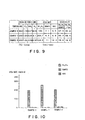
- the cleaning gas containing ammonia gas is capable of etching silicon nitride at a high etch rate and has high Si 3 N 4 selectivities with respect to quartz and SiC as shown in Figs. 9 and 11.
- the cleaning gas containing ammonia gas similarly to the cleaning gas containing chlorine gas, is capable of removing silicon nitride adhering to the inner surfaces of the reaction tube 2 without deteriorating the reaction tube 2 and the jigs.
- the cleaning gas into the inner tube 3 like Examples 6 to 8, such that the flow rate ratio between fluorine gas and ammonia gas is in the range of 2 : 1 and 10 : 1.
- Such a cleaning gas is capable of etching silicon nitride at a high etch rate.
- the cleaning gas supplied such that the flow rate ratio between fluorine gas and ammonia gas in carrying out Example 7 is about 4.5 : 1, can increases silicon nitride etch, and decrease quartz etch rate.
- silicon nitride selectivity with respect to quartz can be increased. Consequently, silicon nitride adhering to the inner surfaces of the reaction tube 2 can be removed without deteriorating the reaction tube 2 and the like.
- the cleaning gas containing hydrogen gas is capable of etching silicon nitride at a high etch rate and has high Si 3 N 4 selectivities with respect to quartz and SiC as shown in Figs. 12 and 14.
- the cleaning gas containing hydrogen gas similarly to the cleaning gas containing chlorine gas, is capable of removing silicon nitride adhering to the inner surfaces of the reaction tube 2 without deteriorating the reaction tube 2 and the jigs.
- the cleaning gas is supplied into the inner tube 3 like Examples 9 to 11, such that the flow rate ratio between fluorine gas and hydrogen gas is in the range of 5 : 1 and 5 : 3.
- a cleaning gas is capable of etching silicon nitride at a high etch rate. It was verified that the silicon nitride etching effect of the cleaning gas does not change significantly even if the flow rate ratio between fluorine gas and hydrogen gas changes in the range of 5 : 1 and 5 : 3. Therefore, high silicon nitride etch rate can be achieved even if the flow rate of hydrogen is not controlled precisely.
- the use of hydrogen gas as an additive gas can facilitate the control of the flow rate of the additive gas.
- Quartz etch rate does not increase even if the flow rate of hydrogen gas is increase so that the flow rate ratio between fluorine gas and hydrogen gas is 5 : 3 (Example 11). Consequently, the Si 3 N 4 selectivity with respect to quartz can further be increased and silicon nitride adhering to the inner surfaces of the reaction tube 2 can be removed without deteriorating the reaction tube 2 and the like.
- the cleaning gas containing the additive gas is capable of etching silicon nitride at a high etch rate without heating the reaction tube 2 at an elevated temperature. Since the Si 3 N 4 selectivity does not decrease when the cleaning gas containing the additive gas is used, and hence the reaction tube and the jigs are not deteriorated easily. Consequently, silicon nitride adhering to the inner surfaces of the thermal processing apparatus can be removed without deteriorating the reaction tube 2 and the jigs.
- the cleaning gas containing the additive gas is capable of etching silicon nitride at a high etch rate, and hence the reaction tube 2 may be heated at a comparatively low temperature for the cleaning step, which further reduces the deteriorating effect of the cleaning step on the reaction tube 2 and the jigs.
- the cleaning gas containing nitrogen gas as a diluent can facilitate setting a cleaning time for the cleaning process.
- the cleaning gas may contain any type of gas as an additive gas, provided that the additive gas is capable of promoting the activation of fluorine gas. Such a cleaning gas etches silicon nitride at a high etch rate.
- the cleaning gas may contain any type of additive gas, provided that the cleaning gas is capable of etching silicon nitride at a high etch rate without decreasing Si 3 N 4 selectivity with respect to materials forming the internal members of the thermal processing apparatus 1, such as quartz and SiC.
- the reaction tube 2 and the jigs are not deteriorated significantly when the cleaning gas has a high Si 3 N 4 selectivity.
- the additive gas may be a halogen gas, such as bromine gas (Br 2 ) instead of chlorine gas, hydrogen fluoride gas, ammonia gas or hydrogen gas.
- the present invention is applicable to removing deposits other than the silicon nitride deposit; the present invention can be applied to removing, for example, polysilicon, titanium oxide, tantalum oxide, silica, silicone-germanium (SiGe), BSTO (BaSrTiO 3 ) and STO (SrTiO 3 ).
- the deposit is not necessarily a reaction product, and may be a reaction byproduct, such as ammonium chloride.
- reaction product such as silicon nitride
- reaction byproduct such as ammonium chloride or a Si-Cl-N-H compound
- the cleaning gas is supplied through the reaction tube 2 into the exhaust pipe 17.
- the cleaning gas may be supplied through an inlet port 17a formed in the exhaust pipe 17 into the exhaust pipe 17.
- the deposits deposited on the inner surface of the exhaust pipe 17 can effectively removed by heating the exhaust pipe 17 with an exhaust pipe heater 17b.
- the cleaning gases do not necessarily need to contain the diluent gas.
- a cleaning gas containing a diluent gas because the cleaning gas containing the diluent gas facilitates setting a cleaning time for the cleaning process.
- the diluent gas is an inert gas.
- helium gas (He) neon gas (Ne) or argon gas (Ar) may be used instead of nitrogen gas.
- the pressure in the reaction tube 3 is not limited thereto.
- the cleaning of the thermal processing apparatus 1 may be carried out once every several cycles of the film deposition process or once every one cycle of the film deposition process.
- the life of the internal components formed of quartz and SiC of the thermal processing apparatus 1 can further be extended by cleaning the interior of the thermal processing apparatus once every one cycle of the film deposition process.
- the present invention is not limited thereto in its practical application.
- the present invention is applicable to cleaning a batch-furnace thermal processing apparatus provided with a reaction tube not having any tube corresponding to the inner tube 3.
- the workpieces are not limited to semiconductor wafers 10, and may be, for example, glass substrates for LCDs.
- the deposits deposited in the thermal processing apparatus can be removed without significantly deteriorating the reaction vessel and the jigs.
Landscapes
- Chemical & Material Sciences (AREA)
- General Chemical & Material Sciences (AREA)
- Chemical Kinetics & Catalysis (AREA)
- Engineering & Computer Science (AREA)
- Materials Engineering (AREA)
- Mechanical Engineering (AREA)
- Metallurgy (AREA)
- Organic Chemistry (AREA)
- Chemical Vapour Deposition (AREA)
- Drying Of Semiconductors (AREA)
Abstract
Description
Claims (22)
- A thin film deposition apparatus cleaning method of cleaning a thin film deposition apparatus by removing deposits adhering to an inner surfaces of the thin film deposition apparatus after depositing thin films on workpieces by supplying a process gas into a reaction vessel included in the thin film deposition apparatus, said thin film deposition apparatus cleaning method comprising the steps of:heating an interior of the reaction vessel at a predetermined temperature; andcleaning an interior of the thin film deposition apparatus by supplying a cleaning gas containing fluorine gas and an additive gas capable of promoting the activation of the fluorine gas into the reaction vessel heated at the predetermined temperature, heating the cleaning gas at a predetermined temperature to activate the fluorine gas contained in the cleaning gas, and removing the deposits with the activated fluorine gas.
- The thin film deposition apparatus cleaning method according to claim 1, wherein
the deposits are removed and the interior of the thin film deposition apparatus is cleaned by supplying the cleaning gas containing fluorine gas and the additive gas capable of promoting the activation of the fluorine gas and of increasing etch rate for the deposits without decreasing selectivity with respect to the materials forming the internal members of the thin film deposition apparatus, into the reaction vessel in the cleaning step. - The thin film deposition apparatus cleaning method according to claim 2, wherein
the additive gas is chlorine gas, hydrogen fluoride gas, ammonia gas or hydrogen gas. - The thin film deposition apparatus cleaning method according to claim 3, wherein
the deposits are removed to clean the interior of the thin film deposition apparatus by supplying a cleaning gas containing fluorine gas and chlorine gas into the reaction vessel heated at the predetermined temperature in the cleaning step. - The thin film deposition apparatus cleaning method according to claim 3, wherein
the deposits are removed to clean the interior of the thin film deposition apparatus by supplying a cleaning gas containing fluorine gas and hydrogen fluoride gas into the reaction vessel heated at a predetermined temperature in the cleaning step. - The thin film deposition apparatus cleaning method according to claim 3 or 5, wherein
the cleaning gas containing fluorine gas and hydrogen fluoride gas is supplied such that the flow rate ratio between fluorine gas and hydrogen fluoride gas is in the range of 1 : 3 to 3 : 1. - The thin film deposition apparatus cleaning method according to claim 6, wherein
the cleaning gas containing fluorine gas and hydrogen fluoride gas is supplied such that the flow rate ratio between fluorine gas and hydrogen fluoride gas is 1 : 1. - The thin film deposition apparatus cleaning method according to claim 7, wherein
fluorine gas and hydrogen fluoride gas are supplied at a flow rates not lower than 2 l/min respectively. - The thin film deposition apparatus cleaning method according to claim 3, wherein
the deposits are removed to clean the interior of the thin film deposition apparatus by supplying a cleaning gas containing fluorine gas and ammonia gas into the reaction vessel heated at a predetermined temperature in the cleaning step. - The thin film deposition apparatus cleaning method according to claim 9, wherein
the cleaning gas containing fluorine gas and ammonia gas is supplied such that the flow rate ratio between fluorine gas and ammonia gas is in the range of 2 : 1 to 10 : 1. - The thin film deposition apparatus cleaning method according to claim 3, wherein
the deposits are removed to clean the interior of the thin film deposition apparatus by supplying a cleaning gas containing fluorine gas and hydrogen gas into the reaction vessel heated at a predetermined temperature in the cleaning step. - The thin film deposition apparatus cleaning method according to claim 11, wherein
the cleaning gas containing fluorine gas and hydrogen gas is supplied such that the flow rate ratio between fluorine gas and hydrogen gas is in the range of 5 : 1 to 5 : 3. - The thin film deposition apparatus cleaning method according to claim 12, wherein
the cleaning gas containing fluorine gas and hydrogen gas is supplied such that the flow rate ratio between fluorine gas and hydrogen gas is 5 : 3. - The thin film deposition apparatus cleaning method according to claim 1, wherein
internal members of the thin film deposition apparatus are formed of at least either quartz or silicon carbide. - The thin film deposition apparatus cleaning method according to claim 1, wherein
the interior of the reaction vessel is heated at a temperature below 400°C in the heating step. - The thin film deposition apparatus cleaning method according to claim 15, wherein
the interior of the reaction vessel is heated at a temperature in the range of 250°C to 380°C in the heating step. - The thin film deposition apparatus cleaning method according to claim 1, wherein
the cleaning gas is diluted with a diluent gas to produce a diluted cleaning gas, and the diluted cleaning gas is supplied into the reaction vessel. - The thin film deposition apparatus cleaning method according to claim 17, wherein
the diluent gas is an inert gas. - The thin film deposition apparatus cleaning method according to claim 1, wherein
thin films formed on the workpieces are silicon nitride films, and
the silicon nitride deposited in the thin film deposition apparatus is removed in the cleaning step, when depositing the silicon nitride films on the workpieces with the cleaning gas. - A thin film deposition apparatus cleaning method of cleaning a thin film deposition apparatus by removing deposits adhering to the inner surface of an exhaust pipe after forming thin films on workpieces by supplying a process gas into a reaction vessel included in the thin film deposition apparatus, and discharging gases from the reaction vessel into the exhaust pipe, said thin film deposition apparatus cleaning method comprising the steps:heating an interior of the exhaust pipe at a predetermined temperature; andcleaning an interior of the exhaust pipe by supplying a cleaning gas containing fluorine gas, and an additive gas capable of promoting the activation of the fluorine gas into the exhaust pipe heated at the predetermined temperature in the heating step, heating the cleaning gas at a predetermined temperature to activate the fluorine gas contained in the cleaning gas, and removing the deposits with the activated fluorine gas.
- The thin film deposition apparatus cleaning method according to claim 20 wherein
the cleaning gas is supplied through the reaction vessel into the exhaust pipe. - The thin film deposition apparatus cleaning method according to claim 20, wherein
the cleaning gas is supplied through an inlet port formed in the exhaust pipe into the exhaust pipe.
Applications Claiming Priority (5)
| Application Number | Priority Date | Filing Date | Title |
|---|---|---|---|
| JP2001174129 | 2001-06-08 | ||
| JP2001174129 | 2001-06-08 | ||
| JP2001331590 | 2001-10-29 | ||
| JP2001331590A JP3421329B2 (en) | 2001-06-08 | 2001-10-29 | Cleaning method for thin film forming equipment |
| PCT/JP2002/001492 WO2002101805A1 (en) | 2001-06-08 | 2002-02-20 | Thin film forming apparatus cleaning method |
Publications (3)
| Publication Number | Publication Date |
|---|---|
| EP1394842A1 true EP1394842A1 (en) | 2004-03-03 |
| EP1394842A4 EP1394842A4 (en) | 2005-08-24 |
| EP1394842B1 EP1394842B1 (en) | 2008-08-27 |
Family
ID=26616617
Family Applications (1)
| Application Number | Title | Priority Date | Filing Date |
|---|---|---|---|
| EP02700635A Expired - Lifetime EP1394842B1 (en) | 2001-06-08 | 2002-02-20 | Thin film forming apparatus cleaning method |
Country Status (8)
| Country | Link |
|---|---|
| US (1) | US6925731B2 (en) |
| EP (1) | EP1394842B1 (en) |
| JP (1) | JP3421329B2 (en) |
| KR (2) | KR20070117005A (en) |
| CN (1) | CN1327485C (en) |
| DE (1) | DE60228568D1 (en) |
| TW (1) | TWI266811B (en) |
| WO (1) | WO2002101805A1 (en) |
Cited By (4)
| Publication number | Priority date | Publication date | Assignee | Title |
|---|---|---|---|---|
| EP1560252A3 (en) * | 2003-12-31 | 2006-03-29 | The Boc Group, Inc. | Deposition apparatus |
| WO2005104186A3 (en) * | 2004-03-25 | 2006-08-17 | Tokyo Electron Ltd | Method and processing system for plasma-enhanced cleaning of system components |
| EP1619269A3 (en) * | 2004-07-23 | 2006-11-08 | Air Products And Chemicals, Inc. | Method for enhancing fluorine utilization |
| EP1932941A1 (en) * | 2006-12-13 | 2008-06-18 | Air Products and Chemicals, Inc. | Thermal etch process for cleaning CVD chambers |
Families Citing this family (277)
| Publication number | Priority date | Publication date | Assignee | Title |
|---|---|---|---|---|
| JP4430918B2 (en) * | 2003-03-25 | 2010-03-10 | 東京エレクトロン株式会社 | Thin film forming apparatus cleaning method and thin film forming method |
| JP2004335789A (en) * | 2003-05-08 | 2004-11-25 | Tadahiro Omi | Cleaning method for substrate processing equipment |
| TWI389204B (en) * | 2003-09-19 | 2013-03-11 | 日立國際電氣股份有限公司 | Semiconductor device manufacturing method, substrate processing device, and substrate processing method |
| JP2005353958A (en) * | 2004-06-14 | 2005-12-22 | Hitachi Kokusai Electric Inc | Manufacturing method of semiconductor device |
| WO2006023894A2 (en) * | 2004-08-24 | 2006-03-02 | Saint-Gobain Ceramics & Plastics, Inc. | Semiconductor processing components and semiconductor processing utilizing same |
| JP4686157B2 (en) | 2004-09-29 | 2011-05-18 | 株式会社東芝 | Cleaning method for film forming apparatus |
| TWI365919B (en) * | 2004-12-28 | 2012-06-11 | Tokyo Electron Ltd | Film formation apparatus and method of using the same |
| JP4895256B2 (en) * | 2005-02-23 | 2012-03-14 | 東京エレクトロン株式会社 | Substrate surface treatment method |
| JP4703230B2 (en) * | 2005-03-29 | 2011-06-15 | 株式会社日立国際電気 | Semiconductor device manufacturing method and substrate processing apparatus |
| US7494943B2 (en) * | 2005-10-20 | 2009-02-24 | Tokyo Electron Limited | Method for using film formation apparatus |
| JP4786495B2 (en) * | 2005-11-24 | 2011-10-05 | 東京エレクトロン株式会社 | Thin film forming apparatus cleaning method, thin film forming method, thin film forming apparatus, and program |
| KR100706810B1 (en) * | 2006-02-07 | 2007-04-12 | 삼성전자주식회사 | Cleaning method of thin film forming apparatus and thin film forming method using same |
| JP4990594B2 (en) * | 2006-10-12 | 2012-08-01 | 東京エレクトロン株式会社 | Gas supply apparatus, gas supply method, thin film forming apparatus cleaning method, thin film forming method, and thin film forming apparatus |
| JP4919860B2 (en) * | 2007-03-30 | 2012-04-18 | 東京エレクトロン株式会社 | Gas analyzer and substrate processing apparatus |
| JP5213868B2 (en) * | 2007-09-19 | 2013-06-19 | 株式会社日立国際電気 | Cleaning method and substrate processing apparatus |
| JP4531833B2 (en) * | 2007-12-05 | 2010-08-25 | 株式会社日立国際電気 | Substrate processing apparatus, semiconductor device manufacturing method, and cleaning method |
| JP2009263764A (en) * | 2008-04-01 | 2009-11-12 | Hitachi Kokusai Electric Inc | Semiconductor manufacturing apparatus and semiconductor device manufacturing method |
| JP2010080850A (en) | 2008-09-29 | 2010-04-08 | Toshiba Corp | Semiconductor manufacturing device and cleaning method thereof |
| JP5210191B2 (en) * | 2009-02-03 | 2013-06-12 | 東京エレクトロン株式会社 | Silicon nitride film dry etching method |
| JP2009302555A (en) * | 2009-08-28 | 2009-12-24 | Toshiba Corp | Method of cleaning coating equipment |
| US8747762B2 (en) * | 2009-12-03 | 2014-06-10 | Applied Materials, Inc. | Methods and apparatus for treating exhaust gas in a processing system |
| JP5751895B2 (en) * | 2010-06-08 | 2015-07-22 | 株式会社日立国際電気 | Semiconductor device manufacturing method, cleaning method, and substrate processing apparatus |
| JP5524132B2 (en) * | 2010-07-15 | 2014-06-18 | 東京エレクトロン株式会社 | Thin film forming apparatus cleaning method, thin film forming method, and thin film forming apparatus |
| CN102174690A (en) * | 2011-01-13 | 2011-09-07 | 中国科学院苏州纳米技术与纳米仿生研究所 | MOCVD (metal-organic chemical vapor deposition) graphite disc cleaning device |
| JP5700538B2 (en) * | 2011-03-29 | 2015-04-15 | 東京エレクトロン株式会社 | Thin film forming apparatus cleaning method, thin film forming method, and thin film forming apparatus |
| CN102764745A (en) * | 2011-05-04 | 2012-11-07 | 青岛赛瑞达电子科技有限公司 | Baking furnace device of graphite disk for cleaning MOCVD (metal-organic chemical vapor deposition) device |
| US20130023129A1 (en) | 2011-07-20 | 2013-01-24 | Asm America, Inc. | Pressure transmitter for a semiconductor processing environment |
| JP5495449B2 (en) * | 2011-12-27 | 2014-05-21 | 株式会社日立国際電気 | Cleaning method, semiconductor device manufacturing method, and substrate processing apparatus |
| US20160376700A1 (en) | 2013-02-01 | 2016-12-29 | Asm Ip Holding B.V. | System for treatment of deposition reactor |
| US10724137B2 (en) * | 2013-02-05 | 2020-07-28 | Kokusai Eletric Corporation | Cleaning method, method of manufacturing semiconductor device, substrate processing apparatus, recording medium, and cleaning completion determining method |
| CN103234328B (en) * | 2013-03-28 | 2015-04-08 | 京东方科技集团股份有限公司 | Method for baseplate drying under reduced pressure and device thereof |
| JP2015073035A (en) * | 2013-10-03 | 2015-04-16 | 東京エレクトロン株式会社 | Etching method |
| US9962251B2 (en) | 2013-10-17 | 2018-05-08 | Boston Scientific Scimed, Inc. | Devices and methods for delivering implants |
| JP6349234B2 (en) * | 2014-02-19 | 2018-06-27 | 東京エレクトロン株式会社 | Silicon oxide film forming method and silicon oxide film forming apparatus |
| CN103938268B (en) * | 2014-04-03 | 2016-08-24 | 中国电子科技集团公司第五十五研究所 | A kind of method reducing silicon carbide epitaxial wafer surface particle density |
| US10858737B2 (en) | 2014-07-28 | 2020-12-08 | Asm Ip Holding B.V. | Showerhead assembly and components thereof |
| US10941490B2 (en) | 2014-10-07 | 2021-03-09 | Asm Ip Holding B.V. | Multiple temperature range susceptor, assembly, reactor and system including the susceptor, and methods of using the same |
| WO2016103924A1 (en) * | 2014-12-22 | 2016-06-30 | 昭和電工株式会社 | Method for cleaning silicon carbide deposits |
| US10276355B2 (en) | 2015-03-12 | 2019-04-30 | Asm Ip Holding B.V. | Multi-zone reactor, system including the reactor, and method of using the same |
| US11139308B2 (en) | 2015-12-29 | 2021-10-05 | Asm Ip Holding B.V. | Atomic layer deposition of III-V compounds to form V-NAND devices |
| US10529554B2 (en) | 2016-02-19 | 2020-01-07 | Asm Ip Holding B.V. | Method for forming silicon nitride film selectively on sidewalls or flat surfaces of trenches |
| US10343920B2 (en) | 2016-03-18 | 2019-07-09 | Asm Ip Holding B.V. | Aligned carbon nanotubes |
| US11453943B2 (en) | 2016-05-25 | 2022-09-27 | Asm Ip Holding B.V. | Method for forming carbon-containing silicon/metal oxide or nitride film by ALD using silicon precursor and hydrocarbon precursor |
| US9859151B1 (en) | 2016-07-08 | 2018-01-02 | Asm Ip Holding B.V. | Selective film deposition method to form air gaps |
| US10612137B2 (en) | 2016-07-08 | 2020-04-07 | Asm Ip Holdings B.V. | Organic reactants for atomic layer deposition |
| US9887082B1 (en) | 2016-07-28 | 2018-02-06 | Asm Ip Holding B.V. | Method and apparatus for filling a gap |
| US9812320B1 (en) | 2016-07-28 | 2017-11-07 | Asm Ip Holding B.V. | Method and apparatus for filling a gap |
| US11532757B2 (en) | 2016-10-27 | 2022-12-20 | Asm Ip Holding B.V. | Deposition of charge trapping layers |
| US10714350B2 (en) | 2016-11-01 | 2020-07-14 | ASM IP Holdings, B.V. | Methods for forming a transition metal niobium nitride film on a substrate by atomic layer deposition and related semiconductor device structures |
| KR102546317B1 (en) | 2016-11-15 | 2023-06-21 | 에이에스엠 아이피 홀딩 비.브이. | Gas supply unit and substrate processing apparatus including the same |
| US11581186B2 (en) | 2016-12-15 | 2023-02-14 | Asm Ip Holding B.V. | Sequential infiltration synthesis apparatus |
| US11447861B2 (en) | 2016-12-15 | 2022-09-20 | Asm Ip Holding B.V. | Sequential infiltration synthesis apparatus and a method of forming a patterned structure |
| US11390950B2 (en) | 2017-01-10 | 2022-07-19 | Asm Ip Holding B.V. | Reactor system and method to reduce residue buildup during a film deposition process |
| JP6767885B2 (en) * | 2017-01-18 | 2020-10-14 | 東京エレクトロン株式会社 | Protective film forming method |
| US10468261B2 (en) | 2017-02-15 | 2019-11-05 | Asm Ip Holding B.V. | Methods for forming a metallic film on a substrate by cyclical deposition and related semiconductor device structures |
| US10770286B2 (en) | 2017-05-08 | 2020-09-08 | Asm Ip Holdings B.V. | Methods for selectively forming a silicon nitride film on a substrate and related semiconductor device structures |
| US12040200B2 (en) | 2017-06-20 | 2024-07-16 | Asm Ip Holding B.V. | Semiconductor processing apparatus and methods for calibrating a semiconductor processing apparatus |
| US11306395B2 (en) | 2017-06-28 | 2022-04-19 | Asm Ip Holding B.V. | Methods for depositing a transition metal nitride film on a substrate by atomic layer deposition and related deposition apparatus |
| KR20190009245A (en) | 2017-07-18 | 2019-01-28 | 에이에스엠 아이피 홀딩 비.브이. | Methods for forming a semiconductor device structure and related semiconductor device structures |
| US11374112B2 (en) | 2017-07-19 | 2022-06-28 | Asm Ip Holding B.V. | Method for depositing a group IV semiconductor and related semiconductor device structures |
| US10590535B2 (en) | 2017-07-26 | 2020-03-17 | Asm Ip Holdings B.V. | Chemical treatment, deposition and/or infiltration apparatus and method for using the same |
| TWI815813B (en) | 2017-08-04 | 2023-09-21 | 荷蘭商Asm智慧財產控股公司 | Showerhead assembly for distributing a gas within a reaction chamber |
| US10770336B2 (en) | 2017-08-08 | 2020-09-08 | Asm Ip Holding B.V. | Substrate lift mechanism and reactor including same |
| US10692741B2 (en) | 2017-08-08 | 2020-06-23 | Asm Ip Holdings B.V. | Radiation shield |
| US11769682B2 (en) | 2017-08-09 | 2023-09-26 | Asm Ip Holding B.V. | Storage apparatus for storing cassettes for substrates and processing apparatus equipped therewith |
| US11830730B2 (en) | 2017-08-29 | 2023-11-28 | Asm Ip Holding B.V. | Layer forming method and apparatus |
| US11295980B2 (en) | 2017-08-30 | 2022-04-05 | Asm Ip Holding B.V. | Methods for depositing a molybdenum metal film over a dielectric surface of a substrate by a cyclical deposition process and related semiconductor device structures |
| US10658205B2 (en) | 2017-09-28 | 2020-05-19 | Asm Ip Holdings B.V. | Chemical dispensing apparatus and methods for dispensing a chemical to a reaction chamber |
| US10403504B2 (en) | 2017-10-05 | 2019-09-03 | Asm Ip Holding B.V. | Method for selectively depositing a metallic film on a substrate |
| US10923344B2 (en) | 2017-10-30 | 2021-02-16 | Asm Ip Holding B.V. | Methods for forming a semiconductor structure and related semiconductor structures |
| JP7214724B2 (en) | 2017-11-27 | 2023-01-30 | エーエスエム アイピー ホールディング ビー.ブイ. | Storage device for storing wafer cassettes used in batch furnaces |
| TWI791689B (en) | 2017-11-27 | 2023-02-11 | 荷蘭商Asm智慧財產控股私人有限公司 | Apparatus including a clean mini environment |
| US10872771B2 (en) | 2018-01-16 | 2020-12-22 | Asm Ip Holding B. V. | Method for depositing a material film on a substrate within a reaction chamber by a cyclical deposition process and related device structures |
| TWI799494B (en) | 2018-01-19 | 2023-04-21 | 荷蘭商Asm 智慧財產控股公司 | Deposition method |
| KR102695659B1 (en) | 2018-01-19 | 2024-08-14 | 에이에스엠 아이피 홀딩 비.브이. | Method for depositing a gap filling layer by plasma assisted deposition |
| US11081345B2 (en) | 2018-02-06 | 2021-08-03 | Asm Ip Holding B.V. | Method of post-deposition treatment for silicon oxide film |
| US11685991B2 (en) | 2018-02-14 | 2023-06-27 | Asm Ip Holding B.V. | Method for depositing a ruthenium-containing film on a substrate by a cyclical deposition process |
| US10896820B2 (en) | 2018-02-14 | 2021-01-19 | Asm Ip Holding B.V. | Method for depositing a ruthenium-containing film on a substrate by a cyclical deposition process |
| US10731249B2 (en) | 2018-02-15 | 2020-08-04 | Asm Ip Holding B.V. | Method of forming a transition metal containing film on a substrate by a cyclical deposition process, a method for supplying a transition metal halide compound to a reaction chamber, and related vapor deposition apparatus |
| KR102636427B1 (en) | 2018-02-20 | 2024-02-13 | 에이에스엠 아이피 홀딩 비.브이. | Substrate processing method and apparatus |
| JP6785809B2 (en) * | 2018-02-22 | 2020-11-18 | 株式会社Kokusai Electric | Methods for cleaning members in processing vessels, methods for manufacturing semiconductor devices, substrate processing devices, and programs |
| US10975470B2 (en) | 2018-02-23 | 2021-04-13 | Asm Ip Holding B.V. | Apparatus for detecting or monitoring for a chemical precursor in a high temperature environment |
| US11473195B2 (en) | 2018-03-01 | 2022-10-18 | Asm Ip Holding B.V. | Semiconductor processing apparatus and a method for processing a substrate |
| KR102646467B1 (en) | 2018-03-27 | 2024-03-11 | 에이에스엠 아이피 홀딩 비.브이. | Method of forming an electrode on a substrate and a semiconductor device structure including an electrode |
| KR102600229B1 (en) | 2018-04-09 | 2023-11-10 | 에이에스엠 아이피 홀딩 비.브이. | Substrate supporting device, substrate processing apparatus including the same and substrate processing method |
| US12025484B2 (en) | 2018-05-08 | 2024-07-02 | Asm Ip Holding B.V. | Thin film forming method |
| US12272527B2 (en) | 2018-05-09 | 2025-04-08 | Asm Ip Holding B.V. | Apparatus for use with hydrogen radicals and method of using same |
| KR102596988B1 (en) | 2018-05-28 | 2023-10-31 | 에이에스엠 아이피 홀딩 비.브이. | Method of processing a substrate and a device manufactured by the same |
| US11718913B2 (en) | 2018-06-04 | 2023-08-08 | Asm Ip Holding B.V. | Gas distribution system and reactor system including same |
| KR102568797B1 (en) | 2018-06-21 | 2023-08-21 | 에이에스엠 아이피 홀딩 비.브이. | Substrate processing system |
| US10797133B2 (en) | 2018-06-21 | 2020-10-06 | Asm Ip Holding B.V. | Method for depositing a phosphorus doped silicon arsenide film and related semiconductor device structures |
| US11499222B2 (en) | 2018-06-27 | 2022-11-15 | Asm Ip Holding B.V. | Cyclic deposition methods for forming metal-containing material and films and structures including the metal-containing material |
| TWI871083B (en) | 2018-06-27 | 2025-01-21 | 荷蘭商Asm Ip私人控股有限公司 | Cyclic deposition processes for forming metal-containing material |
| US10755922B2 (en) | 2018-07-03 | 2020-08-25 | Asm Ip Holding B.V. | Method for depositing silicon-free carbon-containing film as gap-fill layer by pulse plasma-assisted deposition |
| US10388513B1 (en) | 2018-07-03 | 2019-08-20 | Asm Ip Holding B.V. | Method for depositing silicon-free carbon-containing film as gap-fill layer by pulse plasma-assisted deposition |
| US11053591B2 (en) | 2018-08-06 | 2021-07-06 | Asm Ip Holding B.V. | Multi-port gas injection system and reactor system including same |
| US11430674B2 (en) | 2018-08-22 | 2022-08-30 | Asm Ip Holding B.V. | Sensor array, apparatus for dispensing a vapor phase reactant to a reaction chamber and related methods |
| KR102707956B1 (en) | 2018-09-11 | 2024-09-19 | 에이에스엠 아이피 홀딩 비.브이. | Method for deposition of a thin film |
| US11024523B2 (en) | 2018-09-11 | 2021-06-01 | Asm Ip Holding B.V. | Substrate processing apparatus and method |
| CN110970344B (en) | 2018-10-01 | 2024-10-25 | Asmip控股有限公司 | Substrate holding device, system including the same and method of using the same |
| KR102592699B1 (en) | 2018-10-08 | 2023-10-23 | 에이에스엠 아이피 홀딩 비.브이. | Substrate support unit and apparatuses for depositing thin film and processing the substrate including the same |
| KR102546322B1 (en) | 2018-10-19 | 2023-06-21 | 에이에스엠 아이피 홀딩 비.브이. | Substrate processing apparatus and substrate processing method |
| US12378665B2 (en) | 2018-10-26 | 2025-08-05 | Asm Ip Holding B.V. | High temperature coatings for a preclean and etch apparatus and related methods |
| US11087997B2 (en) | 2018-10-31 | 2021-08-10 | Asm Ip Holding B.V. | Substrate processing apparatus for processing substrates |
| KR102748291B1 (en) | 2018-11-02 | 2024-12-31 | 에이에스엠 아이피 홀딩 비.브이. | Substrate support unit and substrate processing apparatus including the same |
| US11572620B2 (en) | 2018-11-06 | 2023-02-07 | Asm Ip Holding B.V. | Methods for selectively depositing an amorphous silicon film on a substrate |
| US10818758B2 (en) | 2018-11-16 | 2020-10-27 | Asm Ip Holding B.V. | Methods for forming a metal silicate film on a substrate in a reaction chamber and related semiconductor device structures |
| US12040199B2 (en) | 2018-11-28 | 2024-07-16 | Asm Ip Holding B.V. | Substrate processing apparatus for processing substrates |
| US11217444B2 (en) | 2018-11-30 | 2022-01-04 | Asm Ip Holding B.V. | Method for forming an ultraviolet radiation responsive metal oxide-containing film |
| KR102636428B1 (en) | 2018-12-04 | 2024-02-13 | 에이에스엠 아이피 홀딩 비.브이. | A method for cleaning a substrate processing apparatus |
| US11158513B2 (en) | 2018-12-13 | 2021-10-26 | Asm Ip Holding B.V. | Methods for forming a rhenium-containing film on a substrate by a cyclical deposition process and related semiconductor device structures |
| JP7504584B2 (en) | 2018-12-14 | 2024-06-24 | エーエスエム・アイピー・ホールディング・ベー・フェー | Method and system for forming device structures using selective deposition of gallium nitride - Patents.com |
| TWI866480B (en) | 2019-01-17 | 2024-12-11 | 荷蘭商Asm Ip 私人控股有限公司 | Methods of forming a transition metal containing film on a substrate by a cyclical deposition process |
| JP7190915B2 (en) * | 2019-01-18 | 2022-12-16 | 東京エレクトロン株式会社 | Substrate processing apparatus cleaning method and substrate processing apparatus |
| TWI845607B (en) | 2019-02-20 | 2024-06-21 | 荷蘭商Asm Ip私人控股有限公司 | Cyclical deposition method and apparatus for filling a recess formed within a substrate surface |
| TWI873122B (en) | 2019-02-20 | 2025-02-21 | 荷蘭商Asm Ip私人控股有限公司 | Method of filling a recess formed within a surface of a substrate, semiconductor structure formed according to the method, and semiconductor processing apparatus |
| KR20200102357A (en) | 2019-02-20 | 2020-08-31 | 에이에스엠 아이피 홀딩 비.브이. | Apparatus and methods for plug fill deposition in 3-d nand applications |
| TWI842826B (en) | 2019-02-22 | 2024-05-21 | 荷蘭商Asm Ip私人控股有限公司 | Substrate processing apparatus and method for processing substrate |
| KR102858005B1 (en) | 2019-03-08 | 2025-09-09 | 에이에스엠 아이피 홀딩 비.브이. | Method for Selective Deposition of Silicon Nitride Layer and Structure Including Selectively-Deposited Silicon Nitride Layer |
| KR102762833B1 (en) | 2019-03-08 | 2025-02-04 | 에이에스엠 아이피 홀딩 비.브이. | STRUCTURE INCLUDING SiOCN LAYER AND METHOD OF FORMING SAME |
| JP2020167398A (en) | 2019-03-28 | 2020-10-08 | エーエスエム・アイピー・ホールディング・ベー・フェー | Door openers and substrate processing equipment provided with door openers |
| KR102809999B1 (en) | 2019-04-01 | 2025-05-19 | 에이에스엠 아이피 홀딩 비.브이. | Method of manufacturing semiconductor device |
| KR102897355B1 (en) | 2019-04-19 | 2025-12-08 | 에이에스엠 아이피 홀딩 비.브이. | Layer forming method and apparatus |
| KR20200125453A (en) | 2019-04-24 | 2020-11-04 | 에이에스엠 아이피 홀딩 비.브이. | Gas-phase reactor system and method of using same |
| KR102929471B1 (en) | 2019-05-07 | 2026-02-20 | 에이에스엠 아이피 홀딩 비.브이. | Chemical source vessel with dip tube |
| KR102929472B1 (en) | 2019-05-10 | 2026-02-20 | 에이에스엠 아이피 홀딩 비.브이. | Method of depositing material onto a surface and structure formed according to the method |
| JP7612342B2 (en) | 2019-05-16 | 2025-01-14 | エーエスエム・アイピー・ホールディング・ベー・フェー | Wafer boat handling apparatus, vertical batch furnace and method |
| JP7598201B2 (en) | 2019-05-16 | 2024-12-11 | エーエスエム・アイピー・ホールディング・ベー・フェー | Wafer boat handling apparatus, vertical batch furnace and method |
| USD947913S1 (en) | 2019-05-17 | 2022-04-05 | Asm Ip Holding B.V. | Susceptor shaft |
| USD975665S1 (en) | 2019-05-17 | 2023-01-17 | Asm Ip Holding B.V. | Susceptor shaft |
| KR20200141002A (en) | 2019-06-06 | 2020-12-17 | 에이에스엠 아이피 홀딩 비.브이. | Method of using a gas-phase reactor system including analyzing exhausted gas |
| KR102918757B1 (en) | 2019-06-10 | 2026-01-28 | 에이에스엠 아이피 홀딩 비.브이. | Method for cleaning quartz epitaxial chambers |
| KR20200143254A (en) | 2019-06-11 | 2020-12-23 | 에이에스엠 아이피 홀딩 비.브이. | Method of forming an electronic structure using an reforming gas, system for performing the method, and structure formed using the method |
| KR102911421B1 (en) | 2019-07-03 | 2026-01-12 | 에이에스엠 아이피 홀딩 비.브이. | Temperature control assembly for substrate processing apparatus and method of using same |
| JP7499079B2 (en) | 2019-07-09 | 2024-06-13 | エーエスエム・アイピー・ホールディング・ベー・フェー | Plasma device using coaxial waveguide and substrate processing method |
| CN112216646B (en) | 2019-07-10 | 2026-02-10 | Asmip私人控股有限公司 | Substrate support assembly and substrate processing apparatus including the thereof |
| KR102895115B1 (en) | 2019-07-16 | 2025-12-03 | 에이에스엠 아이피 홀딩 비.브이. | Substrate processing apparatus |
| TWI826704B (en) | 2019-07-17 | 2023-12-21 | 荷蘭商Asm Ip私人控股有限公司 | Radical assist ignition plasma system and method |
| KR102860110B1 (en) | 2019-07-17 | 2025-09-16 | 에이에스엠 아이피 홀딩 비.브이. | Methods of forming silicon germanium structures |
| US11643724B2 (en) | 2019-07-18 | 2023-05-09 | Asm Ip Holding B.V. | Method of forming structures using a neutral beam |
| KR102903090B1 (en) | 2019-07-19 | 2025-12-19 | 에이에스엠 아이피 홀딩 비.브이. | Method of Forming Topology-Controlled Amorphous Carbon Polymer Film |
| CN112309843B (en) | 2019-07-29 | 2026-01-23 | Asmip私人控股有限公司 | Selective deposition method for achieving high dopant incorporation |
| KR20210015655A (en) | 2019-07-30 | 2021-02-10 | 에이에스엠 아이피 홀딩 비.브이. | Substrate processing apparatus and method |
| CN112309899B (en) | 2019-07-30 | 2025-11-14 | Asmip私人控股有限公司 | Substrate processing equipment |
| CN112309900B (en) | 2019-07-30 | 2025-11-04 | Asmip私人控股有限公司 | Substrate processing equipment |
| US11587814B2 (en) | 2019-07-31 | 2023-02-21 | Asm Ip Holding B.V. | Vertical batch furnace assembly |
| US11587815B2 (en) | 2019-07-31 | 2023-02-21 | Asm Ip Holding B.V. | Vertical batch furnace assembly |
| US11227782B2 (en) | 2019-07-31 | 2022-01-18 | Asm Ip Holding B.V. | Vertical batch furnace assembly |
| KR20210018759A (en) | 2019-08-05 | 2021-02-18 | 에이에스엠 아이피 홀딩 비.브이. | Liquid level sensor for a chemical source vessel |
| KR20210018761A (en) | 2019-08-09 | 2021-02-18 | 에이에스엠 아이피 홀딩 비.브이. | heater assembly including cooling apparatus and method of using same |
| USD965044S1 (en) | 2019-08-19 | 2022-09-27 | Asm Ip Holding B.V. | Susceptor shaft |
| USD965524S1 (en) | 2019-08-19 | 2022-10-04 | Asm Ip Holding B.V. | Susceptor support |
| JP7810514B2 (en) | 2019-08-21 | 2026-02-03 | エーエスエム・アイピー・ホールディング・ベー・フェー | Film-forming raw material mixed gas generating device and film-forming device |
| KR20210024423A (en) | 2019-08-22 | 2021-03-05 | 에이에스엠 아이피 홀딩 비.브이. | Method for forming a structure with a hole |
| USD979506S1 (en) | 2019-08-22 | 2023-02-28 | Asm Ip Holding B.V. | Insulator |
| US11286558B2 (en) | 2019-08-23 | 2022-03-29 | Asm Ip Holding B.V. | Methods for depositing a molybdenum nitride film on a surface of a substrate by a cyclical deposition process and related semiconductor device structures including a molybdenum nitride film |
| KR102928101B1 (en) | 2019-08-23 | 2026-02-13 | 에이에스엠 아이피 홀딩 비.브이. | Method for depositing silicon oxide film having improved quality by peald using bis(diethylamino)silane |
| KR102868968B1 (en) | 2019-09-03 | 2025-10-10 | 에이에스엠 아이피 홀딩 비.브이. | Methods and apparatus for depositing a chalcogenide film and structures including the film |
| KR102806450B1 (en) | 2019-09-04 | 2025-05-12 | 에이에스엠 아이피 홀딩 비.브이. | Methods for selective deposition using a sacrificial capping layer |
| KR102733104B1 (en) | 2019-09-05 | 2024-11-22 | 에이에스엠 아이피 홀딩 비.브이. | Substrate processing apparatus |
| US12469693B2 (en) | 2019-09-17 | 2025-11-11 | Asm Ip Holding B.V. | Method of forming a carbon-containing layer and structure including the layer |
| JP7026086B2 (en) | 2019-09-25 | 2022-02-25 | 株式会社Kokusai Electric | Substrate processing equipment, semiconductor device manufacturing method, and substrate processing equipment cleaning method |
| US11562901B2 (en) | 2019-09-25 | 2023-01-24 | Asm Ip Holding B.V. | Substrate processing method |
| CN112593212B (en) | 2019-10-02 | 2023-12-22 | Asm Ip私人控股有限公司 | Method for forming topologically selective silicon oxide film through cyclic plasma enhanced deposition process |
| TWI846953B (en) | 2019-10-08 | 2024-07-01 | 荷蘭商Asm Ip私人控股有限公司 | Substrate processing device |
| TW202128273A (en) | 2019-10-08 | 2021-08-01 | 荷蘭商Asm Ip私人控股有限公司 | Gas injection system, reactor system, and method of depositing material on surface of substratewithin reaction chamber |
| KR102948143B1 (en) | 2019-10-08 | 2026-04-07 | 에이에스엠 아이피 홀딩 비.브이. | Reactor system including a gas distribution assembly for use with activated species and method of using same |
| TWI846966B (en) | 2019-10-10 | 2024-07-01 | 荷蘭商Asm Ip私人控股有限公司 | Method of forming a photoresist underlayer and structure including same |
| US12009241B2 (en) | 2019-10-14 | 2024-06-11 | Asm Ip Holding B.V. | Vertical batch furnace assembly with detector to detect cassette |
| TWI834919B (en) | 2019-10-16 | 2024-03-11 | 荷蘭商Asm Ip私人控股有限公司 | Method of topology-selective film formation of silicon oxide |
| US11637014B2 (en) | 2019-10-17 | 2023-04-25 | Asm Ip Holding B.V. | Methods for selective deposition of doped semiconductor material |
| KR102845724B1 (en) | 2019-10-21 | 2025-08-13 | 에이에스엠 아이피 홀딩 비.브이. | Apparatus and methods for selectively etching films |
| US11996292B2 (en) | 2019-10-25 | 2024-05-28 | Asm Ip Holding B.V. | Methods for filling a gap feature on a substrate surface and related semiconductor structures |
| US11646205B2 (en) | 2019-10-29 | 2023-05-09 | Asm Ip Holding B.V. | Methods of selectively forming n-type doped material on a surface, systems for selectively forming n-type doped material, and structures formed using same |
| KR102890638B1 (en) | 2019-11-05 | 2025-11-25 | 에이에스엠 아이피 홀딩 비.브이. | Structures with doped semiconductor layers and methods and systems for forming same |
| US11501968B2 (en) | 2019-11-15 | 2022-11-15 | Asm Ip Holding B.V. | Method for providing a semiconductor device with silicon filled gaps |
| KR102861314B1 (en) | 2019-11-20 | 2025-09-17 | 에이에스엠 아이피 홀딩 비.브이. | Method of depositing carbon-containing material on a surface of a substrate, structure formed using the method, and system for forming the structure |
| CN112951697B (en) | 2019-11-26 | 2025-07-29 | Asmip私人控股有限公司 | Substrate processing apparatus |
| KR20210065848A (en) | 2019-11-26 | 2021-06-04 | 에이에스엠 아이피 홀딩 비.브이. | Methods for selectivley forming a target film on a substrate comprising a first dielectric surface and a second metallic surface |
| CN112885692B (en) | 2019-11-29 | 2025-08-15 | Asmip私人控股有限公司 | Substrate processing apparatus |
| CN120432376A (en) | 2019-11-29 | 2025-08-05 | Asm Ip私人控股有限公司 | Substrate processing equipment |
| JP7527928B2 (en) | 2019-12-02 | 2024-08-05 | エーエスエム・アイピー・ホールディング・ベー・フェー | Substrate processing apparatus and substrate processing method |
| KR20210070898A (en) | 2019-12-04 | 2021-06-15 | 에이에스엠 아이피 홀딩 비.브이. | Substrate processing apparatus |
| US11885013B2 (en) | 2019-12-17 | 2024-01-30 | Asm Ip Holding B.V. | Method of forming vanadium nitride layer and structure including the vanadium nitride layer |
| KR102943768B1 (en) | 2019-12-19 | 2026-03-26 | 에이에스엠 아이피 홀딩 비.브이. | Methods for filling a gap feature on a substrate and related semiconductor structures |
| TWI887322B (en) | 2020-01-06 | 2025-06-21 | 荷蘭商Asm Ip私人控股有限公司 | Reactor system, lift pin, and processing method |
| JP7730637B2 (en) | 2020-01-06 | 2025-08-28 | エーエスエム・アイピー・ホールディング・ベー・フェー | Gas delivery assembly, components thereof, and reactor system including same |
| US11993847B2 (en) | 2020-01-08 | 2024-05-28 | Asm Ip Holding B.V. | Injector |
| KR102882467B1 (en) | 2020-01-16 | 2025-11-05 | 에이에스엠 아이피 홀딩 비.브이. | Method of forming high aspect ratio features |
| KR102675856B1 (en) | 2020-01-20 | 2024-06-17 | 에이에스엠 아이피 홀딩 비.브이. | Method of forming thin film and method of modifying surface of thin film |
| TWI889744B (en) | 2020-01-29 | 2025-07-11 | 荷蘭商Asm Ip私人控股有限公司 | Contaminant trap system, and baffle plate stack |
| TW202513845A (en) | 2020-02-03 | 2025-04-01 | 荷蘭商Asm Ip私人控股有限公司 | Semiconductor structures and methods for forming the same |
| KR20210100010A (en) | 2020-02-04 | 2021-08-13 | 에이에스엠 아이피 홀딩 비.브이. | Method and apparatus for transmittance measurements of large articles |
| US11776846B2 (en) | 2020-02-07 | 2023-10-03 | Asm Ip Holding B.V. | Methods for depositing gap filling fluids and related systems and devices |
| KR102916725B1 (en) | 2020-02-13 | 2026-01-23 | 에이에스엠 아이피 홀딩 비.브이. | Substrate processing apparatus including light receiving device and calibration method of light receiving device |
| KR20210103953A (en) | 2020-02-13 | 2021-08-24 | 에이에스엠 아이피 홀딩 비.브이. | Gas distribution assembly and method of using same |
| US11781243B2 (en) | 2020-02-17 | 2023-10-10 | Asm Ip Holding B.V. | Method for depositing low temperature phosphorous-doped silicon |
| TWI895326B (en) | 2020-02-28 | 2025-09-01 | 荷蘭商Asm Ip私人控股有限公司 | System dedicated for parts cleaning |
| KR102943116B1 (en) | 2020-03-04 | 2026-03-23 | 에이에스엠 아이피 홀딩 비.브이. | Alignment fixture for a reactor system |
| KR20210116240A (en) | 2020-03-11 | 2021-09-27 | 에이에스엠 아이피 홀딩 비.브이. | Substrate handling device with adjustable joints |
| US11876356B2 (en) | 2020-03-11 | 2024-01-16 | Asm Ip Holding B.V. | Lockout tagout assembly and system and method of using same |
| KR102775390B1 (en) | 2020-03-12 | 2025-02-28 | 에이에스엠 아이피 홀딩 비.브이. | Method for Fabricating Layer Structure Having Target Topological Profile |
| US12173404B2 (en) | 2020-03-17 | 2024-12-24 | Asm Ip Holding B.V. | Method of depositing epitaxial material, structure formed using the method, and system for performing the method |
| KR102755229B1 (en) | 2020-04-02 | 2025-01-14 | 에이에스엠 아이피 홀딩 비.브이. | Thin film forming method |
| TWI887376B (en) | 2020-04-03 | 2025-06-21 | 荷蘭商Asm Ip私人控股有限公司 | Method for manufacturing semiconductor device |
| TWI888525B (en) | 2020-04-08 | 2025-07-01 | 荷蘭商Asm Ip私人控股有限公司 | Apparatus and methods for selectively etching silcon oxide films |
| KR20210127620A (en) | 2020-04-13 | 2021-10-22 | 에이에스엠 아이피 홀딩 비.브이. | method of forming a nitrogen-containing carbon film and system for performing the method |
| US11821078B2 (en) | 2020-04-15 | 2023-11-21 | Asm Ip Holding B.V. | Method for forming precoat film and method for forming silicon-containing film |
| KR20210128343A (en) | 2020-04-15 | 2021-10-26 | 에이에스엠 아이피 홀딩 비.브이. | Method of forming chromium nitride layer and structure including the chromium nitride layer |
| US11996289B2 (en) | 2020-04-16 | 2024-05-28 | Asm Ip Holding B.V. | Methods of forming structures including silicon germanium and silicon layers, devices formed using the methods, and systems for performing the methods |
| KR102901748B1 (en) | 2020-04-21 | 2025-12-17 | 에이에스엠 아이피 홀딩 비.브이. | Method for processing a substrate |
| TW202539998A (en) | 2020-04-24 | 2025-10-16 | 荷蘭商Asm Ip私人控股有限公司 | Compositions and vessels including vanadium compounds, and methods and systems for stabilizing vanadium compounds |
| CN113555279A (en) | 2020-04-24 | 2021-10-26 | Asm Ip私人控股有限公司 | Methods of forming vanadium nitride-containing layers and structures comprising the same |
| KR102866804B1 (en) | 2020-04-24 | 2025-09-30 | 에이에스엠 아이피 홀딩 비.브이. | Vertical batch furnace assembly comprising a cooling gas supply |
| KR20210132600A (en) | 2020-04-24 | 2021-11-04 | 에이에스엠 아이피 홀딩 비.브이. | Methods and systems for depositing a layer comprising vanadium, nitrogen, and a further element |
| KR102934380B1 (en) | 2020-04-24 | 2026-03-05 | 에이에스엠 아이피 홀딩 비.브이. | Methods of forming structures including vanadium boride and vanadium phosphide layers |
| KR102783898B1 (en) | 2020-04-29 | 2025-03-18 | 에이에스엠 아이피 홀딩 비.브이. | Solid source precursor vessel |
| KR20210134869A (en) | 2020-05-01 | 2021-11-11 | 에이에스엠 아이피 홀딩 비.브이. | Fast FOUP swapping with a FOUP handler |
| JP7726664B2 (en) | 2020-05-04 | 2025-08-20 | エーエスエム・アイピー・ホールディング・ベー・フェー | Substrate processing system for processing a substrate |
| KR20210137395A (en) | 2020-05-07 | 2021-11-17 | 에이에스엠 아이피 홀딩 비.브이. | Apparatus and methods for performing an in-situ etch of reaction chambers with fluorine-based radicals |
| JP7736446B2 (en) | 2020-05-07 | 2025-09-09 | エーエスエム・アイピー・ホールディング・ベー・フェー | Reactor system with tuned circuit |
| KR102788543B1 (en) | 2020-05-13 | 2025-03-27 | 에이에스엠 아이피 홀딩 비.브이. | Laser alignment fixture for a reactor system |
| KR102936676B1 (en) | 2020-05-15 | 2026-03-10 | 에이에스엠 아이피 홀딩 비.브이. | Methods for silicon germanium uniformity control using multiple precursors |
| KR102905441B1 (en) | 2020-05-19 | 2025-12-30 | 에이에스엠 아이피 홀딩 비.브이. | Substrate processing apparatus |
| KR20210145079A (en) | 2020-05-21 | 2021-12-01 | 에이에스엠 아이피 홀딩 비.브이. | Flange and apparatus for processing substrates |
| KR102795476B1 (en) | 2020-05-21 | 2025-04-11 | 에이에스엠 아이피 홀딩 비.브이. | Structures including multiple carbon layers and methods of forming and using same |
| TWI873343B (en) | 2020-05-22 | 2025-02-21 | 荷蘭商Asm Ip私人控股有限公司 | Reaction system for forming thin film on substrate |
| KR20210146802A (en) | 2020-05-26 | 2021-12-06 | 에이에스엠 아이피 홀딩 비.브이. | Method for depositing boron and gallium containing silicon germanium layers |
| TWI876048B (en) | 2020-05-29 | 2025-03-11 | 荷蘭商Asm Ip私人控股有限公司 | Substrate processing device |
| TW202212620A (en) | 2020-06-02 | 2022-04-01 | 荷蘭商Asm Ip私人控股有限公司 | Apparatus for processing substrate, method of forming film, and method of controlling apparatus for processing substrate |
| KR20210156219A (en) | 2020-06-16 | 2021-12-24 | 에이에스엠 아이피 홀딩 비.브이. | Method for depositing boron containing silicon germanium layers |
| TWI908816B (en) | 2020-06-24 | 2025-12-21 | 荷蘭商Asm Ip私人控股有限公司 | Method for forming a layer provided with silicon |
| TWI873359B (en) | 2020-06-30 | 2025-02-21 | 荷蘭商Asm Ip私人控股有限公司 | Substrate processing method |
| KR102707957B1 (en) | 2020-07-08 | 2024-09-19 | 에이에스엠 아이피 홀딩 비.브이. | Method for processing a substrate |
| KR20220010438A (en) | 2020-07-17 | 2022-01-25 | 에이에스엠 아이피 홀딩 비.브이. | Structures and methods for use in photolithography |
| TWI878570B (en) | 2020-07-20 | 2025-04-01 | 荷蘭商Asm Ip私人控股有限公司 | Method and system for depositing molybdenum layers |
| KR20220011092A (en) | 2020-07-20 | 2022-01-27 | 에이에스엠 아이피 홀딩 비.브이. | Method and system for forming structures including transition metal layers |
| TW202219303A (en) | 2020-07-27 | 2022-05-16 | 荷蘭商Asm Ip私人控股有限公司 | Thin film deposition process |
| KR20220020210A (en) | 2020-08-11 | 2022-02-18 | 에이에스엠 아이피 홀딩 비.브이. | Methods for Depositing a Titinum Aluminun Carbide Film Structuru on a Substrate and Releated Semiconductor Structures |
| KR102915124B1 (en) | 2020-08-14 | 2026-01-19 | 에이에스엠 아이피 홀딩 비.브이. | Method for processing a substrate |
| US12040177B2 (en) | 2020-08-18 | 2024-07-16 | Asm Ip Holding B.V. | Methods for forming a laminate film by cyclical plasma-enhanced deposition processes |
| TWI911263B (en) | 2020-08-25 | 2026-01-11 | 荷蘭商Asm Ip私人控股有限公司 | Method for cleaning a substrate, method for selectively depositing, and reaction system |
| TW202534193A (en) | 2020-08-26 | 2025-09-01 | 荷蘭商Asm Ip私人控股有限公司 | Method of forming metal silicon oxide layer and metal silicon oxynitride layer |
| TWI911265B (en) | 2020-08-27 | 2026-01-11 | 荷蘭商Asm Ip私人控股有限公司 | Method of forming patterned structures, method of manipulating mechanical property, and device structure |
| USD990534S1 (en) | 2020-09-11 | 2023-06-27 | Asm Ip Holding B.V. | Weighted lift pin |
| KR20220036866A (en) | 2020-09-16 | 2022-03-23 | 에이에스엠 아이피 홀딩 비.브이. | Silicon oxide deposition method |
| USD1012873S1 (en) | 2020-09-24 | 2024-01-30 | Asm Ip Holding B.V. | Electrode for semiconductor processing apparatus |
| TWI889903B (en) | 2020-09-25 | 2025-07-11 | 荷蘭商Asm Ip私人控股有限公司 | Semiconductor processing method |
| US12009224B2 (en) | 2020-09-29 | 2024-06-11 | Asm Ip Holding B.V. | Apparatus and method for etching metal nitrides |
| TW202229612A (en) | 2020-10-06 | 2022-08-01 | 荷蘭商Asm Ip私人控股有限公司 | Method and system for forming silicon nitride on a sidewall of a feature |
| KR20220045900A (en) | 2020-10-06 | 2022-04-13 | 에이에스엠 아이피 홀딩 비.브이. | Deposition method and an apparatus for depositing a silicon-containing material |
| CN114293174A (en) | 2020-10-07 | 2022-04-08 | Asm Ip私人控股有限公司 | Gas supply unit and substrate processing apparatus including the same |
| KR102855834B1 (en) | 2020-10-14 | 2025-09-04 | 에이에스엠 아이피 홀딩 비.브이. | Method of Depositing Material on Stepped Structure |
| KR102873665B1 (en) | 2020-10-15 | 2025-10-17 | 에이에스엠 아이피 홀딩 비.브이. | Method of manufacturing semiconductor device, and substrate treatment apparatus using ether-cat |
| TW202217037A (en) | 2020-10-22 | 2022-05-01 | 荷蘭商Asm Ip私人控股有限公司 | Method of depositing vanadium metal, structure, device and a deposition assembly |
| TW202223136A (en) | 2020-10-28 | 2022-06-16 | 荷蘭商Asm Ip私人控股有限公司 | Method for forming layer on substrate, and semiconductor processing system |
| TW202229620A (en) | 2020-11-12 | 2022-08-01 | 特文特大學 | Deposition system, method for controlling reaction condition, method for depositing |
| WO2022109009A1 (en) * | 2020-11-20 | 2022-05-27 | Applied Materials, Inc. | Cleaning materials and processes for lithium processing equipment |
| TW202229795A (en) | 2020-11-23 | 2022-08-01 | 荷蘭商Asm Ip私人控股有限公司 | A substrate processing apparatus with an injector |
| TW202235649A (en) | 2020-11-24 | 2022-09-16 | 荷蘭商Asm Ip私人控股有限公司 | Methods for filling a gap and related systems and devices |
| TW202235675A (en) | 2020-11-30 | 2022-09-16 | 荷蘭商Asm Ip私人控股有限公司 | Injector, and substrate processing apparatus |
| KR20220077875A (en) | 2020-12-02 | 2022-06-09 | 에이에스엠 아이피 홀딩 비.브이. | Cleaning fixture for showerhead assemblies |
| US12255053B2 (en) | 2020-12-10 | 2025-03-18 | Asm Ip Holding B.V. | Methods and systems for depositing a layer |
| US12159788B2 (en) | 2020-12-14 | 2024-12-03 | Asm Ip Holding B.V. | Method of forming structures for threshold voltage control |
| CN114639631A (en) | 2020-12-16 | 2022-06-17 | Asm Ip私人控股有限公司 | Fixing device for measuring jumping and swinging |
| TW202232639A (en) | 2020-12-18 | 2022-08-16 | 荷蘭商Asm Ip私人控股有限公司 | Wafer processing apparatus with a rotatable table |
| TW202226899A (en) | 2020-12-22 | 2022-07-01 | 荷蘭商Asm Ip私人控股有限公司 | Plasma treatment device having matching box |
| KR20220090435A (en) | 2020-12-22 | 2022-06-29 | 에이에스엠 아이피 홀딩 비.브이. | Precursor capsule, vessel and method |
| KR20220090438A (en) | 2020-12-22 | 2022-06-29 | 에이에스엠 아이피 홀딩 비.브이. | Transition metal deposition method |
| JP7638700B2 (en) * | 2020-12-24 | 2025-03-04 | 東京エレクトロン株式会社 | SUBSTRATE PROCESSING METHOD AND SUBSTRATE PROCESSING APPARATUS |
| USD1023959S1 (en) | 2021-05-11 | 2024-04-23 | Asm Ip Holding B.V. | Electrode for substrate processing apparatus |
| USD980814S1 (en) | 2021-05-11 | 2023-03-14 | Asm Ip Holding B.V. | Gas distributor for substrate processing apparatus |
| USD980813S1 (en) | 2021-05-11 | 2023-03-14 | Asm Ip Holding B.V. | Gas flow control plate for substrate processing apparatus |
| USD981973S1 (en) | 2021-05-11 | 2023-03-28 | Asm Ip Holding B.V. | Reactor wall for substrate processing apparatus |
| USD990441S1 (en) | 2021-09-07 | 2023-06-27 | Asm Ip Holding B.V. | Gas flow control plate |
| USD1099184S1 (en) | 2021-11-29 | 2025-10-21 | Asm Ip Holding B.V. | Weighted lift pin |
| USD1060598S1 (en) | 2021-12-03 | 2025-02-04 | Asm Ip Holding B.V. | Split showerhead cover |
Family Cites Families (16)
| Publication number | Priority date | Publication date | Assignee | Title |
|---|---|---|---|---|
| US4872938A (en) * | 1987-07-16 | 1989-10-10 | Texas Instruments Incorporated | Processing apparatus |
| JP2746448B2 (en) * | 1990-02-07 | 1998-05-06 | セントラル硝子株式会社 | Mixed gas composition |
| GB9011535D0 (en) * | 1990-05-23 | 1990-07-11 | Oxford Lasers Ltd | Gas management system |
| JPH0496222A (en) | 1990-08-03 | 1992-03-27 | Fujitsu Ltd | Manufacture of semiconductor device |
| US5609721A (en) * | 1994-03-11 | 1997-03-11 | Fujitsu Limited | Semiconductor device manufacturing apparatus and its cleaning method |
| US5966623A (en) * | 1995-10-25 | 1999-10-12 | Eastman Kodak Company | Metal impurity neutralization within semiconductors by fluorination |
| JPH1072672A (en) * | 1996-07-09 | 1998-03-17 | Applied Materials Inc | Non-plasma chamber cleaning method |
| US6030932A (en) * | 1996-09-06 | 2000-02-29 | Olin Microelectronic Chemicals | Cleaning composition and method for removing residues |
| JP3594759B2 (en) * | 1997-03-19 | 2004-12-02 | 株式会社日立製作所 | Plasma processing method |
| US6383300B1 (en) * | 1998-11-27 | 2002-05-07 | Tokyo Electron Ltd. | Heat treatment apparatus and cleaning method of the same |
| JP2000265276A (en) | 1999-01-12 | 2000-09-26 | Central Glass Co Ltd | Cleaning gas |
| US6374831B1 (en) | 1999-02-04 | 2002-04-23 | Applied Materials, Inc. | Accelerated plasma clean |
| JP3456933B2 (en) * | 1999-12-28 | 2003-10-14 | 株式会社東芝 | Semiconductor processing apparatus cleaning method and semiconductor processing apparatus |
| JP2001267241A (en) * | 2000-03-10 | 2001-09-28 | L'air Liquide | Method and apparatus for cleaning, and method and apparatus for etching |
| US20030010354A1 (en) | 2000-03-27 | 2003-01-16 | Applied Materials, Inc. | Fluorine process for cleaning semiconductor process chamber |
| DE10029523A1 (en) * | 2000-06-21 | 2002-01-10 | Messer Griesheim Gmbh | Method and device for cleaning a PVD or CVD reactor and exhaust pipes of the same |
-
2001
- 2001-10-29 JP JP2001331590A patent/JP3421329B2/en not_active Expired - Lifetime
-
2002
- 2002-02-20 WO PCT/JP2002/001492 patent/WO2002101805A1/en not_active Ceased
- 2002-02-20 CN CNB028155122A patent/CN1327485C/en not_active Expired - Lifetime
- 2002-02-20 US US10/479,718 patent/US6925731B2/en not_active Expired - Lifetime
- 2002-02-20 EP EP02700635A patent/EP1394842B1/en not_active Expired - Lifetime
- 2002-02-20 DE DE60228568T patent/DE60228568D1/en not_active Expired - Lifetime
- 2002-02-20 KR KR1020077027864A patent/KR20070117005A/en not_active Ceased
- 2002-02-20 KR KR1020037015945A patent/KR100825135B1/en not_active Expired - Lifetime
- 2002-03-08 TW TW091104642A patent/TWI266811B/en not_active IP Right Cessation
Cited By (4)
| Publication number | Priority date | Publication date | Assignee | Title |
|---|---|---|---|---|
| EP1560252A3 (en) * | 2003-12-31 | 2006-03-29 | The Boc Group, Inc. | Deposition apparatus |
| WO2005104186A3 (en) * | 2004-03-25 | 2006-08-17 | Tokyo Electron Ltd | Method and processing system for plasma-enhanced cleaning of system components |
| EP1619269A3 (en) * | 2004-07-23 | 2006-11-08 | Air Products And Chemicals, Inc. | Method for enhancing fluorine utilization |
| EP1932941A1 (en) * | 2006-12-13 | 2008-06-18 | Air Products and Chemicals, Inc. | Thermal etch process for cleaning CVD chambers |
Also Published As
| Publication number | Publication date |
|---|---|
| WO2002101805A1 (en) | 2002-12-19 |
| DE60228568D1 (en) | 2008-10-09 |
| JP2003059915A (en) | 2003-02-28 |
| EP1394842A4 (en) | 2005-08-24 |
| EP1394842B1 (en) | 2008-08-27 |
| KR20070117005A (en) | 2007-12-11 |
| JP3421329B2 (en) | 2003-06-30 |
| US20050090123A1 (en) | 2005-04-28 |
| CN1327485C (en) | 2007-07-18 |
| US6925731B2 (en) | 2005-08-09 |
| KR20040008212A (en) | 2004-01-28 |
| KR100825135B1 (en) | 2008-04-24 |
| TWI266811B (en) | 2006-11-21 |
| CN1539159A (en) | 2004-10-20 |
Similar Documents
| Publication | Publication Date | Title |
|---|---|---|
| US6925731B2 (en) | Thin film forming apparatus cleaning method | |
| US6844273B2 (en) | Precleaning method of precleaning a silicon nitride film forming system | |
| US7713354B2 (en) | Film forming method, film forming system and recording medium | |
| TWI435385B (en) | Film forming device and method using same | |
| WO2004086482A1 (en) | Method for cleaning thin-film forming apparatus | |
| TWI895405B (en) | Etching method and etching apparatus | |
| KR20180016308A (en) | Aluminum fluoride mitigation by plasma treatment | |
| US7520937B2 (en) | Thin film forming apparatus and method of cleaning the same | |
| US20060081182A1 (en) | Method of cleaning thin film deposition system, thin film deposition system and program | |
| JP4675127B2 (en) | Thin film forming apparatus, thin film forming apparatus cleaning method and program | |
| US20090253269A1 (en) | Semiconductor manufacturing apparatus and semiconductor device manufacturing method | |
| EP1167568B1 (en) | Heat treatment apparatus and cleaning method of the same | |
| EP1724374A1 (en) | Method and process for reactive gas cleaning of tool parts | |
| CN1322558C (en) | Cleaning method of substrate treating apparatus, and substrate treating apparatus | |
| JP2003347288A (en) | Injector for semiconductor manufacturing apparatus, semiconductor manufacturing apparatus, and method of cleaning semiconductor manufacturing apparatus | |
| US20020020433A1 (en) | Oxidation apparatus and method of cleaning the same | |
| JP3581890B2 (en) | Heat treatment method and heat treatment apparatus | |
| JP2004288903A (en) | Method for manufacturing semiconductor device | |
| JP4325473B2 (en) | Cleaning method for heat treatment apparatus | |
| WO2004095555A1 (en) | Method for cleaning heat treatment apparatus | |
| JP2024062579A (en) | SUBSTRATE PROCESSING METHOD AND SUBSTRATE PROCESSING APPARATUS | |
| JP2005079123A (en) | Method for cleaning film forming apparatus | |
| JP5661444B2 (en) | Thin film forming apparatus, thin film forming apparatus cleaning method and program | |
| JP2025158811A (en) | Film forming apparatus operating method and film forming apparatus | |
| JP2006108595A (en) | Manufacturing method of semiconductor device |
Legal Events
| Date | Code | Title | Description |
|---|---|---|---|
| PUAI | Public reference made under article 153(3) epc to a published international application that has entered the european phase |
Free format text: ORIGINAL CODE: 0009012 |
|
| 17P | Request for examination filed |
Effective date: 20031204 |
|
| AK | Designated contracting states |
Kind code of ref document: A1 Designated state(s): AT BE CH CY DE DK ES FI FR GB GR IE IT LI LU MC NL PT SE TR |
|
| RIN1 | Information on inventor provided before grant (corrected) |
Inventor name: SPAULL, PHILLIP Inventor name: NISHIMURA, KAZUAKI Inventor name: TAGO, KENJI Inventor name: TOJO, YUKIO |
|
| A4 | Supplementary search report drawn up and despatched |
Effective date: 20050711 |
|
| GRAP | Despatch of communication of intention to grant a patent |
Free format text: ORIGINAL CODE: EPIDOSNIGR1 |
|
| GRAS | Grant fee paid |
Free format text: ORIGINAL CODE: EPIDOSNIGR3 |
|
| GRAA | (expected) grant |
Free format text: ORIGINAL CODE: 0009210 |
|
| AK | Designated contracting states |
Kind code of ref document: B1 Designated state(s): DE FR GB IT NL |
|
| REG | Reference to a national code |
Ref country code: GB Ref legal event code: FG4D |
|
| REF | Corresponds to: |
Ref document number: 60228568 Country of ref document: DE Date of ref document: 20081009 Kind code of ref document: P |
|
| PLBE | No opposition filed within time limit |
Free format text: ORIGINAL CODE: 0009261 |
|
| STAA | Information on the status of an ep patent application or granted ep patent |
Free format text: STATUS: NO OPPOSITION FILED WITHIN TIME LIMIT |
|
| 26N | No opposition filed |
Effective date: 20090528 |
|
| REG | Reference to a national code |
Ref country code: FR Ref legal event code: PLFP Year of fee payment: 15 |
|
| PGFP | Annual fee paid to national office [announced via postgrant information from national office to epo] |
Ref country code: NL Payment date: 20160111 Year of fee payment: 15 |
|
| PGFP | Annual fee paid to national office [announced via postgrant information from national office to epo] |
Ref country code: IT Payment date: 20160222 Year of fee payment: 15 Ref country code: DE Payment date: 20160216 Year of fee payment: 15 |
|
| PGFP | Annual fee paid to national office [announced via postgrant information from national office to epo] |
Ref country code: GB Payment date: 20160217 Year of fee payment: 15 |
|
| REG | Reference to a national code |
Ref country code: FR Ref legal event code: PLFP Year of fee payment: 16 |
|
| PGFP | Annual fee paid to national office [announced via postgrant information from national office to epo] |
Ref country code: FR Payment date: 20170112 Year of fee payment: 16 |
|
| REG | Reference to a national code |
Ref country code: DE Ref legal event code: R119 Ref document number: 60228568 Country of ref document: DE |
|
| REG | Reference to a national code |
Ref country code: NL Ref legal event code: MM Effective date: 20170301 |
|
| GBPC | Gb: european patent ceased through non-payment of renewal fee |
Effective date: 20170220 |
|
| PG25 | Lapsed in a contracting state [announced via postgrant information from national office to epo] |
Ref country code: NL Free format text: LAPSE BECAUSE OF NON-PAYMENT OF DUE FEES Effective date: 20170301 |
|
| PG25 | Lapsed in a contracting state [announced via postgrant information from national office to epo] |
Ref country code: DE Free format text: LAPSE BECAUSE OF NON-PAYMENT OF DUE FEES Effective date: 20170901 |
|
| PG25 | Lapsed in a contracting state [announced via postgrant information from national office to epo] |
Ref country code: IT Free format text: LAPSE BECAUSE OF NON-PAYMENT OF DUE FEES Effective date: 20170220 Ref country code: GB Free format text: LAPSE BECAUSE OF NON-PAYMENT OF DUE FEES Effective date: 20170220 |
|
| REG | Reference to a national code |
Ref country code: FR Ref legal event code: ST Effective date: 20181031 |
|
| PG25 | Lapsed in a contracting state [announced via postgrant information from national office to epo] |
Ref country code: FR Free format text: LAPSE BECAUSE OF NON-PAYMENT OF DUE FEES Effective date: 20180228 |