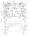
BACKGROUND OF THE INVENTION
Field of the Invention
The present invention relates to a motor control circuit
for a mirror device used in an electric door mirror device or the
like for a vehicle.
Description of the Related Art
Among rearview door mirrors disposed at the side of a door
panel in correspondence with a driver seat or a passenger seat
in a vehicle, there is an electric door mirror device where the
door mirror can be folded and stored by the driving force of a
motor so that the mirror faces a substantial vehicle width
direction interior.
This type of electric door mirror device is ordinarily
disposed with a folding/deploying switch disposed near the driver
seat in the vehicle. Power is supplied from the battery of the
vehicle to a folding/deploying motor via the switch and a control
circuit of the motor (see Japanese Patent Application Laid-Open
(JP-A) No. 8-142756).
In the electric door mirror device, the control circuit is
configured to stop the motor when the mirror has been rotated to
a fixed deployed position and a fixed folded position. As an
example of such a control circuit, there is a configuration that
detects a load applied to the motor and cuts off current flowing
to the motor when a load of a predetermined value or greater has
been applied to the motor.
That is, the mirror is rotated to the deployed position or
the folded position and further rotation thereof is restricted.
Thus, when the motor is locked, a lock current that is larger than
an ordinary activation current flows to the motor. The control
circuit has a configuration that cuts off the current flowing to
the motor when the lock current has flowed to the motor.
Although a relay circuit is used for the control circuit
of the configuration that detects the lock current and cuts off
the current flowing to the motor, a relay circuit usually has
drawbacks in that the circuit scale is large and the circuit
configuration is complicated.
SUMMARY OF THE INVENTION
In light of the above-described facts, it is an object of
the present invention to obtain a mirror device motor control
circuit that can reliably stop a mirror at predetermined
positions with a simple configuration.
The present invention is a control circuit that is used in
a mirror device, where the position of a mirror attached to a
vehicle is changed in a predetermined direction by the driving
force of a motor, and controls electrical power supplied to the
motor, the control circuit comprising: a drive current
controlling transistor where, when a first terminal is connected
to a power source, a second terminal is connected to the motor
and a voltage equal to or greater than a predetermined value is
applied to a third terminal that is different from both the first
and second terminals, a current flows from the first terminal to
the second terminal and application of the voltage is released,
whereby the current is blocked; and a switching transistor where
a fourth terminal is connected between the power source and the
third terminal, a fifth terminal is grounded, and which includes
a sixth terminal connected to the motor at an opposite side from
the second terminal, and a voltage equal to or greater than a
specific value corresponding to a lock current flowing through
the motor is applied to the sixth terminal, whereby the fourth
terminal and the fifth terminal are switched to a conductive state
and the voltage applied to the third terminal is made less than
the predetermined value.
In the mirror device mirror control circuit of the
above-described configuration, the drive current controlling
transistor is intervened between the motor and the power source.
The voltage equal to or greater than the predetermined value is
applied to the third terminal of the drive current controlling
transistor, whereby between the first terminal and the second
terminal is placed in a conductive state, the current flows to
the motor, and the motor is driven. The position of the mirror
is changed by the driving force of the motor. For example, if
the motor is a motor for storing and deploying the mirror, the
position of the mirror is changed by the driving force of the motor
from a storage position to a deployed position or from the
deployed position to the storage position.
Also, as described above, the motor is driven and the
position of the mirror is changed to the deployed position or the
storage position so that, when further change in the position of
the mirror is regulated by a stopper or the like, an output shaft
of the motor is not rotated even if the drive current flows to
the motor. Thus, the lock current flows to the motor and the value
of the current flowing to the motor rises.
The sixth terminal of the switching transistor is connected
at the opposite side from the second terminal of the motor, and
the voltage corresponding to the current flowing through the
motor is applied to the sixth terminal. Here, as described above,
when the lock current flows and the voltage applied to the sixth
terminal becomes equal to or greater than the predetermined value,
the fourth terminal and the fifth terminal of the switching
transistor are placed in a conductive state.
The fourth terminal of the switching terminal is connected
between the power source and the third terminal of the drive
current controlling transistor, and the fifth terminal is
grounded. For this reason, when the fourth terminal and the fifth
terminal of the switching transistor are placed in a conductive
state, part or all of the current that had flowed to the third
terminal is grounded via the fourth terminal and the fifth
terminal of the switching transistor, and the voltage applied to
the third terminal becomes less than the predetermined value.
Thus, the drive current controlling transistor is switched to an
OFF state and the current with respect to the motor is cut off.
In this manner, the present invention has a configuration
that stops the motor on the basis of the lock current flowing to
the motor. For this reason, miniaturization becomes possible
with a simple configuration and costs are also lowered in
comparison with a configuration that uses a relay circuit to cut
off the current flowing to the motor at a position at which the
motor is locked.
Moreover, the invention has a configuration that stops the
motor on the basis of the lock current flowing to the motor. For
this reason, when the invention is used to control a motor that
stores and deploys a mirror, the invention can be applied to
mirrors whose amount of displacement from the storage position
to the deployed position differs, without having to fundamentally
change the design of the circuit.
It should be noted that, in the present invention, the drive
current controlling transistor and the switching transistor may
be transistors of any configuration, including field-effect
transistors. Also, in the present invention, the respective
terminals in the drive current controlling transistor and the
switching transistor are called first to sixth terminals. This
is because, whereas the terminals are called base terminals,
collector terminals and emitter terminals in common transistors,
the terminals are called drain terminals, gate terminals and
source terminals in field-effect transistors. In the present
invention, the first to sixth terminals are not limited to
terminals having such specific names.
The invention may also be disposed with a waveform
conversion component that converts the waveform of the voltage
applied to the sixth terminal, lowers a maximum value of an output
voltage lower than a maximum value of a substantially pulse-like
voltage equal to or greater than the inputted specific value, and
inputs the maximum value to the sixth terminal.
In the mirror device motor control circuit of the
above-described configuration, when the extemporaneous
substantially pulse-like current such as an inrush current flows
to the circuit immediately after activation of the motor has
started, the voltage resulting from this current is applied to
the sixth terminal of the switching transistor. However, in the
present invention, this voltage is not directly applied to the
sixth terminal; rather, the waveform of the voltage is converted
by the waveform conversion component before it is applied to the
sixth terminal.
Due to this conversion of the waveform, the voltage is
lowered to less than the specific value-i.e., less than the value
of the current necessary to make the fourth terminal and the fifth
terminal conductive-and is outputted. Thus, a voltage equal to
or greater than the predetermined value-i.e., equal to or greater
than the value of the current necessary to make the first terminal
and the second terminal conductive-can be applied to the third
terminal of the drive current controlling transistor at the time,
or immediately after, driving of the motor is initiated.
The invention may also be disposed with a compensation
component that lowers, in accompaniment with the elapse of time,
the voltage equal to or greater than the predetermined value on
the basis of a current corresponding to the pulse-like voltage
in a state where the pulse-like voltage equal to or greater than
the specific value is applied to the sixth terminal.
In the mirror device motor control circuit of the
above-described configuration, when the extemporaneous
substantially pulse-like current such as an inrush current flows
to the circuit immediately after activation of the motor has
started, the voltage resulting from this current is applied to
the sixth terminal of the switching transistor.
Thus, as long as this voltage is equal to or greater than
the specific value, the fourth terminal and the fifth terminal
of the switching transistor become conductive and the value of
the current applied to the third terminal of the drive current
controlling transistor falls below the predetermined value.
Here, in the present invention, as described above, when
the extemporaneous substantially pulse-like current flows to the
circuit, the compensation component applies the voltage
corresponding to this substantially pulse-like current to the
third terminal of the drive current controlling transistor. For
this reason, the extemporaneous substantially pulse-like current
flows to the circuit and conduction between the first terminal
and the second terminal of the drive current controlling
transistor during the time when the fourth terminal and the fifth
terminal of the switching transistor are conductive can be
secured. Thus, the motor can be reliably driven.
Because the compensation component applies the voltage to
the third terminal while lowering the voltage in accompaniment
with the elapse of time, the voltage that the compensation
component applied to the third terminal falls below the
predetermined value after a set period of time has elapsed, even
if application of the voltage corresponding to the third terminal
by the compensation component is initiated. For this reason, a
voltage equal to or greater than the predetermined value can be
prevented from being applied to the third terminal over a long
period of time in a state where the fourth terminal and the fifth
terminal of the switching transistor are conductive.
The invention may also be disposed with a bypass component
where a voltage corresponding to the pulse-like current equal to
or greater than the specific value is lowered in accompaniment
with the elapse of time and applied, is switched to an ON state
and grounds the pulse-like current proceeding to the third
terminal before transmitting the pulse-like current to the third
terminal.
In the mirror device motor control circuit of the
above-described configuration, when the extemporaneous
substantially pulse-like current such as an inrush current flows
to the circuit immediately after activation of the motor has
started, the voltage resulting from this current is applied to
the sixth terminal of the switching transistor.
Thus, as long as this voltage is equal to or greater than
the specific value, the fourth terminal and the fifth terminal
of the switching transistor become conductive and the value of
the current applied to the third terminal of the drive current
controlling transistor falls below the predetermined value.
Here, in the present invention, as described above, when
the extemporaneous substantially pulse-like current flows to the
circuit, the voltage corresponding to this current is applied to
the bypass component, whereby the bypass component is switched
to the ON state. In the ON state of the bypass component, the
current proceeding to the sixth terminal of the switching
transistor is grounded before it reaches the sixth terminal. For
this reason, even if the extemporaneous substantially pulse-like
current flows, the motor can be reliably started without the
fourth terminal and the fifth terminal of the switching
transistor becoming conductive.
Moreover, because the voltage applied to the bypass
component is lowered in accompaniment with the elapse of time,
the bypass component is switched to the OFF state after the set
period of time has elapsed. Thus, the voltage corresponding to
the lock current can be applied to the sixth terminal.
The invention may also be disposed with a storage element
that stores a charge due to the current flowing to the third
terminal and reduces the current flowing to the third terminal
in accordance with the amount of the stored charge.
In the mirror device motor control circuit of the
above-described configuration, when the current equal to or
greater than the predetermined value flows to the third terminal
of the drive current controlling transistor, a charge is stored
in the storage element connected to the third terminal. Moreover,
when the charge stored in the storage element increases due to
the current continuing to flow to the third terminal, the current
flowing to the third terminal is reduced in accordance with the
amount of the charge that the storage element has stored. Thus,
eventually the voltage applied to the third terminal falls below
the predetermined value, conduction between the first terminal
and the second terminal is released, the drive current flowing
to the motor is cut off, and the motor is stopped.
Here, the amount of the charge that the storage element
stores during the period of time from when between the first
terminal and the second terminal is placed in a conductive state
to until the conduction is released is dependent on the time when
the third terminal is placed in a conductive state. For this
reason, the motor is fundamentally driven only for a set period
of time from when the first terminal and the second terminal have
been placed in a conductive state, and the position of the mirror
is changed only by a set amount.
In this manner, in the present invention, because the motor
is not driven for a period of time equal to or greater than the
set period of time, the motor can be reliably stopped, even if
the voltage equal to or greater than the specific value is not
applied to the sixth terminal of the switching transistor in the
event that an amount of time equal to or greater than the set
period of time has elapsed.
As described above, the mirror device motor control circuit
pertaining to the invention can miniaturize a configuration with
a simple configuration and can reliably stop a mirror at
predetermined positions.
BRIEF DESCRIPTION OF THE DRAWINGS
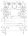
Fig. 1 is a circuit diagram of a mirror device motor control
circuit pertaining to a first embodiment of the present
invention;
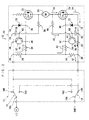
Fig. 2 is a circuit diagram corresponding to Fig. 1 in a
state where a lock current is flowing;
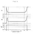
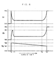
Fig. 3 is a time chart showing waveforms of voltages applied
to each of a third terminal of a drive current controlling
transistor and a sixth terminal of a switching transistor;
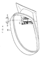
Fig. 4 is a perspective view of a mirror device;
Fig. 5 is a circuit diagram of a mirror device motor control
circuit pertaining to a second embodiment of the present
invention;
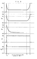
Fig. 6 is a time chart showing waveforms of voltages applied
to each of a third terminal of a drive current controlling
transistor and a sixth terminal of a switching transistor;
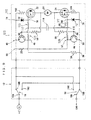
Fig. 7 is a circuit diagram of a mirror device motor control
circuit pertaining to a third embodiment of the present
invention;
Fig. 8 is a time chart showing waveforms of voltages applied
to each of a third terminal of a drive current controlling
transistor and a sixth terminal of a switching transistor;
Fig. 9 is a circuit diagram of a mirror device motor control
circuit pertaining to a fourth embodiment of the present
invention;
Fig. 10 is a circuit diagram of a mirror device motor
control circuit pertaining to a fifth embodiment of the present
invention;
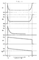
Fig. 11 is a time chart showing waveforms of voltages
applied to each of a third terminal of a drive current controlling
transistor and a sixth terminal of a switching transistor; and
Fig. 12 is a circuit diagram of a mirror device motor
control circuit pertaining to a sixth embodiment of the present
invention.
DETAILED DESCRIPTION OF THE INVENTION
Configuration of First Embodiment
In Fig. 1, the configuration of a mirror device motor
control circuit 10 (referred to below simply as "the control
circuit 10") pertaining to a first embodiment of the invention
is illustrated by a circuit diagram.
As illustrated in this diagram, the present control circuit
10 is disposed with a switch section 12 and a drive control section
14. The switch section 12 is disposed with a pair of switches
16 and 18. The switch 16 is disposed with three terminals 16A,
16B and 16C, and is configured so that one of between the terminal
16A and the terminal 16B and between the terminal 16A and the
terminal 16C is placed in a conductive state and the other is
placed in a disconnected state.
The switch 18 is similarly disposed with three terminals
18A, 18B and 18C, and is configured so that one of between the
terminal 18A and the terminal 18B and between the terminal 18A
and the terminal 18C is placed in a conductive state and the other
is placed in a disconnected state. However, whereas the terminal
16A of the switch 16 is connected to the positive terminal of a
battery installed in the vehicle, the terminal 18A of the switch
18 is grounded. Also, in the switches 16 and 18, the terminal
16B is connected to the terminal 18C and the terminal 16C is
connected to the terminal 18B.
Moreover, the switches 16 and 18 are set so as mutually
interwork. When the terminal 16A and the terminal 16B are
connected by the switch 16, the terminal 18A and the terminal 18B
are connected by the switch 18, and when the terminal 16A and the
terminal 16C are connected by the switch 16, the terminal 18A and
the terminal 18C are connected by the switch 18.
The drive control section 14 is disposed with a motor 20
and a pair of n-channel field-effect transistors 22 and 24
(referred to below simply as "the MOSFETs 22 and 24") respectively
serving as drive current controlling transistors. The motor 20
is housed at an inner side of a door mirror 26 serving as the mirror
shown in Fig. 4. An output shaft is directly or indirectly and
mechanically connected to a support shaft 27 that rotatably
supports, using the substantial vertical direction of the vehicle
as an axial direction, the door mirror 26 around this axis. Due
to the output shaft rotating, the door mirror 26 is rotated in
a deployment direction (the direction of arrow Y1 in Fig. 4) or
a storage direction (the direction of arrow Y2 in Fig. 4).
One terminal of the motor 20 is connected to a drain
terminal serving as a second terminal of the MOSFET 22. In the
MOSFET 22, a source terminal serving as a first terminal is
connected to the terminal 16B of the switch 16 and to the terminal
18C of the switch 18. With respect thereto, the other terminal
of the motor 20 is connected to a drain terminal serving as a
second terminal of the MOSFET 24. In the MOSFET 24, a source
terminal serving as a first terminal is connected to the terminal
16C of the switch 16 and to the terminal 18B of the switch 18.
The drive control section 14 is also disposed with a
resistor 28. One end of the resistor 28 is connected to a contact
point 30 between the terminal 16B of the switch 16 and the terminal
18C of the switch 18 and the source terminal of the MOSFET 22.
The other end of the resistor 28 is connected to an end of a
resistor 34. Moreover, the other end of the resistor 34 is
connected to a contact point 36 between the source terminal of
the MOSFET 24 and the terminal 18B of the switch 18 and the
terminal 16C of the switch 16.
The other end of the resistor 28 is also connected to a
terminal of a resistor 38. The other end of the resistor 38 is
connected to a gate terminal serving as a third terminal of the
MOSFET 22. Moreover, the other end of the resistor 28 is connected
to an end of a resistor 40 between the other end of the resistor
28 and the end of the resistor 34. The other end of the resistor
40 is connected to a gate terminal serving as a third terminal
of the MOSFET 24.
Moreover, the drive control section 14 is disposed with a
pair of NPN transistors 42 and 44 respectively serving as
switching transistors. In the transistor 42, an emitter terminal
serving as a fifth terminal is connected to a contact point 46
between the contact point 30 and the source terminal of the MOSFET
22, and a collector terminal serving as a fourth terminal is
connected to a contact point 48 between the resistor 38 and the
gate terminal of the MOSFET 22. In the transistor 44, an emitter
terminal serving as a fifth terminal is connected to a contact
point 50 between the contact point 36 and the source terminal of
the MOSFET 24, and a collector terminal serving as a fourth
terminal is connected to a contact point 52 between the resistor
40 and the gate terminal of the MOSFET 24.
An end of a capacitor 56 configuring a waveform conversion
component is connected to a contact point 54 between the contact
point 46 and the source terminal of the MOSFET 22. The other end
of the capacitor 56 is connected to a terminal of the motor 20
via a resistor 58 configuring a waveform conversion component
together with the capacitor 56, and a base terminal serving as
a sixth terminal of the transistor 42 is connected to a contact
point 60 between the capacitor 56 and the resistor 58.
With respect thereto, an end of a capacitor 64 configuring
a waveform conversion component is connected to a contact point
62 between the contact point 50 and the source terminal of the
MOSFET 24. The other end of the capacitor 64 is connected to the
other terminal of the motor 20 via a resistor 66 configuring a
waveform conversion component together with the capacitor 64, and
a base terminal serving as a sixth terminal of the transistor 44
is connected to a contact point 68 between the capacitor 64 and
the resistor 66.
The drive control section 14 is also disposed with zener
diodes 70 and 72. One end of the zener diode 70 is connected to
a contact point 74 between the contact point 54 and the source
terminal of the MOSFET 22, and the other end of the zener diode
70 is connected to a contact point 76 between the contact point
48 and the gate terminal of the MOSFET 22.
In the zener diode 70, a current can ordinarily flow from
one end to the other end, but the current cannot flow in the
opposite direction. However, a large current flows from the other
end to the one end by a zener effect only when a voltage of a
predetermined size or greater is applied to the other end of the
zener diode 70.
One end of the zener diode 72 is connected to a contact point
78 between the contact point 62 and the source terminal of the
MOSFET 24, and the other end of the zener diode 72 is connected
to a contact point 80 between the contact point 52 and the gate
terminal of the MOSFET 24. In the zener diode 72 also, similar
to the zener diode 70, a current can ordinarily flow from one end
to the other end, but the current cannot flow in the opposite
direction. However, a large current flows from the other end to
the one end by a zener effect only when a voltage of a
predetermined size or greater is applied to the other end of the
zener diode 72.
Action and Effects of the First Embodiment
Next, the action and effects of the present embodiment will
be described.
As shown in Fig. 1, in the present control circuit 10, when
the terminal 16A and the terminal 16B of the switch 16 are
connected, the terminal 18A and the terminal 18B of the switch
18 are connected in conjunction therewith, whereby a current A1
flows from the terminal 16A to the terminal 18B via the resistors
28 and 34.
Moreover, a current A2 corresponding to the voltage of both
ends of the resistor 34 at this time flows to the resistor 40,
and a voltage Vg corresponding to the voltage of both ends of the
resistor 34 is applied to the gate terminal of the MOSFET 24. When
the voltage Vg is greater than a predetermined value Vg1, between
the drain terminal and the source terminal of the MOSFET 24 is
switched to an ON state, and it becomes possible for current to
flow from the drain terminal to the source terminal.
At this time, a current A3 flows from the resistor 28 to
the resistor 38, and a voltage corresponding to the voltage of
both ends of the resistor 28 is applied to the gate terminal of
the MOSFET 22. Thus, although between the drain terminal and the
source terminal of the MOSFET 22 is switched to an ON state and
it becomes possible for the current to flow from the drain
terminal to the source terminal, in the MOSFET 22, it is possible
for the current to flow from the source terminal to the drain
terminal by a parasitic diode effect.
Thus, a drive current A4 flows to the motor 20, the motor
20 is driven, and the door mirror 26 is rotated in the storage
direction (the direction of arrow Y2 in Fig. 4) by this driving
force.
In this state, the door mirror 26 reaches the storage
position and rotation of the door mirror 26 is restricted by a
stopper member and the vehicle body, whereby rotation of the door
mirror 26 is forcibly stopped. In this manner, when the motor
20 is energized in a state where the rotation of the door mirror
26 has been forcibly stopped, the motor 20 becomes locked and the
lock current flows. As shown in the time chart of Fig. 3, when
the motor 20 is locked after a predetermined period of time T3
has elapsed from an activation starting time T0 of the motor 20,
the lock current gradually increases and the voltage applied to
the motor 20 rises in accompaniment therewith.
As shown in Fig. 2, part of the current A4 flowing through
the motor 20 becomes a current A5 and flows to the resistor 66,
and a voltage Vb corresponding to the current A5 is applied to
the base terminal of the transistor 44. Thus, the lock current
also similarly flows to the resistor 66, and the voltage Vb
corresponding to the lock current is applied to the base terminal
of the transistor 44.
As described above, because the lock current gradually
increases, as shown in the time chart of Fig. 3, a predetermined
period of time T4 elapses and the voltage Vb also increases in
accompaniment with the increase in a voltage Vr. Moreover, when
the lock current reaches a specific size so that the voltage Vr
reaches a voltage Vrm corresponding to this, the voltage Vb
reaches a specific value Vbm, whereby between the collector
terminal and the emitter terminal of the transistor 44 becomes
conductive.
In this manner, because between the collector terminal and
the emitter terminal of the transistor 44 becomes conductive, as
shown in Fig. 2, the current A2 that had flowed to the gate
terminal of the MOSFET 24 until then becomes a current A6 and is
grounded via the collector terminal and the emitter terminal of
the transistor 44. Thus, the current A2 flowing to the gate
terminal of the MOSFET 24 is reduced or eliminated, and the
voltage Vg applied to the gate terminal of the MOSFET 24 becomes
lower than the predetermined value Vg1. For this reason, between
the drain terminal and the source terminal of the MOSFET 24 is
cut off and the supply of current to the motor 20 is cut off.
As described above, in the present control circuit 10, the
voltage Vbm corresponding to the lock current of a predetermined
value or greater flowing to the motor 20 is applied to the base
terminal of the transistor 44, whereby the supply of current to
the motor 20 can be cut off. Moreover, because the transistor
44 can be disposed on the same circuit board as the circuit board
disposed with the MOSFET 24 and the like, overall miniaturization
can be accomplished and costs also become lower in comparison with
a configuration disposed with a relay circuit.
Immediately after the terminal 16A and the terminal 16B of
the switch 16 and the terminal 18A and the terminal 18B of the
switch 18 are connected, a pulse-like inrush current that is
larger than the ordinary drive current of the motor 20 flows. Thus,
as shown in the time chart of Fig. 3, the voltage Vr applied to
the motor 20 also becomes larger than that of the ordinary drive
time (i.e., after the predetermined period of time T1 elapses)
until the predetermined period of time T1 elapses from the drive
starting time T0 of the motor 20.
Naturally, after the inrush current has flowed through the
motor 20, the inrush current flows through the resistor 66 and
proceeds to the capacitor 64 and the base terminal of the
transistor 44, and the voltage Vb of a size corresponding to the
inrush current is applied to the base terminal of the transistor
44.
As long as the size of the voltage Vb corresponding to the
inrush current is equal to or greater than the specific value Vbm,
there is conduction between the collector terminal and the
emitter terminal of the transistor 44. Thus, in this state, the
voltage Vg applied to the gate terminal of the MOSFET 24 does not
become equal to or greater than the predetermined value Vg1, and
between the drain terminal and the source terminal of the MOSFET
24 is cut off.
In the present control circuit 10, the resistor 66 and the
capacitor 64 configure an "integration circuit (delay circuit) ".
For this reason, the waveform of the voltage Vb applied to the
base terminal of the transistor 44 is converted when the
substantially pulse-like inrush current flows. That is, the
waveform of the voltage Vb is changed from a pulse to a waveform
that gradually increases in accompaniment with the elapse of
time.
Thus, even if the inrush current flows to the present
control circuit 10, a maximum value Vb1 of the voltage Vb applied
to the base terminal of the transistor 44 does not reach the
specific value Vbm. Moreover, because the current value is
rapidly reduced after the inrush current reaches a peak as a
substantial pulse, the maximum value Vb1 of the voltage Vb
resulting from the inrush current does not reach the specific
value Vbm during the period of time from after the inrush current
flows to until the predetermined period of time T1 elapses.
Thus, in the present control circuit 10, the voltage Vb
applied to the base terminal of the transistor 44 is not conducted
between the collector terminal and the emitter terminal of the
transistor 44 at the time driving of the motor is started and
immediately thereafter, even if the inrush current flows. For
this reason, the current A2 can be reliably oriented to the gate
terminal of the MOSFET 24 and the voltage Vg corresponding to the
current A2 can be reliably applied to the gate terminal of the
MOSFET 24, and conduction can be reliably achieved between the
drain terminal and the source terminal of the MOSFET 24 so that
the motor 20 can be driven.
As shown in Fig. 1, in the present control circuit 10, the
circuit configuration between the switch 16 side (upper half of
Fig. 1 with the motor 20 as a boundary) and the switch 18 side
(lower half of Fig. 1 with the motor 20 as a boundary) is
symmetrical via the motor 20. Thus, when the terminal 16A and
the terminal 16C of the switch 16 are connected and the terminal
18A and the terminal 18C of the switch 18 are connected, the
transistor 42, the resistor 58 and the capacitor 56 provide the
same action as the transistor 44, the resistor 66 and the
capacitor 64. For this reason, the same effect can be obtained
even when the door mirror 26 is deployed from the storage
position.
Second Embodiment
Next, other embodiments of the invention will be described.
It should be noted that, for the purpose of describing the
embodiments below, the same reference numerals will be given to
parts that are fundamentally the same as those in embodiments
preceding the embodiment being described, including the first
embodiment, and that description of those parts will be omitted.
In Fig. 5, a circuit diagram of a mirror device motor
control circuit 90 (referred to below simply as "the control
circuit 90") pertaining to a second embodiment of the invention
is illustrated.
As illustrated in this diagram, a drive control section 91
of the present control circuit 90 is disposed with a capacitor
92 serving as a storage terminal. An end of the capacitor 92 is
connected between the resistor 28 and the resistor 38, and the
other end of the capacitor 92 is connected between the resistor
34 and the resistor 40.
Because the present control circuit 90 disposed with the
capacitor 92 in this manner is the same as the control circuit
10 pertaining to the first embodiment excluding the capacitor 92,
the control circuit 90 fundamentally provides the same action as
that of the first embodiment, and the same effects can be
obtained.
However, by disposing the capacitor 92 in the present
control circuit 90, a charge is stored in the capacitor 92 when
the current A1 flows due to the terminal 18A and the terminal 18B
of the switch 18 being connected when the terminal 16A and the
terminal 16B of the switch 16 are connected.
As shown in Fig. 5, the gate terminal of the MOSFET 24 is
connected to the capacitor 92 via the resistor 40, whereby the
current value of the current gradually flowing to the gate
terminal of the MOSFET 24 is reduced in accordance with the charge
that the capacitor 92 has stored. Thus, as shown in the time chart
of Fig. 6, the voltage Vg acting on the gate terminal of the MOSFET
24 gradually drops in accompaniment with the elapse of time.
For this reason, when the predetermined period of time-i.
e. , the period of time that the door mirror 26 is rotated until
the storage position-elapses and the voltage Vg becomes equal to
or less than the predetermined value Vg1, conduction between the
drain terminal and the source terminal of the MOSFET 24 is
released. Thus, in this state, conduction to the motor 20 is
forcibly cut off, the driving of the motor 20 is stopped, and the
door mirror 26 stops rotating at the storage position.
In this manner, in the present control circuit 90, because
the motor 20 is forcibly stopped not only when the lock current
has reached the predetermined value or greater but also due to
the predetermined period of time elapsing, drawbacks arising due
to the lock current acting for a long period of time on the motor
20 and the MOSFETs 22 and 24 can be prevented.
Configuration of Third Embodiment
Next, a third embodiment of the invention will be
described.
In Fig. 7, the configuration of a mirror device motor
control circuit 100 (referred to below simply as "the control
circuit 100") pertaining to the present embodiment of the
invention is illustrated by a circuit diagram.
As illustrated in this diagram, in the present control
circuit 100, in contrast to the control circuit 10 pertaining to
the first embodiment, a resistor 102 is disposed between the
contact point 74 and the drain terminal of the MOSFET 22, and a
resistor 104 is disposed between the contact point 78 and the
drain terminal of the MOSFET 24.
Also, the resistors 38 and 40 are not disposed in the
control circuit 100, the other end of the resistor 28 and the
contact point 48 are directly connected, and the other end of the
resistor 34 and the contact point 52 are directly connected.
Moreover, a diode 106 is disposed between the contact point
48 and the contact point 76, and the orientation of the current
between the contact point 48 and the contact point 76 is
restricted to an orientation from the contact point 48 to the
contact point 76. Similarly, a diode 108 is disposed between the
contact point 52 and the contact point 80, and the orientation
of the current between the contact point 52 and 80 is restricted
to an orientation from the contact point 52 to the contact point
80.
Also, in the present control circuit 100, the capacitor 56
is not disposed between the contact point 54 and the contact point
60, and the contact point 54 and the contact point 60 are not
connected. Thus, the other end of the resistor 58 is connected
only to the base terminal of the transistor 42. However, an end
of a resistor 110 configuring a compensation component is
connected to the contact point 54. The other end of the resistor
110 is connected to a contact point 112 between the diode 106 and
the contact point 76. Moreover, a resistor 113 is disposed
between the contact point 76 and the contact point 112.
The capacitor 64 is not disposed between the contact point
62 and the contact point 68, and the contact point 62 and the
contact point 68 are not connected. Thus, the other end of the
resistor 66 is connected only to the base terminal of the
transistor 44. However, an end of a resistor 114 configuring a
compensation component is connected to the contact point 62. The
other end of the resistor 114 is connected to a contact point 116
between the diode 108 and the contact point 80. Moreover, a
resistor 117 is disposed between the contact point 80 and the
contact point 116.
Moreover, an end of a capacitor 118 configuring a
compensation component is connected to the contact point 112, and
the other end of the capacitor 118 is connected to the contact
point 116.
Action and Effects of the Third Embodiment
In the present control circuit 100 of the above
configuration, when the terminal 16A and the terminal 16B of the
switch 16 are connected and the terminal 18A and the terminal 18B
of the switch 18 are connected, the current A2 separated from the
current A1 flows to the diode 108 and proceeds to the gate terminal
of the MOSFET 24. Also, in this state, a current A7 proceeding
to the resistor 110 via the contact points 30, 46 and 54 flows.
After the current A7 has flowed from the resistor 110 to the
capacitor 118, it is separated into a current A8, which proceeds
to the gate terminal of the MOSFET 24, and a current A9, which
proceeds to the resistor 114.
Thus, in this state, the voltage Vg based on the current
A2 and the current A8 is applied to the gate terminal of the MOSFET
24 and the voltage Vg exceeds the predetermined value Vgm, whereby
between the drain terminal and the source terminal of the MOSFET
24 becomes conductive and the drive current flows to the motor
20. Thus, the driving of the motor 20 starts.
The lock current of a specific size or greater flows to the
motor 20, and when the voltage Vb corresponding to the lock
current becomes the specific value Vbm or greater and is applied
to the base terminal of the transistor 44, between the collector
terminal and the emitter terminal of the transistor 44 becomes
conductive, and part or all of the current A2 passes through the
collector terminal and the emitter terminal of the transistor 44
and is grounded. Thus, because the voltage Vg that had been
applied to the gate terminal of the MOSFET 24 until then drops
or is eliminated, conduction between the drain terminal and the
source terminal of the MOSFET 24 is released and conduction with
respect to the motor 20 is cut off.
In this manner, in the present control circuit 100, the
voltage Vb corresponding to the lock current applied to the base
terminal of the transistor 44 becomes equal to or greater than
the specific value Vbm, whereby conduction with respect to the
motor 20 is cut off. Thus, the same effects as those of the first
embodiment can be obtained.
Incidentally, as described earlier, the substantially
pulse-like inrush current flows immediately after driving of the
motor 20 is initiated. Here, in the present control circuit 100,
part of the inrush current proceeds to the base terminal of the
transistor 44 via the resistor 66, and the voltage Vb resulting
from this inrush current is applied to the base terminal.
However, as shown in the time chart of Fig. 8, in contrast
to the first embodiment, because the capacitor 64 is not disposed,
the waveform of the voltage Vb resulting from the inrush current
applied to the base terminal of the transistor 44 becomes a
substantial pulse, and does not become a waveform that gradually
rises as in the first embodiment. For this reason, the voltage
Vb is applied to the base terminal of the transistor 44, whereby
between the collector terminal and the emitter terminal of the
transistor 44 becomes conductive, and part or all of the current
A2 is grounded.
The inrush current proceeds to the resistor 114 via the
zener diode 70 and the resistor 113. A voltage Ve between both
ends of the resistor 114 at the time the inrush current has flowed
rises extemporaneously to a maximum value Vem. Here, because the
contact point 116 between the capacitor 118 and the resistor 114
is connected to the gate terminal of the MOSFET 24, the current
flows for a set period of time and the voltage between both ends
of the resistor 114 becomes equal to or greater than a set value.
Thus, regardless of the state of the transistor 44, the voltage
Vg corresponding to the voltage Vem is applied to the gate
terminal of the MOSFET 24. Because the voltage Vg corresponding
to the voltage Vem exceeds the predetermined value Vgm, between
the drain terminal and the source terminal of the MOSFET 24
becomes conductive.
Also, because the inrush current is substantially
pulse-like and the integration circuit is configured by the
resistor 110 and the capacitor 118, the voltage Ve between both
ends of the resistor 114 gradually drops after it reaches the
maximum value Vem. However, because the voltage Vg corresponding
to the maximum value Vem exceeds the predetermined value Vgm, a
predetermined period of time T5 (less than T1) is necessary during
the period of time until the voltage Vg corresponding to the
dropping voltage Ve becomes equal to the predetermined value Vgm.
As described above, because the inrush current is
substantially pulse-like, the voltage Vb corresponding to the
inrush current applied to the base terminal of the transistor 44
rapidly drops after reaching the maximum value Vbm, and falls
below the voltage Vb1 necessary for conduction between the
collector terminal and the emitter terminal of the transistor 44.
Thus, until the voltage Vb resulting from the inrush current
becomes less than the specific value Vb1, the voltage Vg
corresponding to the voltage Ve is applied to the gate terminal
of the MOSFET 24 and conduction is allowed between the drain
terminal and the source terminal, whereby conduction is
continuously allowed between the drain terminal and the source
terminal of the MOSFET 24 during the period of time until the
predetermined time T1 from the drive starting time T0 of the motor
20 to until the inrush current stops flowing elapses.
That is, even in the present control circuit 100, the
driving of the motor 20 can be reliably started similar to the
first embodiment.
It should be noted that, as shown in Fig. 7, even in the
present control circuit 100, the circuit configuration is
symmetrical between the switch 16 side and the switch 18 side via
the motor 20. Thus, when the terminal 16A and the terminal 16C
of the switch 16 are connected and the terminal 18A and the
terminal 18C of the switch 18 are connected, the transistor 42
and the resistor 58 provide the same action as the transistor 44
and the resistor 66. For this reason, the same effects can be
obtained even when the door mirror 26 is deployed from the storage
position.
Fourth Embodiment
Next, a fourth embodiment of the invention will be
described.
In Fig. 9, a circuit diagram of a mirror device motor
control circuit 120 (referred to below simply as "the control
circuit 120") pertaining to the fourth embodiment of the
invention is illustrated.
As will be understood by comparing this diagram with Fig.
7, in a drive control section 122 of the present control circuit
120, the other end of the resistor 28 (end portion opposite from
the contact point 30) and the other end of the resistor 34 (end
portion opposite from the contact point 36) are not connected in
comparison to the third embodiment; rather, the other end of the
resistor 28 is connected to the contact point 52, and the other
end of the resistor 34 is connected to the contact point 48.
However, although there is a difference in configuration with
respect to the above point, the operation of the circuit is the
same as that of the configuration where the other end of the
resistor 28 and the other end of the resistor 34 are connected.
Also, in the present control circuit 120, a resistor 124
is disposed in place of the diode 106, and a resistor 126 is
disposed in place of the diode 108. Moreover, in the present
control circuit 120, the resistors 110 and 114 are not disposed,
the contact points 54 and 112 at both ends of the resistor 110
in the third embodiment are not connected and, similarly, the
contact points 62 and 116 at both ends of the resistor 114 are
not connected (in Fig. 9, the contact points 58 and 62 are omitted
because the resistors 110 and 114 are not present).
As described above, the diodes 106 and 108 are disposed in
the control circuit 100 of the third embodiment so that, when the
transistors 42 and 44 are switched to the ON state, the currents
that are supposed to proceed to the gate terminals of the MOSFETs
22 and 24 are prevented from being grounded via the collector
terminals and emitter terminals of the transistors 42 and 44.
With respect thereto, although the diodes 106 and 108 are
not disposed in the present control circuit 120, the resistors
124 and 126 are disposed so that, even when the transistors 42
and 44 are switched to the ON state, set currents can be applied
to the gate terminals of the MOSFETs 22 and 24. That is, although
there is a difference in configuration with respect to the above
point, the present control circuit 120 fundamentally provides the
same action as the control circuit 100 of the third embodiment,
and the same effects can be obtained.
Moreover, as described above, although the resistors 124
and 126 are disposed in the present control circuit 120, the
resistors 110 and 114 and the diodes 106 and 108 are not disposed.
Thus, the number of parts can be substantially reduced by the
amount of the diodes 106 and 108, so that there is also the
advantage that costs can be lowered.
Fifth Embodiment
Next, a fifth embodiment of the invention will be
described.
In Fig. 10, a circuit diagram of a mirror device motor
control circuit 130 (referred to below simply as "the control
circuit 130") pertaining to the fifth embodiment of the invention
is illustrated.
As illustrated in this diagram, the configuration of the
present control circuit 130 is fundamentally the same as that of
the third embodiment, but is different from that of the third
embodiment in that, similar to the second embodiment, a drive
control section 132 is disposed with the capacitor 92.
Because the present control circuit 130 of the above
configuration fundamentally has the same configuration as the
control circuit 100 pertaining to the third embodiment, the
control circuit 130 provides the same action as that of the third
embodiment, and the same effects can be obtained.
Also, because the control circuit 130 is, similar to the
control circuit 90 pertaining to the second embodiment, disposed
with the capacitor 92, when the terminal 16A and the terminal 16B
of the switch 16 are connected and the terminal 18A and the
terminal 18B of the switch 18 are connected, the voltage between
both ends of the resistor 34 gradually decreases in accompaniment
with the elapse of time due to the action of the capacitor 92,
as shown in the time chart of Fig. 11. Because the voltage
corresponding to the voltage between both ends of the resistor
34 is applied to the gate terminal of the MOSFET 24, the voltage
applied to the gate terminal of the MOSFET 24 also naturally
gradually decreases in accompaniment with the elapse of time.
Thus, when the voltage Vg becomes equal to or less than the
predetermined value, between the drain terminal and the source
terminal of the MOSFET 24 is switched to an OFF state. Thus, in
this state, conduction to the motor 20 is forcibly cut off, the
driving of the motor 20 is stopped, and the door mirror 26 stops
rotating at the storage position.
That is, the present control circuit 130 also provides the
same action as that of the second embodiment, and the same effects
can be obtained.
Sixth Embodiment
Next, a sixth embodiment of the invention will be
described.
In Fig. 12, the configuration of a mirror device motor
control circuit 140 (referred to below simply as "the control
circuit 140") pertaining to the sixth embodiment of the invention
is illustrated by a circuit diagram.
As illustrated in this diagram, a drive control section 142
of the present control circuit 142 is disposed with a transistor
144 serving as a switching transistor. In the transistor 144,
an emitter terminal serving as a fifth terminal is connected to
a contact point 146 between the contact point 74 and a terminal
16B. Also, a collector terminal serving as a fourth terminal of
the transistor 144 is connected to a contact point 148. The
contact point 148 is connected to an end of a resistor 150 and
directly connected to the contact point 76.
Moreover, a base terminal serving as a sixth terminal of
the transistor 144 is connected to a contact point 152. The
contact point 152 is connected between the drain terminal of the
MOSFET 22 and the motor 20 via a resistor 154.
The present control circuit 140 is disposed with a
transistor 156 serving as a switching transistor. In the
transistor 156, an emitter terminal serving as a fifth terminal
is connected to a contact point 158 between the contact point 78
and a terminal 18B. Also, a collector terminal serving as a fourth
terminal of the transistor 156 is connected to a contact point
160. The contact point 160 is connected to the other end of the
resistor 150 and directly connected to the contact point 80.
Moreover, a base terminal serving as a sixth terminal of
the transistor 156 is connected to a contact point 162. The
contact point 162 is connected between the drain terminal of the
MOSFET 24 and the motor 20 via a resistor 164.
Moreover, the present control circuit 140 is disposed with
a transistor 166 configuring a bypass component. In the
transistor 166, an emitter terminal is connected to a contact
point 168 between the contact point 74 and the contact point 146,
and a collector terminal is connected to the contact point 152.
Also, a base terminal of the transistor 166 is connected to a
contact point 170. An end of a resistor 172 configuring a bypass
component is connected to the contact point 170. The other end
of the resistor 172 is connected to a contact point 174 between
the contact point 74 and the contact point 168.
The present control circuit 140 is disposed with a
transistor 176 configuring a bypass component. In the transistor
176, an emitter terminal is connected to a contact point 178
between the contact point 78 and the contact point 158, and a
collector terminal is connected to the contact point 162. Also,
a base terminal of the transistor 176 is connected to a contact
point 180. An end of a resistor 182 configuring a bypass component
is connected to the contact point 180. The other end of the
resistor 182 is connected to a contact point 184 between the
contact point 78 and the contact point 178.
Moreover, an end of a capacitor 186 configuring a bypass
component is connected to the contact point 170, and the other
end of the capacitor 186 is connected to the contact point 180.
Action and Effects of the Sixth Embodiment
In the present control circuit 140 of the above
configuration, when the terminal 16A and the terminal 16B of the
switch 16 are connected and the terminal 18A and the terminal 18B
of the switch 18 are connected, a current A10 flows. The current
A10 is separated at the contact point 74 into a current A11, which
proceeds to the MOSFET 22 via the resistor 102, and a current A12,
which flows through the zener diode 70.
The current A12 is separated at the contact point 76 into
a current A13, which flows to the gate terminal of the MOSFET 22,
and a current A14, which proceeds to the contact point 148. The
current A14 flows to the gate terminal of the MOSFET 24 via the
resistor 150 and the contact points 160 and 80. Similar to the
first embodiment, as long as the voltage Vg of the current A14
flowing to the gate terminal of the MOSFET 24 is equal to or
greater than the predetermined value Vg1, between the drain
terminal and the source terminal of the MOSFET 24 becomes
conductive. Thus, a current A15 serving as the drive current of
the motor 20 flows, the motor 20 is driven, and the door mirror
26 is rotated in the storage direction by this driving force.
Also, part of the current A15 flowing through the motor 20
becomes a current A16 flowing to the base terminal of the
transistor 156 via the resistor 164 and the contact point 162,
and the voltage Vb corresponding to the current A16 is applied
to the base terminal of the transistor 156.
Thus, similar to the preceding embodiments, the lock
current flows to the motor 20, so that when the voltage Vb
corresponding to the current A16 reaches the specific value Vbm,
between the collector terminal and the emitter terminal of the
transistor 156 becomes conductive, and the current A14 is
grounded from the contact point 160 via the collector terminal
and the emitter terminal of the transistor 156. Thus, the voltage
Vg applied to the gate terminal of the MOSFET 24 becomes equal
to or less than the predetermined value Vg1, conduction between
the drain terminal and the source terminal of the MOSFET 24 is
released, and conduction to the motor 20 is cut off.
In the present control circuit 140, as described above in
the preceding embodiments, the inrush current flows at the time
driving of the motor 20 is initiated. The inrush current flowing
through the motor 20 proceeds to the contact point 162 via the
resistor 164.
Incidentally, the inrush current also flows from the
contact point 174 to the resistor 182 via the resistor 172 and
the capacitor 186, is separated from the contact point 180 between
the capacitor 186 and the resistor 182, and also flows to the base
terminal of the transistor 176.
Thus, the voltage corresponding to the large substantially
pulse-like inrush current is extemporaneously applied to the base
terminal of the transistor 176, whereby the collector terminal
and the emitter terminal of the transistor 176 become conductive
(i.e., are switched to the ON state). The collector terminal and
the emitter terminal of the transistor 176 become conductive,
whereby the inrush current proceeding from the resistor 164 to
the contact point 162 is fundamentally grounded via the collector
terminal and the emitter terminal of the transistor 176 and does
not flow to the base terminal of the transistor 156 or, even if
it does flow to the base terminal of the transistor 156, the
voltage Vb corresponding to the current flowing to the base
terminal does not reach the specific value Vbm. Thus, in this
state, between the collector terminal and the emitter terminal
of the transistor 156 is not conductive.
In this manner, in the present control circuit 140, because
between the collector terminal and the emitter terminal of the
transistor 156 is not conductive even if the inrush current flows,
the driving of the motor 20 can be reliably initiated.
Also, because an integration circuit is configured by the
capacitor 186 and the resistor 182, the voltage between the
capacitor 186 and the resistor 182 gradually drops in
accompaniment with the elapse of time. Thus, the voltage applied
to the base terminal of the transistor 176 also gradually drops
in accompaniment with the elapse of time, conduction between the
collector terminal and the emitter terminal of the transistor 176
is released, the current flowing through the resistor 164 flows
to the base terminal of the transistor 156, and the voltage Vb
corresponding to this is applied to the base terminal of the
transistor 156.
For this reason, the voltage Vb of the specific value Vbm
corresponding to the lock current is applied, whereby the current
proceeding to the gate terminal of the MOSFET 24 can be grounded.
Similar to the preceding embodiments described up to now,
the circuit configuration of the present control circuit 140 is
also symmetrical between the switch 16 side (upper half of Fig.
12 via the motor 20) and the switch 18 side (lower half of Fig.
12 via the motor 20) via the motor 20. Thus, when the terminal
16A and the terminal 16C of the switch 16 are connected and the
terminal 18A and the terminal 18C of the switch 18 are connected,
the transistors 144 and 166 and the resistor 172 provide the same
action as the transistors 156 and 176 and the resistor 182, and
the same effects can be obtained.