EP1391922A2 - Semiconductor device mounting method, semiconductor device mounting structure, electro optical device, electro-optical device manufacturing method and electronic device - Google Patents
Semiconductor device mounting method, semiconductor device mounting structure, electro optical device, electro-optical device manufacturing method and electronic device Download PDFInfo
- Publication number
- EP1391922A2 EP1391922A2 EP03255363A EP03255363A EP1391922A2 EP 1391922 A2 EP1391922 A2 EP 1391922A2 EP 03255363 A EP03255363 A EP 03255363A EP 03255363 A EP03255363 A EP 03255363A EP 1391922 A2 EP1391922 A2 EP 1391922A2
- Authority
- EP
- European Patent Office
- Prior art keywords
- electrode
- semiconductor device
- wiring terminal
- width
- wiring
- Prior art date
- Legal status (The legal status is an assumption and is not a legal conclusion. Google has not performed a legal analysis and makes no representation as to the accuracy of the status listed.)
- Ceased
Links
Images






Classifications
-
- G—PHYSICS
- G02—OPTICS
- G02F—OPTICAL DEVICES OR ARRANGEMENTS FOR THE CONTROL OF LIGHT BY MODIFICATION OF THE OPTICAL PROPERTIES OF THE MEDIA OF THE ELEMENTS INVOLVED THEREIN; NON-LINEAR OPTICS; FREQUENCY-CHANGING OF LIGHT; OPTICAL LOGIC ELEMENTS; OPTICAL ANALOGUE/DIGITAL CONVERTERS
- G02F1/00—Devices or arrangements for the control of the intensity, colour, phase, polarisation or direction of light arriving from an independent light source, e.g. switching, gating or modulating; Non-linear optics
- G02F1/01—Devices or arrangements for the control of the intensity, colour, phase, polarisation or direction of light arriving from an independent light source, e.g. switching, gating or modulating; Non-linear optics for the control of the intensity, phase, polarisation or colour
- G02F1/13—Devices or arrangements for the control of the intensity, colour, phase, polarisation or direction of light arriving from an independent light source, e.g. switching, gating or modulating; Non-linear optics for the control of the intensity, phase, polarisation or colour based on liquid crystals, e.g. single liquid crystal display cells
- G02F1/133—Constructional arrangements; Operation of liquid crystal cells; Circuit arrangements
- G02F1/1333—Constructional arrangements; Manufacturing methods
- G02F1/1345—Conductors connecting electrodes to cell terminals
- G02F1/13452—Conductors connecting driver circuitry and terminals of panels
-
- H—ELECTRICITY
- H05—ELECTRIC TECHNIQUES NOT OTHERWISE PROVIDED FOR
- H05K—PRINTED CIRCUITS; CASINGS OR CONSTRUCTIONAL DETAILS OF ELECTRIC APPARATUS; MANUFACTURE OF ASSEMBLAGES OF ELECTRICAL COMPONENTS
- H05K3/00—Apparatus or processes for manufacturing printed circuits
- H05K3/30—Assembling printed circuits with electric components, e.g. with resistors
- H05K3/32—Assembling printed circuits with electric components, e.g. with resistors electrically connecting electric components or wires to printed circuits
- H05K3/325—Assembling printed circuits with electric components, e.g. with resistors electrically connecting electric components or wires to printed circuits by abutting or pinching; Mechanical auxiliary parts therefor
-
- H—ELECTRICITY
- H10—SEMICONDUCTOR DEVICES; ELECTRIC SOLID-STATE DEVICES NOT OTHERWISE PROVIDED FOR
- H10W—GENERIC PACKAGES, INTERCONNECTIONS, CONNECTORS OR OTHER CONSTRUCTIONAL DETAILS OF DEVICES COVERED BY CLASS H10
- H10W42/00—Arrangements for protection of devices
- H10W42/121—Arrangements for protection of devices protecting against mechanical damage
-
- H—ELECTRICITY
- H10—SEMICONDUCTOR DEVICES; ELECTRIC SOLID-STATE DEVICES NOT OTHERWISE PROVIDED FOR
- H10W—GENERIC PACKAGES, INTERCONNECTIONS, CONNECTORS OR OTHER CONSTRUCTIONAL DETAILS OF DEVICES COVERED BY CLASS H10
- H10W70/00—Package substrates; Interposers; Redistribution layers [RDL]
- H10W70/60—Insulating or insulated package substrates; Interposers; Redistribution layers
-
- H—ELECTRICITY
- H10—SEMICONDUCTOR DEVICES; ELECTRIC SOLID-STATE DEVICES NOT OTHERWISE PROVIDED FOR
- H10W—GENERIC PACKAGES, INTERCONNECTIONS, CONNECTORS OR OTHER CONSTRUCTIONAL DETAILS OF DEVICES COVERED BY CLASS H10
- H10W72/00—Interconnections or connectors in packages
- H10W72/30—Die-attach connectors
-
- H—ELECTRICITY
- H05—ELECTRIC TECHNIQUES NOT OTHERWISE PROVIDED FOR
- H05K—PRINTED CIRCUITS; CASINGS OR CONSTRUCTIONAL DETAILS OF ELECTRIC APPARATUS; MANUFACTURE OF ASSEMBLAGES OF ELECTRICAL COMPONENTS
- H05K2201/00—Indexing scheme relating to printed circuits covered by H05K1/00
- H05K2201/09—Shape and layout
- H05K2201/09209—Shape and layout details of conductors
- H05K2201/09372—Pads and lands
- H05K2201/09427—Special relation between the location or dimension of a pad or land and the location or dimension of a terminal
-
- H—ELECTRICITY
- H05—ELECTRIC TECHNIQUES NOT OTHERWISE PROVIDED FOR
- H05K—PRINTED CIRCUITS; CASINGS OR CONSTRUCTIONAL DETAILS OF ELECTRIC APPARATUS; MANUFACTURE OF ASSEMBLAGES OF ELECTRICAL COMPONENTS
- H05K2201/00—Indexing scheme relating to printed circuits covered by H05K1/00
- H05K2201/10—Details of components or other objects attached to or integrated in a printed circuit board
- H05K2201/10613—Details of electrical connections of non-printed components, e.g. special leads
- H05K2201/10621—Components characterised by their electrical contacts
- H05K2201/10674—Flip chip
-
- H—ELECTRICITY
- H10—SEMICONDUCTOR DEVICES; ELECTRIC SOLID-STATE DEVICES NOT OTHERWISE PROVIDED FOR
- H10W—GENERIC PACKAGES, INTERCONNECTIONS, CONNECTORS OR OTHER CONSTRUCTIONAL DETAILS OF DEVICES COVERED BY CLASS H10
- H10W72/00—Interconnections or connectors in packages
- H10W72/071—Connecting or disconnecting
- H10W72/072—Connecting or disconnecting of bump connectors
-
- H—ELECTRICITY
- H10—SEMICONDUCTOR DEVICES; ELECTRIC SOLID-STATE DEVICES NOT OTHERWISE PROVIDED FOR
- H10W—GENERIC PACKAGES, INTERCONNECTIONS, CONNECTORS OR OTHER CONSTRUCTIONAL DETAILS OF DEVICES COVERED BY CLASS H10
- H10W72/00—Interconnections or connectors in packages
- H10W72/071—Connecting or disconnecting
- H10W72/072—Connecting or disconnecting of bump connectors
- H10W72/07251—Connecting or disconnecting of bump connectors characterised by changes in properties of the bump connectors during connecting
-
- H—ELECTRICITY
- H10—SEMICONDUCTOR DEVICES; ELECTRIC SOLID-STATE DEVICES NOT OTHERWISE PROVIDED FOR
- H10W—GENERIC PACKAGES, INTERCONNECTIONS, CONNECTORS OR OTHER CONSTRUCTIONAL DETAILS OF DEVICES COVERED BY CLASS H10
- H10W72/00—Interconnections or connectors in packages
- H10W72/071—Connecting or disconnecting
- H10W72/072—Connecting or disconnecting of bump connectors
- H10W72/07251—Connecting or disconnecting of bump connectors characterised by changes in properties of the bump connectors during connecting
- H10W72/07254—Connecting or disconnecting of bump connectors characterised by changes in properties of the bump connectors during connecting changes in dispositions
-
- H—ELECTRICITY
- H10—SEMICONDUCTOR DEVICES; ELECTRIC SOLID-STATE DEVICES NOT OTHERWISE PROVIDED FOR
- H10W—GENERIC PACKAGES, INTERCONNECTIONS, CONNECTORS OR OTHER CONSTRUCTIONAL DETAILS OF DEVICES COVERED BY CLASS H10
- H10W72/00—Interconnections or connectors in packages
- H10W72/071—Connecting or disconnecting
- H10W72/073—Connecting or disconnecting of die-attach connectors
-
- H—ELECTRICITY
- H10—SEMICONDUCTOR DEVICES; ELECTRIC SOLID-STATE DEVICES NOT OTHERWISE PROVIDED FOR
- H10W—GENERIC PACKAGES, INTERCONNECTIONS, CONNECTORS OR OTHER CONSTRUCTIONAL DETAILS OF DEVICES COVERED BY CLASS H10
- H10W72/00—Interconnections or connectors in packages
- H10W72/071—Connecting or disconnecting
- H10W72/073—Connecting or disconnecting of die-attach connectors
- H10W72/07331—Connecting techniques
-
- H—ELECTRICITY
- H10—SEMICONDUCTOR DEVICES; ELECTRIC SOLID-STATE DEVICES NOT OTHERWISE PROVIDED FOR
- H10W—GENERIC PACKAGES, INTERCONNECTIONS, CONNECTORS OR OTHER CONSTRUCTIONAL DETAILS OF DEVICES COVERED BY CLASS H10
- H10W72/00—Interconnections or connectors in packages
- H10W72/071—Connecting or disconnecting
- H10W72/074—Connecting or disconnecting of anisotropic conductive adhesives
-
- H—ELECTRICITY
- H10—SEMICONDUCTOR DEVICES; ELECTRIC SOLID-STATE DEVICES NOT OTHERWISE PROVIDED FOR
- H10W—GENERIC PACKAGES, INTERCONNECTIONS, CONNECTORS OR OTHER CONSTRUCTIONAL DETAILS OF DEVICES COVERED BY CLASS H10
- H10W72/00—Interconnections or connectors in packages
- H10W72/20—Bump connectors, e.g. solder bumps or copper pillars; Dummy bumps; Thermal bumps
-
- H—ELECTRICITY
- H10—SEMICONDUCTOR DEVICES; ELECTRIC SOLID-STATE DEVICES NOT OTHERWISE PROVIDED FOR
- H10W—GENERIC PACKAGES, INTERCONNECTIONS, CONNECTORS OR OTHER CONSTRUCTIONAL DETAILS OF DEVICES COVERED BY CLASS H10
- H10W72/00—Interconnections or connectors in packages
- H10W72/20—Bump connectors, e.g. solder bumps or copper pillars; Dummy bumps; Thermal bumps
- H10W72/221—Structures or relative sizes
- H10W72/224—Bumps having multiple side-by-side cores
-
- H—ELECTRICITY
- H10—SEMICONDUCTOR DEVICES; ELECTRIC SOLID-STATE DEVICES NOT OTHERWISE PROVIDED FOR
- H10W—GENERIC PACKAGES, INTERCONNECTIONS, CONNECTORS OR OTHER CONSTRUCTIONAL DETAILS OF DEVICES COVERED BY CLASS H10
- H10W72/00—Interconnections or connectors in packages
- H10W72/20—Bump connectors, e.g. solder bumps or copper pillars; Dummy bumps; Thermal bumps
- H10W72/231—Shapes
- H10W72/232—Plan-view shape, i.e. in top view
-
- H—ELECTRICITY
- H10—SEMICONDUCTOR DEVICES; ELECTRIC SOLID-STATE DEVICES NOT OTHERWISE PROVIDED FOR
- H10W—GENERIC PACKAGES, INTERCONNECTIONS, CONNECTORS OR OTHER CONSTRUCTIONAL DETAILS OF DEVICES COVERED BY CLASS H10
- H10W72/00—Interconnections or connectors in packages
- H10W72/20—Bump connectors, e.g. solder bumps or copper pillars; Dummy bumps; Thermal bumps
- H10W72/231—Shapes
- H10W72/234—Cross-sectional shape, i.e. in side view
-
- H—ELECTRICITY
- H10—SEMICONDUCTOR DEVICES; ELECTRIC SOLID-STATE DEVICES NOT OTHERWISE PROVIDED FOR
- H10W—GENERIC PACKAGES, INTERCONNECTIONS, CONNECTORS OR OTHER CONSTRUCTIONAL DETAILS OF DEVICES COVERED BY CLASS H10
- H10W72/00—Interconnections or connectors in packages
- H10W72/20—Bump connectors, e.g. solder bumps or copper pillars; Dummy bumps; Thermal bumps
- H10W72/241—Dispositions, e.g. layouts
-
- H—ELECTRICITY
- H10—SEMICONDUCTOR DEVICES; ELECTRIC SOLID-STATE DEVICES NOT OTHERWISE PROVIDED FOR
- H10W—GENERIC PACKAGES, INTERCONNECTIONS, CONNECTORS OR OTHER CONSTRUCTIONAL DETAILS OF DEVICES COVERED BY CLASS H10
- H10W72/00—Interconnections or connectors in packages
- H10W72/20—Bump connectors, e.g. solder bumps or copper pillars; Dummy bumps; Thermal bumps
- H10W72/241—Dispositions, e.g. layouts
- H10W72/244—Dispositions, e.g. layouts relative to underlying supporting features, e.g. bond pads, RDLs or vias
-
- H—ELECTRICITY
- H10—SEMICONDUCTOR DEVICES; ELECTRIC SOLID-STATE DEVICES NOT OTHERWISE PROVIDED FOR
- H10W—GENERIC PACKAGES, INTERCONNECTIONS, CONNECTORS OR OTHER CONSTRUCTIONAL DETAILS OF DEVICES COVERED BY CLASS H10
- H10W72/00—Interconnections or connectors in packages
- H10W72/20—Bump connectors, e.g. solder bumps or copper pillars; Dummy bumps; Thermal bumps
- H10W72/241—Dispositions, e.g. layouts
- H10W72/247—Dispositions of multiple bumps
- H10W72/248—Top-view layouts, e.g. mirror arrays
-
- H—ELECTRICITY
- H10—SEMICONDUCTOR DEVICES; ELECTRIC SOLID-STATE DEVICES NOT OTHERWISE PROVIDED FOR
- H10W—GENERIC PACKAGES, INTERCONNECTIONS, CONNECTORS OR OTHER CONSTRUCTIONAL DETAILS OF DEVICES COVERED BY CLASS H10
- H10W72/00—Interconnections or connectors in packages
- H10W72/20—Bump connectors, e.g. solder bumps or copper pillars; Dummy bumps; Thermal bumps
- H10W72/251—Materials
-
- H—ELECTRICITY
- H10—SEMICONDUCTOR DEVICES; ELECTRIC SOLID-STATE DEVICES NOT OTHERWISE PROVIDED FOR
- H10W—GENERIC PACKAGES, INTERCONNECTIONS, CONNECTORS OR OTHER CONSTRUCTIONAL DETAILS OF DEVICES COVERED BY CLASS H10
- H10W72/00—Interconnections or connectors in packages
- H10W72/20—Bump connectors, e.g. solder bumps or copper pillars; Dummy bumps; Thermal bumps
- H10W72/251—Materials
- H10W72/252—Materials comprising solid metals or solid metalloids, e.g. PbSn, Ag or Cu
-
- H—ELECTRICITY
- H10—SEMICONDUCTOR DEVICES; ELECTRIC SOLID-STATE DEVICES NOT OTHERWISE PROVIDED FOR
- H10W—GENERIC PACKAGES, INTERCONNECTIONS, CONNECTORS OR OTHER CONSTRUCTIONAL DETAILS OF DEVICES COVERED BY CLASS H10
- H10W72/00—Interconnections or connectors in packages
- H10W72/20—Bump connectors, e.g. solder bumps or copper pillars; Dummy bumps; Thermal bumps
- H10W72/261—Functions other than electrical connecting
-
- H—ELECTRICITY
- H10—SEMICONDUCTOR DEVICES; ELECTRIC SOLID-STATE DEVICES NOT OTHERWISE PROVIDED FOR
- H10W—GENERIC PACKAGES, INTERCONNECTIONS, CONNECTORS OR OTHER CONSTRUCTIONAL DETAILS OF DEVICES COVERED BY CLASS H10
- H10W72/00—Interconnections or connectors in packages
- H10W72/30—Die-attach connectors
- H10W72/321—Structures or relative sizes of die-attach connectors
- H10W72/325—Die-attach connectors having a filler embedded in a matrix
-
- H—ELECTRICITY
- H10—SEMICONDUCTOR DEVICES; ELECTRIC SOLID-STATE DEVICES NOT OTHERWISE PROVIDED FOR
- H10W—GENERIC PACKAGES, INTERCONNECTIONS, CONNECTORS OR OTHER CONSTRUCTIONAL DETAILS OF DEVICES COVERED BY CLASS H10
- H10W72/00—Interconnections or connectors in packages
- H10W72/30—Die-attach connectors
- H10W72/351—Materials of die-attach connectors
- H10W72/352—Materials of die-attach connectors comprising metals or metalloids, e.g. solders
-
- H—ELECTRICITY
- H10—SEMICONDUCTOR DEVICES; ELECTRIC SOLID-STATE DEVICES NOT OTHERWISE PROVIDED FOR
- H10W—GENERIC PACKAGES, INTERCONNECTIONS, CONNECTORS OR OTHER CONSTRUCTIONAL DETAILS OF DEVICES COVERED BY CLASS H10
- H10W72/00—Interconnections or connectors in packages
- H10W72/30—Die-attach connectors
- H10W72/351—Materials of die-attach connectors
- H10W72/353—Materials of die-attach connectors not comprising solid metals or solid metalloids, e.g. ceramics
- H10W72/354—Materials of die-attach connectors not comprising solid metals or solid metalloids, e.g. ceramics comprising polymers
-
- H—ELECTRICITY
- H10—SEMICONDUCTOR DEVICES; ELECTRIC SOLID-STATE DEVICES NOT OTHERWISE PROVIDED FOR
- H10W—GENERIC PACKAGES, INTERCONNECTIONS, CONNECTORS OR OTHER CONSTRUCTIONAL DETAILS OF DEVICES COVERED BY CLASS H10
- H10W72/00—Interconnections or connectors in packages
- H10W72/90—Bond pads, in general
-
- H—ELECTRICITY
- H10—SEMICONDUCTOR DEVICES; ELECTRIC SOLID-STATE DEVICES NOT OTHERWISE PROVIDED FOR
- H10W—GENERIC PACKAGES, INTERCONNECTIONS, CONNECTORS OR OTHER CONSTRUCTIONAL DETAILS OF DEVICES COVERED BY CLASS H10
- H10W72/00—Interconnections or connectors in packages
- H10W72/90—Bond pads, in general
- H10W72/931—Shapes of bond pads
- H10W72/934—Cross-sectional shape, i.e. in side view
-
- H—ELECTRICITY
- H10—SEMICONDUCTOR DEVICES; ELECTRIC SOLID-STATE DEVICES NOT OTHERWISE PROVIDED FOR
- H10W—GENERIC PACKAGES, INTERCONNECTIONS, CONNECTORS OR OTHER CONSTRUCTIONAL DETAILS OF DEVICES COVERED BY CLASS H10
- H10W72/00—Interconnections or connectors in packages
- H10W72/90—Bond pads, in general
- H10W72/941—Dispositions of bond pads
- H10W72/9415—Dispositions of bond pads relative to the surface, e.g. recessed, protruding
Definitions
- the present invention relates to a semiconductor device mounting method, a semiconductor device mounting structure, an electro-optical device and an electronic device, and an electro-optical device manufacturing method, and in particular to a method for directly mounting a semiconductor device on a substrate and a semiconductor device mounting structure on a substrate.
- This mounting method is one in which electrodes are disposed on a semiconductor device (bare chip), wiring terminals are formed on a substrate, and the electrodes and the wiring terminals are brought into direct conductive contact without the intervention of wires or the like.
- electrodes having a protruding shape called “bump electrodes” are often formed on the semiconductor device, and these protruding electrodes are either directly brought into contact with the wiring terminals or brought into contact with the wiring terminals via a conductive paste or a conductive film.
- a wiring substrate such as a flexible printed circuit (FPC) is connected to a liquid crystal panel and a semiconductor device (bare chip), in which a liquid crystal drive circuit and the like are integrated, is mounted on the wiring substrate.
- FIG. 10 is a perspective view illustrating positional relations of a semiconductor device 130, in a case where the semiconductor device 130 is mounted on a wiring substrate 120 in such a liquid crystal display device, electrodes 131 and 135 disposed on the semiconductor device 130 and wiring terminals 121 and 125 formed on the wiring substrate 120.
- the electrodes 131 and 135 are respectively arranged at a predetermined pitch, and the wiring terminals 121 and 125 are arranged and formed so as to correspond to the formed pitch of the electrodes 131 and 135.
- the semiconductor device 130 is mounted on the wiring substrate 120 by applying heat and pressure thereto via an anisotropic conductive film.
- Fig. 11 is an enlarged cross-sectional view showing detailed portions of this mounting structure.
- the anisotropic conductive film 133 is one where microscopic conductive particles 133a (e.g., particles where a conductive layer is formed on the surfaces of metal particles or insulating particles) are dispersed in a base material constituted by an insulating resin.
- the semiconductor device 130 is pressured and adhered onto the wiring substrate 120 via the anisotropic conductive film 133, and heat and pressure are applied thereto by an unillustrated pressurizing and heating head.
- the base material is temporarily softened and, as shown in Fig.
- the electrodes 131 and 135 and the wiring terminals 121 and 125 are brought into conductive contact with the conductive particles sandwiched therebetween. Thereafter, the base material is hardened, whereby the state illustrated in the figure is fixed and the conductively connected state is maintained.
- the present invention solves these problems, and it is an object thereof to provide a new semiconductor device mounting method, a semiconductor device mounting structure, an electro-optical device and an electronic device, and an electro-optical device manufacturing method that can improve the reliability of conductively joined portions even when the numbers of wiring terminals and electrodes are increased and intervals therebetween are narrowed.
- a semiconductor device mounting method of the present invention is a mounting method in which a semiconductor device disposed with an electrode is mounted on a substrate disposed with a wiring terminal, wherein the width of one of the electrode and the wiring terminal is formed smaller than the width of the other, and pressure is mutually applied to the semiconductor device and the substrate so that the one of the electrode and the wiring terminal becomes embedded in a surface of the other.
- a semiconductor device mounting method of the present invention is a mounting method in which a semiconductor device disposed with an electrode is mounted on a substrate disposed with a wiring terminal, wherein the width of one of the electrode and the wiring terminal that is constituted by a material having a high hardness is formed smaller than the width of the other, and pressure is mutually applied to the semiconductor device and the substrate.
- the width and interval of an electrode and a wiring terminal becomes smaller as a result of an increase in the degree of integration in a semiconductor device, it becomes easy for conductive defects and short circuit defects to occur.
- the width of one of the electrode and the wiring terminal is formed smaller than the width of the other, and the one is embedded in the other.
- by making the width of the one smaller it becomes possible to also reduce short-circuit defects.
- the width of the one is preferably within the range of 10 to 60% the width of the other (e.g., the electrode).
- the width is less than this range, the absolute conductive contact area is reduced and it becomes difficult to be able to obtain a stable conductive connection.
- the width exceeds this range, it becomes difficult for the one to be embedded in the other, it becomes easy for the shape of the other to collapse due to the embedding, and reproducibility and stability of the joint structure of the conductively joined portions drop.
- the widths of all of the one conductively connected to the other are preferably formed to be substantially the same.
- the widths of all of the one (e.g., the wiring terminal) conductively connected to the other (e.g., the electrode) are substantially the same.
- irregularities in embedding resistance in each conductively joined portion can be reduced.
- irregularities in the conductive state or embedded state in the conductively joined portions can be reduced, and it becomes possible to increase the reliability of the conductively joined portions.
- a recessed portion that has a width substantially corresponding to the width of the one (e.g., the wiring terminal), and to join the other to the one so that the recessed portion corresponds to the one.
- the one e.g., the wiring terminal
- Another semiconductor device mounting method of the present invention is a mounting method in which a semiconductor device disposed with an electrode is mounted on a substrate disposed with a wiring terminal, wherein the width of the wiring terminal is formed smaller than the width of the electrode, and pressure is mutually applied to the semiconductor device and the substrate so that the wiring terminal becomes embedded in a surface of the electrode.
- Yet another semiconductor device mounting method of the invention is a mounting method in which a semiconductor device disposed with an electrode is mounted on a substrate disposed with a wiring terminal, wherein the width of the wiring terminal constituted by a material of a higher hardness than that of the electrode is formed smaller than the width of the electrode, and pressure is mutually applied to the semiconductor device and the substrate.
- wiring and wiring terminals on a substrate are formed by a photolithographic technique or a plating process of a relatively large dimension.
- a photolithographic technique or a plating process of a relatively large dimension In order to prevent short-circuit defects and the like, it is necessary to ensure that wiring intervals are larger in comparison to electrode intervals of a semiconductor device.
- the width of the wiring terminal is formed smaller than the width of the electrode, it becomes possible to reduce conductive defects and short-circuit defects overall in comparison to a case where it is configured in the opposite manner (when the width of the electrode is made smaller than the width of the wiring terminal).
- the wiring terminal is preferably configured so as to extend from in front of the electrode to as far as a position crossing the electrode. Because side etching easily arises at a leading end portion of the wiring terminal at the time of patterning of the wiring pattern, a shape difference with a regular cross-sectional shape becomes large, irregularities in the cross-sectional shape become large, and the width of the leading end portion also becomes smaller towards the leading end.
- the wiring terminal by configuring the wiring terminal so as to extend from in front of the electrode to as far as a position crossing the electrode, it becomes possible to reduce irregularities in the dimension and sagging of the shape of the conductively connected site with respect to the electrode, whereby the reliability of the conductively joined portion can be improved.
- the margin of positional displacement between the electrode and the wiring terminal seen from the direction in which the wiring terminal extends can be increased, whereby conductive defects can be reduced.
- the width of the wiring terminal is about 10 to 20 ⁇ m, it is preferable for a length, crossing over from a region where the wiring terminal overlaps the electrode, to be 5 to 10 ⁇ m.
- microscopic conductive particles it is preferable for microscopic conductive particles to be intervened between the electrode and the wiring terminal and for pressure to be mutually applied to the semiconductor device and the substrate.
- the joint strength (peel strength) between the electrode and the wiring terminal can be raised by an embedding or an anchor effect of the conductive particles, and the conductive contact area can be substantially increased, whereby the reliability of the conductive connection structure can be further improved.
- metal particles such as Ni particles, or particles where a conductive layer (plate layer, etc.) is formed on the surfaces of synthetic resin particles, can be used.
- the size of the conductive particles is preferably about 0.1 to 5 ⁇ m.
- the conductive particles preferably have a hardness that is higher than that of either the electrode or the wiring terminal.
- the conductive particles can be embedded in one of the electrode and the wiring terminal and it becomes possible for an anchor effect to be exhibited.
- an embedded state with respect to the other can be formed due to the hardness being higher than that of the other (e.g., the electrode).
- the conductive particles may have a hardness that is higher than that of the one (e.g., the wiring terminal).
- an adhesive between the semiconductor device and the substrate it is preferable to dispose an adhesive between the semiconductor device and the substrate and to harden the adhesive in a pressurized state.
- a pressurized state i.e., a state in which pressure is mutually applied to the semiconductor device and the substrate
- the embedded state between the wiring terminal and the electrode can be maintained by the adhesive, whereby the reliability of the conductively joined portions can be further raised.
- the structure for adhering the semiconductor device and the substrate using an adhesive in this manner include a structure using, in combination with the conductive particles, an anisotropic conductive film (ACF) and an anisotropic conductive paste where the conductive particles are dispersed in an insulating base material (the adhesive).
- an insulating resin joined structure such as an NCF (Non-Conductive Film) joined structure or an NCP (Non-Conductive Paste) joined structure where, in a state where the electrode and the wiring terminal are directly joined together, a vicinity thereof is hardened with the adhesive (insulating resin).
- NCF Non-Conductive Film
- NCP Non-Conductive Paste
- a semiconductor device mounting structure of the present invention includes a semiconductor device disposed with an electrode and a substrate disposed with a wiring terminal that is conductively connected to the electrode, wherein the width of one of the electrode and the wiring terminal is formed smaller than the width of the other, and the one of the electrode and the wiring terminal is embedded in a surface of the other.
- the width and interval of an electrode and a wiring terminal becomes smaller as a result of an increase in the degree of integration in a semiconductor device, it becomes easy for conductive defects and short circuit defects to occur.
- the width of one of the electrode and the wiring terminal is formed smaller than the width of the other, and the one is embedded in the other.
- by making the width of the one smaller it becomes possible to also reduce short-circuit defects.
- the cross-sectional shape of the one is preferably a shape where the width becomes smaller towards the other (e.g., the electrode).
- the cross-sectional shape include a trapezoidal shape, a triangular shape, a semicircular shape, a semi-oval shape and a semi-elliptic shape.
- the one (e.g., the wiring terminal) is preferably constituted by a material having a higher hardness than that of the other (e.g., the electrode). Thus, it becomes easier for the one to be embedded in the other.
- the embedding amount of the one with respect to the other is within the range of about 1 ⁇ m to about 5 ⁇ m.
- the embedding amount is less than 1 ⁇ m, it becomes difficult to secure the conductive contact state and the reliability of the conductively joined portions drops.
- the embedding amount exceeds 5 ⁇ m, the applied pressure for securing the embedding amount becomes excessive, the potential for the semiconductor device and the like to sustain damage increases.
- the electrode and the wiring terminal are both be plurally disposed, and for the widths of all of the one (e.g., the wiring terminal) conductively connected to the other (e.g., the electrode) to be formed so that they are substantially the same.
- Another semiconductor device mounting structure of the present invention includes a semiconductor device disposed with an electrode and a substrate disposed with a wiring terminal that is conductively connected to the electrode, wherein the width of the wiring terminal is formed smaller than the width of the electrode, and the wiring terminal is embedded in a surface of the electrode.
- wiring and wiring terminals on a substrate are formed by a photolithographic technique or a plating process of a relatively large dimension.
- a photolithographic technique or a plating process of a relatively large dimension In order to prevent short-circuit defects and the like, it is necessary to ensure that wiring intervals are larger in comparison to electrode intervals of a semiconductor device. Therefore, by forming the width of the wiring terminal smaller than the width of the electrode, it becomes possible to reduce conductive defects and short-circuit defects overall in comparison to a case where it is configured in the opposite manner.
- the wiring terminal is preferably configured so as to extend from in front of the electrode to as far as a position crossing the electrode.
- the leading end portion of the wiring terminal at an outer side of the conductively joined portion with respect to the electrode, influences affecting the conductive connection state resulting from narrowing of the width or irregularities in the dimension and sagging of the leading end portion of the wiring terminal can be reduced.
- the margin with respect to positional displacement between the electrode and the wiring terminal seen from the direction in which the wiring terminal extends can be increased.
- microscopic conductive particles it is preferable for microscopic conductive particles to be intervened in the portion at which the electrode and the wiring terminal are embedded.
- the joint strength (peel strength) between the electrode and the wiring terminal can be raised by an embedding or an anchor effect of the conductive particles, and the conductive contact area can be substantially increased, whereby the reliability of the conductive connection structure can be further improved.
- metal particles such as Ni particles, or particles where a conductive layer (plate layer, etc.) is formed on the surfaces of synthetic resin particles, can be used.
- the size of the conductive particles is preferably about 0.1 to 5 ⁇ m.
- the conductive particles preferably have a hardness that is higher than that of at least one of the electrode and the wiring terminal.
- the conductive particles can be embedded in one of the electrode and the wiring terminal and it becomes possible for an anchor effect to be exhibited.
- an embedded state with respect to the other can be formed due to the hardness being higher than that of the other (e.g., the electrode).
- the conductive particles may have a hardness that is higher than that of the one (e.g., the wiring terminal).
- the semiconductor device and the substrate it is preferable for the semiconductor device and the substrate to be adhered together with an adhesive.
- an adhesive By adhering the semiconductor device and the substrate together with an adhesive, the embedded state between the wiring terminal and the electrode can be maintained by the adhesive force of the adhesive, whereby the reliability of the conductively joined portion can be further raised.
- the structure for adhering the semiconductor device and the substrate together using an adhesive in this manner include a structure using, in combination with the conductive particles, an anisotropic conductive film (ACF) and an anisotropic conductive paste where the conductive particles are dispersed in an insulating base material (the adhesive).
- an insulating resin joined structure such as an NCF (Non-Conductive Film) joined structure or an NCP (Non-Conductive Paste) joined structure where, in a state where the electrode and the wiring terminal are directly joined together, a vicinity thereof is hardened with the adhesive (insulating resin).
- NCF Non-Conductive Film
- NCP Non-Conductive Paste
- an electro-optical device of the present invention includes an electro-optical panel retaining an electro-optical substance, a wiring substrate including a wiring terminal conductively connected to the electro-optical panel and a semiconductor device including an electrode conductively connected to the wiring terminal, wherein the width of one of the wiring terminal and the electrode is formed smaller than the width of the other, and the one is conductively connected to the other in a state where the one is embedded in a surface of the other.
- the cross-sectional shape of the one is preferably a shape where the width becomes smaller towards the other.
- the reliability of the conductively connected structure can be further improved.
- the cross-sectional shape include a trapezoidal shape, a triangular shape, a semicircular shape, a semi-oval shape and a semi-elliptic shape.
- the one is preferably configured by a material having a higher hardness than that of the other. Thus, it becomes easier for the one to be embedded in the other.
- the embedding amount of the one with respect to the other is within the range of about 1 ⁇ m to about 5 ⁇ m.
- the embedding amount is less than 1 ⁇ m, it becomes difficult to secure the conductive contact state and the reliability of the conductively connected structure drops.
- the embedding amount exceeds 5 ⁇ m, the applied pressure for securing the embedding amount becomes excessive and the potential for the semiconductor device and the like to sustain damage increases.
- the electrode and the wiring terminal are both be plurally disposed, and for the widths of all of the one conductively connected to the other to be formed so that they are substantially the same.
- the electrode and the wiring terminal are formed so that they are substantially the same.
- Another electro-optical device of the present invention includes a semiconductor mounting structure including a semiconductor device disposed with an electrode and a substrate disposed with a wiring terminal that is conductively connected to the electrode, wherein the width of the wiring terminal is formed smaller than the width of the electrode, and the wiring terminal is embedded in a surface of the electrode.
- wiring and wiring terminals on a substrate are formed by a photolithographic technique or a plating process of a relatively large dimension.
- a photolithographic technique or a plating process of a relatively large dimension In order to prevent short-circuit defects and the like, it is necessary to ensure that wiring intervals are larger in comparison to electrode intervals of a semiconductor device. Therefore, by forming the width of the wiring terminal smaller than the width of the electrode, it becomes possible to reduce conductive defects and short-circuit defects overall in comparison to a case where it is configured in the opposite manner.
- the wiring terminal is preferably configured so as to extend from in front of the electrode to as far as a position crossing the electrode.
- the wiring terminal is preferably configured so as to extend from in front of the electrode to as far as a position crossing the electrode.
- microscopic conductive particles it is preferable for microscopic conductive particles to be intervened in the portion at which the electrode and the wiring terminal are embedded.
- the joint strength (peel strength) between the electrode and the wiring terminal can be raised by an embedding or an anchor effect of the conductive particles, and the conductive contact area can be substantially increased, whereby the reliability of the conductively joined portion can be further improved.
- metal particles such as Ni particles, or particles where a conductive layer (plate layer, etc.) is formed on the surfaces of synthetic resin particles, can be used.
- the size of the conductive particles is preferably about 0.1 to 5 ⁇ m.
- the conductive particles preferably have a hardness that is higher than that of at least one of the electrode and the wiring terminal.
- the conductive particles can be embedded in one of the electrode and the wiring terminal and it becomes possible for an anchor effect to be exhibited.
- an embedded state with respect to the other can be formed due to the hardness being higher than that of the other (e.g., the electrode).
- the conductive particles may have a hardness that is higher than that of the one (e.g., the wiring terminal).
- the semiconductor device and the substrate it is preferable for the semiconductor device and the substrate to be adhered together with an adhesive.
- an adhesive By adhering the semiconductor device and the substrate together with an adhesive, the embedded state between the wiring terminal and the electrode can be maintained by the adhesive force of the adhesive, whereby the reliability of the conductively joined portion can be further raised.
- the structure for adhering the semiconductor device and the substrate together using an adhesive in this manner include a structure using, in combination with the conductive particles, an anisotropic conductive film (ACF) and an anisotropic conductive paste where the conductive particles are dispersed in an insulating base material (the adhesive).
- an insulating resin joined structure such as an NCF (Non-Conductive Film) joined structure or an NCP (Non-Conductive Paste) joined structure where, in a state where the electrode and the wiring terminal are directly joined together, a vicinity thereof is hardened with the adhesive (insulating resin).
- NCF Non-Conductive Film
- NCP Non-Conductive Paste
- an electronic device of the present invention includes the semiconductor device mounting structure of any of the above.
- the semiconductor device mounting structure can usually be applied to various electronic devices including a conductively joined portion formed by a semiconductor device being directly mounted on a substrate.
- high integration of the electronic device can be accommodated and the reliability of the electronic device can be improved.
- Another electronic device of the present invention includes the electro-optical device of any of the above and control means that controls the electro-optical device.
- the electro-optical device can be applied to various electronic devices together with the control means that controls the electro-optical device.
- high integration of the electronic device provided with the electro-optical device can be accommodated and the reliability of the electronic device can be improved.
- each of the above-described electronic devices is a portable electronic device such as a mobile telephone, a portable information terminal, a pager, or an electronic wrist watch.
- a portable electronic device such as a mobile telephone, a portable information terminal, a pager, or an electronic wrist watch.
- the devices because there is a demand for the devices to be compact and lightweight, there is a demand for high integration of semiconductor devices and miniaturization of electro-optical devices. Thus, applying the present invention to such cases is extremely effective.
- a method of manufacturing an electro-optical device of the present invention is a method of manufacturing an electro-optical device that includes an electro-optical panel retaining an electro-optical substance, a wiring substrate including a wiring terminal conductively connected to the electro-optical panel and a semiconductor device including an electrode conductively connected to the wiring terminal, wherein the width of one of the wiring terminal and the electrode is formed smaller than the width of the other, and the one is conductively connected to the other by embedding the one in a surface of the other.
- Another method of manufacturing an electro-optical device of the present invention is a method of manufacturing an electro-optical device that includes an electro-optical panel retaining an electro-optical substance, a wiring substrate including a wiring terminal conductively connected to the electro-optical panel and a semiconductor device including an electrode conductively connected to the wiring terminal, wherein the width of the wiring terminal is formed smaller than the width of the electrode, and the wiring terminal is embedded in a surface of the electrode.
Landscapes
- Physics & Mathematics (AREA)
- Engineering & Computer Science (AREA)
- Nonlinear Science (AREA)
- General Physics & Mathematics (AREA)
- Mathematical Physics (AREA)
- Chemical & Material Sciences (AREA)
- Crystallography & Structural Chemistry (AREA)
- Optics & Photonics (AREA)
- Microelectronics & Electronic Packaging (AREA)
- Manufacturing & Machinery (AREA)
- Metallurgy (AREA)
- Wire Bonding (AREA)
- Liquid Crystal (AREA)
- Devices For Indicating Variable Information By Combining Individual Elements (AREA)
Abstract
Description
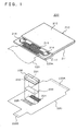
- Fig. 1 is an exploded perspective view illustrating the overall configuration of
a
liquid crystal device 200, which is the electro-optical device of the present embodiment. Theliquid crystal device 200 includes aliquid crystal panel 210, awiring substrate 220 that is connected to theliquid crystal panel 210, and a semiconductor device (semiconductor bare chip) 230 that is mounted on thewiring substrate 220. In theliquid crystal panel 210,substrates liquid crystal panel 210, there are cases where unillustrated polarizing plates or phase-difference plates are respectively adhered to outer surfaces of thesubstrates substrate extension portion 211T, which extends further out to the surrounding area than the outer shape of thesubstrate 212, is disposed at thesubstrate 211.Wirings substrates substrate extension portion 211T, and leading end portions thereof are arranged, as input terminals, on a substrate end portion of the substrate extension portion 211T.Thewiring substrate 220 includes a base material constituted by an insulating resin, such as a polyester resin or a polyimide resin, and a wiring pattern constituted by a conductor such as copper or the like. Thewiring substrate 220 is preferably configured as a flexible printed circuit (having flexibility and elasticity) in which the base material is formed at a thickness of about 50 µm to 1 mm. In this case, thewiring substrate 220 includes a structure described later so that a more reliable and uniform conductively connected state of conductively joined portions can be realized because it becomes easier to concentrate pressure applied at the time of mounting at the conductively joined portions formed by a method described later. Included in this wiring pattern are a panel-side wiring terminal 221, which is conductively connected to a panel-side connection portion 220A electrically connected to the input terminals of theliquid crystal panel 210, and a device-side wiring terminal 225, which is conductively connected to a device-side connection portion 220B connected to another circuit substrate and the like within the electronic device. In the present embodiment, a metal such as copper or aluminium, or a material where a surface-conductive layer constituted by copper, nickel or aluminium is adhered and formed at portions of surfaces of various metals that are to be connected to atleast electrodes wiring terminals semiconductor device 230 includes theelectrodes electrodes electrodes wiring terminals electrodes electrodes semiconductor device 230 is mounted on thewiring substrate 220 via an anisotropicconductive film 233 so that theelectrode 235 is conductively connected to thewiring terminal 225. - Fig. 2 is a perspective view illustrating when the
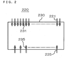
semiconductor device 230 mounted on the substrate is seen from a back surface side of thewiring substrate 220 with respect to theliquid crystal device 200. As shown in Fig. 2, thewiring terminals electrodes wiring terminals wiring substrates 220 are formed smaller than the width (width seen in the illustrated left and right directions) of thesemiconductor device 230. Here, at least the widths of all of thewiring terminals electrodes semiconductor device 230 are formed so as to have substantially the same value. Thus, because a reaction force received from each wiring terminal becomes substantially uniform whenplural electrodes semiconductor device 230 are pressure-contacted to thewiring terminals - Fig. 3 is an enlarged partial cross-sectional view showing the conductively
connected structure of the
wiring substrate 220 and thesemiconductor device 230. As shown in Fig. 3, in the present embodiment, thewiring terminals electrodes wiring terminals wiring terminals electrodes electrodes wiring terminals electrodes wiring terminals electrodes wiring terminals electrodes semiconductor device 230 easily occurs.In the present embodiment, as shown in Fig. 1, mounting is conducted by a method where pressure is applied, with respect to thesubstrate 220, to thesemiconductor device 230 via the anisotropicconductive film 233 on the surface of thewiring substrate 220 and heat is applied between thewiring substrate 220 and thesemiconductor device 230. In actuality, thesemiconductor device 230 is heated with a pressurizing and heating head, and the anisotropicconductive film 233 is heated by heat transmitted thereto. The anisotropicconductive film 233 is a film where the microscopicconductive particles 233a are dispersed in the insulating base material constituted by a thermoplastic resin or a thermosetting resin. As theconductive particles 233a, particles configured by a metal such as Ni or the like, or particles where a conductive layer of Ni plating or the like is formed on the surfaces of particles constituted by a synthetic resin, are used. There are no particular limitations on the particle diameter of theconductive particles 233a as long as it does not hinder the stability and reliability of the joined portions between the wiring terminals and the electrodes resulting from embedding. However, the particle diameter is preferably within the range of 0.1 µm to 5.0 µm. When the particle diameter of theconductive particles 233a is less than this range, the effect resulting from the embedding of the conductive particles or an anchor effect drops. When the particle diameter exceeds this range, the contact area of the conductively joined portions between the wiring terminals and the electrodes is reduced, and the stability and reliability of the conductively joined portions drop. In the present embodiment, thesemiconductor device 230 is gripped by, for example, the unillustrated pressurizing and heating head and pressurized and adhered to the surface of thewiring substrate 220 via the anisotropicconductive film 233. Then, while heating, thesemiconductor device 230 is pressurized, with respect to thewiring substrate 220, by a predetermined pressure. Thus, the base material of the anisotropicconductive film 233 is temporarily softened, and thewiring terminals electrodes conductive particles 233a. Although this point is the same as in conventional mounting methods, in the case of the present embodiment, the widths of thewiring terminals electrodes wiring terminals electrodes wiring terminals electrodes conductive particles 233a are present, theconductive particles 233a become embedded in the surface of theelectrodes conductive particles 233a are constituted by a material having a higher hardness than the surface portions of theelectrodes electrodes semiconductor device 230 is strengthened due to the anchor effect thereof. It should be noted that, although theconductive particles 233a have the same hardness as the top portions of thewiring terminals conductive particles 233a may also be constituted by a material having a higher hardness than the top portions of thewiring terminals conductive particles 233a also become embedded in thewiring terminals 221 and 225.The base material of the anisotropicconductive film 233 is, as described above, hardened by heating at the time of mounting (in the case of the thermosetting resin) or by cooling after the heating (in the case of the thermoplastic resin), to thereby adhere thewiring substrate 220 and thesemiconductor device 230 together. This base material functions as an adhesive and fulfils the role of retaining the conductively joined state between thewiring terminals electrodes conductive film 233 is temporarily softened at the time of mounting, which results in a structure where the space between thewiring substrate 220 and thesemiconductor device 230 is completely filled. - Fig. 4 is an enlarged cross-sectional view illustrating the structure of the
electrodes semiconductor device 230 prior to the mounting step. In thesemiconductor device 230 of the present embodiment, theelectrodes wiring terminals electrodes wiring terminals electrodes electrodes wiring terminals 221 and 225 (not illustrated in Fig. 4) and collapse of the overall shapes of the electrodes resulting from the pressure applied at the time of mounting can be prevented. Also, even if the material of the surface-conductive layer is an expensive material such as gold, the use amount thereof can be reduced, whereby manufacturing costs can be reduced. - Fig. 5 illustrates an electrode structure, which is different from that of the
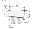
above-described embodiment, of a semiconductor device 230' prior to the mounting
step. The semiconductor device 230' has a structure where an electrode pad 230a' is
formed on a surface of a semiconductor layer of the semiconductor device 230' and
electrodes 231' and 235' for configuring protruding electrodes are joined to a surface
of the electrode pad 230a'. By configuring the electrodes in this manner, the
electrode pad 230a' can be formed with a material having excellent conductive
connectivity with respect to the semiconductor layer of the semiconductor device 230',
and the electrodes 231' and 235' can be formed with a material having characteristics
that are suitable with respect to conductive joining with the
wiring terminals 221 and 225 (not illustrated in Fig. 5). Thus, an excellent conductively connected state can be realized. The electrodes 231' and 235' shown in Fig. 5 are disposed with a cross-sectional shape having a convexly curving surface approximating a semicircular shape. When electrodes of this shape are manufactured, there are the advantages that labor for precisely molding the electrode shapes is not required and the electrodes can be formed at a relatively low cost by a method such as printing or welding a low-melting metal. - Fig. 6 illustrates an electrode structure, which is different from that of the
above-described embodiment, of a
semiconductor device 230" prior to the mounting step. In thesemiconductor device 230", an electrode pad 230a" that is conductively brought into contact with a semiconductor layer is selectively formed at two places in the width direction, andelectrodes 231" and 235" are formed on these electrode pads 230a" so as to cover both of the electrode pads 230a" of the two places. The electrodes pads 230a" can be easily formed by using an ordinary patterning technique such as photolithography. By configuring the electrodes in this manner, theelectrodes 231" and 235" reflect a convexo-concave structure configured by the electrode pads 230a" of the undersurface and are disposed with surfaces having a convexo-concave shape in the width direction thereof. That is, recessedportions 231d" and 235d" are formed in a width-direction center portion in the surfaces of theelectrodes 231" and 235". By making the interval between the electrode pads 230a" substantially equal to the widths of the wiring terminals, the recessed portions 213d" and 235d" are constituted by a dimension corresponding to the widths of thewiring terminals 221 and 225 (not illustrated in Fig. 6). Thus, due to the fact that the recessedportions 231d" and 235d" are present, there is the advantage that the applied pressure for obtaining the embedded state (the aforementioned embedding amount "Dp") of thewiring terminals semiconductor device 230" can be further reduced and product yield can be increased. - Fig. 7(a) is a perspective view illustrating the shape of the leading end
portion vicinity of the
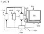
wiring terminals wiring terminals wiring terminals wiring terminals wiring terminals electrodes wiring terminals electrodes wiring terminals electrodes wiring terminals electrodes wiring terminals liquid crystal device 200 is used as a display device in an electronic device. Fig. 8 is a schematic structural diagram illustrating the overall configuration of the present embodiment. The electronic device illustrated here includes the sameliquid crystal device 200 described above and control means 1200 that controls theliquid crystal device 200. Here, theliquid crystal device 200 includes, as mentioned above, theliquid crystal panel 210, thewiring substrate 220 and the semiconductor device 230.Also, the control means 1200 includes a displayinformation output source 1210, a displayinformation processing circuit 1220, apower circuit 1230 and a timing generator 1240.The displayinformation output source 1210 is disposed with a memory comprising a ROM (Read Only Memory), a RAM (Random Access Memory) and the like; a storage unit comprising an electromagnetic recording disk, a light recording disk and the like; and a tuning circuit that tunes and outputs a digital image signal. The displayinformation output source 1210 is configured so as to supply, to the displayinformation processing circuit 1220, display information in the form of an image signal of a predetermined format on the basis of various kinds of clock signals generated by the timing generator 1240.The displayinformation processing circuit 1220 is disposed with various known circuits such as a serial-parallel conversion circuit, an amplification/inversion circuit, a rotation circuit, a gamma correction circuit and a clamp circuit. The displayinformation processing circuit 1220 implements processing of inputted display information and supplies this image information together with a clock signal CLK to thesemiconductor device 230 via thewiring substrate 220. Thesemiconductor device 230 includes a scanning line drive circuit, a data line drive circuit and a testing circuit. Also, thepower circuit 1230 respectively supplies a predetermined voltage to the aforementioned various constituent elements. - Fig. 9 illustrates a
mobile telephone 2000, which is an embodiment of the electronic device pertaining to the present invention. In themobile telephone 2000, acircuit board 2001 is disposed inside acase body 2010 and theliquid crystal device 200 is mounted with respect to thecircuit board 2001.Operational buttons 2020 are arranged on a front surface of thecase body 2010, and anantenna 2030 is attached so as to be pulled out from and pushed into an end portion. A speaker is disposed inside areceiver portion 2040, and a microphone is built inside atransmitter portion 2050. Theliquid crystal device 200 disposed inside thecase body 2010 is configured so that it is possible to view a display surface (the aforementioned liquid crystal charging region or display region) thereof through a display window 2060.It should be noted that, although the semiconductor device is mounted on the wiring substrate via the anisotropic conductive film (ACF) in the above-described embodiment, the present invention is not limited to this configuration. It is possible to use various joining methods, such as various kinds of mounting methods used in flip-flop mounting, such as joining with solder or lead-free solder (Ag-Sn, etc.), thermocompression of like Au members, various metal joining methods such as joining by supersonic vibration, conductive resin joining methods, anisotropic conductive paste (ACP) joining methods, and insulating resin joining methods such as NCF (Non-Conductive Film) joining methods and NCP (Non-Conductive Paste) joining methods.The electro-optical device and electronic device of the invention are not limited to the examples illustrated and can be variously modified within a range that does not deviate from the scope of the invention. For example, the liquid crystal panel illustrated in each of the above embodiments can also be applied to a liquid crystal device of a passive matrix type or to an active matrix liquid crystal device using an active element such as a TFT (Thin Film Transistor) or a TFD (Thin Film Diode).Although description was given in the aforementioned embodiments of a case where the invention was applied to a liquid crystal device as the electro-optical device, the present invention is not limited to this. The invention can be applied to various kinds of electro-optical devices such as electro-luminescence devices, particularly organic electro-luminescence devices and inorganic electro-luminescence devices, plasma display devices, FED (Field Emission Display) devices, surface-conduction electron-emitter display, LED (light-emitting diode) display devices, electrophoretic display devices, small televisions using a thin cathode ray tube or liquid crystal shutter, and devices using digital micro-mirror devices (DMD). As described above, according to the invention, the reliability of conductively joined portions in a mounting structure of a semiconductor device can be improved even if the number of wirings and the number of electrodes increase and wiring intervals and electrode intervals are narrowed.
Claims (19)
- A semiconductor device mounting method in which a semiconductor device disposed with an electrode is mounted on a substrate disposed with a wiring terminal, wherein
the width of one of the electrode and the wiring terminal is formed smaller than the width of the other, and
pressure is mutually applied to the semiconductor device and the substrate so that the one of the electrode and the wiring terminal becomes embedded in a surface of the other. - A semiconductor device mounting method in which a semiconductor device disposed with an electrode is mounted on a substrate disposed with a wiring terminal, wherein
the width of one of the electrode and the wiring terminal that is constituted by a material having a high hardness is formed smaller than the width of the other, and
pressure is mutually applied to the semiconductor device and the substrate. - The semiconductor device mounting method of claim 1 or 2, wherein the electrode and the wiring terminal are both plurally disposed and the widths of all of the one conductively connected to the other are formed to be substantially the same.
- A semiconductor device mounting method in which a semiconductor device disposed with an electrode is mounted on a substrate disposed with a wiring terminal, wherein
the width of the wiring terminal is formed smaller than the width of the electrode, and
pressure is mutually applied to the semiconductor device and the substrate so that the wiring terminal becomes embedded in a surface of the electrode. - A semiconductor device mounting method in which a semiconductor device disposed with an electrode is mounted on a substrate disposed with a wiring terminal, wherein
the width of the wiring terminal constituted by a material of a higher hardness than that of the electrode is formed smaller than the width of the electrode, and
pressure is mutually applied to the semiconductor device and the substrate. - The semiconductor device mounting method of claim 4 or 5, wherein the wiring terminal is configured so as to extend from in front of the electrode to as far as a position crossing the electrode.
- The semiconductor device mounting method of any one of claims 1 to 6, wherein microscopic conductive particles are intervened between the electrode and the wiring terminal and pressure is mutually applied to the semiconductor device and the substrate.
- The semiconductor device mounting method of any one of claims 1 to 7, wherein an adhesive is disposed between the semiconductor device and the substrate and the adhesive is hardened in a pressurized state.
- A semiconductor device mounting structure including a semiconductor device disposed with an electrode and a substrate disposed with a wiring terminal that is conductively connected to the electrode, wherein
the width of one of the electrode and the wiring terminal is formed smaller than the width of the other, and
the one of the electrode and the wiring terminal is embedded in a surface of the other. - The semiconductor device mounting structure of claim 9, wherein the cross-sectional shape of the one is a shape where the width becomes smaller towards the other.
- The semiconductor device mounting structure of claim 9 or 10, wherein the one is constituted by a material having a higher hardness than that of the other.
- The semiconductor device mounting structure of any one of claims 9 to 11, wherein the electrode and the wiring terminal are both plurally disposed, and the widths of all of the one conductively connected to the other are formed to be substantially the same.
- A semiconductor device mounting structure including a semiconductor device disposed with an electrode and a substrate disposed with a wiring terminal that is conductively connected to the electrode, wherein
the width of the wiring terminal is formed smaller than the width of the electrode, and
the wiring terminal is embedded in a surface of the electrode. - An electro-optical device including an electro-optical panel retaining an electro-optical substance, a wiring substrate including a wiring terminal conductively connected to the electro-optical panel and a semiconductor device including an electrode conductively connected to the wiring terminal, wherein
the width of one of the wiring terminal and the electrode is formed smaller than the width of the other, and
the one is conductively connected to the other in a state where the one is embedded in a surface of the other. - An electro-optical device including an electro-optical panel retaining an electro-optical substance, a wiring substrate including a wiring terminal conductively connected to the electro-optical panel and a semiconductor device including an electrode conductively connected to the wiring terminal, wherein
the width of the wiring terminal is formed smaller than the width of the electrode, and
the wiring terminal is embedded in a surface of the electrode. - An electronic device including the semiconductor device mounting structure of any one of claims 9 to 13.
- An electronic device including the electro-optical device of claim 14 or 15 and control means that controls the electro-optical device.
- A method of manufacturing an electro-optical device that includes an electro-optical panel retaining an electro-optical substance, a wiring substrate including a wiring terminal conductively connected to the electro-optical panel and a semiconductor device including an electrode conductively connected to the wiring terminal, wherein
the width of one of the wiring terminal and the electrode is formed smaller than the width of the other, and
the one is conductively connected to the other by embedding the one in a surface of the other. - A method of manufacturing an electro-optical device that includes an electro-optical panel retaining an electro-optical substance, a wiring substrate including a wiring terminal conductively connected to the electro-optical panel and a semiconductor device including an electrode conductively connected to the wiring terminal, wherein
the width of the wiring terminal is formed smaller than the width of the electrode, and
the wiring terminal is embedded in a surface of the electrode.
Applications Claiming Priority (4)
| Application Number | Priority Date | Filing Date | Title |
|---|---|---|---|
| JP2002240776 | 2002-08-21 | ||
| JP2002240776 | 2002-08-21 | ||
| JP2003197276 | 2003-07-15 | ||
| JP2003197276A JP3722137B2 (en) | 2002-08-21 | 2003-07-15 | Semiconductor device mounting method, semiconductor device mounting structure, electro-optical device, electro-optical device manufacturing method, and electronic apparatus |
Publications (2)
| Publication Number | Publication Date |
|---|---|
| EP1391922A2 true EP1391922A2 (en) | 2004-02-25 |
| EP1391922A3 EP1391922A3 (en) | 2006-04-19 |
Family
ID=31190383
Family Applications (1)
| Application Number | Title | Priority Date | Filing Date |
|---|---|---|---|
| EP03255363A Ceased EP1391922A3 (en) | 2002-08-21 | 2003-08-13 | Semiconductor device mounting method, semiconductor device mounting structure, electro optical device, electro-optical device manufacturing method and electronic device |
Country Status (6)
| Country | Link |
|---|---|
| US (1) | US7180196B2 (en) |
| EP (1) | EP1391922A3 (en) |
| JP (1) | JP3722137B2 (en) |
| KR (2) | KR100564172B1 (en) |
| CN (2) | CN1229854C (en) |
| TW (1) | TWI246131B (en) |
Families Citing this family (12)
| Publication number | Priority date | Publication date | Assignee | Title |
|---|---|---|---|---|
| JP3833669B2 (en) | 2004-04-08 | 2006-10-18 | シャープ株式会社 | Semiconductor device and manufacturing method of semiconductor device |
| KR20060005910A (en) * | 2004-07-14 | 2006-01-18 | (주)아이셀론 | Display driving chip and IC chip and flexible substrate bonding structure and method using AU flat bump |
| JP4749177B2 (en) * | 2006-02-15 | 2011-08-17 | パナソニック株式会社 | Connection structure and method of manufacturing connection structure |
| JP2009080361A (en) * | 2007-09-27 | 2009-04-16 | Sanyo Electric Co Ltd | Plasma display device |
| JP5125632B2 (en) * | 2008-03-10 | 2013-01-23 | セイコーエプソン株式会社 | Mounting structure and electro-optical device |
| JP4814277B2 (en) * | 2008-04-18 | 2011-11-16 | ソニーケミカル&インフォメーションデバイス株式会社 | Bonded body, method for manufacturing the bonded body, and anisotropic conductive film used for the bonded body |
| JP5452290B2 (en) * | 2010-03-05 | 2014-03-26 | ラピスセミコンダクタ株式会社 | Display panel |
| CN105493015B (en) * | 2015-02-06 | 2019-04-30 | 深圳市柔宇科技有限公司 | capacitive touch screen |
| JP6750439B2 (en) * | 2016-09-30 | 2020-09-02 | セイコーエプソン株式会社 | Electronic device, electronic device device, electronic device, and moving body |
| US10937707B2 (en) * | 2017-02-22 | 2021-03-02 | Kyocera Corporation | Wiring substrate, electronic device, and electronic module |
| KR20230019692A (en) | 2021-08-02 | 2023-02-09 | 삼성전자주식회사 | Chip on film package and display apparatus including the same |
| CN114040568A (en) * | 2021-10-29 | 2022-02-11 | 株洲中车时代半导体有限公司 | IGCT and high-power semiconductor device |
Family Cites Families (15)
| Publication number | Priority date | Publication date | Assignee | Title |
|---|---|---|---|---|
| JPS6049638A (en) * | 1983-08-26 | 1985-03-18 | Sharp Corp | Construction of electronic parts |
| AU645283B2 (en) | 1990-01-23 | 1994-01-13 | Sumitomo Electric Industries, Ltd. | Substrate for packaging a semiconductor device |
| US5592365A (en) | 1993-12-21 | 1997-01-07 | Sharp Kabushiki Kaisha | Panel assembly structure and panel assembling method capable of achieving a highly reliable connection of electrode terminals even when the electrode terminals have a fine pitch |
| US5457879A (en) * | 1994-01-04 | 1995-10-17 | Motorola, Inc. | Method of shaping inter-substrate plug and receptacles interconnects |
| JP3383081B2 (en) | 1994-07-12 | 2003-03-04 | 三菱電機株式会社 | Electronic component manufactured using anodic bonding and method of manufacturing electronic component |
| JPH09260424A (en) * | 1996-03-25 | 1997-10-03 | Toshiba Corp | Semiconductor device and manufacturing method thereof |
| US5926694A (en) * | 1996-07-11 | 1999-07-20 | Pfu Limited | Semiconductor device and a manufacturing method thereof |
| US6137063A (en) * | 1998-02-27 | 2000-10-24 | Micron Technology, Inc. | Electrical interconnections |
| JPH11251363A (en) * | 1998-03-03 | 1999-09-17 | Olympus Optical Co Ltd | Flip chip mounting method and flip chip mounting structure |
| JP3660175B2 (en) * | 1998-11-25 | 2005-06-15 | セイコーエプソン株式会社 | Mounting structure and method of manufacturing liquid crystal device |
| JP3498634B2 (en) * | 1999-05-31 | 2004-02-16 | 関西日本電気株式会社 | Method for manufacturing semiconductor device |
| DE19927749A1 (en) * | 1999-06-17 | 2000-12-28 | Siemens Ag | Electronic arrangement used as a semiconductor chip has electrical contacts on a first surface with a flexible elevation made of an insulating material |
| JP3820812B2 (en) * | 1999-08-04 | 2006-09-13 | セイコーエプソン株式会社 | IC chip mounting structure, liquid crystal device and electronic device |
| JP2001223243A (en) * | 2000-02-14 | 2001-08-17 | Seiko Epson Corp | Semiconductor device and its manufacturing method, circuit board, and electronic equipment |
| DE10163799B4 (en) * | 2000-12-28 | 2006-11-23 | Matsushita Electric Works, Ltd., Kadoma | Semiconductor chip mounting substrate and method of manufacturing such a mounting substrate |
-
2003
- 2003-07-15 JP JP2003197276A patent/JP3722137B2/en not_active Expired - Lifetime
- 2003-08-12 TW TW092122159A patent/TWI246131B/en not_active IP Right Cessation
- 2003-08-13 EP EP03255363A patent/EP1391922A3/en not_active Ceased
- 2003-08-20 KR KR1020030057472A patent/KR100564172B1/en not_active Expired - Lifetime
- 2003-08-20 US US10/644,603 patent/US7180196B2/en not_active Expired - Lifetime
- 2003-08-20 CN CNB03153919XA patent/CN1229854C/en not_active Expired - Lifetime
- 2003-08-21 CN CNU032766777U patent/CN2704863Y/en not_active Expired - Lifetime
- 2003-08-21 KR KR20-2003-0026861U patent/KR200331933Y1/en not_active Ceased
Also Published As
| Publication number | Publication date |
|---|---|
| US7180196B2 (en) | 2007-02-20 |
| US20040094846A1 (en) | 2004-05-20 |
| KR100564172B1 (en) | 2006-03-31 |
| CN2704863Y (en) | 2005-06-15 |
| KR20040018158A (en) | 2004-03-02 |
| KR200331933Y1 (en) | 2003-11-01 |
| TWI246131B (en) | 2005-12-21 |
| JP3722137B2 (en) | 2005-11-30 |
| TW200406857A (en) | 2004-05-01 |
| CN1229854C (en) | 2005-11-30 |
| CN1490646A (en) | 2004-04-21 |
| JP2004140331A (en) | 2004-05-13 |
| EP1391922A3 (en) | 2006-04-19 |
Similar Documents
| Publication | Publication Date | Title |
|---|---|---|
| KR100457900B1 (en) | Manufacturing method for manufacturing electro-optical device, and electro-optical device | |
| JP3622665B2 (en) | Connection structure, electro-optical device and electronic apparatus | |
| TWI390310B (en) | Liquid crystal display device and fabricating method thereof | |
| KR100699823B1 (en) | Low Cost Flexible Film Package Module and Manufacturing Method Thereof | |
| JP4888462B2 (en) | Electronic component mounting structure | |
| US6266119B1 (en) | Liquid crystal apparatus and production process thereof | |
| US6738123B1 (en) | Drive circuit connection structure including a substrate, circuit board, and semiconductor device, and display apparatus including the connection structure | |
| US6031590A (en) | Structure and method of mounting driver IC using anisotropic conductive film in liquid crystal display device | |
| US7180196B2 (en) | Semiconductor device mounting method, semiconductor device mounting structure, electro-optical device, electro-optical device manufacturing method and electronic device | |
| KR20000071406A (en) | Semiconductor device, semiconductor device mounting structure, liquid crystal device, and electronic apparatus | |
| US20080005897A1 (en) | Flexible wiring sheet, display apparatus and manufacturing method thereof | |
| JP5125314B2 (en) | Electronic equipment | |
| KR20130011403A (en) | Flexible circuit board | |
| US7554643B2 (en) | Electro-optical device, electronic apparatus, and interface board | |
| JPH10209581A (en) | Printed wiring board, liquid crystal display device and electronic equipment | |
| KR100707587B1 (en) | Method for manufacturing electronic component mounting body and electro-optical device | |
| JP2001230001A (en) | Connection structure, electro-optical device and electronic equipment | |
| JPH1096944A (en) | Electrical connection structure and liquid crystal display | |
| JP2007165745A (en) | Mounting structure, electro-optical device, and electronic apparatus | |
| JP4370994B2 (en) | Mounting board and display device | |
| JPH09305121A (en) | Circuit connection structure, display device having this circuit connection structure, and TCP structure | |
| JP2004140332A (en) | Semiconductor device mounting method, semiconductor device mounting structure, electro-optical device, electro-optical device manufacturing method, and electronic apparatus | |
| JP2002244146A (en) | Method for internal connection of flat panel display provided with opaque substrate, and device formed by the method | |
| US7744996B2 (en) | Adhesive structure and method for manufacturing the same | |
| JP3026896B2 (en) | Liquid crystal device |
Legal Events
| Date | Code | Title | Description |
|---|---|---|---|
| PUAI | Public reference made under article 153(3) epc to a published international application that has entered the european phase |
Free format text: ORIGINAL CODE: 0009012 |
|
| AK | Designated contracting states |
Kind code of ref document: A2 Designated state(s): AT BE BG CH CY CZ DE DK EE ES FI FR GB GR HU IE IT LI LU MC NL PT RO SE SI SK TR |
|
| AX | Request for extension of the european patent |
Extension state: AL LT LV MK |
|
| PUAL | Search report despatched |
Free format text: ORIGINAL CODE: 0009013 |
|
| AK | Designated contracting states |
Kind code of ref document: A3 Designated state(s): AT BE BG CH CY CZ DE DK EE ES FI FR GB GR HU IE IT LI LU MC NL PT RO SE SI SK TR |
|
| AX | Request for extension of the european patent |
Extension state: AL LT LV MK |
|
| 17P | Request for examination filed |
Effective date: 20060919 |
|
| AKX | Designation fees paid |
Designated state(s): DE FR GB |
|
| 17Q | First examination report despatched |
Effective date: 20071113 |
|
| STAA | Information on the status of an ep patent application or granted ep patent |
Free format text: STATUS: THE APPLICATION HAS BEEN REFUSED |
|
| 18R | Application refused |
Effective date: 20100709 |