EP1387392B1 - Elektrostatischer Greifer - Google Patents
Elektrostatischer Greifer Download PDFInfo
- Publication number
- EP1387392B1 EP1387392B1 EP03000853.6A EP03000853A EP1387392B1 EP 1387392 B1 EP1387392 B1 EP 1387392B1 EP 03000853 A EP03000853 A EP 03000853A EP 1387392 B1 EP1387392 B1 EP 1387392B1
- Authority
- EP
- European Patent Office
- Prior art keywords
- gripping device
- wafer
- circuit board
- gripping
- electrodes
- Prior art date
- Legal status (The legal status is an assumption and is not a legal conclusion. Google has not performed a legal analysis and makes no representation as to the accuracy of the status listed.)
- Expired - Lifetime
Links
Images

Classifications
-
- H—ELECTRICITY
- H01—ELECTRIC ELEMENTS
- H01L—SEMICONDUCTOR DEVICES NOT COVERED BY CLASS H10
- H01L21/00—Processes or apparatus adapted for the manufacture or treatment of semiconductor or solid state devices or of parts thereof
- H01L21/67—Apparatus specially adapted for handling semiconductor or electric solid state devices during manufacture or treatment thereof; Apparatus specially adapted for handling wafers during manufacture or treatment of semiconductor or electric solid state devices or components ; Apparatus not specifically provided for elsewhere
- H01L21/683—Apparatus specially adapted for handling semiconductor or electric solid state devices during manufacture or treatment thereof; Apparatus specially adapted for handling wafers during manufacture or treatment of semiconductor or electric solid state devices or components ; Apparatus not specifically provided for elsewhere for supporting or gripping
- H01L21/6831—Apparatus specially adapted for handling semiconductor or electric solid state devices during manufacture or treatment thereof; Apparatus specially adapted for handling wafers during manufacture or treatment of semiconductor or electric solid state devices or components ; Apparatus not specifically provided for elsewhere for supporting or gripping using electrostatic chucks
-
- Y—GENERAL TAGGING OF NEW TECHNOLOGICAL DEVELOPMENTS; GENERAL TAGGING OF CROSS-SECTIONAL TECHNOLOGIES SPANNING OVER SEVERAL SECTIONS OF THE IPC; TECHNICAL SUBJECTS COVERED BY FORMER USPC CROSS-REFERENCE ART COLLECTIONS [XRACs] AND DIGESTS
- Y10—TECHNICAL SUBJECTS COVERED BY FORMER USPC
- Y10T—TECHNICAL SUBJECTS COVERED BY FORMER US CLASSIFICATION
- Y10T279/00—Chucks or sockets
- Y10T279/23—Chucks or sockets with magnetic or electrostatic means
-
- Y—GENERAL TAGGING OF NEW TECHNOLOGICAL DEVELOPMENTS; GENERAL TAGGING OF CROSS-SECTIONAL TECHNOLOGIES SPANNING OVER SEVERAL SECTIONS OF THE IPC; TECHNICAL SUBJECTS COVERED BY FORMER USPC CROSS-REFERENCE ART COLLECTIONS [XRACs] AND DIGESTS
- Y10—TECHNICAL SUBJECTS COVERED BY FORMER USPC
- Y10T—TECHNICAL SUBJECTS COVERED BY FORMER US CLASSIFICATION
- Y10T29/00—Metal working
- Y10T29/49—Method of mechanical manufacture
- Y10T29/49002—Electrical device making
- Y10T29/49117—Conductor or circuit manufacturing
-
- Y—GENERAL TAGGING OF NEW TECHNOLOGICAL DEVELOPMENTS; GENERAL TAGGING OF CROSS-SECTIONAL TECHNOLOGIES SPANNING OVER SEVERAL SECTIONS OF THE IPC; TECHNICAL SUBJECTS COVERED BY FORMER USPC CROSS-REFERENCE ART COLLECTIONS [XRACs] AND DIGESTS
- Y10—TECHNICAL SUBJECTS COVERED BY FORMER USPC
- Y10T—TECHNICAL SUBJECTS COVERED BY FORMER US CLASSIFICATION
- Y10T29/00—Metal working
- Y10T29/53—Means to assemble or disassemble
- Y10T29/5313—Means to assemble electrical device
- Y10T29/53196—Means to apply magnetic force directly to position or hold work part
Definitions
- the invention relates to a working on electrostatic principle gripper, in particular for use in the semiconductor industry.
- vacuum grippers are used, which can suck in the wafer by vacuum and thus transport it.
- semiconductor structures continue to shrink in size, more and more is being produced in a vacuum environment.
- vacuum grippers can not be used here.
- the insulating layer used is mostly aluminum (III) oxide ( US Pat. No. 6,272,002 B1 . US 6 122 159 A ).
- the document US Pat. No. 6,272,002 B1 also describes the use of zirconium oxide as a thermal attenuation layer and the production of an electrode by pressing and sintering a layer composite.
- an opposite voltage is applied to adjacent, oppositely poled electrodes.
- the electrodes now have a different charge than the component to be lifted, which leads to a force due to the electrostatic attraction. As a result of this force, the wafer gets stuck on the gripper and can then be moved. To remove the component, the electrodes are grounded.
- a disadvantage of the known grippers of this principle is that in the wafer by the voltage differences, a current flows, which depends on the conductivity of the wafer and the amount of voltage. This current leads to a heating of the wafer, which depends on its geometry and conductivity, as well as the applied voltage. As a result of this heating, warping and damage to the wafer may occur. This problem is due to the lack of convection, especially in a vacuum.
- the object of the invention is to develop an electrostatic gripper, which reduces the heating of the wafer to a minimum and can be operated with the lowest possible voltage.
- the zirconium oxide used in the gripper according to the invention which is used, for example, for the production of fuel cells, is available in layer thicknesses of 50-300 ⁇ m and therefore does not need to be sanded or only slightly ground. It is also conceivable layer thicknesses below 50 microns, which can be achieved by grinding or by applying the Zirkoniumoxid für in a CVD or sputtering process. In the latter way, layer thicknesses in the range of a few atomic diameter are possible. Another advantage arises from the higher hardness of zirconia over alumina. Both during manufacture and during operation, the layer is damaged less quickly. The layer also remains smooth, which avoids damage to the wafer even after prolonged use. Another advantage is the very high electrical resistivity of about 10 14 ⁇ m, so the layer thickness can be kept very small.
- the gripper according to the invention can be operated with a DC voltage of only 200 to 900 V, which leads to greatly reduced currents in the wafer.
- known electrostatic grippers are operated with voltages between 1 and 6 kV.
- the gripper according to the invention further comprises two or more electrode pairs, which are applied to a circuit board. So the pairs of electrodes can warming-insensitive areas of the wafer are used.
- the circuit board serves as a holder of the electrode pairs and at the same time there is the power supply included.
- the existing predominantly zirconium oxide layer of the gripper invention may also contain a variety of additives. So the mechanical and electrical properties can be changed.
- zirconium oxide stabilized with yttrium oxide has proved to be particularly advantageous as an insulating layer. But also an insulating layer of pure zirconium oxide is conceivable.
- a development of the invention has a holder of a flexible circuit board. This allows the gripper to adapt to the shape of the wafer.
- This circuit board may conveniently be a printed circuit board, which is inexpensive to produce in one operation.
- the development of the invention has electrode pairs, which have a round, rectangular or finger-like shape, and thus take up only a small area.
- pairs of electrodes can be constructed so that one pole from the other pole, e.g. circular, is enclosed.
- the gripper with DC voltages operated under 900V.
- the layer thicknesses of the zirconium oxide By reducing the layer thicknesses of the zirconium oxide and optimizing the geometry, even voltages below 300 V are conceivable.
- the heating of the wafer is minimal.
- impurities of the wafer are reduced by attracted dust particles and the electrical circuit for operating the gripper is much easier.
- the operating costs are also reduced by lower power consumption.
- an alternating voltage can be applied briefly when the component is released. This avoids that the wafer does not dissolve due to the presence of electrostatic charge.
- An expedient embodiment has the electrode pairs spaced apart so that the wafer can be gripped at the edge.
- the advantages of the compact design of the electrode pairs are optimally utilized. By gripping on the edge, heating in sensitive areas of the wafer can be further reduced.
- the gripper For lifting, the gripper according to a further embodiment has three arranged on a circular path electrode pairs, which are ideally arranged at 120 ° angle to the wafer. Thus, the weight of the wafer is distributed equally to the three pairs of electrodes.
- a method for producing an electrostatic An inventive gripper can be prepared as follows.
- pairs of electrodes are placed on a flexible circuit board. Then it becomes a network layer brought to the electrodes.
- Indium for example, which can be applied to the electrodes beforehand in a galvanic process in a layer thickness of approximately 10 ⁇ m, is also suitable for this purpose.
- a layer of zinc can also improve the bonding of the different materials.
- the zirconium oxide layer is then placed on the indium layer.
- an insulating layer is applied. Then the layers are pressed together, joining them together in a cold-welding operation. This process benefits a rough surface of a ziconium oxide disk.
- the material used for the insulating layer may, as provided in a development of the method, be useful to stick the insulating layer, or to use an already coated with adhesive insulating layer.
- a material for such an insulating layer is, as provided in one embodiment of the method, in particular aluminum (III) oxide. This is inexpensive and is used by default as an insulating material in the semiconductor industry.
- the electrode pairs can first be applied to another flexible circuit board, for example in the etching process.
- the pairs of electrodes are then placed on the circuit board with the other circuit board.
- the production of the gripper can not be done in one operation, but the process is appropriate if, because of the geometry of the electrodes (eg very small, distance of the electrodes very low) a production in one step technically not feasible or with greater effort connected is.
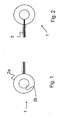
- the bipolar electrodes 1, which are in Fig. 1 can be seen in plan view, consist of an outer ring 2 as an electrode which surrounds the other electrode 2b.
- the inner electrode 2b has its power supply 3 on top of the flexible printed circuit board 10 (FIG. Fig. 3 ). Looking at the electrode from above ( Fig. 2 ), the power supply 3 for the inner electrode can be seen.
- a DC voltage is applied to the inner and outer electrodes. The resulting electrostatic field leads to the attraction of the wafer 5.
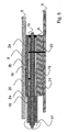
- the electrostatic holder 4 which is in Fig. 3 can be seen in an exploded view, consists of the flexible, printed circuit board 10, on which the conductor tracks 11 for the electrodes 1a-1c are printed.
- the individual layers that make up the gripper, as shown before the assembly.
- the individual layers are (except for the pairs of electrodes) provided only with the upper gripping element with reference numerals.
- the electrodes 1a-1c contain the in Fig. 1 and 2 to be seen bipolar electrode pairs 2a, 2b.
- the conductor tracks 11 each consist of two lines for supplying voltage to the electrodes 1a-1c.
- the above-described layer structure comprising an insulating layer zirconium oxide 6, the bipolar electrode pairs 1a-1c, an insulating layer on the rear side 8 and a base plate 9 for better stability forms an electrostatic gripping element 13a-13c according to the invention.
- the insulating layer is provided in this embodiment with an adhesive film (not shown), whereby the bond improves and air pockets are largely prevented.
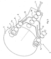
- the embodiment has three pairs of electrodes or gripping elements, which are arranged at an angle of 120 ° on a circular path. Thus, the wafer can possibly be caught at the edges.
- the gripping elements 13a-13c consist of the layered structure shown above.
- the aim of the pressing process is to produce a cold weld.
- indium can be used as a network layer (not shown) between the zirconium oxide layer 6 and the electrodes 1a-1c in order to produce an optimum connection between oxide layer and electrodes.
- the power is supplied by the conductor tracks now in the circuit board 11, whose course was determined by the previously provided recesses 12.
- Fig. 5 shows a sectional view of a gripping element including a captured wafer.
- the wafer 5 below which is the insulating layer of zirconia 6, and then comes the bipolar electrode pair consisting of inner 2b and outer 2a electrode separated by a ring of insulating material 20. Then comes the power supply of the outer electrode 15, which takes place via a conductive layer 19.
- the flexible circuit board 10 made of Kapton.
- the power supply of the inner electrode is made by the conductive layer 18 below and a connection through the circuit board 16, an underlying conductive layer 21 serves as a continuation to other electrodes or gripping elements on the gripper.
- an insulating layer of aluminum (III) oxide 8 below the bottom of a stable base plate 9.
- a channel 13 is still provided for the introduction of insulating material. Such channels serve to introduce insulating material into the channels between the electrodes.
- the lower layer 18 is provided for the inner, the upper layer 19 for the outer electrode.
- the inner electrode has a diameter of 18 mm, the outer an outer diameter of 37 mm.
- Nickel and indium layer are already applied galvanically on the copper electrodes.
- the electrostatic chuck By applying a voltage, the wafer 5 is attracted by electrostatic attraction. Operated at a voltage of 300 V, the electrostatic chuck according to the embodiment achieves a force of 6 N sufficient to lift a wafer.
- the gripper may e.g. be mounted on a robot arm and used for transport, positioning and to bring about any conceivable change in the position of the wafer.
Landscapes
- Engineering & Computer Science (AREA)
- Physics & Mathematics (AREA)
- Condensed Matter Physics & Semiconductors (AREA)
- General Physics & Mathematics (AREA)
- Manufacturing & Machinery (AREA)
- Computer Hardware Design (AREA)
- Microelectronics & Electronic Packaging (AREA)
- Power Engineering (AREA)
- Container, Conveyance, Adherence, Positioning, Of Wafer (AREA)
- Manipulator (AREA)
- Feeding Of Articles By Means Other Than Belts Or Rollers (AREA)
Applications Claiming Priority (2)
| Application Number | Priority Date | Filing Date | Title |
|---|---|---|---|
| DE10232080 | 2002-07-15 | ||
| DE10232080.2A DE10232080B4 (de) | 2002-07-15 | 2002-07-15 | Elektrostatischer Greifer und Verfahren zu dessen Herstellung |
Publications (3)
| Publication Number | Publication Date |
|---|---|
| EP1387392A2 EP1387392A2 (de) | 2004-02-04 |
| EP1387392A3 EP1387392A3 (de) | 2005-09-07 |
| EP1387392B1 true EP1387392B1 (de) | 2013-04-24 |
Family
ID=30010018
Family Applications (1)
| Application Number | Title | Priority Date | Filing Date |
|---|---|---|---|
| EP03000853.6A Expired - Lifetime EP1387392B1 (de) | 2002-07-15 | 2003-01-15 | Elektrostatischer Greifer |
Country Status (4)
| Country | Link |
|---|---|
| US (1) | US7075772B2 (ja) |
| EP (1) | EP1387392B1 (ja) |
| JP (1) | JP4159926B2 (ja) |
| DE (1) | DE10232080B4 (ja) |
Families Citing this family (13)
| Publication number | Priority date | Publication date | Assignee | Title |
|---|---|---|---|---|
| ES2527760T3 (es) * | 1998-07-23 | 2015-01-29 | Yeda Research And Development Co., Ltd. | Tratamiento de enfermedad de Crohn con copolímero 1 y polipéptidos |
| DE10232080B4 (de) * | 2002-07-15 | 2015-10-01 | Integrated Dynamics Engineering Gmbh | Elektrostatischer Greifer und Verfahren zu dessen Herstellung |
| JP2006026827A (ja) * | 2004-07-16 | 2006-02-02 | Aoi Electronics Co Ltd | 測長機能付きナノグリッパ装置 |
| JP4529012B2 (ja) * | 2004-07-16 | 2010-08-25 | アオイ電子株式会社 | ナノグリッパ装置 |
| WO2011077678A1 (ja) * | 2009-12-22 | 2011-06-30 | 株式会社アルバック | 基板保持装置 |
| US8672311B2 (en) * | 2010-06-01 | 2014-03-18 | Varian Semiconductor Equipment Associates, Inc. | Method of cooling textured workpieces with an electrostatic chuck |
| DE102010022625A1 (de) | 2010-06-04 | 2011-12-08 | Festo Ag & Co. Kg | Handhabungssystem zur Handhabung von Gegenständen |
| DE102010054483A1 (de) * | 2010-12-14 | 2012-06-14 | Manz Automation Ag | Mobile, transportable elektrostatische Substrathalteanordnung |
| DE102012019839B4 (de) * | 2012-10-09 | 2017-08-24 | Grenzebach Maschinenbau Gmbh | Verfahren und Vorrichtung für das Befördern großflächiger Platten in extremer Übergröße |
| DE102012019841B4 (de) | 2012-10-09 | 2022-01-05 | Grenzebach Maschinenbau Gmbh | Verfahren und Vorrichtung für das Umsetzen großflächiger Platten in extremer Übergröße |
| DE102012020679B4 (de) * | 2012-10-22 | 2022-01-05 | Grenzebach Maschinenbau Gmbh | Verfahren und Vorrichtung zum schnellen Versetzen von Platten |
| EP3375735A1 (en) | 2017-03-17 | 2018-09-19 | Joseph Porat | System and method for automated overhead warehousing |
| KR102334055B1 (ko) * | 2019-11-14 | 2021-12-02 | (주)에스티아이 | 패널 이적재 로봇 핸드 |
Family Cites Families (19)
| Publication number | Priority date | Publication date | Assignee | Title |
|---|---|---|---|---|
| US4184188A (en) * | 1978-01-16 | 1980-01-15 | Veeco Instruments Inc. | Substrate clamping technique in IC fabrication processes |
| JPS57149734A (en) * | 1981-03-12 | 1982-09-16 | Anelva Corp | Plasma applying working device |
| GB2203121A (en) * | 1987-04-06 | 1988-10-12 | Philips Nv | Gripping device |
| US5103367A (en) * | 1987-05-06 | 1992-04-07 | Unisearch Limited | Electrostatic chuck using A.C. field excitation |
| US5822171A (en) * | 1994-02-22 | 1998-10-13 | Applied Materials, Inc. | Electrostatic chuck with improved erosion resistance |
| US5885469B1 (en) * | 1996-11-05 | 2000-08-08 | Applied Materials Inc | Topographical structure of an electrostatic chuck and method of fabricating same |
| JPH07297265A (ja) * | 1994-04-26 | 1995-11-10 | Shin Etsu Chem Co Ltd | 静電チャック |
| US5700046A (en) * | 1995-09-13 | 1997-12-23 | Silicon Valley Group, Inc. | Wafer gripper |
| US6354791B1 (en) * | 1997-04-11 | 2002-03-12 | Applied Materials, Inc. | Water lift mechanism with electrostatic pickup and method for transferring a workpiece |
| US6274524B1 (en) * | 1997-04-25 | 2001-08-14 | Kyocera Corporation | Semiconductive zirconia sintering body and electrostatic removing member constructed by semiconductive zirconia sintering body |
| US6075375A (en) * | 1997-06-11 | 2000-06-13 | Applied Materials, Inc. | Apparatus for wafer detection |
| JPH11111828A (ja) * | 1997-09-30 | 1999-04-23 | Shin Etsu Chem Co Ltd | 静電吸着装置 |
| US5880924A (en) * | 1997-12-01 | 1999-03-09 | Applied Materials, Inc. | Electrostatic chuck capable of rapidly dechucking a substrate |
| JPH11168134A (ja) * | 1997-12-03 | 1999-06-22 | Shin Etsu Chem Co Ltd | 静電吸着装置およびその製造方法 |
| JPH11176920A (ja) | 1997-12-12 | 1999-07-02 | Shin Etsu Chem Co Ltd | 静電吸着装置 |
| JP2000012666A (ja) * | 1998-06-19 | 2000-01-14 | Taiheiyo Cement Corp | 静電チャック |
| US6185085B1 (en) * | 1998-12-02 | 2001-02-06 | Taiwan Semiconductor Manufacturing Co., Ltd. | System for transporting and electrostatically chucking a semiconductor wafer or the like |
| KR20020046214A (ko) * | 2000-12-11 | 2002-06-20 | 어드밴스드 세라믹스 인터내셔날 코포레이션 | 정전척 및 그 제조방법 |
| DE10232080B4 (de) * | 2002-07-15 | 2015-10-01 | Integrated Dynamics Engineering Gmbh | Elektrostatischer Greifer und Verfahren zu dessen Herstellung |
-
2002
- 2002-07-15 DE DE10232080.2A patent/DE10232080B4/de not_active Expired - Fee Related
-
2003
- 2003-01-15 EP EP03000853.6A patent/EP1387392B1/de not_active Expired - Lifetime
- 2003-05-23 JP JP2003145794A patent/JP4159926B2/ja not_active Expired - Fee Related
- 2003-07-05 US US10/613,870 patent/US7075772B2/en not_active Expired - Fee Related
Also Published As
| Publication number | Publication date |
|---|---|
| EP1387392A2 (de) | 2004-02-04 |
| EP1387392A3 (de) | 2005-09-07 |
| JP2004047979A (ja) | 2004-02-12 |
| JP4159926B2 (ja) | 2008-10-01 |
| DE10232080B4 (de) | 2015-10-01 |
| US20040060172A1 (en) | 2004-04-01 |
| DE10232080A1 (de) | 2004-02-05 |
| US7075772B2 (en) | 2006-07-11 |
Similar Documents
| Publication | Publication Date | Title |
|---|---|---|
| DE60021848T2 (de) | Keramisches heizgerät | |
| EP1387392B1 (de) | Elektrostatischer Greifer | |
| EP0958620B1 (de) | Piezoaktor mit neuartiger kontaktierung und herstellverfahren | |
| DE112005000621B4 (de) | Bipolare elektrostatische Haltevorrichtung | |
| DE10256980B4 (de) | Herstellverfahren für einen gestapelten keramischen Körper | |
| EP0948042A1 (de) | Elektrostatische Vorrichtung zum Halten von Wafern und anderen Bauteilen | |
| EP0103748A2 (de) | Kombinierte Schaltung mit Varistor | |
| DE102004031404B4 (de) | Piezoelektrisches Bauteil mit Sollbruchstelle und elektrischem Anschlusselement, Verfahren zum Herstellen des Bauteils und Verwendung des Bauteils | |
| DE102004031402A1 (de) | Piezoelektrisches Bauteil mit Sollbruchstelle, Verfahren zum Herstellen des Bauteils und Verwendung des Bauteils | |
| DE102015210736B3 (de) | Vorrichtung mit folie zum elektrostatischen koppeln eines substrats mit einem substratträger | |
| DE3145648A1 (de) | Halbleiteranordnung | |
| WO2010121703A1 (de) | Vorrichtung und verfahren zum trennen eines substrats von einem trägersubstrat | |
| DE3143336A1 (de) | Halbleitergleichrichterbaueinheit | |
| DE1281601B (de) | Verfahren zum Herstellen einer Magnetelementmatrix | |
| EP1473764B1 (de) | Multifunktion-Substratsträger | |
| DE102019211109A1 (de) | Verfahren und Entwärmungskörper-Anordnung zur Entwärmung von Halbleiterchips mit integrierten elektronischen Schaltungen für leistungselektronische Anwendungen | |
| DE4108471A1 (de) | Varistoranordnungen | |
| DE3322674A1 (de) | Kondensator | |
| DE2004776C2 (de) | Halbleiterbauelement | |
| EP1063700A2 (de) | Substrat für Hochspannungsmodule | |
| DE1236660B (de) | Halbleiteranordnung mit einem plattenfoermigen, im wesentlichen einkristallinen halbleiterkoerper | |
| DE102004014157B4 (de) | Thermistor vom Laminattyp mit positivem Temperaturkoeffizienten | |
| DE10085266B4 (de) | Elektrostatischer Scheibenhalter | |
| DE102008027115A1 (de) | Kontaktstruktur, elektronisches Bauelement mit einer Kontaktstruktur und Verfahren zu deren Herstellung | |
| DE102007004893B4 (de) | Piezoelektrischer Vielschichtaktor und Verfahren zu seiner Herstellung |
Legal Events
| Date | Code | Title | Description |
|---|---|---|---|
| PUAI | Public reference made under article 153(3) epc to a published international application that has entered the european phase |
Free format text: ORIGINAL CODE: 0009012 |
|
| AK | Designated contracting states |
Kind code of ref document: A2 Designated state(s): AT BE BG CH CY CZ DE DK EE ES FI FR GB GR HU IE IT LI LU MC NL PT SE SI SK TR |
|
| AX | Request for extension of the european patent |
Extension state: AL LT LV MK RO |
|
| PUAL | Search report despatched |
Free format text: ORIGINAL CODE: 0009013 |
|
| AK | Designated contracting states |
Kind code of ref document: A3 Designated state(s): AT BE BG CH CY CZ DE DK EE ES FI FR GB GR HU IE IT LI LU MC NL PT SE SI SK TR |
|
| AX | Request for extension of the european patent |
Extension state: AL LT LV MK RO |
|
| 17P | Request for examination filed |
Effective date: 20060225 |
|
| AKX | Designation fees paid |
Designated state(s): CH DE FR GB LI NL |
|
| REG | Reference to a national code |
Ref country code: DE Ref legal event code: R079 Ref document number: 50314769 Country of ref document: DE Free format text: PREVIOUS MAIN CLASS: H01L0021000000 Ipc: H01L0021683000 |
|
| RIC1 | Information provided on ipc code assigned before grant |
Ipc: H01L 21/683 20060101AFI20121101BHEP |
|
| GRAP | Despatch of communication of intention to grant a patent |
Free format text: ORIGINAL CODE: EPIDOSNIGR1 |
|
| GRAS | Grant fee paid |
Free format text: ORIGINAL CODE: EPIDOSNIGR3 |
|
| GRAA | (expected) grant |
Free format text: ORIGINAL CODE: 0009210 |
|
| AK | Designated contracting states |
Kind code of ref document: B1 Designated state(s): CH DE FR GB LI NL |
|
| RAP1 | Party data changed (applicant data changed or rights of an application transferred) |
Owner name: INTEGRATED DYNAMICS ENGINEERING GMBH |
|
| REG | Reference to a national code |
Ref country code: GB Ref legal event code: FG4D Free format text: NOT ENGLISH |
|
| REG | Reference to a national code |
Ref country code: CH Ref legal event code: NV Representative=s name: BOVARD AG, CH Ref country code: CH Ref legal event code: EP |
|
| REG | Reference to a national code |
Ref country code: DE Ref legal event code: R096 Ref document number: 50314769 Country of ref document: DE Effective date: 20130613 |
|
| REG | Reference to a national code |
Ref country code: NL Ref legal event code: T3 |
|
| PLBE | No opposition filed within time limit |
Free format text: ORIGINAL CODE: 0009261 |
|
| STAA | Information on the status of an ep patent application or granted ep patent |
Free format text: STATUS: NO OPPOSITION FILED WITHIN TIME LIMIT |
|
| 26N | No opposition filed |
Effective date: 20140127 |
|
| REG | Reference to a national code |
Ref country code: DE Ref legal event code: R097 Ref document number: 50314769 Country of ref document: DE Effective date: 20140127 |
|
| REG | Reference to a national code |
Ref country code: FR Ref legal event code: PLFP Year of fee payment: 14 |
|
| REG | Reference to a national code |
Ref country code: FR Ref legal event code: PLFP Year of fee payment: 15 |
|
| PGFP | Annual fee paid to national office [announced via postgrant information from national office to epo] |
Ref country code: NL Payment date: 20170124 Year of fee payment: 15 |
|
| PGFP | Annual fee paid to national office [announced via postgrant information from national office to epo] |
Ref country code: CH Payment date: 20170125 Year of fee payment: 15 Ref country code: FR Payment date: 20170124 Year of fee payment: 15 Ref country code: DE Payment date: 20170128 Year of fee payment: 15 |
|
| PGFP | Annual fee paid to national office [announced via postgrant information from national office to epo] |
Ref country code: GB Payment date: 20170125 Year of fee payment: 15 |
|
| REG | Reference to a national code |
Ref country code: DE Ref legal event code: R119 Ref document number: 50314769 Country of ref document: DE |
|
| REG | Reference to a national code |
Ref country code: CH Ref legal event code: PL |
|
| REG | Reference to a national code |
Ref country code: NL Ref legal event code: MM Effective date: 20180201 |
|
| GBPC | Gb: european patent ceased through non-payment of renewal fee |
Effective date: 20180115 |
|
| PG25 | Lapsed in a contracting state [announced via postgrant information from national office to epo] |
Ref country code: FR Free format text: LAPSE BECAUSE OF NON-PAYMENT OF DUE FEES Effective date: 20180131 Ref country code: DE Free format text: LAPSE BECAUSE OF NON-PAYMENT OF DUE FEES Effective date: 20180801 |
|
| REG | Reference to a national code |
Ref country code: FR Ref legal event code: ST Effective date: 20180928 |
|
| PG25 | Lapsed in a contracting state [announced via postgrant information from national office to epo] |
Ref country code: CH Free format text: LAPSE BECAUSE OF NON-PAYMENT OF DUE FEES Effective date: 20180131 Ref country code: LI Free format text: LAPSE BECAUSE OF NON-PAYMENT OF DUE FEES Effective date: 20180131 Ref country code: NL Free format text: LAPSE BECAUSE OF NON-PAYMENT OF DUE FEES Effective date: 20180201 Ref country code: GB Free format text: LAPSE BECAUSE OF NON-PAYMENT OF DUE FEES Effective date: 20180115 |