EP1387345A2 - Method of driving a plasma display panel - Google Patents
Method of driving a plasma display panel Download PDFInfo
- Publication number
- EP1387345A2 EP1387345A2 EP03254808A EP03254808A EP1387345A2 EP 1387345 A2 EP1387345 A2 EP 1387345A2 EP 03254808 A EP03254808 A EP 03254808A EP 03254808 A EP03254808 A EP 03254808A EP 1387345 A2 EP1387345 A2 EP 1387345A2
- Authority
- EP
- European Patent Office
- Prior art keywords
- sustain
- sustain pulse
- pulse
- driver
- scan
- Prior art date
- Legal status (The legal status is an assumption and is not a legal conclusion. Google has not performed a legal analysis and makes no representation as to the accuracy of the status listed.)
- Withdrawn
Links
Images





Classifications
-
- G—PHYSICS
- G09—EDUCATION; CRYPTOGRAPHY; DISPLAY; ADVERTISING; SEALS
- G09G—ARRANGEMENTS OR CIRCUITS FOR CONTROL OF INDICATING DEVICES USING STATIC MEANS TO PRESENT VARIABLE INFORMATION
- G09G3/00—Control arrangements or circuits, of interest only in connection with visual indicators other than cathode-ray tubes
- G09G3/20—Control arrangements or circuits, of interest only in connection with visual indicators other than cathode-ray tubes for presentation of an assembly of a number of characters, e.g. a page, by composing the assembly by combination of individual elements arranged in a matrix no fixed position being assigned to or needed to be assigned to the individual characters or partial characters
- G09G3/22—Control arrangements or circuits, of interest only in connection with visual indicators other than cathode-ray tubes for presentation of an assembly of a number of characters, e.g. a page, by composing the assembly by combination of individual elements arranged in a matrix no fixed position being assigned to or needed to be assigned to the individual characters or partial characters using controlled light sources
- G09G3/28—Control arrangements or circuits, of interest only in connection with visual indicators other than cathode-ray tubes for presentation of an assembly of a number of characters, e.g. a page, by composing the assembly by combination of individual elements arranged in a matrix no fixed position being assigned to or needed to be assigned to the individual characters or partial characters using controlled light sources using luminous gas-discharge panels, e.g. plasma panels
- G09G3/288—Control arrangements or circuits, of interest only in connection with visual indicators other than cathode-ray tubes for presentation of an assembly of a number of characters, e.g. a page, by composing the assembly by combination of individual elements arranged in a matrix no fixed position being assigned to or needed to be assigned to the individual characters or partial characters using controlled light sources using luminous gas-discharge panels, e.g. plasma panels using AC panels
- G09G3/291—Control arrangements or circuits, of interest only in connection with visual indicators other than cathode-ray tubes for presentation of an assembly of a number of characters, e.g. a page, by composing the assembly by combination of individual elements arranged in a matrix no fixed position being assigned to or needed to be assigned to the individual characters or partial characters using controlled light sources using luminous gas-discharge panels, e.g. plasma panels using AC panels controlling the gas discharge to control a cell condition, e.g. by means of specific pulse shapes
- G09G3/294—Control arrangements or circuits, of interest only in connection with visual indicators other than cathode-ray tubes for presentation of an assembly of a number of characters, e.g. a page, by composing the assembly by combination of individual elements arranged in a matrix no fixed position being assigned to or needed to be assigned to the individual characters or partial characters using controlled light sources using luminous gas-discharge panels, e.g. plasma panels using AC panels controlling the gas discharge to control a cell condition, e.g. by means of specific pulse shapes for lighting or sustain discharge
-
- G—PHYSICS
- G09—EDUCATION; CRYPTOGRAPHY; DISPLAY; ADVERTISING; SEALS
- G09G—ARRANGEMENTS OR CIRCUITS FOR CONTROL OF INDICATING DEVICES USING STATIC MEANS TO PRESENT VARIABLE INFORMATION
- G09G3/00—Control arrangements or circuits, of interest only in connection with visual indicators other than cathode-ray tubes
- G09G3/20—Control arrangements or circuits, of interest only in connection with visual indicators other than cathode-ray tubes for presentation of an assembly of a number of characters, e.g. a page, by composing the assembly by combination of individual elements arranged in a matrix no fixed position being assigned to or needed to be assigned to the individual characters or partial characters
- G09G3/22—Control arrangements or circuits, of interest only in connection with visual indicators other than cathode-ray tubes for presentation of an assembly of a number of characters, e.g. a page, by composing the assembly by combination of individual elements arranged in a matrix no fixed position being assigned to or needed to be assigned to the individual characters or partial characters using controlled light sources
- G09G3/28—Control arrangements or circuits, of interest only in connection with visual indicators other than cathode-ray tubes for presentation of an assembly of a number of characters, e.g. a page, by composing the assembly by combination of individual elements arranged in a matrix no fixed position being assigned to or needed to be assigned to the individual characters or partial characters using controlled light sources using luminous gas-discharge panels, e.g. plasma panels
- G09G3/288—Control arrangements or circuits, of interest only in connection with visual indicators other than cathode-ray tubes for presentation of an assembly of a number of characters, e.g. a page, by composing the assembly by combination of individual elements arranged in a matrix no fixed position being assigned to or needed to be assigned to the individual characters or partial characters using controlled light sources using luminous gas-discharge panels, e.g. plasma panels using AC panels
- G09G3/291—Control arrangements or circuits, of interest only in connection with visual indicators other than cathode-ray tubes for presentation of an assembly of a number of characters, e.g. a page, by composing the assembly by combination of individual elements arranged in a matrix no fixed position being assigned to or needed to be assigned to the individual characters or partial characters using controlled light sources using luminous gas-discharge panels, e.g. plasma panels using AC panels controlling the gas discharge to control a cell condition, e.g. by means of specific pulse shapes
- G09G3/294—Control arrangements or circuits, of interest only in connection with visual indicators other than cathode-ray tubes for presentation of an assembly of a number of characters, e.g. a page, by composing the assembly by combination of individual elements arranged in a matrix no fixed position being assigned to or needed to be assigned to the individual characters or partial characters using controlled light sources using luminous gas-discharge panels, e.g. plasma panels using AC panels controlling the gas discharge to control a cell condition, e.g. by means of specific pulse shapes for lighting or sustain discharge
- G09G3/2946—Control arrangements or circuits, of interest only in connection with visual indicators other than cathode-ray tubes for presentation of an assembly of a number of characters, e.g. a page, by composing the assembly by combination of individual elements arranged in a matrix no fixed position being assigned to or needed to be assigned to the individual characters or partial characters using controlled light sources using luminous gas-discharge panels, e.g. plasma panels using AC panels controlling the gas discharge to control a cell condition, e.g. by means of specific pulse shapes for lighting or sustain discharge by introducing variations of the frequency of sustain pulses within a frame or non-proportional variations of the number of sustain pulses in each subfield
-
- G—PHYSICS
- G09—EDUCATION; CRYPTOGRAPHY; DISPLAY; ADVERTISING; SEALS
- G09G—ARRANGEMENTS OR CIRCUITS FOR CONTROL OF INDICATING DEVICES USING STATIC MEANS TO PRESENT VARIABLE INFORMATION
- G09G3/00—Control arrangements or circuits, of interest only in connection with visual indicators other than cathode-ray tubes
- G09G3/20—Control arrangements or circuits, of interest only in connection with visual indicators other than cathode-ray tubes for presentation of an assembly of a number of characters, e.g. a page, by composing the assembly by combination of individual elements arranged in a matrix no fixed position being assigned to or needed to be assigned to the individual characters or partial characters
- G09G3/22—Control arrangements or circuits, of interest only in connection with visual indicators other than cathode-ray tubes for presentation of an assembly of a number of characters, e.g. a page, by composing the assembly by combination of individual elements arranged in a matrix no fixed position being assigned to or needed to be assigned to the individual characters or partial characters using controlled light sources
- G09G3/28—Control arrangements or circuits, of interest only in connection with visual indicators other than cathode-ray tubes for presentation of an assembly of a number of characters, e.g. a page, by composing the assembly by combination of individual elements arranged in a matrix no fixed position being assigned to or needed to be assigned to the individual characters or partial characters using controlled light sources using luminous gas-discharge panels, e.g. plasma panels
- G09G3/288—Control arrangements or circuits, of interest only in connection with visual indicators other than cathode-ray tubes for presentation of an assembly of a number of characters, e.g. a page, by composing the assembly by combination of individual elements arranged in a matrix no fixed position being assigned to or needed to be assigned to the individual characters or partial characters using controlled light sources using luminous gas-discharge panels, e.g. plasma panels using AC panels
- G09G3/291—Control arrangements or circuits, of interest only in connection with visual indicators other than cathode-ray tubes for presentation of an assembly of a number of characters, e.g. a page, by composing the assembly by combination of individual elements arranged in a matrix no fixed position being assigned to or needed to be assigned to the individual characters or partial characters using controlled light sources using luminous gas-discharge panels, e.g. plasma panels using AC panels controlling the gas discharge to control a cell condition, e.g. by means of specific pulse shapes
- G09G3/294—Control arrangements or circuits, of interest only in connection with visual indicators other than cathode-ray tubes for presentation of an assembly of a number of characters, e.g. a page, by composing the assembly by combination of individual elements arranged in a matrix no fixed position being assigned to or needed to be assigned to the individual characters or partial characters using controlled light sources using luminous gas-discharge panels, e.g. plasma panels using AC panels controlling the gas discharge to control a cell condition, e.g. by means of specific pulse shapes for lighting or sustain discharge
- G09G3/2942—Control arrangements or circuits, of interest only in connection with visual indicators other than cathode-ray tubes for presentation of an assembly of a number of characters, e.g. a page, by composing the assembly by combination of individual elements arranged in a matrix no fixed position being assigned to or needed to be assigned to the individual characters or partial characters using controlled light sources using luminous gas-discharge panels, e.g. plasma panels using AC panels controlling the gas discharge to control a cell condition, e.g. by means of specific pulse shapes for lighting or sustain discharge with special waveforms to increase luminous efficiency
-
- G—PHYSICS
- G09—EDUCATION; CRYPTOGRAPHY; DISPLAY; ADVERTISING; SEALS
- G09G—ARRANGEMENTS OR CIRCUITS FOR CONTROL OF INDICATING DEVICES USING STATIC MEANS TO PRESENT VARIABLE INFORMATION
- G09G3/00—Control arrangements or circuits, of interest only in connection with visual indicators other than cathode-ray tubes
- G09G3/20—Control arrangements or circuits, of interest only in connection with visual indicators other than cathode-ray tubes for presentation of an assembly of a number of characters, e.g. a page, by composing the assembly by combination of individual elements arranged in a matrix no fixed position being assigned to or needed to be assigned to the individual characters or partial characters
- G09G3/22—Control arrangements or circuits, of interest only in connection with visual indicators other than cathode-ray tubes for presentation of an assembly of a number of characters, e.g. a page, by composing the assembly by combination of individual elements arranged in a matrix no fixed position being assigned to or needed to be assigned to the individual characters or partial characters using controlled light sources
- G09G3/28—Control arrangements or circuits, of interest only in connection with visual indicators other than cathode-ray tubes for presentation of an assembly of a number of characters, e.g. a page, by composing the assembly by combination of individual elements arranged in a matrix no fixed position being assigned to or needed to be assigned to the individual characters or partial characters using controlled light sources using luminous gas-discharge panels, e.g. plasma panels
- G09G3/288—Control arrangements or circuits, of interest only in connection with visual indicators other than cathode-ray tubes for presentation of an assembly of a number of characters, e.g. a page, by composing the assembly by combination of individual elements arranged in a matrix no fixed position being assigned to or needed to be assigned to the individual characters or partial characters using controlled light sources using luminous gas-discharge panels, e.g. plasma panels using AC panels
- G09G3/296—Driving circuits for producing the waveforms applied to the driving electrodes
-
- G—PHYSICS
- G09—EDUCATION; CRYPTOGRAPHY; DISPLAY; ADVERTISING; SEALS
- G09G—ARRANGEMENTS OR CIRCUITS FOR CONTROL OF INDICATING DEVICES USING STATIC MEANS TO PRESENT VARIABLE INFORMATION
- G09G3/00—Control arrangements or circuits, of interest only in connection with visual indicators other than cathode-ray tubes
- G09G3/20—Control arrangements or circuits, of interest only in connection with visual indicators other than cathode-ray tubes for presentation of an assembly of a number of characters, e.g. a page, by composing the assembly by combination of individual elements arranged in a matrix no fixed position being assigned to or needed to be assigned to the individual characters or partial characters
- G09G3/22—Control arrangements or circuits, of interest only in connection with visual indicators other than cathode-ray tubes for presentation of an assembly of a number of characters, e.g. a page, by composing the assembly by combination of individual elements arranged in a matrix no fixed position being assigned to or needed to be assigned to the individual characters or partial characters using controlled light sources
- G09G3/28—Control arrangements or circuits, of interest only in connection with visual indicators other than cathode-ray tubes for presentation of an assembly of a number of characters, e.g. a page, by composing the assembly by combination of individual elements arranged in a matrix no fixed position being assigned to or needed to be assigned to the individual characters or partial characters using controlled light sources using luminous gas-discharge panels, e.g. plasma panels
- G09G3/288—Control arrangements or circuits, of interest only in connection with visual indicators other than cathode-ray tubes for presentation of an assembly of a number of characters, e.g. a page, by composing the assembly by combination of individual elements arranged in a matrix no fixed position being assigned to or needed to be assigned to the individual characters or partial characters using controlled light sources using luminous gas-discharge panels, e.g. plasma panels using AC panels
- G09G3/298—Control arrangements or circuits, of interest only in connection with visual indicators other than cathode-ray tubes for presentation of an assembly of a number of characters, e.g. a page, by composing the assembly by combination of individual elements arranged in a matrix no fixed position being assigned to or needed to be assigned to the individual characters or partial characters using controlled light sources using luminous gas-discharge panels, e.g. plasma panels using AC panels using surface discharge panels
-
- G—PHYSICS
- G09—EDUCATION; CRYPTOGRAPHY; DISPLAY; ADVERTISING; SEALS
- G09G—ARRANGEMENTS OR CIRCUITS FOR CONTROL OF INDICATING DEVICES USING STATIC MEANS TO PRESENT VARIABLE INFORMATION
- G09G2310/00—Command of the display device
- G09G2310/02—Addressing, scanning or driving the display screen or processing steps related thereto
- G09G2310/0264—Details of driving circuits
- G09G2310/0275—Details of drivers for data electrodes, other than drivers for liquid crystal, plasma or OLED displays, not related to handling digital grey scale data or to communication of data to the pixels by means of a current
-
- G—PHYSICS
- G09—EDUCATION; CRYPTOGRAPHY; DISPLAY; ADVERTISING; SEALS
- G09G—ARRANGEMENTS OR CIRCUITS FOR CONTROL OF INDICATING DEVICES USING STATIC MEANS TO PRESENT VARIABLE INFORMATION
- G09G2310/00—Command of the display device
- G09G2310/06—Details of flat display driving waveforms
- G09G2310/066—Waveforms comprising a gently increasing or decreasing portion, e.g. ramp
-
- G—PHYSICS
- G09—EDUCATION; CRYPTOGRAPHY; DISPLAY; ADVERTISING; SEALS
- G09G—ARRANGEMENTS OR CIRCUITS FOR CONTROL OF INDICATING DEVICES USING STATIC MEANS TO PRESENT VARIABLE INFORMATION
- G09G2320/00—Control of display operating conditions
- G09G2320/02—Improving the quality of display appearance
- G09G2320/0223—Compensation for problems related to R-C delay and attenuation in electrodes of matrix panels, e.g. in gate electrodes or on-substrate video signal electrodes
-
- G—PHYSICS
- G09—EDUCATION; CRYPTOGRAPHY; DISPLAY; ADVERTISING; SEALS
- G09G—ARRANGEMENTS OR CIRCUITS FOR CONTROL OF INDICATING DEVICES USING STATIC MEANS TO PRESENT VARIABLE INFORMATION
- G09G2330/00—Aspects of power supply; Aspects of display protection and defect management
- G09G2330/02—Details of power systems and of start or stop of display operation
- G09G2330/021—Power management, e.g. power saving
- G09G2330/023—Power management, e.g. power saving using energy recovery or conservation
- G09G2330/024—Power management, e.g. power saving using energy recovery or conservation with inductors, other than in the electrode driving circuitry of plasma displays
-
- G—PHYSICS
- G09—EDUCATION; CRYPTOGRAPHY; DISPLAY; ADVERTISING; SEALS
- G09G—ARRANGEMENTS OR CIRCUITS FOR CONTROL OF INDICATING DEVICES USING STATIC MEANS TO PRESENT VARIABLE INFORMATION
- G09G3/00—Control arrangements or circuits, of interest only in connection with visual indicators other than cathode-ray tubes
- G09G3/20—Control arrangements or circuits, of interest only in connection with visual indicators other than cathode-ray tubes for presentation of an assembly of a number of characters, e.g. a page, by composing the assembly by combination of individual elements arranged in a matrix no fixed position being assigned to or needed to be assigned to the individual characters or partial characters
- G09G3/22—Control arrangements or circuits, of interest only in connection with visual indicators other than cathode-ray tubes for presentation of an assembly of a number of characters, e.g. a page, by composing the assembly by combination of individual elements arranged in a matrix no fixed position being assigned to or needed to be assigned to the individual characters or partial characters using controlled light sources
- G09G3/28—Control arrangements or circuits, of interest only in connection with visual indicators other than cathode-ray tubes for presentation of an assembly of a number of characters, e.g. a page, by composing the assembly by combination of individual elements arranged in a matrix no fixed position being assigned to or needed to be assigned to the individual characters or partial characters using controlled light sources using luminous gas-discharge panels, e.g. plasma panels
- G09G3/288—Control arrangements or circuits, of interest only in connection with visual indicators other than cathode-ray tubes for presentation of an assembly of a number of characters, e.g. a page, by composing the assembly by combination of individual elements arranged in a matrix no fixed position being assigned to or needed to be assigned to the individual characters or partial characters using controlled light sources using luminous gas-discharge panels, e.g. plasma panels using AC panels
- G09G3/296—Driving circuits for producing the waveforms applied to the driving electrodes
- G09G3/2965—Driving circuits for producing the waveforms applied to the driving electrodes using inductors for energy recovery
Definitions
- This invention relates to a plasma display panel, and more particularly to a method of driving a plasma display panel for improving a picture quality.
- a plasma display panel uses ultraviolet rays, generated upon discharge of an inactive mixture gas such as He+Xe, Ne+Xe or He+Ne+Xe, to excite phosphorus material which then re-emits photons, to thereby display a picture.
- an inactive mixture gas such as He+Xe, Ne+Xe or He+Ne+Xe
- Fig. 1 is a perspective view showing the structure of a conventional alternating current (AC) surface-discharge PDP.
- AC alternating current
- a discharge cell of the conventional three-electrode, AC surface-discharge PDP includes a scan electrode 12Y and a sustain electrode 12Z provided on an upper substrate 10, and an address electrode 20X provided on a lower substrate 18.
- an upper dielectric layer 14 and a protective film 16 are disposed on the upper substrate 10 provided with the scan electrode 12Y and the sustain electrode 12Z in parallel. Wall charges generated upon plasma discharge are accumulated into the upper dielectric layer 14.
- the protective film 16 prevents a damage of the upper dielectric layer 14 caused by a sputtering during the plasma discharge and improves the emission efficiency of secondary electrons.
- This protective film 16 is usually made from magnesium oxide (MgO).
- a lower dielectric layer 22 and barrier ribs 24 are formed on the lower substrate 18 provided with the address electrode 20X.
- the surfaces of the lower dielectric layer 22 and the barrier ribs 24 are coated with a phosphorous material 26.
- the address electrode 20X is formed in a direction crossing the scan electrode 12Y and the sustain electrode 12Z.
- the barrier rib 24 is formed in parallel to the address electrode 20X to thereby prevent an ultraviolet ray and a visible light generated by a discharge from being leaked to the adjacent discharge cells.
- the phosphorous material 26 is excited by an ultraviolet ray generated during the plasma discharge to generate any one of red, green and blue visible light rays.
- An inactive gas for a gas discharge is injected into a discharge space defined between the upper and lower substrate 10 and 18 and the barrier rib 24.
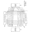
- the conventional AC surface-discharge PDP includes a PDP 30 arranged in a matrix type such that mxn discharge cells are connected to scan electrode lines Y1 to Ym, sustain electrode lines Z1 to Zm and address electrode lines X1 to Xn, a scan driver 32 for driving the scan electrode lines Y1 to Ym, a sustain driver 34 for driving the sustain electrode lines Z1 to Zm, and first and second address drivers 36A and 36B for making a divisional driving of odd-numbered address electrode lines X1, X3, ..., Xn-3, Xn-1 and even-numbered address electrode lines X2, X4, ..., Xn-2, Xn.
- the scan driver 32 sequentially applies a scan pulse and a sustain pulse to the scan electrode lines Y1 to Ym, to thereby sequentially scan discharge cells 1 for each line and sustain a discharge at each of the mxn discharge cells 1.
- the sustain driver 34 applies a sustain pulse to all the sustain electrode lines Z1 to Zm.
- the first and second address drivers 36A and 36M apply image data to the address electrode lines X1 to Xn in such a manner to be synchronized with a scan pulse.
- the first address driver 36A applies image data to the odd-numbered address electrode lines X1, X3, ..., Xn-3, Xn-1 while applying image data to the even-numbered address electrode lines X2, X4, ..., Xn-2, Xn.
- the AC surface-discharge PDP driven as mentioned above requires a high voltage more than hundreds of volts for an address discharge and a sustain discharge. Accordingly, in order to minimize a driving power required for the address discharge and the sustain discharge, the scan driver 32 and the sustain driver is additionally provided with an energy recovering apparatus 38 as shown in Fig. 3.
- the energy recovering apparatus 38 recovers a voltage charged in the scan electrode line Y and the sustain electrode line Z and re-uses the recovered voltage as a driving voltage for the next discharge.
- Such a conventional driving apparatus 38 includes an inductor L connected between a panel capacitor Cp and a source capacitor Cs, and first and third switches S1 and S3 connected, in parallel, between the source capacitor Cs and the inductor L.
- a scan/sustain driver 32 is comprised of second and fourth switches S2 and S4 connected, in parallel, between the panel capacitor Cp and the inductor L.
- the panel capacitor Cp is an equivalent expression of a capacitance formed between the scan electrode line Y and the sustain electrode line Z.
- the second switch S2 is connected to a sustain voltage source Vsus while the fourth switch S4 is connected to a ground voltage source GND.
- the source capacitor Cs recovers and charges a voltage charged in the panel capacitor Cp upon sustain discharge and re-supply the charged voltage to the panel capacitor Cp.
- the source capacitor Cs has a large capacitance value such that it can charge a voltage Vsus/2 equal to a half value of the sustain voltage Vsus.
- the first to fourth switches S1 to S4 controls a flow of current.
- the energy recovering apparatus 38 provided at the sustain driver 34 are formed around the panel capacitor Cp symmetrically with the scan driver 32.
- Fig. 4 is a timing diagram and a waveform diagram representing on/off timings of the switches shown in Fig. 3 and an output waveform of the panel capacitor.
- a voltage charged between the scan electrode line Y and the sustain electrode line Z that is, a voltage charged in the panel capacitor Cp prior to the T1 period should be 0 volt, and a voltage Vsus/2 has been charged in the source capacitor Cs.
- the first switch S1 is turned on, to thereby form a current path extending from the source capacitor Cs, via the first switch S1 and the inductor L, into the panel capacitor Cp.
- the inductor L and the panel capacitor L forms a serial resonance circuit. Since a voltage Vsus/2 has been charged in the source capacitor Cs, a voltage of the panel capacitor Cp rises into a sustain voltage Vsus equal to twice the voltage of the source capacitor Cs with the aid of a current charge/discharge of the inductor L in the serial resonance circuit.
- the second switch S2 is turned on to thereby apply the sustain voltage Vsus to the scan electrode line Y.
- the sustain voltage Vsus applied to the scan electrode line Y prevents a voltage of the panel capacitor Cp from falling into less than the sustain voltage Vsus to thereby cause a normal sustain discharge. Since a voltage of the panel capacitor Cp has risen into the sustain voltage Vsus in the T1 period, a driving power supplied from the exterior for the purposing of causing the sustain discharge is minimized.
- the first switch S1 is turned off and the panel capacitor Cp keeps the sustain voltage Vsus.
- the second switch S2 is turned off while the third switch S3 is turned on. If the third switch S3 is turned on, then a current path extending from the panel capacitor Cp, via the inductor L and the third switch S3, into the source capacitor Cs is formed to thereby recover a voltage charged in the panel capacitor Cp into the source capacitor Cs. While the panel capacitor Cp is discharged, a voltage of the panel capacitor Cp falls. At the same time, a voltage Vsus/2 is charged in the source capacitor Cs.
- the third switch S3 is turned off while the fourth switch S4 is turned on.
- the fourth switch S4 is turned on, a current path extending from the panel capacitor Cp into the ground voltage source GND, thereby allowing a voltage of the panel capacitor Cp to falls into 0 volt.
- the T6 period a state in the T5 period is kept for a certain time as it is.
- An AC driving pulse applied to the scan electrode line Y and the sustain electrode line Z is obtained by periodically repeating an operation procedure in the T1 to T6 periods.
- the scan electrode lines Y of the PDP driven in this manner are supplied with a sustain pulse in the sustain period, and are additionally supplied with a reset pulse and a scan pulse in the initialization period and the address period, respectively.
- the scan driver 32 is provided with a plurality of scan drive integrated circuits and a plurality of high-voltage switches.
- the sustain electrode line Z is directly connected to the sustain driver 34.
- a resistance of the current path at the scan driver 32 and the scan electrode line Y becomes larger than that of the current path at the sustain driver 34 and the sustain electrode line Z.
- the scan driver 32 has a smaller current supply capability than the sustain driver 34.
- pulse widths TP1 and TP2 of a first sustain pulse SUS1 and a second sustain pulse SUS2 applied to the scan electrode line Y and the sustain electrode line Z during the sustain period, respectively are equal to each other as shown in Fig. 5.
- a rising edge Tr1 of the first sustain pulse SUS1 is identical to a rising edge Tr2 of the second sustain pulse SUS2
- a falling edge Tf1 of the first sustain pulse SUS1 is identical to a falling edge of Tf2 of the second sustain pulse SUS2.
- the rising edges Tr1 and Tr2 of the first and second sustain pulses are time intervals going from an operation time of the energy recovering apparatus 38 shown in Fig. 3 until a turning-on time of the second switch S2 while the falling edges Tf1 and Tf2 thereof are time intervals going from an operation time of the energy recovering apparatus 38 into the fourth switch S4.
- intensities of sustain discharges caused by the first and second sustain pulses SUS1 and SUS2 applied to the scan electrode line Y and the sustain electrode line Z, respectively are differentiated to raises problems of an irregular discharge and hence a deterioration of picture quality.
- problems become more serious when a width of each of the first and second sustain pulses SUS1 and SUS2 is approximately 2 ⁇ s as a resolution is larger.
- a method of driving a plasma display panel having first and second row electrodes and a heat electrode and including a sustain period for implementing a gray scale depending upon a discharge frequency, includes the step of alternately applying first and second sustain pulses having a different width during the sustain period to the first and second row electrodes.
- a resistance going from a first driver generating the first sustain pulse into the first row electrode is different from a resistance going from a second driver generating the second sustain pulse into the second row electrode.
- said resistance going the first driver into the first row electrode is larger than a resistance going the second driver into the second row electrode.
- a width of the first sustain pulse may be longer than that of the second sustain pulse.
- a sustain period of the first sustain pulse may be longer than that of the second sustain pulse.
- a rising edge caused by an energy recovering circuit of the first sustain pulse may be shorter than a rising edge caused by the energy recovering circuit of the second sustain pulse.
- a resistance going from the second driver into the second row electrode may be larger than a resistance going from the first driver into the first row electrode.
- a width of the second sustain pulse may be longer than that of the first sustain pulse.
- a sustain period of the second sustain pulse may be longer than that of the first sustain pulse.
- a rising edge caused by an energy recovering circuit of the second sustain pulse may be shorter than a rising edge caused by the energy recovering circuit of the first sustain pulse.
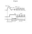
- Fig. 6 shows a method of driving a plasma display panel according to an embodiment of the present invention.
- each sub-field is divided into an initialization period for initializing cells of the entire field, and a sustain period for implementing a gray scale depending upon an address period for selecting a discharge cell and a discharge frequency.
- a rising ramp waveform Ramp-up generated at the scan driver is simultaneously applied to all the scan electrodes.
- the rising ramp waveform Ramp-up causes a weak discharge within cells of the entire field to thereby generate wall charges within the cells.
- a falling ramp waveform Ramp-down is simultaneously applied to the scan electrodes Y.
- the falling ramp waveform Ramp-down causes a weak erasure discharge with the cells, to thereby uniformly left wall charges required for the address discharge within the cells of the entire field.
- a negative scan pulse Scan is sequentially applied to the scan electrodes Y and, at the same time, a positive data pulse data is applied to the address electrodes X.
- An address discharge is generated within the cells to which the scan pulse Scan and the data pulse data are applied. Wall charges are generated within the cells selected by the address discharge.
- a positive direct current (DC) voltage zdc is applied to the sustain electrodes Z in the set-down period and the address period.
- the first and second sustain pulses SUS1 and SUS2 are alternately applied to the scan electrodes Y and the sustain electrodes Z.
- the cell selected by the address discharge causes a sustain discharge taking a surface-discharge type between the scan electrode Y and the sustain electrode Z whenever each of the sustain pulses SUS1 and SUS2 is applied while the wall charges within the cell being added to the sustain pulses SUS1 and SUS2.
- Widths of the first and second sustain pulses SUS1 and SUS2 applied to the scan electrode Y and the sustain electrode Z, respectively are differentiated. This will be described in detail with reference to Fig. 7A to Fig. 8B.
- Fig. 7A and Fig. 7B show a sustain pulse applied when a resistance of the current path extending from the scan driver into the scan electrode line Y is smaller than that of the current path extending from the sustain driver into the sustain electrode line Z.
- a width TP1 of the first sustain pulse SUS1 applied to the scan/sustain electrode line Y is smaller than a width TP2 of the second sustain pulse SUS2 applied to the sustain electrode line Z.
- a rising edge Tr1 of the first sustain pulse SUS1 is identical to a rising edge Tr2 of the second sustain pulse SUS2; a sustain interval Ts1 of the first sustain pulse SUS1 is shorter than a sustain interval Ts2 of the second sustain pulse SUS2; and a falling edge Tf1 of the first sustain pulse SUS1 is identical to a falling edge Tf2 of the second sustain pulse SUS2.
- a rising edge Tr1 of the first sustain pulse SUS1 is longer than to a rising edge Tr2 of the second sustain pulse SUS2; a sustain interval Ts1 of the first sustain pulse SUS1 is shorter than a sustain interval Ts2 of the second sustain pulse SUS2; and a falling edge Tf1 of the first sustain pulse SUS1 is identical to a falling edge Tf2 of the second sustain pulse SUS2.
- a rising edge of the sustain pulse is smaller, a discharge intensity becomes relatively larger.
- the rising edge Tr2 of the second sustain pulse SUS2 shorter than the rising edge Tr1 of the first sustain pulse SUS1 cause relatively larger discharge intensity.
- the rising edges Tr1 and Tr2 mean time intervals going from an operation time of the energy recovering circuit shown in Fig. 3 until an turning-on time of the second switch S2.
- the second sustain pulse SUS2 having a larger pulse width than the first sustain pulse SUS1 compensates for a resistance of the current path extending from the sustain driver into the sustain electrode line Z.
- a sustain discharge intensity between the scan electrode line Y and the sustain electrode line Z becomes equal. If the discharge intensity is equal, then a discharge becomes uniform to thereby improve a picture quality.
- a width TP1 of the first sustain pulse SUS1 applied to the scan/sustain electrode line Y is larger than a width TP2 of the second sustain pulse SUS2 applied to the sustain electrode line Z.
- a rising edge Tr1 of the first sustain pulse SUS1 is identical to a rising edge Tr2 of the second sustain pulse SUS2; a sustain interval Ts1 of the first sustain pulse SUS1 is longer than a sustain interval Ts2 of the second sustain pulse SUS2; and a falling edge Tf1 of the first sustain pulse SUS1 is identical to a falling edge Tf2 of the second sustain pulse SUS2.
- a rising edge Tr1 of the first sustain pulse SUS1 is shorter than to a rising edge Tr2 of the second sustain pulse SUS2; a sustain interval Ts1 of the first sustain pulse SUS1 is longer than a sustain interval Ts2 of the second sustain pulse SUS2; and a falling edge Tf1 of the first sustain pulse SUS1 is identical to a falling edge Tf2 of the second sustain pulse SUS2.
- a rising edge of the sustain pulse is smaller, a discharge intensity becomes relatively larger.
- the rising edge Tr1 of the first sustain pulse SUS1 shorter than the rising edge Tr2 of the second sustain pulse SUS2 cause relatively larger discharge intensity.
- the first sustain pulse SUS1 having a larger pulse width than the second sustain pulse SUS2 compensates for a resistance of the current path extending from the scan driver into the scan electrode line Y.
- a sustain discharge intensity between the scan electrode line Y and the sustain electrode line Z becomes equal. If the discharge intensity is equal, then a discharge becomes uniform to thereby improve a picture quality.
- a method of driving the plasma display panel embodying the present invention differentiates rising edges and sustain intervals of the first and second sustain pulses, thereby allowing the widths of the first and second sustain pulses to be different from each other.
- a sustain pulse having a relatively larger pulse width is applied to the electrode line having a relatively larger resistance of the current path extending from the electrode line into the driver. Accordingly, the sustain discharge intensity between the scan electrode and the sustain electrode is equal, so that it becomes possible to prevent an excessive discharge and hence improve a driving voltage margin.
Landscapes
- Engineering & Computer Science (AREA)
- Physics & Mathematics (AREA)
- Power Engineering (AREA)
- Plasma & Fusion (AREA)
- Computer Hardware Design (AREA)
- General Physics & Mathematics (AREA)
- Theoretical Computer Science (AREA)
- Control Of Indicators Other Than Cathode Ray Tubes (AREA)
- Control Of Gas Discharge Display Tubes (AREA)
Abstract
Description
- This invention relates to a plasma display panel, and more particularly to a method of driving a plasma display panel for improving a picture quality.
- Generally, a plasma display panel (PDP) uses ultraviolet rays, generated upon discharge of an inactive mixture gas such as He+Xe, Ne+Xe or He+Ne+Xe, to excite phosphorus material which then re-emits photons, to thereby display a picture. Such a PDP is easy to manufacture in thin-film and large-dimension formats. Moreover, such PDPs provide increasingly better picture quality owing to recent technical developments.
- Fig. 1 is a perspective view showing the structure of a conventional alternating current (AC) surface-discharge PDP.
- Referring to Fig. 1, a discharge cell of the conventional three-electrode, AC surface-discharge PDP includes a
scan electrode 12Y and asustain electrode 12Z provided on anupper substrate 10, and anaddress electrode 20X provided on alower substrate 18. - On the
upper substrate 10 provided with thescan electrode 12Y and thesustain electrode 12Z in parallel, an upperdielectric layer 14 and aprotective film 16 are disposed. Wall charges generated upon plasma discharge are accumulated into the upperdielectric layer 14. Theprotective film 16 prevents a damage of the upperdielectric layer 14 caused by a sputtering during the plasma discharge and improves the emission efficiency of secondary electrons. Thisprotective film 16 is usually made from magnesium oxide (MgO). - A lower
dielectric layer 22 andbarrier ribs 24 are formed on thelower substrate 18 provided with theaddress electrode 20X. The surfaces of the lowerdielectric layer 22 and thebarrier ribs 24 are coated with aphosphorous material 26. Theaddress electrode 20X is formed in a direction crossing thescan electrode 12Y and thesustain electrode 12Z. Thebarrier rib 24 is formed in parallel to theaddress electrode 20X to thereby prevent an ultraviolet ray and a visible light generated by a discharge from being leaked to the adjacent discharge cells. Thephosphorous material 26 is excited by an ultraviolet ray generated during the plasma discharge to generate any one of red, green and blue visible light rays. An inactive gas for a gas discharge is injected into a discharge space defined between the upper andlower substrate barrier rib 24. - Referring to Fig. 2, the conventional AC surface-discharge PDP includes a
PDP 30 arranged in a matrix type such that mxn discharge cells are connected to scan electrode lines Y1 to Ym, sustain electrode lines Z1 to Zm and address electrode lines X1 to Xn, ascan driver 32 for driving the scan electrode lines Y1 to Ym, asustain driver 34 for driving the sustain electrode lines Z1 to Zm, and first andsecond address drivers scan driver 32 sequentially applies a scan pulse and a sustain pulse to the scan electrode lines Y1 to Ym, to thereby sequentially scandischarge cells 1 for each line and sustain a discharge at each of themxn discharge cells 1. Thesustain driver 34 applies a sustain pulse to all the sustain electrode lines Z1 to Zm. The first andsecond address drivers 36A and 36M apply image data to the address electrode lines X1 to Xn in such a manner to be synchronized with a scan pulse. Thefirst address driver 36A applies image data to the odd-numbered address electrode lines X1, X3, ..., Xn-3, Xn-1 while applying image data to the even-numbered address electrode lines X2, X4, ..., Xn-2, Xn. - The AC surface-discharge PDP driven as mentioned above requires a high voltage more than hundreds of volts for an address discharge and a sustain discharge. Accordingly, in order to minimize a driving power required for the address discharge and the sustain discharge, the
scan driver 32 and the sustain driver is additionally provided with anenergy recovering apparatus 38 as shown in Fig. 3. Theenergy recovering apparatus 38 recovers a voltage charged in the scan electrode line Y and the sustain electrode line Z and re-uses the recovered voltage as a driving voltage for the next discharge. - Such a
conventional driving apparatus 38 includes an inductor L connected between a panel capacitor Cp and a source capacitor Cs, and first and third switches S1 and S3 connected, in parallel, between the source capacitor Cs and the inductor L. A scan/sustain driver 32 is comprised of second and fourth switches S2 and S4 connected, in parallel, between the panel capacitor Cp and the inductor L. The panel capacitor Cp is an equivalent expression of a capacitance formed between the scan electrode line Y and the sustain electrode line Z. The second switch S2 is connected to a sustain voltage source Vsus while the fourth switch S4 is connected to a ground voltage source GND. The source capacitor Cs recovers and charges a voltage charged in the panel capacitor Cp upon sustain discharge and re-supply the charged voltage to the panel capacitor Cp. The source capacitor Cs has a large capacitance value such that it can charge a voltage Vsus/2 equal to a half value of the sustain voltage Vsus. The first to fourth switches S1 to S4 controls a flow of current. Theenergy recovering apparatus 38 provided at thesustain driver 34 are formed around the panel capacitor Cp symmetrically with thescan driver 32. - Fig. 4 is a timing diagram and a waveform diagram representing on/off timings of the switches shown in Fig. 3 and an output waveform of the panel capacitor.
- An operation procedure of the
energy recovering apparatus 38 shown in Fig. 3 will be described in conjunction with Fig. 4. - First, it is assumed that a voltage charged between the scan electrode line Y and the sustain electrode line Z, that is, a voltage charged in the panel capacitor Cp prior to the T1 period should be 0 volt, and a voltage Vsus/2 has been charged in the source capacitor Cs.
- In the T1 period, the first switch S1 is turned on, to thereby form a current path extending from the source capacitor Cs, via the first switch S1 and the inductor L, into the panel capacitor Cp. At this time, the inductor L and the panel capacitor L forms a serial resonance circuit. Since a voltage Vsus/2 has been charged in the source capacitor Cs, a voltage of the panel capacitor Cp rises into a sustain voltage Vsus equal to twice the voltage of the source capacitor Cs with the aid of a current charge/discharge of the inductor L in the serial resonance circuit.
- In the T2 period, the second switch S2 is turned on to thereby apply the sustain voltage Vsus to the scan electrode line Y. The sustain voltage Vsus applied to the scan electrode line Y prevents a voltage of the panel capacitor Cp from falling into less than the sustain voltage Vsus to thereby cause a normal sustain discharge. Since a voltage of the panel capacitor Cp has risen into the sustain voltage Vsus in the T1 period, a driving power supplied from the exterior for the purposing of causing the sustain discharge is minimized.
- In the T3 period, the first switch S1 is turned off and the panel capacitor Cp keeps the sustain voltage Vsus. In the T4 period, the second switch S2 is turned off while the third switch S3 is turned on. If the third switch S3 is turned on, then a current path extending from the panel capacitor Cp, via the inductor L and the third switch S3, into the source capacitor Cs is formed to thereby recover a voltage charged in the panel capacitor Cp into the source capacitor Cs. While the panel capacitor Cp is discharged, a voltage of the panel capacitor Cp falls. At the same time, a voltage Vsus/2 is charged in the source capacitor Cs. After a voltage Vsus/2 was charged in the source capacitor Cs, the third switch S3 is turned off while the fourth switch S4 is turned on. In the fifth period when the fourth switch S4 is turned on, a current path extending from the panel capacitor Cp into the ground voltage source GND, thereby allowing a voltage of the panel capacitor Cp to falls into 0 volt. In the T6 period, a state in the T5 period is kept for a certain time as it is. An AC driving pulse applied to the scan electrode line Y and the sustain electrode line Z is obtained by periodically repeating an operation procedure in the T1 to T6 periods.
- The scan electrode lines Y of the PDP driven in this manner are supplied with a sustain pulse in the sustain period, and are additionally supplied with a reset pulse and a scan pulse in the initialization period and the address period, respectively. Accordingly, the
scan driver 32 is provided with a plurality of scan drive integrated circuits and a plurality of high-voltage switches. On the other hand, since the sustain pulse only is supplied, the sustain electrode line Z is directly connected to thesustain driver 34. As a result, a resistance of the current path at thescan driver 32 and the scan electrode line Y becomes larger than that of the current path at thesustain driver 34 and the sustain electrode line Z. Further, thescan driver 32 has a smaller current supply capability than thesustain driver 34. - In spite of such a resistance different of the current path and such a difference in the current supply capability, pulse widths TP1 and TP2 of a first sustain pulse SUS1 and a second sustain pulse SUS2 applied to the scan electrode line Y and the sustain electrode line Z during the sustain period, respectively are equal to each other as shown in Fig. 5. In other words, a rising edge Tr1 of the first sustain pulse SUS1 is identical to a rising edge Tr2 of the second sustain pulse SUS2, and a falling edge Tf1 of the first sustain pulse SUS1 is identical to a falling edge of Tf2 of the second sustain pulse SUS2. Herein, the rising edges Tr1 and Tr2 of the first and second sustain pulses are time intervals going from an operation time of the
energy recovering apparatus 38 shown in Fig. 3 until a turning-on time of the second switch S2 while the falling edges Tf1 and Tf2 thereof are time intervals going from an operation time of theenergy recovering apparatus 38 into the fourth switch S4. - Accordingly, intensities of sustain discharges caused by the first and second sustain pulses SUS1 and SUS2 applied to the scan electrode line Y and the sustain electrode line Z, respectively are differentiated to raises problems of an irregular discharge and hence a deterioration of picture quality. Particularly, such problems become more serious when a width of each of the first and second sustain pulses SUS1 and SUS2 is approximately 2µs as a resolution is larger.
- Accordingly, it would be desirable to provide a method of driving a plasma display panel which improves picture quality.
- In order to achieve these and other objects of the invention, a method of driving a plasma display panel according to an embodiment of the present invention, having first and second row electrodes and a heat electrode and including a sustain period for implementing a gray scale depending upon a discharge frequency, includes the step of alternately applying first and second sustain pulses having a different width during the sustain period to the first and second row electrodes.
- Preferably, a resistance going from a first driver generating the first sustain pulse into the first row electrode is different from a resistance going from a second driver generating the second sustain pulse into the second row electrode.
- Preferably, said resistance going the first driver into the first row electrode is larger than a resistance going the second driver into the second row electrode.
- A width of the first sustain pulse may be longer than that of the second sustain pulse.
- A sustain period of the first sustain pulse may be longer than that of the second sustain pulse.
- A rising edge caused by an energy recovering circuit of the first sustain pulse may be shorter than a rising edge caused by the energy recovering circuit of the second sustain pulse.
- Alternatively, a resistance going from the second driver into the second row electrode may be larger than a resistance going from the first driver into the first row electrode.
- A width of the second sustain pulse may be longer than that of the first sustain pulse.
- A sustain period of the second sustain pulse may be longer than that of the first sustain pulse.
- A rising edge caused by an energy recovering circuit of the second sustain pulse may be shorter than a rising edge caused by the energy recovering circuit of the first sustain pulse.
- These and other objects of the invention will be apparent from the following detailed description of the embodiments of the present invention with reference to the accompanying drawings, in which:
- Fig. 1 is a perspective view representing a structure of a conventional AC surface-discharge plasma display panel;
- Fig. 2 is a plan view showing an arrangement structure of overall electrode lines and discharge cells of the plasma display panel in Fig. 1;
- Fig. 3 is a circuit diagram of a conventional energy recovering apparatus provided at the pre-stage of the sustain driver in Fig. 2;
- Fig. 4 is a timing diagram and a waveform diagram representing an ON/OFF timing of each switch shown in Fig. 2 and an output waveform of the panel capacitor;
- Fig. 5 is a detailed waveform diagram of a sustain pulse applied to the sustain electrode pair shown in Fig. 2;
- Fig. 6 is a waveform diagram for explaining a method of driving a plasma display panel according to an embodiment of the present invention;
- Fig. 7A and Fig. 7B are detailed waveform diagrams of the first and second sustain pulses in the sustain period shown in Fig. 6; and
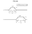
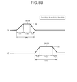
- Fig. 8A and Fig. 8B are detailed waveform diagrams showing another shapes of the first and second sustain pulses in the sustain period shown in Fig. 6.
-
- Fig. 6 shows a method of driving a plasma display panel according to an embodiment of the present invention.
- Referring to Fig. 6, each sub-field is divided into an initialization period for initializing cells of the entire field, and a sustain period for implementing a gray scale depending upon an address period for selecting a discharge cell and a discharge frequency.
- In the initialization period, a rising ramp waveform Ramp-up generated at the scan driver is simultaneously applied to all the scan electrodes. The rising ramp waveform Ramp-up causes a weak discharge within cells of the entire field to thereby generate wall charges within the cells. After the rising ramp waveform Ramp-up was applied, a falling ramp waveform Ramp-down is simultaneously applied to the scan electrodes Y. The falling ramp waveform Ramp-down causes a weak erasure discharge with the cells, to thereby uniformly left wall charges required for the address discharge within the cells of the entire field.
- In the address period, a negative scan pulse Scan is sequentially applied to the scan electrodes Y and, at the same time, a positive data pulse data is applied to the address electrodes X. An address discharge is generated within the cells to which the scan pulse Scan and the data pulse data are applied. Wall charges are generated within the cells selected by the address discharge. A positive direct current (DC) voltage zdc is applied to the sustain electrodes Z in the set-down period and the address period.
- In the sustain period, the first and second sustain pulses SUS1 and SUS2 are alternately applied to the scan electrodes Y and the sustain electrodes Z. The cell selected by the address discharge causes a sustain discharge taking a surface-discharge type between the scan electrode Y and the sustain electrode Z whenever each of the sustain pulses SUS1 and SUS2 is applied while the wall charges within the cell being added to the sustain pulses SUS1 and SUS2.
- Widths of the first and second sustain pulses SUS1 and SUS2 applied to the scan electrode Y and the sustain electrode Z, respectively are differentiated. This will be described in detail with reference to Fig. 7A to Fig. 8B.
- Fig. 7A and Fig. 7B show a sustain pulse applied when a resistance of the current path extending from the scan driver into the scan electrode line Y is smaller than that of the current path extending from the sustain driver into the sustain electrode line Z.
- Referring to Fig. 8A and Fig. 8B, a width TP1 of the first sustain pulse SUS1 applied to the scan/sustain electrode line Y is smaller than a width TP2 of the second sustain pulse SUS2 applied to the sustain electrode line Z.
- As shown in Fig. 8A, a rising edge Tr1 of the first sustain pulse SUS1 is identical to a rising edge Tr2 of the second sustain pulse SUS2; a sustain interval Ts1 of the first sustain pulse SUS1 is shorter than a sustain interval Ts2 of the second sustain pulse SUS2; and a falling edge Tf1 of the first sustain pulse SUS1 is identical to a falling edge Tf2 of the second sustain pulse SUS2.
- As shown in Fig. 8B, a rising edge Tr1 of the first sustain pulse SUS1 is longer than to a rising edge Tr2 of the second sustain pulse SUS2; a sustain interval Ts1 of the first sustain pulse SUS1 is shorter than a sustain interval Ts2 of the second sustain pulse SUS2; and a falling edge Tf1 of the first sustain pulse SUS1 is identical to a falling edge Tf2 of the second sustain pulse SUS2. As a rising edge of the sustain pulse is smaller, a discharge intensity becomes relatively larger. The rising edge Tr2 of the second sustain pulse SUS2 shorter than the rising edge Tr1 of the first sustain pulse SUS1 cause relatively larger discharge intensity. Herein, the rising edges Tr1 and Tr2 mean time intervals going from an operation time of the energy recovering circuit shown in Fig. 3 until an turning-on time of the second switch S2.
- Accordingly, the second sustain pulse SUS2 having a larger pulse width than the first sustain pulse SUS1 compensates for a resistance of the current path extending from the sustain driver into the sustain electrode line Z. Thus, a sustain discharge intensity between the scan electrode line Y and the sustain electrode line Z becomes equal. If the discharge intensity is equal, then a discharge becomes uniform to thereby improve a picture quality.
- Referring to Fig. 7A and Fig. 7B, a width TP1 of the first sustain pulse SUS1 applied to the scan/sustain electrode line Y is larger than a width TP2 of the second sustain pulse SUS2 applied to the sustain electrode line Z.
- As shown in Fig. 7A, a rising edge Tr1 of the first sustain pulse SUS1 is identical to a rising edge Tr2 of the second sustain pulse SUS2; a sustain interval Ts1 of the first sustain pulse SUS1 is longer than a sustain interval Ts2 of the second sustain pulse SUS2; and a falling edge Tf1 of the first sustain pulse SUS1 is identical to a falling edge Tf2 of the second sustain pulse SUS2.
- As shown in Fig. 7B, a rising edge Tr1 of the first sustain pulse SUS1 is shorter than to a rising edge Tr2 of the second sustain pulse SUS2; a sustain interval Ts1 of the first sustain pulse SUS1 is longer than a sustain interval Ts2 of the second sustain pulse SUS2; and a falling edge Tf1 of the first sustain pulse SUS1 is identical to a falling edge Tf2 of the second sustain pulse SUS2. As a rising edge of the sustain pulse is smaller, a discharge intensity becomes relatively larger. The rising edge Tr1 of the first sustain pulse SUS1 shorter than the rising edge Tr2 of the second sustain pulse SUS2 cause relatively larger discharge intensity.
- Accordingly, the first sustain pulse SUS1 having a larger pulse width than the second sustain pulse SUS2 compensates for a resistance of the current path extending from the scan driver into the scan electrode line Y. Thus, a sustain discharge intensity between the scan electrode line Y and the sustain electrode line Z becomes equal. If the discharge intensity is equal, then a discharge becomes uniform to thereby improve a picture quality.
- As described above, a method of driving the plasma display panel embodying the present invention differentiates rising edges and sustain intervals of the first and second sustain pulses, thereby allowing the widths of the first and second sustain pulses to be different from each other. In other words, a sustain pulse having a relatively larger pulse width is applied to the electrode line having a relatively larger resistance of the current path extending from the electrode line into the driver. Accordingly, the sustain discharge intensity between the scan electrode and the sustain electrode is equal, so that it becomes possible to prevent an excessive discharge and hence improve a driving voltage margin.
- Although the present invention has been explained by the embodiments shown in the drawings described above, it should be understood to the ordinary skilled person in the art that the invention is not limited to the embodiments, but rather that various changes or modifications thereof are possible without departing from the scope of the invention. Accordingly, the scope of the invention shall be determined only by the appended claims.
Claims (12)
- A method of driving a plasma display panel having first and second row electrodes and a heat electrode and including a sustain period for implementing a gray scale depending upon a discharge frequency, comprising the step of:alternately applying first and second sustain pulses having a different width during the sustain period to the first and second row electrodes.
- The method as claimed in claim 1, wherein a resistance going from a first driver generating the first sustain pulse into the first row electrode is different from a resistance going from a second driver generating the second sustain pulse into the second row electrode.
- The method as claimed in claim 2, wherein said resistance going the first driver into the first row electrode is larger than a resistance going the second driver into the second row electrode.
- The method as claimed in claim 3, wherein a width of the first sustain pulse is longer than that of the second sustain pulse.
- The method as claimed in claim 3, wherein a sustain period of the first sustain pulse is longer than that of the second sustain pulse.
- The method as claimed in claim 5, wherein a rising edge caused by an energy recovering circuit of the first sustain pulse is shorter than a rising edge caused by the energy recovering circuit of the second sustain pulse.
- The method as claimed in claim 2, wherein a resistance going from the second driver into the second row electrode is larger than a resistance going from the first driver into the first row electrode.
- The method as claimed in claim 7, wherein a width of the second sustain pulse is longer than that of the first sustain pulse.
- The method as claimed in claim 7, wherein a sustain period of the second sustain pulse is longer than that of the first sustain pulse.
- The method as claimed in claim 9, wherein a rising edge caused by an energy recovering circuit of the second sustain pulse is shorter than a rising edge caused by the energy recovering circuit of the first sustain pulse.
- A plasma display panel having first and second row electrodes and a heat electrode and including a sustain period for implementing a gray scale depending upon a discharge frequency, further adapted to alternatively apply first and second sustain pulses having a different width during the sustain period to the first and second row electrodes.
- Apparatus adapted to carry out the method steps of any of claims 1 to 10.
Applications Claiming Priority (2)
| Application Number | Priority Date | Filing Date | Title |
|---|---|---|---|
| KR10-2002-0045605A KR100472372B1 (en) | 2002-08-01 | 2002-08-01 | Method Of Driving Plasma Display Panel |
| KR2002045605 | 2002-08-01 |
Publications (2)
| Publication Number | Publication Date |
|---|---|
| EP1387345A2 true EP1387345A2 (en) | 2004-02-04 |
| EP1387345A3 EP1387345A3 (en) | 2006-01-11 |
Family
ID=30113216
Family Applications (1)
| Application Number | Title | Priority Date | Filing Date |
|---|---|---|---|
| EP03254808A Withdrawn EP1387345A3 (en) | 2002-08-01 | 2003-07-31 | Method of driving a plasma display panel |
Country Status (3)
| Country | Link |
|---|---|
| US (3) | US7187346B2 (en) |
| EP (1) | EP1387345A3 (en) |
| KR (1) | KR100472372B1 (en) |
Cited By (5)
| Publication number | Priority date | Publication date | Assignee | Title |
|---|---|---|---|---|
| EP1727118A2 (en) | 2005-05-23 | 2006-11-29 | Lg Electronics Inc. | Plasma display driving apparatus and driving method |
| EP1760685A3 (en) * | 2005-09-06 | 2008-06-11 | LG Electronics Inc. | Plasma display apparatus |
| EP1936592A3 (en) * | 2006-12-19 | 2009-03-11 | LG Electronics Inc. | Plasma display apparatus and method of driving the same |
| EP1923856A4 (en) * | 2006-07-11 | 2010-01-20 | Panasonic Corp | PLASMA SCREEN AND METHOD FOR CONTROLLING ITS DISPLAY PANEL |
| EP1679685A3 (en) * | 2005-01-10 | 2010-04-21 | LG Electronics Inc. | Sustain pulse controlling method and apparatus for a plasma display apparatus |
Families Citing this family (31)
| Publication number | Priority date | Publication date | Assignee | Title |
|---|---|---|---|---|
| KR100550983B1 (en) * | 2003-11-26 | 2006-02-13 | 삼성에스디아이 주식회사 | Driving Method of Plasma Display and Plasma Display Panel |
| KR100542227B1 (en) * | 2004-03-10 | 2006-01-10 | 삼성에스디아이 주식회사 | Driving device and driving method of plasma display panel |
| JP4647220B2 (en) * | 2004-03-24 | 2011-03-09 | 日立プラズマディスプレイ株式会社 | Driving method of plasma display device |
| JP4443998B2 (en) * | 2004-05-24 | 2010-03-31 | パナソニック株式会社 | Driving method of plasma display panel |
| KR100542772B1 (en) * | 2004-07-16 | 2006-01-20 | 엘지전자 주식회사 | Plasma display panel driving method and apparatus |
| US20060033680A1 (en) * | 2004-08-11 | 2006-02-16 | Lg Electronics Inc. | Plasma display apparatus including an energy recovery circuit |
| KR100551041B1 (en) * | 2004-08-12 | 2006-02-13 | 삼성에스디아이 주식회사 | Driving Method of Plasma Display Panel and Plasma Display Device |
| KR100590112B1 (en) * | 2004-11-16 | 2006-06-14 | 삼성에스디아이 주식회사 | Plasma display device and driving method thereof |
| KR100607259B1 (en) * | 2004-12-30 | 2006-08-01 | 엘지전자 주식회사 | Plasma Display Panel Driver |
| KR100603662B1 (en) * | 2005-01-06 | 2006-07-24 | 엘지전자 주식회사 | Driving apparatus and method of plasma display panel |
| JP2006195463A (en) * | 2005-01-10 | 2006-07-27 | Lg Electronics Inc | Plasma display apparatus |
| KR100666106B1 (en) * | 2005-07-16 | 2007-01-09 | 엘지전자 주식회사 | Plasma display device |
| KR100740150B1 (en) * | 2005-09-07 | 2007-07-16 | 엘지전자 주식회사 | Plasma display device |
| KR100726661B1 (en) * | 2005-09-28 | 2007-06-13 | 엘지전자 주식회사 | Plasma display |
| JPWO2007094291A1 (en) * | 2006-02-14 | 2009-07-09 | パナソニック株式会社 | Plasma display apparatus and driving method of plasma display panel |
| CN101351831B (en) * | 2006-02-14 | 2012-02-22 | 松下电器产业株式会社 | Plasma display device and plasma display panel drive method |
| KR100784527B1 (en) * | 2006-05-26 | 2007-12-11 | 엘지전자 주식회사 | Driving Method of Plasma Display Device |
| KR100784528B1 (en) * | 2006-05-26 | 2007-12-11 | 엘지전자 주식회사 | Driving Method of Plasma Display Device |
| CN101356568B (en) * | 2006-07-14 | 2011-12-14 | 松下电器产业株式会社 | Plasma display device and method for driving plasma display panel |
| KR100800499B1 (en) * | 2006-07-18 | 2008-02-04 | 엘지전자 주식회사 | Plasma display device |
| KR100811549B1 (en) | 2006-08-07 | 2008-03-07 | 엘지전자 주식회사 | Plasma display device |
| KR100800521B1 (en) * | 2006-08-10 | 2008-02-04 | 엘지전자 주식회사 | Plasma display device and driving method thereof |
| JP4374006B2 (en) * | 2006-09-01 | 2009-12-02 | 日立プラズマディスプレイ株式会社 | Plasma display panel driving method and plasma display apparatus |
| KR100811474B1 (en) * | 2006-10-27 | 2008-03-07 | 엘지전자 주식회사 | Plasma display device |
| KR100778456B1 (en) * | 2006-12-18 | 2007-11-21 | 삼성에스디아이 주식회사 | Plasma display device and driving method thereof |
| US20080150835A1 (en) * | 2006-12-20 | 2008-06-26 | Lg Electronics Inc. | Plasma display apparatus and driving method thereof |
| JPWO2008105160A1 (en) * | 2007-02-27 | 2010-06-03 | パナソニック株式会社 | Driving method of plasma display panel |
| KR101061703B1 (en) * | 2007-04-25 | 2011-09-01 | 파나소닉 주식회사 | Driving Method of Plasma Display Panel |
| KR20090017206A (en) | 2007-08-14 | 2009-02-18 | 엘지전자 주식회사 | Plasma Display Panel And Method Of Manufacturing The Same |
| US20120293469A1 (en) * | 2010-01-19 | 2012-11-22 | Hidehiko Shoji | Plasma display panel driving method and plasma display device |
| CN102714014A (en) * | 2010-01-19 | 2012-10-03 | 松下电器产业株式会社 | Plasma display panel driving method and plasma display device |
Family Cites Families (29)
| Publication number | Priority date | Publication date | Assignee | Title |
|---|---|---|---|---|
| JP2755201B2 (en) * | 1994-09-28 | 1998-05-20 | 日本電気株式会社 | Drive circuit for plasma display panel |
| JP3121247B2 (en) * | 1995-10-16 | 2000-12-25 | 富士通株式会社 | AC-type plasma display panel and driving method |
| US6188374B1 (en) * | 1997-03-28 | 2001-02-13 | Lg Electronics, Inc. | Plasma display panel and driving apparatus therefor |
| US6160530A (en) | 1997-04-02 | 2000-12-12 | Nec Corporation | Method and device for driving a plasma display panel |
| JP3897896B2 (en) * | 1997-07-16 | 2007-03-28 | 三菱電機株式会社 | Plasma display panel driving method and plasma display device |
| US6369781B2 (en) | 1997-10-03 | 2002-04-09 | Mitsubishi Denki Kabushiki Kaisha | Method of driving plasma display panel |
| JP2000047634A (en) | 1998-07-29 | 2000-02-18 | Pioneer Electron Corp | Driving method of plasma display device |
| JP2000047635A (en) * | 1998-07-29 | 2000-02-18 | Pioneer Electron Corp | Driving method of plasma display device |
| KR20000021115A (en) * | 1998-09-25 | 2000-04-15 | 구자홍 | Method for driving plasma display panel |
| JP3692827B2 (en) | 1999-04-20 | 2005-09-07 | 松下電器産業株式会社 | Driving method of AC type plasma display panel |
| KR20000073134A (en) * | 1999-05-06 | 2000-12-05 | 황기웅 | A method for driving a PDP |
| KR100335103B1 (en) * | 1999-08-09 | 2002-05-04 | 구자홍 | Structure and method for plasma display panel |
| JP2001228820A (en) * | 2000-02-14 | 2001-08-24 | Mitsubishi Electric Corp | Driving method of plasma display panel and plasma display device |
| JP3514205B2 (en) | 2000-03-10 | 2004-03-31 | 日本電気株式会社 | Driving method of plasma display panel |
| JP3644867B2 (en) * | 2000-03-29 | 2005-05-11 | 富士通日立プラズマディスプレイ株式会社 | Plasma display device and manufacturing method thereof |
| JP3765381B2 (en) * | 2000-05-25 | 2006-04-12 | パイオニア株式会社 | Plasma display device |
| JP2002072957A (en) | 2000-08-24 | 2002-03-12 | Matsushita Electric Ind Co Ltd | Driving method of plasma display panel |
| JP2002140033A (en) | 2000-11-02 | 2002-05-17 | Fujitsu Hitachi Plasma Display Ltd | Driving method for plasma display |
| JP2002162931A (en) * | 2000-11-24 | 2002-06-07 | Nec Corp | Driving method for plasma display panel |
| JP4606612B2 (en) | 2001-02-05 | 2011-01-05 | 日立プラズマディスプレイ株式会社 | Driving method of plasma display panel |
| DE10162258A1 (en) | 2001-03-23 | 2002-09-26 | Samsung Sdi Co | Operating plasma display involves inhibiting reset discharge in cells in which address discharge can occur in address interval, allowing reset discharge in cells without this characteristic |
| KR100381270B1 (en) * | 2001-05-10 | 2003-04-26 | 엘지전자 주식회사 | Method of Driving Plasma Display Panel |
| KR100400007B1 (en) | 2001-06-22 | 2003-09-29 | 삼성전자주식회사 | Apparatus and method for improving power recovery rate of a plasma display panel driver |
| JP3682422B2 (en) | 2001-06-26 | 2005-08-10 | 株式会社日立製作所 | Driving method of plasma display device |
| JP2003015595A (en) * | 2001-06-29 | 2003-01-17 | Pioneer Electronic Corp | Drive circuit for pdp display device |
| KR100428625B1 (en) | 2001-08-06 | 2004-04-27 | 삼성에스디아이 주식회사 | A scan electrode driving apparatus of an ac plasma display panel and the driving method thereof |
| KR100472505B1 (en) | 2001-11-14 | 2005-03-10 | 삼성에스디아이 주식회사 | Method and apparatus for driving plasma display panel which is operated with middle discharge mode in reset period |
| JP4299987B2 (en) | 2001-12-21 | 2009-07-22 | 株式会社日立製作所 | Plasma display device and driving method thereof |
| KR100467692B1 (en) * | 2002-04-18 | 2005-01-24 | 삼성에스디아이 주식회사 | Method of driving plasma display panel wherein width of display sustain pulse varies |
-
2002
- 2002-08-01 KR KR10-2002-0045605A patent/KR100472372B1/en not_active Expired - Fee Related
-
2003
- 2003-07-31 US US10/630,720 patent/US7187346B2/en not_active Expired - Fee Related
- 2003-07-31 EP EP03254808A patent/EP1387345A3/en not_active Withdrawn
-
2006
- 2006-12-14 US US11/638,585 patent/US7812790B2/en not_active Expired - Fee Related
- 2006-12-20 US US11/641,873 patent/US20070097051A1/en not_active Abandoned
Non-Patent Citations (1)
| Title |
|---|
| None |
Cited By (7)
| Publication number | Priority date | Publication date | Assignee | Title |
|---|---|---|---|---|
| EP1679685A3 (en) * | 2005-01-10 | 2010-04-21 | LG Electronics Inc. | Sustain pulse controlling method and apparatus for a plasma display apparatus |
| EP1727118A2 (en) | 2005-05-23 | 2006-11-29 | Lg Electronics Inc. | Plasma display driving apparatus and driving method |
| EP1727118A3 (en) * | 2005-05-23 | 2007-02-21 | Lg Electronics Inc. | Plasma display driving apparatus and driving method |
| EP1760685A3 (en) * | 2005-09-06 | 2008-06-11 | LG Electronics Inc. | Plasma display apparatus |
| EP1923856A4 (en) * | 2006-07-11 | 2010-01-20 | Panasonic Corp | PLASMA SCREEN AND METHOD FOR CONTROLLING ITS DISPLAY PANEL |
| EP1936592A3 (en) * | 2006-12-19 | 2009-03-11 | LG Electronics Inc. | Plasma display apparatus and method of driving the same |
| US7944408B2 (en) | 2006-12-19 | 2011-05-17 | Lg Electronics Inc. | Plasma display apparatus and method of driving the same |
Also Published As
| Publication number | Publication date |
|---|---|
| US20070091046A1 (en) | 2007-04-26 |
| US7187346B2 (en) | 2007-03-06 |
| US7812790B2 (en) | 2010-10-12 |
| KR20040013160A (en) | 2004-02-14 |
| US20040021657A1 (en) | 2004-02-05 |
| EP1387345A3 (en) | 2006-01-11 |
| US20070097051A1 (en) | 2007-05-03 |
| KR100472372B1 (en) | 2005-02-21 |
Similar Documents
| Publication | Publication Date | Title |
|---|---|---|
| EP1387345A2 (en) | Method of driving a plasma display panel | |
| US6504519B1 (en) | Plasma display panel and apparatus and method of driving the same | |
| CN100416631C (en) | Apparatus and method for driving plasma display panel | |
| KR100351466B1 (en) | Energy Recovery Apparatus in Plasma Display Panel | |
| US20060092102A1 (en) | Method of driving plasma display panel | |
| KR100330032B1 (en) | Energy Recovery Apparatus and Method of Addressing Cells using the same in Plasma Display Panel | |
| KR100426190B1 (en) | Apparatus and mehtod of driving plasma display panel | |
| EP1484739A2 (en) | Method for driving a three-electrode plasma display panel with application of DC voltage to address electrodes during the sustain period | |
| KR100493623B1 (en) | Apparatus For Driving Plasma Display Panel | |
| KR100499374B1 (en) | Apparatus and Method of Energy Recovery and Driving Method of Plasma Display Panel Using the same | |
| KR100341312B1 (en) | Method Of Driving Plasma Display Panel And Apparatus Thereof | |
| KR100582205B1 (en) | Driving Method of Plasma Display Panel | |
| US7692608B2 (en) | Energy recovery circuit and energy recovering method using the same | |
| KR100363675B1 (en) | Energy Recovery Apparatus and Method in Plasma Display Panel | |
| US20080266211A1 (en) | Plasma Display Panel, Plasma Display Device, and Method for Driving Plasma Display Panel | |
| KR100366943B1 (en) | Energy Recovery Apparatus in Plasma Display Panel and Driving Method Thereof | |
| EP1686558A2 (en) | Plasma display panel comprising energy recovery circuit and driving method thereof | |
| KR100467073B1 (en) | Methdo and apparatus driving of plasma display panel | |
| KR20020039706A (en) | Reset Circuit in Plasma Display Panel | |
| KR100373531B1 (en) | Energy Recovery Apparatus in Plasma Display Panel and Driving Method Thereof | |
| KR100336609B1 (en) | Method of Driving Plasma Display Panel | |
| KR100667109B1 (en) | Plasma Display Panel and Driving Method thereof | |
| EP1835480A1 (en) | Method of driving plasma display panel | |
| Wu et al. | Design and development of driving waveforms for AC PDPs | |
| KR100364398B1 (en) | Plasma Display Panel and Driving Method Thereof |
Legal Events
| Date | Code | Title | Description |
|---|---|---|---|
| PUAI | Public reference made under article 153(3) epc to a published international application that has entered the european phase |
Free format text: ORIGINAL CODE: 0009012 |
|
| AK | Designated contracting states |
Kind code of ref document: A2 Designated state(s): AT BE BG CH CY CZ DE DK EE ES FI FR GB GR HU IE IT LI LU MC NL PT RO SE SI SK TR |
|
| AX | Request for extension of the european patent |
Extension state: AL LT LV MK |
|
| RIN1 | Information on inventor provided before grant (corrected) |
Inventor name: YUN, SANG JIN#103-1802,WOOBANGSINCHEONJI TOWN Inventor name: KANG, SEONG HO |
|
| PUAL | Search report despatched |
Free format text: ORIGINAL CODE: 0009013 |
|
| AK | Designated contracting states |
Kind code of ref document: A3 Designated state(s): AT BE BG CH CY CZ DE DK EE ES FI FR GB GR HU IE IT LI LU MC NL PT RO SE SI SK TR |
|
| AX | Request for extension of the european patent |
Extension state: AL LT LV MK |
|
| 17P | Request for examination filed |
Effective date: 20060109 |
|
| AKX | Designation fees paid |
Designated state(s): AT BE BG CH CY CZ DE DK EE ES FI FR GB GR HU IE IT LI LU MC NL PT RO SE SI SK TR |
|
| 17Q | First examination report despatched |
Effective date: 20070207 |
|
| RIN1 | Information on inventor provided before grant (corrected) |
Inventor name: YUN, SANG JIN 103-1802,WOOBANGSINCHEONJI TOWN Inventor name: KANG, SEONG HO |
|
| RIC1 | Information provided on ipc code assigned before grant |
Ipc: G09G 3/294 20130101AFI20140805BHEP |
|
| GRAP | Despatch of communication of intention to grant a patent |
Free format text: ORIGINAL CODE: EPIDOSNIGR1 |
|
| INTG | Intention to grant announced |
Effective date: 20140912 |
|
| STAA | Information on the status of an ep patent application or granted ep patent |
Free format text: STATUS: THE APPLICATION IS DEEMED TO BE WITHDRAWN |
|
| 18D | Application deemed to be withdrawn |
Effective date: 20150203 |