EP1386376B1 - Laser spectral engineering for lithographic process - Google Patents
Laser spectral engineering for lithographic process Download PDFInfo
- Publication number
- EP1386376B1 EP1386376B1 EP02731433A EP02731433A EP1386376B1 EP 1386376 B1 EP1386376 B1 EP 1386376B1 EP 02731433 A EP02731433 A EP 02731433A EP 02731433 A EP02731433 A EP 02731433A EP 1386376 B1 EP1386376 B1 EP 1386376B1
- Authority
- EP
- European Patent Office
- Prior art keywords
- wavelength
- laser
- pulses
- spectrum
- bandwidth
- Prior art date
- Legal status (The legal status is an assumption and is not a legal conclusion. Google has not performed a legal analysis and makes no representation as to the accuracy of the status listed.)
- Expired - Lifetime
Links
Images


Classifications
-
- G—PHYSICS
- G03—PHOTOGRAPHY; CINEMATOGRAPHY; ANALOGOUS TECHNIQUES USING WAVES OTHER THAN OPTICAL WAVES; ELECTROGRAPHY; HOLOGRAPHY
- G03F—PHOTOMECHANICAL PRODUCTION OF TEXTURED OR PATTERNED SURFACES, e.g. FOR PRINTING, FOR PROCESSING OF SEMICONDUCTOR DEVICES; MATERIALS THEREFOR; ORIGINALS THEREFOR; APPARATUS SPECIALLY ADAPTED THEREFOR
- G03F7/00—Photomechanical, e.g. photolithographic, production of textured or patterned surfaces, e.g. printing surfaces; Materials therefor, e.g. comprising photoresists; Apparatus specially adapted therefor
- G03F7/70—Microphotolithographic exposure; Apparatus therefor
- G03F7/70008—Production of exposure light, i.e. light sources
- G03F7/70025—Production of exposure light, i.e. light sources by lasers
-
- G—PHYSICS
- G03—PHOTOGRAPHY; CINEMATOGRAPHY; ANALOGOUS TECHNIQUES USING WAVES OTHER THAN OPTICAL WAVES; ELECTROGRAPHY; HOLOGRAPHY
- G03F—PHOTOMECHANICAL PRODUCTION OF TEXTURED OR PATTERNED SURFACES, e.g. FOR PRINTING, FOR PROCESSING OF SEMICONDUCTOR DEVICES; MATERIALS THEREFOR; ORIGINALS THEREFOR; APPARATUS SPECIALLY ADAPTED THEREFOR
- G03F7/00—Photomechanical, e.g. photolithographic, production of textured or patterned surfaces, e.g. printing surfaces; Materials therefor, e.g. comprising photoresists; Apparatus specially adapted therefor
- G03F7/70—Microphotolithographic exposure; Apparatus therefor
- G03F7/70008—Production of exposure light, i.e. light sources
- G03F7/70041—Production of exposure light, i.e. light sources by pulsed sources, e.g. multiplexing, pulse duration, interval control or intensity control
-
- G—PHYSICS
- G03—PHOTOGRAPHY; CINEMATOGRAPHY; ANALOGOUS TECHNIQUES USING WAVES OTHER THAN OPTICAL WAVES; ELECTROGRAPHY; HOLOGRAPHY
- G03F—PHOTOMECHANICAL PRODUCTION OF TEXTURED OR PATTERNED SURFACES, e.g. FOR PRINTING, FOR PROCESSING OF SEMICONDUCTOR DEVICES; MATERIALS THEREFOR; ORIGINALS THEREFOR; APPARATUS SPECIALLY ADAPTED THEREFOR
- G03F7/00—Photomechanical, e.g. photolithographic, production of textured or patterned surfaces, e.g. printing surfaces; Materials therefor, e.g. comprising photoresists; Apparatus specially adapted therefor
- G03F7/70—Microphotolithographic exposure; Apparatus therefor
- G03F7/70216—Mask projection systems
- G03F7/70325—Resolution enhancement techniques not otherwise provided for, e.g. darkfield imaging, interfering beams, spatial frequency multiplication, nearfield lenses or solid immersion lenses
- G03F7/70333—Focus drilling, i.e. increase in depth of focus for exposure by modulating focus during exposure [FLEX]
-
- G—PHYSICS
- G03—PHOTOGRAPHY; CINEMATOGRAPHY; ANALOGOUS TECHNIQUES USING WAVES OTHER THAN OPTICAL WAVES; ELECTROGRAPHY; HOLOGRAPHY
- G03F—PHOTOMECHANICAL PRODUCTION OF TEXTURED OR PATTERNED SURFACES, e.g. FOR PRINTING, FOR PROCESSING OF SEMICONDUCTOR DEVICES; MATERIALS THEREFOR; ORIGINALS THEREFOR; APPARATUS SPECIALLY ADAPTED THEREFOR
- G03F7/00—Photomechanical, e.g. photolithographic, production of textured or patterned surfaces, e.g. printing surfaces; Materials therefor, e.g. comprising photoresists; Apparatus specially adapted therefor
- G03F7/70—Microphotolithographic exposure; Apparatus therefor
- G03F7/70483—Information management; Active and passive control; Testing; Wafer monitoring, e.g. pattern monitoring
- G03F7/7055—Exposure light control in all parts of the microlithographic apparatus, e.g. pulse length control or light interruption
- G03F7/70575—Wavelength control, e.g. control of bandwidth, multiple wavelength, selection of wavelength or matching of optical components to wavelength
-
- G—PHYSICS
- G03—PHOTOGRAPHY; CINEMATOGRAPHY; ANALOGOUS TECHNIQUES USING WAVES OTHER THAN OPTICAL WAVES; ELECTROGRAPHY; HOLOGRAPHY
- G03F—PHOTOMECHANICAL PRODUCTION OF TEXTURED OR PATTERNED SURFACES, e.g. FOR PRINTING, FOR PROCESSING OF SEMICONDUCTOR DEVICES; MATERIALS THEREFOR; ORIGINALS THEREFOR; APPARATUS SPECIALLY ADAPTED THEREFOR
- G03F7/00—Photomechanical, e.g. photolithographic, production of textured or patterned surfaces, e.g. printing surfaces; Materials therefor, e.g. comprising photoresists; Apparatus specially adapted therefor
- G03F7/70—Microphotolithographic exposure; Apparatus therefor
- G03F7/708—Construction of apparatus, e.g. environment aspects, hygiene aspects or materials
- G03F7/70908—Hygiene, e.g. preventing apparatus pollution, mitigating effect of pollution or removing pollutants from apparatus
- G03F7/70933—Purge, e.g. exchanging fluid or gas to remove pollutants
-
- H—ELECTRICITY
- H01—ELECTRIC ELEMENTS
- H01S—DEVICES USING THE PROCESS OF LIGHT AMPLIFICATION BY STIMULATED EMISSION OF RADIATION [LASER] TO AMPLIFY OR GENERATE LIGHT; DEVICES USING STIMULATED EMISSION OF ELECTROMAGNETIC RADIATION IN WAVE RANGES OTHER THAN OPTICAL
- H01S3/00—Lasers, i.e. devices using stimulated emission of electromagnetic radiation in the infrared, visible or ultraviolet wave range
- H01S3/02—Constructional details
- H01S3/03—Constructional details of gas laser discharge tubes
- H01S3/036—Means for obtaining or maintaining the desired gas pressure within the tube, e.g. by gettering, replenishing; Means for circulating the gas, e.g. for equalising the pressure within the tube
-
- H—ELECTRICITY
- H01—ELECTRIC ELEMENTS
- H01S—DEVICES USING THE PROCESS OF LIGHT AMPLIFICATION BY STIMULATED EMISSION OF RADIATION [LASER] TO AMPLIFY OR GENERATE LIGHT; DEVICES USING STIMULATED EMISSION OF ELECTROMAGNETIC RADIATION IN WAVE RANGES OTHER THAN OPTICAL
- H01S3/00—Lasers, i.e. devices using stimulated emission of electromagnetic radiation in the infrared, visible or ultraviolet wave range
- H01S3/02—Constructional details
- H01S3/03—Constructional details of gas laser discharge tubes
- H01S3/038—Electrodes, e.g. special shape, configuration or composition
- H01S3/0385—Shape
-
- H—ELECTRICITY
- H01—ELECTRIC ELEMENTS
- H01S—DEVICES USING THE PROCESS OF LIGHT AMPLIFICATION BY STIMULATED EMISSION OF RADIATION [LASER] TO AMPLIFY OR GENERATE LIGHT; DEVICES USING STIMULATED EMISSION OF ELECTROMAGNETIC RADIATION IN WAVE RANGES OTHER THAN OPTICAL
- H01S3/00—Lasers, i.e. devices using stimulated emission of electromagnetic radiation in the infrared, visible or ultraviolet wave range
- H01S3/10—Controlling the intensity, frequency, phase, polarisation or direction of the emitted radiation, e.g. switching, gating, modulating or demodulating
- H01S3/102—Controlling the intensity, frequency, phase, polarisation or direction of the emitted radiation, e.g. switching, gating, modulating or demodulating by controlling the active medium, e.g. by controlling the processes or apparatus for excitation
- H01S3/104—Controlling the intensity, frequency, phase, polarisation or direction of the emitted radiation, e.g. switching, gating, modulating or demodulating by controlling the active medium, e.g. by controlling the processes or apparatus for excitation in gas lasers
-
- H—ELECTRICITY
- H01—ELECTRIC ELEMENTS
- H01S—DEVICES USING THE PROCESS OF LIGHT AMPLIFICATION BY STIMULATED EMISSION OF RADIATION [LASER] TO AMPLIFY OR GENERATE LIGHT; DEVICES USING STIMULATED EMISSION OF ELECTROMAGNETIC RADIATION IN WAVE RANGES OTHER THAN OPTICAL
- H01S3/00—Lasers, i.e. devices using stimulated emission of electromagnetic radiation in the infrared, visible or ultraviolet wave range
- H01S3/10—Controlling the intensity, frequency, phase, polarisation or direction of the emitted radiation, e.g. switching, gating, modulating or demodulating
- H01S3/105—Controlling the intensity, frequency, phase, polarisation or direction of the emitted radiation, e.g. switching, gating, modulating or demodulating by controlling the mutual position or the reflecting properties of the reflectors of the cavity, e.g. by controlling the cavity length
-
- H—ELECTRICITY
- H01—ELECTRIC ELEMENTS
- H01S—DEVICES USING THE PROCESS OF LIGHT AMPLIFICATION BY STIMULATED EMISSION OF RADIATION [LASER] TO AMPLIFY OR GENERATE LIGHT; DEVICES USING STIMULATED EMISSION OF ELECTROMAGNETIC RADIATION IN WAVE RANGES OTHER THAN OPTICAL
- H01S3/00—Lasers, i.e. devices using stimulated emission of electromagnetic radiation in the infrared, visible or ultraviolet wave range
- H01S3/10—Controlling the intensity, frequency, phase, polarisation or direction of the emitted radiation, e.g. switching, gating, modulating or demodulating
- H01S3/13—Stabilisation of laser output parameters, e.g. frequency or amplitude
-
- H—ELECTRICITY
- H01—ELECTRIC ELEMENTS
- H01S—DEVICES USING THE PROCESS OF LIGHT AMPLIFICATION BY STIMULATED EMISSION OF RADIATION [LASER] TO AMPLIFY OR GENERATE LIGHT; DEVICES USING STIMULATED EMISSION OF ELECTROMAGNETIC RADIATION IN WAVE RANGES OTHER THAN OPTICAL
- H01S3/00—Lasers, i.e. devices using stimulated emission of electromagnetic radiation in the infrared, visible or ultraviolet wave range
- H01S3/14—Lasers, i.e. devices using stimulated emission of electromagnetic radiation in the infrared, visible or ultraviolet wave range characterised by the material used as the active medium
- H01S3/22—Gases
- H01S3/223—Gases the active gas being polyatomic, i.e. containing two or more atoms
- H01S3/225—Gases the active gas being polyatomic, i.e. containing two or more atoms comprising an excimer or exciplex
-
- H—ELECTRICITY
- H01—ELECTRIC ELEMENTS
- H01S—DEVICES USING THE PROCESS OF LIGHT AMPLIFICATION BY STIMULATED EMISSION OF RADIATION [LASER] TO AMPLIFY OR GENERATE LIGHT; DEVICES USING STIMULATED EMISSION OF ELECTROMAGNETIC RADIATION IN WAVE RANGES OTHER THAN OPTICAL
- H01S3/00—Lasers, i.e. devices using stimulated emission of electromagnetic radiation in the infrared, visible or ultraviolet wave range
- H01S3/02—Constructional details
- H01S3/03—Constructional details of gas laser discharge tubes
- H01S3/038—Electrodes, e.g. special shape, configuration or composition
-
- H—ELECTRICITY
- H01—ELECTRIC ELEMENTS
- H01S—DEVICES USING THE PROCESS OF LIGHT AMPLIFICATION BY STIMULATED EMISSION OF RADIATION [LASER] TO AMPLIFY OR GENERATE LIGHT; DEVICES USING STIMULATED EMISSION OF ELECTROMAGNETIC RADIATION IN WAVE RANGES OTHER THAN OPTICAL
- H01S3/00—Lasers, i.e. devices using stimulated emission of electromagnetic radiation in the infrared, visible or ultraviolet wave range
- H01S3/02—Constructional details
- H01S3/04—Arrangements for thermal management
- H01S3/0404—Air- or gas cooling, e.g. by dry nitrogen
-
- H—ELECTRICITY
- H01—ELECTRIC ELEMENTS
- H01S—DEVICES USING THE PROCESS OF LIGHT AMPLIFICATION BY STIMULATED EMISSION OF RADIATION [LASER] TO AMPLIFY OR GENERATE LIGHT; DEVICES USING STIMULATED EMISSION OF ELECTROMAGNETIC RADIATION IN WAVE RANGES OTHER THAN OPTICAL
- H01S3/00—Lasers, i.e. devices using stimulated emission of electromagnetic radiation in the infrared, visible or ultraviolet wave range
- H01S3/02—Constructional details
- H01S3/04—Arrangements for thermal management
- H01S3/041—Arrangements for thermal management for gas lasers
-
- H—ELECTRICITY
- H01—ELECTRIC ELEMENTS
- H01S—DEVICES USING THE PROCESS OF LIGHT AMPLIFICATION BY STIMULATED EMISSION OF RADIATION [LASER] TO AMPLIFY OR GENERATE LIGHT; DEVICES USING STIMULATED EMISSION OF ELECTROMAGNETIC RADIATION IN WAVE RANGES OTHER THAN OPTICAL
- H01S3/00—Lasers, i.e. devices using stimulated emission of electromagnetic radiation in the infrared, visible or ultraviolet wave range
- H01S3/05—Construction or shape of optical resonators; Accommodation of active medium therein; Shape of active medium
- H01S3/08—Construction or shape of optical resonators or components thereof
- H01S3/08004—Construction or shape of optical resonators or components thereof incorporating a dispersive element, e.g. a prism for wavelength selection
- H01S3/08009—Construction or shape of optical resonators or components thereof incorporating a dispersive element, e.g. a prism for wavelength selection using a diffraction grating
-
- H—ELECTRICITY
- H01—ELECTRIC ELEMENTS
- H01S—DEVICES USING THE PROCESS OF LIGHT AMPLIFICATION BY STIMULATED EMISSION OF RADIATION [LASER] TO AMPLIFY OR GENERATE LIGHT; DEVICES USING STIMULATED EMISSION OF ELECTROMAGNETIC RADIATION IN WAVE RANGES OTHER THAN OPTICAL
- H01S3/00—Lasers, i.e. devices using stimulated emission of electromagnetic radiation in the infrared, visible or ultraviolet wave range
- H01S3/05—Construction or shape of optical resonators; Accommodation of active medium therein; Shape of active medium
- H01S3/08—Construction or shape of optical resonators or components thereof
- H01S3/08018—Mode suppression
- H01S3/08022—Longitudinal modes
- H01S3/08031—Single-mode emission
- H01S3/08036—Single-mode emission using intracavity dispersive, polarising or birefringent elements
-
- H—ELECTRICITY
- H01—ELECTRIC ELEMENTS
- H01S—DEVICES USING THE PROCESS OF LIGHT AMPLIFICATION BY STIMULATED EMISSION OF RADIATION [LASER] TO AMPLIFY OR GENERATE LIGHT; DEVICES USING STIMULATED EMISSION OF ELECTROMAGNETIC RADIATION IN WAVE RANGES OTHER THAN OPTICAL
- H01S3/00—Lasers, i.e. devices using stimulated emission of electromagnetic radiation in the infrared, visible or ultraviolet wave range
- H01S3/09—Processes or apparatus for excitation, e.g. pumping
- H01S3/097—Processes or apparatus for excitation, e.g. pumping by gas discharge of a gas laser
- H01S3/0971—Processes or apparatus for excitation, e.g. pumping by gas discharge of a gas laser transversely excited
-
- H—ELECTRICITY
- H01—ELECTRIC ELEMENTS
- H01S—DEVICES USING THE PROCESS OF LIGHT AMPLIFICATION BY STIMULATED EMISSION OF RADIATION [LASER] TO AMPLIFY OR GENERATE LIGHT; DEVICES USING STIMULATED EMISSION OF ELECTROMAGNETIC RADIATION IN WAVE RANGES OTHER THAN OPTICAL
- H01S3/00—Lasers, i.e. devices using stimulated emission of electromagnetic radiation in the infrared, visible or ultraviolet wave range
- H01S3/09—Processes or apparatus for excitation, e.g. pumping
- H01S3/097—Processes or apparatus for excitation, e.g. pumping by gas discharge of a gas laser
- H01S3/0975—Processes or apparatus for excitation, e.g. pumping by gas discharge of a gas laser using inductive or capacitive excitation
-
- H—ELECTRICITY
- H01—ELECTRIC ELEMENTS
- H01S—DEVICES USING THE PROCESS OF LIGHT AMPLIFICATION BY STIMULATED EMISSION OF RADIATION [LASER] TO AMPLIFY OR GENERATE LIGHT; DEVICES USING STIMULATED EMISSION OF ELECTROMAGNETIC RADIATION IN WAVE RANGES OTHER THAN OPTICAL
- H01S3/00—Lasers, i.e. devices using stimulated emission of electromagnetic radiation in the infrared, visible or ultraviolet wave range
- H01S3/10—Controlling the intensity, frequency, phase, polarisation or direction of the emitted radiation, e.g. switching, gating, modulating or demodulating
- H01S3/102—Controlling the intensity, frequency, phase, polarisation or direction of the emitted radiation, e.g. switching, gating, modulating or demodulating by controlling the active medium, e.g. by controlling the processes or apparatus for excitation
- H01S3/1022—Controlling the intensity, frequency, phase, polarisation or direction of the emitted radiation, e.g. switching, gating, modulating or demodulating by controlling the active medium, e.g. by controlling the processes or apparatus for excitation by controlling the optical pumping
- H01S3/1024—Controlling the intensity, frequency, phase, polarisation or direction of the emitted radiation, e.g. switching, gating, modulating or demodulating by controlling the active medium, e.g. by controlling the processes or apparatus for excitation by controlling the optical pumping for pulse generation
-
- H—ELECTRICITY
- H01—ELECTRIC ELEMENTS
- H01S—DEVICES USING THE PROCESS OF LIGHT AMPLIFICATION BY STIMULATED EMISSION OF RADIATION [LASER] TO AMPLIFY OR GENERATE LIGHT; DEVICES USING STIMULATED EMISSION OF ELECTROMAGNETIC RADIATION IN WAVE RANGES OTHER THAN OPTICAL
- H01S3/00—Lasers, i.e. devices using stimulated emission of electromagnetic radiation in the infrared, visible or ultraviolet wave range
- H01S3/10—Controlling the intensity, frequency, phase, polarisation or direction of the emitted radiation, e.g. switching, gating, modulating or demodulating
- H01S3/105—Controlling the intensity, frequency, phase, polarisation or direction of the emitted radiation, e.g. switching, gating, modulating or demodulating by controlling the mutual position or the reflecting properties of the reflectors of the cavity, e.g. by controlling the cavity length
- H01S3/1055—Controlling the intensity, frequency, phase, polarisation or direction of the emitted radiation, e.g. switching, gating, modulating or demodulating by controlling the mutual position or the reflecting properties of the reflectors of the cavity, e.g. by controlling the cavity length one of the reflectors being constituted by a diffraction grating
-
- H—ELECTRICITY
- H01—ELECTRIC ELEMENTS
- H01S—DEVICES USING THE PROCESS OF LIGHT AMPLIFICATION BY STIMULATED EMISSION OF RADIATION [LASER] TO AMPLIFY OR GENERATE LIGHT; DEVICES USING STIMULATED EMISSION OF ELECTROMAGNETIC RADIATION IN WAVE RANGES OTHER THAN OPTICAL
- H01S3/00—Lasers, i.e. devices using stimulated emission of electromagnetic radiation in the infrared, visible or ultraviolet wave range
- H01S3/10—Controlling the intensity, frequency, phase, polarisation or direction of the emitted radiation, e.g. switching, gating, modulating or demodulating
- H01S3/13—Stabilisation of laser output parameters, e.g. frequency or amplitude
- H01S3/1305—Feedback control systems
-
- H—ELECTRICITY
- H01—ELECTRIC ELEMENTS
- H01S—DEVICES USING THE PROCESS OF LIGHT AMPLIFICATION BY STIMULATED EMISSION OF RADIATION [LASER] TO AMPLIFY OR GENERATE LIGHT; DEVICES USING STIMULATED EMISSION OF ELECTROMAGNETIC RADIATION IN WAVE RANGES OTHER THAN OPTICAL
- H01S3/00—Lasers, i.e. devices using stimulated emission of electromagnetic radiation in the infrared, visible or ultraviolet wave range
- H01S3/10—Controlling the intensity, frequency, phase, polarisation or direction of the emitted radiation, e.g. switching, gating, modulating or demodulating
- H01S3/13—Stabilisation of laser output parameters, e.g. frequency or amplitude
- H01S3/131—Stabilisation of laser output parameters, e.g. frequency or amplitude by controlling the active medium, e.g. by controlling the processes or apparatus for excitation
- H01S3/134—Stabilisation of laser output parameters, e.g. frequency or amplitude by controlling the active medium, e.g. by controlling the processes or apparatus for excitation in gas lasers
-
- H—ELECTRICITY
- H01—ELECTRIC ELEMENTS
- H01S—DEVICES USING THE PROCESS OF LIGHT AMPLIFICATION BY STIMULATED EMISSION OF RADIATION [LASER] TO AMPLIFY OR GENERATE LIGHT; DEVICES USING STIMULATED EMISSION OF ELECTROMAGNETIC RADIATION IN WAVE RANGES OTHER THAN OPTICAL
- H01S3/00—Lasers, i.e. devices using stimulated emission of electromagnetic radiation in the infrared, visible or ultraviolet wave range
- H01S3/10—Controlling the intensity, frequency, phase, polarisation or direction of the emitted radiation, e.g. switching, gating, modulating or demodulating
- H01S3/13—Stabilisation of laser output parameters, e.g. frequency or amplitude
- H01S3/139—Stabilisation of laser output parameters, e.g. frequency or amplitude by controlling the mutual position or the reflecting properties of the reflectors of the cavity, e.g. by controlling the cavity length
-
- H—ELECTRICITY
- H01—ELECTRIC ELEMENTS
- H01S—DEVICES USING THE PROCESS OF LIGHT AMPLIFICATION BY STIMULATED EMISSION OF RADIATION [LASER] TO AMPLIFY OR GENERATE LIGHT; DEVICES USING STIMULATED EMISSION OF ELECTROMAGNETIC RADIATION IN WAVE RANGES OTHER THAN OPTICAL
- H01S3/00—Lasers, i.e. devices using stimulated emission of electromagnetic radiation in the infrared, visible or ultraviolet wave range
- H01S3/14—Lasers, i.e. devices using stimulated emission of electromagnetic radiation in the infrared, visible or ultraviolet wave range characterised by the material used as the active medium
- H01S3/22—Gases
- H01S3/2207—Noble gas ions, e.g. Ar+>, Kr+>
-
- H—ELECTRICITY
- H01—ELECTRIC ELEMENTS
- H01S—DEVICES USING THE PROCESS OF LIGHT AMPLIFICATION BY STIMULATED EMISSION OF RADIATION [LASER] TO AMPLIFY OR GENERATE LIGHT; DEVICES USING STIMULATED EMISSION OF ELECTROMAGNETIC RADIATION IN WAVE RANGES OTHER THAN OPTICAL
- H01S3/00—Lasers, i.e. devices using stimulated emission of electromagnetic radiation in the infrared, visible or ultraviolet wave range
- H01S3/14—Lasers, i.e. devices using stimulated emission of electromagnetic radiation in the infrared, visible or ultraviolet wave range characterised by the material used as the active medium
- H01S3/22—Gases
- H01S3/223—Gases the active gas being polyatomic, i.e. containing two or more atoms
- H01S3/225—Gases the active gas being polyatomic, i.e. containing two or more atoms comprising an excimer or exciplex
- H01S3/2251—ArF, i.e. argon fluoride is comprised for lasing around 193 nm
-
- H—ELECTRICITY
- H01—ELECTRIC ELEMENTS
- H01S—DEVICES USING THE PROCESS OF LIGHT AMPLIFICATION BY STIMULATED EMISSION OF RADIATION [LASER] TO AMPLIFY OR GENERATE LIGHT; DEVICES USING STIMULATED EMISSION OF ELECTROMAGNETIC RADIATION IN WAVE RANGES OTHER THAN OPTICAL
- H01S3/00—Lasers, i.e. devices using stimulated emission of electromagnetic radiation in the infrared, visible or ultraviolet wave range
- H01S3/14—Lasers, i.e. devices using stimulated emission of electromagnetic radiation in the infrared, visible or ultraviolet wave range characterised by the material used as the active medium
- H01S3/22—Gases
- H01S3/223—Gases the active gas being polyatomic, i.e. containing two or more atoms
- H01S3/225—Gases the active gas being polyatomic, i.e. containing two or more atoms comprising an excimer or exciplex
- H01S3/2256—KrF, i.e. krypton fluoride is comprised for lasing around 248 nm
-
- H—ELECTRICITY
- H01—ELECTRIC ELEMENTS
- H01S—DEVICES USING THE PROCESS OF LIGHT AMPLIFICATION BY STIMULATED EMISSION OF RADIATION [LASER] TO AMPLIFY OR GENERATE LIGHT; DEVICES USING STIMULATED EMISSION OF ELECTROMAGNETIC RADIATION IN WAVE RANGES OTHER THAN OPTICAL
- H01S3/00—Lasers, i.e. devices using stimulated emission of electromagnetic radiation in the infrared, visible or ultraviolet wave range
- H01S3/14—Lasers, i.e. devices using stimulated emission of electromagnetic radiation in the infrared, visible or ultraviolet wave range characterised by the material used as the active medium
- H01S3/22—Gases
- H01S3/223—Gases the active gas being polyatomic, i.e. containing two or more atoms
- H01S3/225—Gases the active gas being polyatomic, i.e. containing two or more atoms comprising an excimer or exciplex
- H01S3/2258—F2, i.e. molecular fluoride is comprised for lasing around 157 nm
-
- H—ELECTRICITY
- H01—ELECTRIC ELEMENTS
- H01S—DEVICES USING THE PROCESS OF LIGHT AMPLIFICATION BY STIMULATED EMISSION OF RADIATION [LASER] TO AMPLIFY OR GENERATE LIGHT; DEVICES USING STIMULATED EMISSION OF ELECTROMAGNETIC RADIATION IN WAVE RANGES OTHER THAN OPTICAL
- H01S3/00—Lasers, i.e. devices using stimulated emission of electromagnetic radiation in the infrared, visible or ultraviolet wave range
- H01S3/23—Arrangements of two or more lasers not provided for in groups H01S3/02 - H01S3/22, e.g. tandem arrangements of separate active media
- H01S3/2308—Amplifier arrangements, e.g. MOPA
Definitions
- This invention relates to lasers and, in particular, to techniques for control of the bandwidth of the output beam.
- Lasers are used for many applications.
- lasers such as KrF and ArF excimer lasers
- stepper and scanner equipment for selectively exposing photoresist in a semiconductor wafer fabrication process.
- the optics in the steppers and scanners are designed for a particular wavelength of the laser.
- the laser wavelength may drift over time and, thus, a feedback network is typically employed to detect the wavelength of the laser and correct the wavelength as necessary.
- an etalon receives a portion of the emitted light from the laser.
- the etalon creates an interference pattern having concentric bands of dark and light levels due to destructive and constructive interference by the laser light.
- the concentric bands surround a center bright portion.
- the diameter of a light band produced by an etalon is used to determine the wavelength of the laser to a fine degree, such as to within 0.01-0.03 pm.
- the width of a light band is used to determine the spectral width of the laser output.
- the interference pattern is usually referred to as a fringe pattern.
- a grating spectrometer is also used in prior art devices to measure wavelength to a relatively course degree.
- the fringe pattern and the grating signal may be optically detected by a sensitive photodetector array.
- a detailed description of a prior art wavemeter is disclosed in U.S. Patent No. 5,978,394 .
- LNP line narrowing module
- a typical technique used for line narrowing and tuning of excimer lasers is to provide a window at the back of the discharge chamber through which a portion of the laser beam passes into the LNP. There, the portion of the beam is expanded in a beam expander and directed to a grating which reflects a narrow selected portion of the laser's natural broader spectrum back into the discharge chamber where it is amplified.
- the laser is typically tuned by changing the angle at which the beam illuminates the grating. This may be done by adjusting the position of the grating or providing a mirror adjustment with a pivoting mirror in the beam path. The adjustment of the grating position or the mirror position may be made by a mechanism which we will refer to as a laser wavelength adjustment mechanism.
- the typical feedback network is configured to maintain the nominal wavelength within a desired range of wavelengths.
- Typical specifications may establish this range at values such as ⁇ 0.05 pm of a target wavelength such as, for example, 248,327.1 pm, for a KrF laser as applied to the average of the wavelengths of a series of pulses referred to as "pulse window".
- a typical pulse window would be 30 pulses.
- Another typical specification is the standard deviation of the measured wavelength values for a series of pulses (such as 30 pulses). This value is referred to as wavelength sigma, ⁇ , and is calculated using a standard formula for standard deviations.
- 3 ⁇ is merely three times the measured standard deviation.
- a typical 3 ⁇ specification may be 0.15 pm.
- optical lens materials to fused silica and calcium fluoride for use with deep ultraviolet light at 248 nm and 193 nm wavelengths have meant that projection lenses for KrF and ArF lithography, to a large degree, cannot be corrected for wavelength variations. Chromatic aberrations emerge since the index of refraction of any optical material changes with wavelength, and hence, the imaging behavior of a lens also varies with wavelength.
- chromatic aberrations for an uncorrected lens can be mitigated by using a light source with a very narrow range of wavelengths.
- Spectral line-narrowed excimer lasers have served this purpose for deep-UV lithography.
- laser specifications have required the FWHM bandwidth to be smaller than a specified value such as 0.5 pm but with no lower limit on bandwidth. Specifications are also directed at the 95 percent integral bandwidth. A typical 95% I specification would be less than 1.2 ppm.
- bandwidths such as about 0.35 pm FWHM, which are substantially narrower than the bandwidths for which their optical systems were designed.
- a lithography technique called FLEX (short for, "focus latitude enhancement exposure”) has been shown (through simulation and experiment) to improve the depth of focus by utilizing multiple exposure passes of the same field with different focus settings.
- This technique is also commonly referred to as focus drilling, since the physical thickness of the photoresist film is exposed in multiple passes at incremental focus settings.
- the image in photoresist is formed by the composite of the multiple exposure passes.
- Document WO 00/38286 discloses a production quality ArF excimer laser capable of producing laser pulses at repetition rates in the range of 3,000 to 4,000 Hz or greater with pulse repetition energies in the range of about 2 mJ to 5 mJ or greater with a full width half maximum bandwidth of about 0.4 pm or less and dose stability of less than 0.4 percent.
- Document US 5,303,002 discloses a method and apparatus for patterning a photoresist layer with an enhanced depth of focus.
- the photoresist layer is exposed in a projection system which includes a lens having a chromatic aberration coefficient.
- Several closely spaced, narrow bands of radiation from an excimer are used to irradiate a mask. Each band is focused on the photoresist layer at a different focal plane along the light axis, thereby providing an increased depth of focus in a single exposure.
- the inventive process for providing lithographic exposure comprises the steps defined in claim 1.
- An integrated circuit lithography technique called spectral engineering by Applicants, for bandwidth control of an electric discharge laser is provided.
- a computer model is used to model lithographic parameters to determine a desired laser spectrum needed to produce a desired lithographic result.
- a fast responding tuning mechanism is then used to adjust center wavelength of laser pulses in a burst of pulses to achieve an integrated spectrum for the burst of pulses approximating the desired laser spectrum.
- the laser beam bandwidth is controlled to produce an effective beam spectrum having at least two spectral peaks in order to produce improved pattern resolution in photo resist film.
- Line narrowing equipment is provided having at least one piezoelectric drive and a fast bandwidth detection control system having a time response of less than about 2.0 millisecond.
- a wavelength tuning mirror is dithered at dither rates of more than 500 dithers per second in phase with the repetition rate of the laser.
- the piezoelectric drive was driven with a square wave signal and in a second case it was driven with a sine wave signal.
- the maximum displacement was matched on a one-to-one basis with the laser pulses in order to produce a desired average spectrum with two peaks for a series of laser pulses.
- Other preferred embodiments utilize three separate wavelength tuning positions producing a spectrum with three separate peaks.
- the main effect of changing the exposure wavelength for a non-chromatic corrected lens is a change in the position of the focal plane. Over a fairly wide range of wavelengths, this change in focus is approximately linear with the change in the nominal wavelength (i.e., the central wavelength of the illumination spectrum).
- the wavelength response of a lens can be determined experimentally by manually changing the central wavelength of the laser and using the imaging sensor of the stepper to monitor the shift in focus that results.
- FIG. 1A shows an example of such a measurement.
- each wavelength in the spectrum will produce an aerial image with a different best focus.
- the total aerial image will be a sum of the aerial images at each focal position, weighted by the relative intensity of each wavelength in the illumination spectrum.
- This technique is based on multiple focal plane exposures.
- Latest versions of a computer program PROLITH/2 available from KLA Tencor with offices in Austin, Texas, incorporate these types of effects.
- Actual laser spectra measured on a variety of commercially available lasers were used in this work to represent laser spectra.
- FIG. 1B illustrates three examples of KrF laser spectra.
- the smallest bandwidth (i.e., 0.35 pm) produces the smallest change in the critical dimension as a function of mask dimension.
- a reader might conclude from this data that lithography systems should be designed for the smallest possible bandwidth. The problem with that approach is that maintaining the bandwidth consistently at 0.35 pm over the life of the light source would be very difficult and expensive with today's technology. Therefore, the normal practice is to design lithography systems for best performance at a bandwidth which is somewhat larger than the smallest possible bandwidth, such as about 0.5 pm. But if a lithography system is designed for best performance at 0.5 pm, an "improvement" in the laser bandwidth down to 0.35 pm will often lead to a worsening of critical dimensions and decreased quality of the integrated circuit.
- the wavelength and bandwidth monitoring equipment and the wavelength tuning equipment described in detail below permit bandwidth control of the laser beam.
- the tuning mirror is dithered at a desired frequency and amplitude to basically widen a too narrow bandwidth to an effective bandwidth having a desired value.
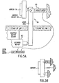
- the technique involves monitoring the bandwidth with wavemeter 104 shown in FIG. 5 and FIG. 6 . If the bandwidth is less than the desired bandwidth the wavelength control equipment is utilized to dither mirror 14 shown in FIG. 5 at frequent intervals to cause very slight shifts in the spectrum on a pulse to pulse basis so that the average integrated spectrum over a window of pulses simulates approximately a constant spectrum with bandwidth approximating the desired bandwidth.
- mirror 14 may be dithered about its nominal position to produce plus and minus shifts in the nominal wavelength of about 0.05 pm in order to maintain the same nominal wavelength with the effective increase by 0.1 pm.
- a change in the pivot position of mirror 14 of about 2 nm is required to produce a 0.05 pm shift in the wavelength. This change in mirror position is easily provided by the piezoelectric drivers referred to above and shown in FIG. 5A as item 80.
- each spot on the wafer is illuminated with a number of pulses usually in the range of about 30 to 150 pulses so that the dither rate should be sufficient so that each die spot receives about equal portions of pulses from both sides of the dither.
- the dither rate should be at least about 1 ⁇ 4 the pulse rate. So if the pulse rate is 2000 Hz the dither rate preferably would be at least 500 Hz This is no problem for the equipment and software referred to above.
- FIG. 2A shows the variation of focus with centerline wavelength for a modem 0.6 NA stepper type lithography using a line narrowed KrF light source having a FWHM bandwidth of about 0.35 pm.
- FIG. 2A also include a plot of the laser spectrum plotted as normalized intensity versus deviation from the centerline wavelength.
- the focus versus centerline wavelength slope for this system is -0.23 ⁇ m/pm.
- Applicants have shown that substantial improvements in lithographic imaging can be provided using a spectral engineering techniques developed by Applicants. Applicants refer to this technique as RELAX which is an acronym for Resolution Enhancement by Laser-Spectrum Adjusted Exposure.
- RELAX is an acronym for Resolution Enhancement by Laser-Spectrum Adjusted Exposure.
- the wafer is illuminated with two or more specific narrowband centerline wavelength during a single illumination period. This produces results which are improved over the dither technique referred to above.
- the results are similar to the FLEX technique discussed in the background section of this specification but constitutes a major improvement over FLEX since Applicants' technique involves only one positioning of the lithography equipment. Therefore, errors associated with adjustments of this equipment are avoided.
- the results of simulations performed by Applicants show proof of concept for use of a dual-mode illumination spectrum to improve resolution in photo resist film.
- Applicants simulated the process parameters for 200 nm isolated, semi-dense (1:2) and dense (1:1) contact hole patterns.
- a binary (chrome on glass) reticle pattern and conventional illumination e.g., a stepper system with a numerical aperture, NA of 0.7 and a 0.75 sigma
- the photo resist was modeled as UV6, 5200A casting thickness on AR2 bottom anti-reflective coating in order to quantify the obtained resolution enhancement of the imaged pattern.
- the double-mode spectrum used as the simulation input is shown in FIG. 2B .
- S( ⁇ ) represents the spectral density function of the nominal (0.45 pm/1.86 pm FWHM/E95%) spectrum
- S RELAX ( ⁇ ) S( ⁇ ) + S( ⁇ + 4 pm). Technologies for actual generation of such spectral properties are discussed in the following section.
- the longitudinal focus plane to centerline wavelength slope used for this model is -0.225 ⁇ m/pm which is shown in FIG. 2A .
- FIG. 2D presents plots of the resist feature widths of holes which have a target diameter of 200 nm as a function of depth of the holes.
- the figures are plotted for several doses ranging from 17 J/cm 2 to 26 J/cm 2 in the monochromatic example and from 25 J/cm 2 to 32 J/cm 2 in the RELAX example.
- This ordinant is feature width and the absissa is labeled focus but actually represents the depth of the feature in microns with zero taken as the focal plane of the centerline wavelength.
- An "ideal" graph would be a straight line at 200 nm over a depth of at least 1.0 ⁇ m (1.0 micron), with insignificant variation in width with exposure dose.
- the FIG. 1D plots reveal that the RELAX simulation produces a set of plots much closer to the "ideal" graph than either the conventional or monochromatic example.
- FIG. 2D is another set of graphs made from the same data as was used for the FIG. 2C plots.
- the exposure latitude i.e., the percent of the dose can vary without causing the critical dimension to vary more than 10% from a target value
- these three graphs show a great improvement in performance resulting from the use of the RELAX techniques.
- the dramatic improvement in the depth for which the critical dimension can be controlled to within 10% with the RELAX approach is apparent.
- the improvement in depth of focus is larger than fourfold at the 5% exposure latitude level compared to the monochromatic and conventional results for dense contacts.
- Some exposure latitude loss is observed by using the double-mode spectrum. This loss in exposure latitude is most pronounced near best focus (i.e., 0.0 depth of focus).
- the slight increase in the target dose from about 25 mJ/cm 2 to about 29 mJ/cm 2 ) for the RELAX case as compared to the conventional example should be noted.
- PZT driver 80 shown in FIG. 5A was programmed to control the wavelength of a KrF laser operating at 120 Hz to adjust each pulse by plus or minus steps of 4.0 pm.
- the integrated intensity values recorded on wavemeter photodiode array 180 shown in FIG. 6 are plotted in FIG. 2E . This plot shows sharp peaks at pixel 450 and 618 which correspond to a centerline wavelength shaft of 4.0 pm.
- the basic concept behind spectral engineering is to determine, using lithography simulation, the optimal spectral shape, which will provide the maximum improvement of a given parameter.
- lithography simulations are provided for two dual-mode illumination spectra and three three-mode illumination spectra shown in FIGS. 2G1 , 2G2 and 2G3 .
- the parameter, which is maximized is the depth of focus, for 150nm dense lines. From FIG. 2H1 , we see that the two dual-peak spectra (3pm and 4pm separation) are least sensitive to defocus and therefore have a maximum depth of focus.
- RELAX requires a very careful tradeoff design in order to maximize the benefits of a subset of imaging parameters at lowest cost to other parameters.
- the RELAX application will therefore be most successful in cases where a single parameter limits the overall process margin (process latitude). In that case, the limiting process parameter can be improved (relaxed) in order to improve to overall process margin for manufacturability.
- Optical proximity correction OPC-resolution enhancement technique using reticle feature corrections
- OPC-resolution enhancement technique using reticle feature corrections can be used in conjunction with RELAX for comprehensive lithography process engineering and maximum benefits.
- FIG. 2I shows the confluence of simulation and experiments (DOE) for either S( ⁇ ) spectrum optimization only or for a comprehensive lithography process optimization (variable lithography inputs) using RELAX.
- Wavelength and bandwidths have been measured on a pulse to pulse basis for every pulse, but typically the feedback control of wavelength has taken about 7 milli-seconds because prior art techniques for controlling center wavelength have taken several milli-seconds. Faster control is needed.
- a preferred embodiment of the present invention is an ArF excimer laser system capable of operation in the range of 4,000 Hz to 6,000 Hz with very fast measurement of laser beam parameters and very fast control of pulse energy and center wavelength. The beam parameter measurement and control for this laser is described below.
- the wavemeter used in the present embodiment is very similar to the one described in U.S. Patent No. 5,978,394 and some of the description below is extracted from that patent.
- FIG. 6 shows the layouts of a preferred wavemeter unit 104, an absolute wavelength reference calibration unit 190, and a wavemeter processor 197.
- the optical equipment in these units measure pulse energy, wavelength and bandwidth. These measurements are used with feedback circuits to maintain pulse energy and wavelength within desired limits.
- the equipment calibrates itself by reference to an atomic reference source on the command from the laser system control processor.
- the laser output beam intersects partially reflecting mirror 170, which passes about 95.5% of the beam energy as output beam 33 and reflects about 4.5% for pulse energy, wavelength and bandwidth measurement.
- energy detector 172 which comprises a very fast photo diode 69 which is able to measure the energy of individual pulses occurring at the rate of 4,000 pulses per second.
- the pulse energy for a typical ArF excimer laser is about 5 mJ, and the output of detector 69 is fed to a computer controller which uses a special algorithm to adjust the laser charging voltage to precisely control the pulse energy of future pulses based on stored pulse energy data in order to limit the variation of the energy of individual pulses and the integrated energy of bursts of pulses.
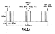
- Photo diode array 180 is an integrated circuit chip comprising 1024 separate photo diode integrated circuits and an associated sample and hold readout circuit as shown in FIG. 6A .
- the photo diodes are on a 25 micrometer pitch for a total length of 25.6 mm (about one inch). Each photo diode is 500 micrometers long.
- Photo diode arrays such as this are available from several sources.
- a preferred supplier is Hamamatsu.
- the PDA is designed for 2 x 10 6 pixel/sec operation but Applicants have found that it can be over-clocked to run much faster, i.e., up to 4 x 10 6 pixel/sec.
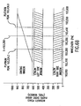
- the spatial position of the beam on the photo diode array is a coarse measure of the relative nominal wavelength of the output beam. For example, as shown in FIG. 6B , light in the wavelength range of about 193.350 pm would be focused on pixel 750 and its neighbors.
- the coarse wavelength optics in wavemeter module 120 produces a rectangular image of about 0.25 mm x 3 mm on the left side of photo diode array 180.
- the ten or eleven illuminated photo diodes will generate signals in proportion to the intensity of the illumination received (as indicated in FIG. 6C ) and the signals are read and digitized by a processor in wavemeter controller 197. Using this information and an interpolation algorithm controller 197 calculates the center position of the image.
- This position (measured in pixels) is converted into a coarse wavelength value using two calibration coefficients and assuming a linear relationship between position and wavelength.
- These calibration coefficients are determined by reference to an atomic wavelength reference source as described below.
- a diffuser preferably a diffraction diffuser as explained in a following section entitled "Improved Etalon"
- the beam exiting etalon 184 is focused by a 458.4 mm focal length lens in the etalon assembly and produces interference fringes on the middle and right side of linear photo diode array 180 after being reflected off two mirrors as shown in FIG. 6 .
- the spectrometer must measure wavelength and bandwidth substantially in real time. Because the laser repetition rate may be 4,000 Hz to 6,000 Hz, it is necessary to use algorithms which are accurate but not computationally intensive in order to achieve the desired performance with economical and compact processing electronics. Calculational algorithm therefore preferably should use integer as opposed to floating point math, and mathematical operations should preferably be computation efficient (no use of square root, sine, log, etc.).
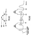
- FIG. 6D is a curve with 5 peaks as shown which represents a typical etalon fringe signal as measured by linear photo diode array 180.
- the central peak is drawn lower in height than the others. As different wavelengths of light enter the etalon, the central peak will rise and fall, sometimes going to zero. This aspect renders the central peak unsuitable for the wavelength measurements.
- the other peaks will move toward or away from the central peak in response to changes in wavelength, so the position of these peaks can be used to determine the wavelength, while their width measures the bandwidth of the laser.
- Two regions, each labeled data window, are shown in FIG. 6D . The data windows are located so that the fringe nearest the central peak is normally used for the analysis.
- the wavelength changes to move the fringe too close to the central peak which will cause distortion and resulting errors
- the first peak is outside the window, but the second closest peak will be inside the window, and the software causes the processor in control module 197 to use the second peak.
- the software will jump to an inner fringe within the data window.
- the data windows are also depicted on FIG. 6B .
- the hardware includes a microprocessor 400, Model MPC 823 supplied by Motorola with offices in Phoenix, Arizona; a programmable logic device 402, Model EP 6016QC240 supplied by Altera with offices in San Jose, California; an executive and data memory bank 404; a special very fast RAM 406 for temporary storage of photodiode array data in table form; a third 4X1024 pixel RAM memory bank 408 operating as a memory buffer; and an analog to digital converter 410.
- the basic technique is to use programmable logic device 402 to continuously produce a fringe data table from the PDA pixel data as the pixel data are produced.
- Logic device 402 also identifies which of the sets of fringe data represent fringe data of interest. Then when a calculation of center wavelength and bandwidth are needed, microprocessor merely picks up the data from the identified pixels of interest and calculates the needed values of center wavelength and bandwidth. This process reduces the calculation time for microprocessor by about a factor of about 10.
- microprocessor 400 secures the raw pixel data in the region of the two fringes from RAM memory bank 406 and calculates from that data the bandwidth and center wavelength. The calculation is as follows:
- Typical shape of the etalon fringes are shown in FIG. 6D .
- the fringe having a maximum at about pixel 180 and the fringe having a maximum at about pixel 450 will be identified to microprocessor 400.
- the pixel data surrounding these two maxima are analyzed by microprocessor 400 to define the shape and location of the fringe. This is done as follows:
- a half maximum value is determined by subtracting the fringe minimum from the fringe maximum dividing the difference by 2 and adding the result to the fringe minimum. For each rising edge and each falling edge of the two fringes the two pixels having values of closest above and closest below the half maximum value. Microprocessor then extrapolates between the two pixel values in each case to define the end points of D1 and D2 as shown in FIG. 6D with a precision of 1/32 pixel. From these values the inner diameter D1 and the outer diameter D2 of the circular fringe are determined.
- the fine wavelength calculation is made using the course wavelength measured value and the measured values of D1 and D2.
- the wavemeter's principal task is to calculate ⁇ from D. This requires knowing f, n, d and m. Since n and d are both intrinsic to the etalon we combine them into a single calibration constant named ND. We consider f to be another calibration constant named FD with units of pixels to match the units of D for a pure ratio. The integer order m varies depending on the wavelength and which fringe pair we choose. m is determined using the coarse fringe wavelength, which is sufficiently accurate for the purpose.
- FRAC Internally FRAC is represented as an unsigned 32 bit value with its radix point to the left of the most significant bit. FRAC is always just slightly less than one, so we get maximal precision there. FRAC ranges from [1 - 120E-6] to [1 - 25E-6] for D range of ⁇ 560 ⁇ 260 ⁇ pixels.
- the bandwidth of the laser is computed as ( ⁇ 2 - ⁇ 1 )/2.
- a fixed correction factor is applied to account for the intrinsic width of the etalon peak adding to the true laser bandwidth.
- ⁇ depends on both the etalon specifications and the true laser bandwidth. It typically lies in the range of 0.1-1 pm for the application described here.
- This embodiment utilizes an improved etalon.
- Conventional etalon mounting schemes typically employ an elastomer to mount the optical elements to the surrounding structure, to constrain the position of the elements but minimize forces applied to the elements.
- a compound commonly used for this is room-temperature vulcanizing silicone (RTV).
- RTV room-temperature vulcanizing silicone
- various organic vapors emitted from these elastomers can deposit onto the optical surfaces, degrading their performance.
- a preferred embodiment includes an improved etalon assembly shown at 184 in FIGS. 6 and 6E .
- the fused silica etalon 79 shown in FIG. 6G itself is comprised of a top plate 80 having a flange 81 and a lower plate 82, both plates being comprised of premium grade fused silica.
- the etalon is designed to produce fringes having free spectral range of 20.00 pm at 193.35 nm when surrounded by gas with an index of refraction of 1.0003 and a finesse equal to or greater than 25.
- Three fused silica spacers 83 with ultra low thermal expansion separate the plates and are 934 ⁇ m ⁇ 1 ⁇ m thick.
- the reflectance of the inside surfaces of the etalon are each about 88 percent and the outside surfaces are anti-reflection coated.
- the transmission of the etalon is about 50 percent.
- the etalon 79 is held in place in aluminum housing 84 only by gravity and three low force springs 86 pressing the flange against three pads not shown but positioned on 120 degree centers under the bottom edge of flange 81 at the radial location indicated by leader 85.
- a clearance of only 0.004 inch along the top edge of flange 81 at 87 assures that the etalon will remain approximately in its proper position. This close tolerance fit also ensures that if any shock or impulse is transferred to the etalon system through the mounting, the relative velocities between the optical components and the housing contact points will be kept to a minimum.
- Other optical components of etalon assembly 184 include diffuser 88, window 89 and focusing lens 90 having a focal length of 458.4 mm.
- the diffuser 88 may be a standard prior art diffuser commonly used up-stream of an etalon to produce a great variety of incident angles needed for the proper operation of the etalon.
- a problem with prior art diffusers is that about 90 percent of the light passing through the diffuser is not at a useful angle and consequently is not focused on the photo diode array. This wasted light, however, adds to the heating of the optical system and can contribute to degradation of optical surfaces.
- a diffractive lens array is used as the diffuser 88. With this type of diffuser, a pattern is produced in the diffractive lens array which scatters the light thoroughly but only within an angle of about 5 degrees.
- the incident light can be greatly reduced which greatly increases optical component life. Applicants estimate that the incident light can be reduced to less than 5% or 10% of prior art values with equivalent light on the photo diode array.
- FIG. 6H shows features of a preferred embodiment providing even further reduction of light intensity passing through the etalon.
- This embodiment is similar to the embodiment discussed above.
- the sample beam from mirror 182 (approximately 15mm x 3mm) passes upward through condensing lens 400 and is then re-collimated by lens 402.
- the beam now colliminated and reduced in dimension to about 5mm x 1mm passes through etalon housing window 404 and then passes through a diffractive diffusing element 406 which in this case (for an ArF laser) is a diffractive diffusing element provided by Mems Optical, Inc. with offices in Huntsville, Alabama.
- the element is part number D023-193 which converts substantially all 193nm light in any incoming collimated beam of any cross sectional configuration into a beam expanding in a first direction at 2° and in a second direction perpendicular to the first direction at 4°.
- Lens 410 then "focuses" the expanding beam onto a rectangular pattern covering photodiode array 180 shown in FIG. 6 .
- the active area of the photo diode array is about 0.5mm wide and 25.6 mm long and the spot pattern formed by lens 410 is about 15mm x 30mm.
- Diffractive diffusing element thoroughly mixes the spatial components of the beam but maintains substantially all of the beam energy within the 2° and 4° limits so that the light passing through the etalon can be substantially reduced and efficiently utilized.
- lens 400 has a focal length of about 50mm.
- the lens is Melles Griot Corporation part number OILQP001.
- Collimating lens 402 has a focal length of -20mm (EVI Laser Corporation part number PLCC-10.0-10.3-UV).
- the diffractive diffusing element 406 is Mems Optical Corporation part number DO23-248.
- the spacing between the two lenses can be properly positioned with spacer 416. Applicants estimate that the energy of the beam passing through the etalon with the laser operating at 2000Hz is about 10mw and is not sufficient to cause significant thermal problems in the etalon.
- the beam could be allowed to come to a focus between lenses 400 and 402.
- Appropriate lenses would in this case be chosen using well known optical techniques.
- the pulse energy of subsequent pulses are controlled to maintain desired pulse energies and also desired total integrated dose of a specified number of pulses all as described in U.S. Patent No. 6,005,879 , Pulse Energy Control for Excimer Laser.
- Wavelength of the laser may be controlled in a feedback arrangement using measured values of wavelengths and techniques known in the prior art such as those techniques described in U.S. Patent No. 5,978,394 , Wavelength System for an Excimer Laser.
- Applicants have recently developed techniques for wavelength tuning which utilize a piezoelectric driver to provide extremely fast movement of tuning mirror. Some of these techniques are described in United States Patent Application Serial No. 608,543 , Bandwidth Control Technique for a Laser, filed June 30, 2000.
- FIGS. 8A and 8B are extracted from that application and show the principal elements of this technique.
- a piezoelectric stack is used for very fast mirror adjustment and larger slower adjustments are provided by a prior art stepper motor operating a lever arm. The piezoelectric stack adjusts the position of the fulcrum of the lever arm.
- FIG. 8 is a block diagram showing features of the laser system which are important for controlling the wavelength and pulse energy of the output laser beam. Shown are a line narrowing module 15K which contains a three prism beam expander, a tuning mirror 14 and a grating Wavemeter 104 monitors the output beam wavelength and provides a feedback signal to LNP processor 106 which controls the position of tuning mirror 14 by operation of a stepper motor and a PZT stack as described below. Operational wavelengths can be selected by laser controller 102. Pulse energy is also measured in wavemeter 104 which provides a signal used by controller 102 to control pulse energy in a feedback arrangement as described above.
- FIG. 8A is a block diagram showing PZT stack 80, stepper motor 82, mirror 14 and mirror mount 86.
- FIG. 8B1 is a drawing showing detail features of a preferred embodiment of the present invention.
- Large changes in the position of mirror 14 are produced by stepper motor through a 26.5 to 1 lever arm 84.
- a diamond pad 41 at the end of piezoelectric drive 80 is provided to contact spherical tooling ball at the fulcrum of lever arm 84.
- the contact between the top of lever arm 84 and mirror mount 86 is provided with a cylindrical dowel pin on the lever arm and four spherical ball bearings mounted (only two of which are shown) on the mirror mount as shown at 85.
- Piezoelectric drive 80 is mounted on the LNP frame with piezoelectric mount 80A and the stepper motor is mounted to the frame with stepper motor mount 82A.
- Mirror 14 is mounted in mirror mount 86 with a three point mount using three aluminum spheres, only one of which are shown in FIG. 8B1 .
- Three springs 14A apply the compressive force to hold the mirror against the spheres.
- FIG. 8B2 is a preferred embodiment slightly different from the one shown in FIG. 8B1 .
- This embodiment includes a bellows 87 to isolate the piezoelectric drive from the environment inside the LNP. This isolation prevents UV damage to the piezoelectric element and avoid possible contamination caused by out-gassing from the piezoelectric materials.
- FIG. 8C shows actual test data from a laser fitted with the FIG. 8B2 embodiment.
- the graph is a plot of the deviation from target wavelength of the average of 30 pulse windows. The deviation is reduced from about 0.05 pm to about 0.005 pm.
- This embodiment is a major speed up as compared to the stepper motor drive system described above but not quite fast enough for pulse-to-pulse adjustment.
- Earlier methods of mirror positioning required about 7 ms to move mirror 14, making pulse-to-pulse wavelength correction at 2000 Hz out of the question.
- a lever arm pivoted about a pivot axis to produce a 1 to 26.5 reduction in the mirror movement compared to the stepper position movement.
- the prior art stepper has a total travel of 1 ⁇ 2 inch (12.7 mm) and 6000 steps so that each step is a distance of about 2 microns. With the 1-26.5 reduction, one step moves the mirror about 75 nm which typically changes the wavelength of the laser wavelength about 0.1 pm.
- a piezo stack 80 has been added at the pivot position of the lever arm.
- a preferred piezo stack is Model P-840.10 supplied by Physik Instrumente GmbH with offices in Waldbronn, Germany.
- This stack will produce linear adjustment of about 3.0 microns with a drive voltage change of 20 volts. This range is equivalent to about ⁇ 20 steps of the stepper motor.
- the stack responds to a control signal within less than 1 microsecond and the system can easily respond to updated signals at a frequency of 4000 Hz.
- the control for each pulse at 4000 Hz pulse rate is based not on the previous pulse but the pulse prior to the previous pulse to allow plenty of time for the wavelength calculation.
- this embodiment provides a factor of 7 improvement over the prior art design with a 7 millisecond latency. Therefore, much faster feedback control can be provided.
- FIG. 8D One preferred feedback control algorithm is described in FIG. 8D . In this algorithm the wavelength is measured for each pulse and an average wavelength for the last four and last two pulses is calculated. If either of the averages deviate from the target wavelength by less than 0.02 pm, no adjustment is made.
- piezoelectric stack 80 If both deviate more than 0.02 pm from the target, an adjustment is made to the mirror assembly by piezoelectric stack 80 to provide a wavelength correction. Which of the two averages is used is determined by how much time had elapsed since the last adjustment.
- the piezoelectric stack is maintained within its control range by stepping the stepper motor as the stack approaches 30 and 70 percent of its range (or to provide more available range, 45 and 55 percent could be used instead of the 30 and 70 percent range values). Since the stepper motor requires about 7 ms to complete a step, the algorithm may make several piezo adjustments during a stepper motor step.
Landscapes
- Physics & Mathematics (AREA)
- Electromagnetism (AREA)
- Engineering & Computer Science (AREA)
- Plasma & Fusion (AREA)
- Optics & Photonics (AREA)
- General Physics & Mathematics (AREA)
- Public Health (AREA)
- Epidemiology (AREA)
- Health & Medical Sciences (AREA)
- Atmospheric Sciences (AREA)
- Life Sciences & Earth Sciences (AREA)
- Environmental & Geological Engineering (AREA)
- Lasers (AREA)
- Exposure And Positioning Against Photoresist Photosensitive Materials (AREA)
Applications Claiming Priority (5)
| Application Number | Priority Date | Filing Date | Title |
|---|---|---|---|
| US09/854,097 US6757316B2 (en) | 1999-12-27 | 2001-05-11 | Four KHz gas discharge laser |
| US854097 | 2001-05-11 | ||
| US918773 | 2001-07-27 | ||
| US09/918,773 US6671294B2 (en) | 1997-07-22 | 2001-07-27 | Laser spectral engineering for lithographic process |
| PCT/US2002/012396 WO2002093700A1 (en) | 2001-05-11 | 2002-04-19 | Laser spectral engineering for lithographic process |
Publications (3)
| Publication Number | Publication Date |
|---|---|
| EP1386376A1 EP1386376A1 (en) | 2004-02-04 |
| EP1386376A4 EP1386376A4 (en) | 2006-06-28 |
| EP1386376B1 true EP1386376B1 (en) | 2010-09-01 |
Family
ID=27127208
Family Applications (1)
| Application Number | Title | Priority Date | Filing Date |
|---|---|---|---|
| EP02731433A Expired - Lifetime EP1386376B1 (en) | 2001-05-11 | 2002-04-19 | Laser spectral engineering for lithographic process |
Country Status (6)
| Country | Link |
|---|---|
| US (2) | US6671294B2 (enExample) |
| EP (1) | EP1386376B1 (enExample) |
| JP (1) | JP4437006B2 (enExample) |
| DE (1) | DE60237515D1 (enExample) |
| TW (1) | TW541607B (enExample) |
| WO (1) | WO2002093700A1 (enExample) |
Families Citing this family (97)
| Publication number | Priority date | Publication date | Assignee | Title |
|---|---|---|---|---|
| US6853653B2 (en) | 1997-07-22 | 2005-02-08 | Cymer, Inc. | Laser spectral engineering for lithographic process |
| US6567450B2 (en) | 1999-12-10 | 2003-05-20 | Cymer, Inc. | Very narrow band, two chamber, high rep rate gas discharge laser system |
| US20020127497A1 (en) * | 1998-09-10 | 2002-09-12 | Brown Daniel J. W. | Large diffraction grating for gas discharge laser |
| US6625191B2 (en) * | 1999-12-10 | 2003-09-23 | Cymer, Inc. | Very narrow band, two chamber, high rep rate gas discharge laser system |
| US6914919B2 (en) * | 2000-06-19 | 2005-07-05 | Cymer, Inc. | Six to ten KHz, or greater gas discharge laser system |
| US6912052B2 (en) | 2000-11-17 | 2005-06-28 | Cymer, Inc. | Gas discharge MOPA laser spectral analysis module |
| US6750972B2 (en) * | 2000-11-17 | 2004-06-15 | Cymer, Inc. | Gas discharge ultraviolet wavemeter with enhanced illumination |
| US6553559B2 (en) * | 2001-01-05 | 2003-04-22 | International Business Machines Corporation | Method to determine optical proximity correction and assist feature rules which account for variations in mask dimensions |
| US6713770B2 (en) * | 2001-01-29 | 2004-03-30 | Cymer, Inc. | High resolution spectral measurement device |
| US7039086B2 (en) * | 2001-04-09 | 2006-05-02 | Cymer, Inc. | Control system for a two chamber gas discharge laser |
| US6690704B2 (en) | 2001-04-09 | 2004-02-10 | Cymer, Inc. | Control system for a two chamber gas discharge laser |
| US7079564B2 (en) * | 2001-04-09 | 2006-07-18 | Cymer, Inc. | Control system for a two chamber gas discharge laser |
| US7009140B2 (en) * | 2001-04-18 | 2006-03-07 | Cymer, Inc. | Laser thin film poly-silicon annealing optical system |
| US7061959B2 (en) * | 2001-04-18 | 2006-06-13 | Tcz Gmbh | Laser thin film poly-silicon annealing system |
| US7439530B2 (en) * | 2005-06-29 | 2008-10-21 | Cymer, Inc. | LPP EUV light source drive laser system |
| US7465946B2 (en) | 2004-03-10 | 2008-12-16 | Cymer, Inc. | Alternative fuels for EUV light source |
| US7378673B2 (en) * | 2005-02-25 | 2008-05-27 | Cymer, Inc. | Source material dispenser for EUV light source |
| US20050259709A1 (en) * | 2002-05-07 | 2005-11-24 | Cymer, Inc. | Systems and methods for implementing an interaction between a laser shaped as a line beam and a film deposited on a substrate |
| US7598509B2 (en) | 2004-11-01 | 2009-10-06 | Cymer, Inc. | Laser produced plasma EUV light source |
| US7372056B2 (en) * | 2005-06-29 | 2008-05-13 | Cymer, Inc. | LPP EUV plasma source material target delivery system |
| US7088758B2 (en) | 2001-07-27 | 2006-08-08 | Cymer, Inc. | Relax gas discharge laser lithography light source |
| US7154928B2 (en) * | 2004-06-23 | 2006-12-26 | Cymer Inc. | Laser output beam wavefront splitter for bandwidth spectrum control |
| US6963595B2 (en) | 2001-08-29 | 2005-11-08 | Cymer, Inc. | Automatic gas control system for a gas discharge laser |
| US7830934B2 (en) * | 2001-08-29 | 2010-11-09 | Cymer, Inc. | Multi-chamber gas discharge laser bandwidth control through discharge timing |
| US20050100072A1 (en) * | 2001-11-14 | 2005-05-12 | Rao Rajasekhar M. | High power laser output beam energy density reduction |
| US7741639B2 (en) * | 2003-01-31 | 2010-06-22 | Cymer, Inc. | Multi-chambered excimer or molecular fluorine gas discharge laser fluorine injection control |
| US7218443B2 (en) * | 2003-02-25 | 2007-05-15 | Toptica Photonics Ag | Generation of tunable light pulses |
| US20040190577A1 (en) * | 2003-02-27 | 2004-09-30 | Hans-Stephan Albrecht | Fast linear motor for wavelength variation for lithography lasers |
| US7217941B2 (en) * | 2003-04-08 | 2007-05-15 | Cymer, Inc. | Systems and methods for deflecting plasma-generated ions to prevent the ions from reaching an internal component of an EUV light source |
| US7277188B2 (en) * | 2003-04-29 | 2007-10-02 | Cymer, Inc. | Systems and methods for implementing an interaction between a laser shaped as a line beam and a film deposited on a substrate |
| EP1517183A1 (en) | 2003-08-29 | 2005-03-23 | ASML Netherlands B.V. | Lithographic apparatus, device manufacturing method, and device manufactured thereby |
| EP1510869A3 (en) * | 2003-08-29 | 2009-07-29 | ASML Netherlands B.V. | Lithographic apparatus, device manufacturing method, and device manufactured thereby |
| US6894785B2 (en) * | 2003-09-30 | 2005-05-17 | Cymer, Inc. | Gas discharge MOPA laser spectral analysis module |
| US6873418B1 (en) | 2003-09-30 | 2005-03-29 | Cymer, Inc. | Optical mountings for gas discharge MOPA laser spectral analysis module |
| US6829040B1 (en) | 2003-11-07 | 2004-12-07 | Advanced Micro Devices, Inc. | Lithography contrast enhancement technique by varying focus with wavelength modulation |
| WO2005081295A1 (ja) * | 2004-02-20 | 2005-09-01 | Nikon Corporation | 露光方法、露光装置及び露光システム並びにデバイス製造方法 |
| US7196342B2 (en) * | 2004-03-10 | 2007-03-27 | Cymer, Inc. | Systems and methods for reducing the influence of plasma-generated debris on the internal components of an EUV light source |
| US20050243876A1 (en) * | 2004-04-29 | 2005-11-03 | Academia Sinica | Narrow bandwidth high repetition rate optical parametric oscillator |
| US20050286599A1 (en) * | 2004-06-29 | 2005-12-29 | Rafac Robert J | Method and apparatus for gas discharge laser output light coherency reduction |
| US7352791B2 (en) * | 2004-07-27 | 2008-04-01 | Corning Incorporated | Optical systems including wavefront correcting optical surfaces |
| US7355191B2 (en) * | 2004-11-01 | 2008-04-08 | Cymer, Inc. | Systems and methods for cleaning a chamber window of an EUV light source |
| US7643522B2 (en) * | 2004-11-30 | 2010-01-05 | Cymer, Inc. | Method and apparatus for gas discharge laser bandwidth and center wavelength control |
| US7366219B2 (en) * | 2004-11-30 | 2008-04-29 | Cymer, Inc. | Line narrowing module |
| US20060114956A1 (en) * | 2004-11-30 | 2006-06-01 | Sandstrom Richard L | High power high pulse repetition rate gas discharge laser system bandwidth management |
| JP4580338B2 (ja) * | 2004-12-23 | 2010-11-10 | エーエスエムエル ネザーランズ ビー.ブイ. | リソグラフィ装置、エキシマ・レーザ、およびデバイス製造方法 |
| US7534552B2 (en) * | 2004-12-23 | 2009-05-19 | Asml Netherlands B.V. | Lithographic apparatus and device manufacturing method |
| US20060139607A1 (en) * | 2004-12-23 | 2006-06-29 | Asml Netherlands B.V. | Lithographic apparatus and device manufacturing method |
| US7256870B2 (en) * | 2005-02-01 | 2007-08-14 | Asml Netherlands B.V. | Method and apparatus for controlling iso-dense bias in lithography |
| US7482609B2 (en) * | 2005-02-28 | 2009-01-27 | Cymer, Inc. | LPP EUV light source drive laser system |
| US7525638B2 (en) * | 2005-03-23 | 2009-04-28 | Asml Netherlands B.V. | Lithographic apparatus and device manufacturing method |
| US20060222034A1 (en) * | 2005-03-31 | 2006-10-05 | Cymer, Inc. | 6 Khz and above gas discharge laser system |
| US7286207B2 (en) * | 2005-04-28 | 2007-10-23 | Infineon Technologies, Ag | Exposing a semiconductor wafer using two different spectral wavelengths and adjusting for chromatic aberration |
| US7443484B2 (en) * | 2005-05-13 | 2008-10-28 | Infineon Technologies Ag | Method for exposing a semiconductor wafer by applying periodic movement to a component |
| US7180083B2 (en) * | 2005-06-27 | 2007-02-20 | Cymer, Inc. | EUV light source collector erosion mitigation |
| US7365349B2 (en) * | 2005-06-27 | 2008-04-29 | Cymer, Inc. | EUV light source collector lifetime improvements |
| US7317536B2 (en) | 2005-06-27 | 2008-01-08 | Cymer, Inc. | Spectral bandwidth metrology for high repetition rate gas discharge lasers |
| US7141806B1 (en) | 2005-06-27 | 2006-11-28 | Cymer, Inc. | EUV light source collector erosion mitigation |
| US7653095B2 (en) * | 2005-06-30 | 2010-01-26 | Cymer, Inc. | Active bandwidth control for a laser |
| US8379687B2 (en) | 2005-06-30 | 2013-02-19 | Cymer, Inc. | Gas discharge laser line narrowing module |
| US7394083B2 (en) | 2005-07-08 | 2008-07-01 | Cymer, Inc. | Systems and methods for EUV light source metrology |
| US7679029B2 (en) * | 2005-10-28 | 2010-03-16 | Cymer, Inc. | Systems and methods to shape laser light as a line beam for interaction with a substrate having surface variations |
| US7317179B2 (en) * | 2005-10-28 | 2008-01-08 | Cymer, Inc. | Systems and methods to shape laser light as a homogeneous line beam for interaction with a film deposited on a substrate |
| US7321607B2 (en) * | 2005-11-01 | 2008-01-22 | Cymer, Inc. | External optics and chamber support system |
| US7453077B2 (en) * | 2005-11-05 | 2008-11-18 | Cymer, Inc. | EUV light source |
| KR100702845B1 (ko) * | 2006-01-20 | 2007-04-03 | 삼성전자주식회사 | 엑시머 레이저 및 그의 협대역 모듈 |
| US7822084B2 (en) * | 2006-02-17 | 2010-10-26 | Cymer, Inc. | Method and apparatus for stabilizing and tuning the bandwidth of laser light |
| US7852889B2 (en) | 2006-02-17 | 2010-12-14 | Cymer, Inc. | Active spectral control of DUV light source |
| US8518030B2 (en) * | 2006-03-10 | 2013-08-27 | Amo Manufacturing Usa, Llc | Output energy control for lasers |
| JP2007250947A (ja) * | 2006-03-17 | 2007-09-27 | Canon Inc | 露光装置および像面検出方法 |
| JP2008140956A (ja) * | 2006-12-01 | 2008-06-19 | Canon Inc | 露光装置 |
| US7720120B2 (en) * | 2008-10-21 | 2010-05-18 | Cymer, Inc. | Method and apparatus for laser control in a two chamber gas discharge laser |
| US7751453B2 (en) * | 2008-10-21 | 2010-07-06 | Cymer, Inc. | Method and apparatus for laser control in a two chamber gas discharge laser |
| US7756171B2 (en) * | 2008-10-21 | 2010-07-13 | Cymer, Inc. | Method and apparatus for laser control in a two chamber gas discharge laser |
| US8520186B2 (en) * | 2009-08-25 | 2013-08-27 | Cymer, Llc | Active spectral control of optical source |
| NL2006073A (en) * | 2010-02-12 | 2011-08-15 | Asml Netherlands Bv | Lithographic apparatus and method. |
| JP5410396B2 (ja) | 2010-03-23 | 2014-02-05 | ギガフォトン株式会社 | レーザ装置 |
| US8837536B2 (en) | 2010-04-07 | 2014-09-16 | Cymer, Llc | Method and apparatus for controlling light bandwidth |
| CN103309166B (zh) * | 2012-03-09 | 2016-03-30 | 上海微电子装备有限公司 | 可动镜片调整装置及应用其的可调式光学系统 |
| US9207119B2 (en) | 2012-04-27 | 2015-12-08 | Cymer, Llc | Active spectral control during spectrum synthesis |
| US9715180B2 (en) | 2013-06-11 | 2017-07-25 | Cymer, Llc | Wafer-based light source parameter control |
| US10416566B2 (en) | 2015-12-14 | 2019-09-17 | Asml Netherlands B.V. | Optimization of source and bandwidth for new and existing patterning devices |
| US10416471B2 (en) | 2016-10-17 | 2019-09-17 | Cymer, Llc | Spectral feature control apparatus |
| US9997888B2 (en) | 2016-10-17 | 2018-06-12 | Cymer, Llc | Control of a spectral feature of a pulsed light beam |
| US9835959B1 (en) | 2016-10-17 | 2017-12-05 | Cymer, Llc | Controlling for wafer stage vibration |
| US9989866B2 (en) | 2016-10-17 | 2018-06-05 | Cymer, Llc | Wafer-based light source parameter control |
| US10288483B2 (en) * | 2017-04-09 | 2019-05-14 | Cymer, Llc | Recovering spectral shape from spatial output |
| KR102428750B1 (ko) * | 2017-10-19 | 2022-08-02 | 사이머 엘엘씨 | 단일의 리소그래피 노광 패스로 복수의 에어리얼 이미지를 형성하는 방법 |
| CN111819741A (zh) | 2018-03-12 | 2020-10-23 | Asml荷兰有限公司 | 控制系统和方法 |
| KR102462465B1 (ko) * | 2018-03-30 | 2022-11-02 | 사이머 엘엘씨 | 펄스형 광 빔의 스펙트럼 특성 선택 및 펄스 타이밍 제어 기술 |
| CN112889004B (zh) * | 2018-10-19 | 2024-06-28 | Asml荷兰有限公司 | 通过源和掩模优化创建理想源光谱的方法 |
| CN111385020B (zh) * | 2018-12-29 | 2022-04-29 | 海思光电子有限公司 | 一种波长测量装置 |
| TWI749546B (zh) * | 2019-05-14 | 2021-12-11 | 美商希瑪有限責任公司 | 用於調變光源波長的裝置及方法 |
| JP7382424B2 (ja) | 2019-05-22 | 2023-11-16 | サイマー リミテッド ライアビリティ カンパニー | 複数の深紫外光発振器のための制御システム |
| JP7358610B2 (ja) | 2019-07-23 | 2023-10-10 | サイマー リミテッド ライアビリティ カンパニー | 繰り返し率のずれによって誘発される波長誤差を補償する方法 |
| CN114787715A (zh) * | 2019-12-02 | 2022-07-22 | 西默有限公司 | 用于增强成像到衬底上的图案的目标特征的方法和系统 |
| US12276897B2 (en) | 2022-09-06 | 2025-04-15 | Orbotech Ltd. | Dynamic correction for an acousto-optic deflector |
| CN115473119B (zh) * | 2022-10-10 | 2024-06-25 | 湖南五凌电力科技有限公司 | 一种可调谐半导体激光器调制电路 |
Family Cites Families (52)
| Publication number | Priority date | Publication date | Assignee | Title |
|---|---|---|---|---|
| US4223279A (en) | 1977-07-18 | 1980-09-16 | Mathematical Sciences Northwest, Inc. | Pulsed electric discharge laser utilizing water dielectric blumlein transmission line |
| US4455658A (en) | 1982-04-20 | 1984-06-19 | Sutter Jr Leroy V | Coupling circuit for use with a transversely excited gas laser |
| US4883352A (en) * | 1984-06-21 | 1989-11-28 | American Telephone And Telegraph Company | Deep-uv lithography |
| US4599730A (en) * | 1984-10-01 | 1986-07-08 | The United States Of America As Represented By The Secretary Of The Navy | Visible and ultraviolet lasers based on excimer transitions in the homonuclear halogens |
| US4937619A (en) * | 1986-08-08 | 1990-06-26 | Hitachi, Ltd. | Projection aligner and exposure method |
| US4697270A (en) | 1986-08-27 | 1987-09-29 | The United States Of America As Represented By The United States Department Of Energy | Copper vapor laser acoustic thermometry system |
| US4940331A (en) | 1986-09-24 | 1990-07-10 | The United States Of America As Represented By The United States Department Of Energy | Heterodyne laser instantaneous frequency measurement system |
| US4798467A (en) | 1986-09-24 | 1989-01-17 | The United States Department Of Energy | Heterodyne laser instantaneous frequency measurement system |
| US5315611A (en) | 1986-09-25 | 1994-05-24 | The United States Of America As Represented By The United States Department Of Energy | High average power magnetic modulator for metal vapor lasers |
| US5189678A (en) | 1986-09-29 | 1993-02-23 | The United States Of America As Represented By The United States Department Of Energy | Coupling apparatus for a metal vapor laser |
| US4817101A (en) | 1986-09-26 | 1989-03-28 | The United States Of America As Represented By The United States Department Of Energy | Heterodyne laser spectroscopy system |
| WO1989000779A1 (fr) * | 1987-07-17 | 1989-01-26 | Kabushiki Kaisha Komatsu Seisakusho | Dispositif de regulation de la longueur d'onde d'un rayon laser |
| US4823354A (en) * | 1987-12-15 | 1989-04-18 | Lumonics Inc. | Excimer lasers |
| US4959840A (en) | 1988-01-15 | 1990-09-25 | Cymer Laser Technologies | Compact excimer laser including an electrode mounted in insulating relationship to wall of the laser |
| US5023884A (en) | 1988-01-15 | 1991-06-11 | Cymer Laser Technologies | Compact excimer laser |
| US5025446A (en) | 1988-04-01 | 1991-06-18 | Laserscope | Intra-cavity beam relay for optical harmonic generation |
| US4881231A (en) * | 1988-11-28 | 1989-11-14 | Kantilal Jain | Frequency-stabilized line-narrowed excimer laser source system for high resolution lithography |
| IL91240A (en) | 1989-08-07 | 1994-07-31 | Quick Tech Ltd | Pulsed laser apparatus and systems and techniques for its operation |
| US5025445A (en) | 1989-11-22 | 1991-06-18 | Cymer Laser Technologies | System for, and method of, regulating the wavelength of a light beam |
| US5095492A (en) | 1990-07-17 | 1992-03-10 | Cymer Laser Technologies | Spectral narrowing technique |
| US5471965A (en) | 1990-12-24 | 1995-12-05 | Kapich; Davorin D. | Very high speed radial inflow hydraulic turbine |
| US5691989A (en) | 1991-07-26 | 1997-11-25 | Accuwave Corporation | Wavelength stabilized laser sources using feedback from volume holograms |
| US5347392A (en) * | 1992-02-26 | 1994-09-13 | The United States Of America As Represented By The Administrator Of The National Aeronautics And Space Administration | Electric-optic resonant phase modulator |
| US5371587A (en) | 1992-05-06 | 1994-12-06 | The Boeing Company | Chirped synthetic wavelength laser radar |
| JP3155837B2 (ja) | 1992-09-14 | 2001-04-16 | 株式会社東芝 | 光伝送装置 |
| US5303002A (en) * | 1993-03-31 | 1994-04-12 | Intel Corporation | Method and apparatus for enhancing the focus latitude in lithography |
| US5420877A (en) | 1993-07-16 | 1995-05-30 | Cymer Laser Technologies | Temperature compensation method and apparatus for wave meters and tunable lasers controlled thereby |
| US5440578B1 (en) * | 1993-07-16 | 2000-10-24 | Cymer Inc | Gas replenishment method ad apparatus for excimer lasers |
| US5448580A (en) | 1994-07-05 | 1995-09-05 | The United States Of America As Represented By The United States Department Of Energy | Air and water cooled modulator |
| JPH08172233A (ja) | 1994-12-15 | 1996-07-02 | Anritsu Corp | 可変波長光源装置 |
| JP3175515B2 (ja) * | 1994-12-26 | 2001-06-11 | キヤノン株式会社 | 露光装置及びそれを用いたデバイスの製造方法 |
| US5706301A (en) | 1995-08-16 | 1998-01-06 | Telefonaktiebolaget L M Ericsson | Laser wavelength control system |
| US5991324A (en) | 1998-03-11 | 1999-11-23 | Cymer, Inc. | Reliable. modular, production quality narrow-band KRF excimer laser |
| US6128323A (en) | 1997-04-23 | 2000-10-03 | Cymer, Inc. | Reliable modular production quality narrow-band high REP rate excimer laser |
| US5982800A (en) | 1997-04-23 | 1999-11-09 | Cymer, Inc. | Narrow band excimer laser |
| US5856991A (en) | 1997-06-04 | 1999-01-05 | Cymer, Inc. | Very narrow band laser |
| US6018537A (en) | 1997-07-18 | 2000-01-25 | Cymer, Inc. | Reliable, modular, production quality narrow-band high rep rate F2 laser |
| US5852621A (en) | 1997-07-21 | 1998-12-22 | Cymer, Inc. | Pulse laser with pulse energy trimmer |
| US5870420A (en) | 1997-08-18 | 1999-02-09 | Cymer, Inc. | Cross-flow blower with braces |
| WO1999012235A1 (en) | 1997-09-05 | 1999-03-11 | Micron Optics, Inc. | Tunable fiber fabry-perot surface-emitting lasers |
| US5953360A (en) | 1997-10-24 | 1999-09-14 | Synrad, Inc. | All metal electrode sealed gas laser |
| US5978405A (en) | 1998-03-06 | 1999-11-02 | Cymer, Inc. | Laser chamber with minimized acoustic and shock wave disturbances |
| US6477193B2 (en) | 1998-07-18 | 2002-11-05 | Cymer, Inc. | Extreme repetition rate gas discharge laser with improved blower motor |
| US6208675B1 (en) | 1998-08-27 | 2001-03-27 | Cymer, Inc. | Blower assembly for a pulsed laser system incorporating ceramic bearings |
| US6067311A (en) | 1998-09-04 | 2000-05-23 | Cymer, Inc. | Excimer laser with pulse multiplier |
| US6208674B1 (en) | 1998-09-18 | 2001-03-27 | Cymer, Inc. | Laser chamber with fully integrated electrode feedthrough main insulator |
| EP1147582A4 (en) * | 1998-12-15 | 2006-03-15 | Cymer Inc | ARF LASER WITH LOW PULSE ENERGY AND HIGH REPLAY RATE |
| US6154470A (en) * | 1999-02-10 | 2000-11-28 | Lamba Physik Gmbh | Molecular fluorine (F2) laser with narrow spectral linewidth |
| US6219368B1 (en) | 1999-02-12 | 2001-04-17 | Lambda Physik Gmbh | Beam delivery system for molecular fluorine (F2) laser |
| US6104735A (en) | 1999-04-13 | 2000-08-15 | Cymer, Inc. | Gas discharge laser with magnetic bearings and magnetic reluctance centering for fan drive assembly |
| US6164116A (en) | 1999-05-06 | 2000-12-26 | Cymer, Inc. | Gas module valve automated test fixture |
| US6483628B1 (en) * | 1999-09-20 | 2002-11-19 | The Board Of Trustees Of The Leland Stanford Junior University | Polarization and wavelength stable superfluorescent sources using Faraday rotator mirrors |
-
2001
- 2001-07-27 US US09/918,773 patent/US6671294B2/en not_active Expired - Lifetime
-
2002
- 2002-04-19 WO PCT/US2002/012396 patent/WO2002093700A1/en not_active Ceased
- 2002-04-19 DE DE60237515T patent/DE60237515D1/de not_active Expired - Lifetime
- 2002-04-19 JP JP2002590463A patent/JP4437006B2/ja not_active Expired - Lifetime
- 2002-04-19 EP EP02731433A patent/EP1386376B1/en not_active Expired - Lifetime
- 2002-04-26 TW TW091108726A patent/TW541607B/zh not_active IP Right Cessation
-
2003
- 2003-11-03 US US10/701,280 patent/US7139301B2/en not_active Expired - Fee Related
Also Published As
| Publication number | Publication date |
|---|---|
| WO2002093700A1 (en) | 2002-11-21 |
| US6671294B2 (en) | 2003-12-30 |
| EP1386376A4 (en) | 2006-06-28 |
| EP1386376A1 (en) | 2004-02-04 |
| US7139301B2 (en) | 2006-11-21 |
| JP4437006B2 (ja) | 2010-03-24 |
| TW541607B (en) | 2003-07-11 |
| JP2005501399A (ja) | 2005-01-13 |
| US20020048288A1 (en) | 2002-04-25 |
| US20040146082A1 (en) | 2004-07-29 |
| DE60237515D1 (de) | 2010-10-14 |
Similar Documents
| Publication | Publication Date | Title |
|---|---|---|
| EP1386376B1 (en) | Laser spectral engineering for lithographic process | |
| US7298770B2 (en) | Laser spectral engineering for lithographic process | |
| US6721340B1 (en) | Bandwidth control technique for a laser | |
| EP1252691B1 (en) | Wavemeter for gas discharge laser | |
| EP1258060B1 (en) | Fast wavelength correction technique for a laser | |
| US5978394A (en) | Wavelength system for an excimer laser | |
| EP1310022B1 (en) | Laser wavelength control unit with piezoelectric driver | |
| EP1521942B1 (en) | Wavemeter with enhanced illumination for an ultraviolet gas discharge laser | |
| JP3247659B2 (ja) | エキシマレーザに関する波長システム | |
| EP1258059B1 (en) | Bandwidth control technique for a laser | |
| KR100546483B1 (ko) | 불안정한 공진공동을 가진 초 협대역 레이저 |
Legal Events
| Date | Code | Title | Description |
|---|---|---|---|
| PUAI | Public reference made under article 153(3) epc to a published international application that has entered the european phase |
Free format text: ORIGINAL CODE: 0009012 |
|
| 17P | Request for examination filed |
Effective date: 20031111 |
|
| AK | Designated contracting states |
Kind code of ref document: A1 Designated state(s): AT BE CH CY DE DK ES FI FR GB GR IE IT LI LU MC NL PT SE TR |
|
| AX | Request for extension of the european patent |
Extension state: AL LT LV MK RO SI |
|
| RAP1 | Party data changed (applicant data changed or rights of an application transferred) |
Owner name: CYMER, INC. |
|
| RIN1 | Information on inventor provided before grant (corrected) |
Inventor name: SANDSTROM, RICHARD, L. Inventor name: FOMENKOV, IGOR Inventor name: LALOVIC, IVAN Inventor name: KROYAN, ARMEN Inventor name: DAS, PALASH, P. Inventor name: AHMED, KHURSHID Inventor name: ALGOTS, JOHN, M. |
|
| RIC1 | Information provided on ipc code assigned before grant |
Ipc: H01S 3/22 20060101ALI20060227BHEP Ipc: H01S 3/10 20060101AFI20021127BHEP Ipc: H01S 3/223 20060101ALI20060227BHEP Ipc: H01S 3/13 20060101ALI20060227BHEP Ipc: H01S 3/139 20060101ALI20060227BHEP |
|
| A4 | Supplementary search report drawn up and despatched |
Effective date: 20060530 |
|
| 17Q | First examination report despatched |
Effective date: 20070214 |
|
| GRAP | Despatch of communication of intention to grant a patent |
Free format text: ORIGINAL CODE: EPIDOSNIGR1 |
|
| GRAS | Grant fee paid |
Free format text: ORIGINAL CODE: EPIDOSNIGR3 |
|
| GRAA | (expected) grant |
Free format text: ORIGINAL CODE: 0009210 |
|
| AK | Designated contracting states |
Kind code of ref document: B1 Designated state(s): DE |
|
| REF | Corresponds to: |
Ref document number: 60237515 Country of ref document: DE Date of ref document: 20101014 Kind code of ref document: P |
|
| PLBE | No opposition filed within time limit |
Free format text: ORIGINAL CODE: 0009261 |
|
| STAA | Information on the status of an ep patent application or granted ep patent |
Free format text: STATUS: NO OPPOSITION FILED WITHIN TIME LIMIT |
|
| 26N | No opposition filed |
Effective date: 20110606 |
|
| REG | Reference to a national code |
Ref country code: DE Ref legal event code: R097 Ref document number: 60237515 Country of ref document: DE Effective date: 20110606 |
|
| REG | Reference to a national code |
Ref country code: DE Ref legal event code: R082 Ref document number: 60237515 Country of ref document: DE Representative=s name: GRUENECKER PATENT- UND RECHTSANWAELTE PARTG MB, DE Ref country code: DE Ref legal event code: R081 Ref document number: 60237515 Country of ref document: DE Owner name: CYMER, LLC (N.D.GES. D.STAATES NEVADA), SAN DI, US Free format text: FORMER OWNER: CYMER, INC., SAN DIEGO, CALIF., US |
|
| PGFP | Annual fee paid to national office [announced via postgrant information from national office to epo] |
Ref country code: DE Payment date: 20210428 Year of fee payment: 20 |
|
| REG | Reference to a national code |
Ref country code: DE Ref legal event code: R071 Ref document number: 60237515 Country of ref document: DE |