EP1385141A2 - Pixel driver circuit for liquid crystal display or electroluminescent display - Google Patents
Pixel driver circuit for liquid crystal display or electroluminescent display Download PDFInfo
- Publication number
- EP1385141A2 EP1385141A2 EP03016964A EP03016964A EP1385141A2 EP 1385141 A2 EP1385141 A2 EP 1385141A2 EP 03016964 A EP03016964 A EP 03016964A EP 03016964 A EP03016964 A EP 03016964A EP 1385141 A2 EP1385141 A2 EP 1385141A2
- Authority
- EP
- European Patent Office
- Prior art keywords
- image signal
- digital image
- display device
- pixel
- signal
- Prior art date
- Legal status (The legal status is an assumption and is not a legal conclusion. Google has not performed a legal analysis and makes no representation as to the accuracy of the status listed.)
- Withdrawn
Links
Images



Classifications
-
- G—PHYSICS
- G09—EDUCATION; CRYPTOGRAPHY; DISPLAY; ADVERTISING; SEALS
- G09G—ARRANGEMENTS OR CIRCUITS FOR CONTROL OF INDICATING DEVICES USING STATIC MEANS TO PRESENT VARIABLE INFORMATION
- G09G3/00—Control arrangements or circuits, of interest only in connection with visual indicators other than cathode-ray tubes
- G09G3/20—Control arrangements or circuits, of interest only in connection with visual indicators other than cathode-ray tubes for presentation of an assembly of a number of characters, e.g. a page, by composing the assembly by combination of individual elements arranged in a matrix no fixed position being assigned to or needed to be assigned to the individual characters or partial characters
- G09G3/34—Control arrangements or circuits, of interest only in connection with visual indicators other than cathode-ray tubes for presentation of an assembly of a number of characters, e.g. a page, by composing the assembly by combination of individual elements arranged in a matrix no fixed position being assigned to or needed to be assigned to the individual characters or partial characters by control of light from an independent source
- G09G3/36—Control arrangements or circuits, of interest only in connection with visual indicators other than cathode-ray tubes for presentation of an assembly of a number of characters, e.g. a page, by composing the assembly by combination of individual elements arranged in a matrix no fixed position being assigned to or needed to be assigned to the individual characters or partial characters by control of light from an independent source using liquid crystals
- G09G3/3611—Control of matrices with row and column drivers
- G09G3/3614—Control of polarity reversal in general
-
- G—PHYSICS
- G02—OPTICS
- G02F—OPTICAL DEVICES OR ARRANGEMENTS FOR THE CONTROL OF LIGHT BY MODIFICATION OF THE OPTICAL PROPERTIES OF THE MEDIA OF THE ELEMENTS INVOLVED THEREIN; NON-LINEAR OPTICS; FREQUENCY-CHANGING OF LIGHT; OPTICAL LOGIC ELEMENTS; OPTICAL ANALOGUE/DIGITAL CONVERTERS
- G02F1/00—Devices or arrangements for the control of the intensity, colour, phase, polarisation or direction of light arriving from an independent light source, e.g. switching, gating or modulating; Non-linear optics
- G02F1/01—Devices or arrangements for the control of the intensity, colour, phase, polarisation or direction of light arriving from an independent light source, e.g. switching, gating or modulating; Non-linear optics for the control of the intensity, phase, polarisation or colour
- G02F1/13—Devices or arrangements for the control of the intensity, colour, phase, polarisation or direction of light arriving from an independent light source, e.g. switching, gating or modulating; Non-linear optics for the control of the intensity, phase, polarisation or colour based on liquid crystals, e.g. single liquid crystal display cells
- G02F1/133—Constructional arrangements; Operation of liquid crystal cells; Circuit arrangements
-
- G—PHYSICS
- G09—EDUCATION; CRYPTOGRAPHY; DISPLAY; ADVERTISING; SEALS
- G09G—ARRANGEMENTS OR CIRCUITS FOR CONTROL OF INDICATING DEVICES USING STATIC MEANS TO PRESENT VARIABLE INFORMATION
- G09G3/00—Control arrangements or circuits, of interest only in connection with visual indicators other than cathode-ray tubes
- G09G3/20—Control arrangements or circuits, of interest only in connection with visual indicators other than cathode-ray tubes for presentation of an assembly of a number of characters, e.g. a page, by composing the assembly by combination of individual elements arranged in a matrix no fixed position being assigned to or needed to be assigned to the individual characters or partial characters
- G09G3/22—Control arrangements or circuits, of interest only in connection with visual indicators other than cathode-ray tubes for presentation of an assembly of a number of characters, e.g. a page, by composing the assembly by combination of individual elements arranged in a matrix no fixed position being assigned to or needed to be assigned to the individual characters or partial characters using controlled light sources
- G09G3/30—Control arrangements or circuits, of interest only in connection with visual indicators other than cathode-ray tubes for presentation of an assembly of a number of characters, e.g. a page, by composing the assembly by combination of individual elements arranged in a matrix no fixed position being assigned to or needed to be assigned to the individual characters or partial characters using controlled light sources using electroluminescent panels
- G09G3/32—Control arrangements or circuits, of interest only in connection with visual indicators other than cathode-ray tubes for presentation of an assembly of a number of characters, e.g. a page, by composing the assembly by combination of individual elements arranged in a matrix no fixed position being assigned to or needed to be assigned to the individual characters or partial characters using controlled light sources using electroluminescent panels semiconductive, e.g. using light-emitting diodes [LED]
-
- G—PHYSICS
- G09—EDUCATION; CRYPTOGRAPHY; DISPLAY; ADVERTISING; SEALS
- G09G—ARRANGEMENTS OR CIRCUITS FOR CONTROL OF INDICATING DEVICES USING STATIC MEANS TO PRESENT VARIABLE INFORMATION
- G09G3/00—Control arrangements or circuits, of interest only in connection with visual indicators other than cathode-ray tubes
- G09G3/20—Control arrangements or circuits, of interest only in connection with visual indicators other than cathode-ray tubes for presentation of an assembly of a number of characters, e.g. a page, by composing the assembly by combination of individual elements arranged in a matrix no fixed position being assigned to or needed to be assigned to the individual characters or partial characters
- G09G3/34—Control arrangements or circuits, of interest only in connection with visual indicators other than cathode-ray tubes for presentation of an assembly of a number of characters, e.g. a page, by composing the assembly by combination of individual elements arranged in a matrix no fixed position being assigned to or needed to be assigned to the individual characters or partial characters by control of light from an independent source
- G09G3/36—Control arrangements or circuits, of interest only in connection with visual indicators other than cathode-ray tubes for presentation of an assembly of a number of characters, e.g. a page, by composing the assembly by combination of individual elements arranged in a matrix no fixed position being assigned to or needed to be assigned to the individual characters or partial characters by control of light from an independent source using liquid crystals
- G09G3/3611—Control of matrices with row and column drivers
- G09G3/3648—Control of matrices with row and column drivers using an active matrix
- G09G3/3659—Control of matrices with row and column drivers using an active matrix the addressing of the pixel involving the control of two or more scan electrodes or two or more data electrodes, e.g. pixel voltage dependant on signal of two data electrodes
-
- G—PHYSICS
- G09—EDUCATION; CRYPTOGRAPHY; DISPLAY; ADVERTISING; SEALS
- G09G—ARRANGEMENTS OR CIRCUITS FOR CONTROL OF INDICATING DEVICES USING STATIC MEANS TO PRESENT VARIABLE INFORMATION
- G09G3/00—Control arrangements or circuits, of interest only in connection with visual indicators other than cathode-ray tubes
- G09G3/20—Control arrangements or circuits, of interest only in connection with visual indicators other than cathode-ray tubes for presentation of an assembly of a number of characters, e.g. a page, by composing the assembly by combination of individual elements arranged in a matrix no fixed position being assigned to or needed to be assigned to the individual characters or partial characters
- G09G3/34—Control arrangements or circuits, of interest only in connection with visual indicators other than cathode-ray tubes for presentation of an assembly of a number of characters, e.g. a page, by composing the assembly by combination of individual elements arranged in a matrix no fixed position being assigned to or needed to be assigned to the individual characters or partial characters by control of light from an independent source
- G09G3/36—Control arrangements or circuits, of interest only in connection with visual indicators other than cathode-ray tubes for presentation of an assembly of a number of characters, e.g. a page, by composing the assembly by combination of individual elements arranged in a matrix no fixed position being assigned to or needed to be assigned to the individual characters or partial characters by control of light from an independent source using liquid crystals
- G09G3/3611—Control of matrices with row and column drivers
- G09G3/3685—Details of drivers for data electrodes
- G09G3/3688—Details of drivers for data electrodes suitable for active matrices only
-
- G—PHYSICS
- G09—EDUCATION; CRYPTOGRAPHY; DISPLAY; ADVERTISING; SEALS
- G09G—ARRANGEMENTS OR CIRCUITS FOR CONTROL OF INDICATING DEVICES USING STATIC MEANS TO PRESENT VARIABLE INFORMATION
- G09G2300/00—Aspects of the constitution of display devices
- G09G2300/08—Active matrix structure, i.e. with use of active elements, inclusive of non-linear two terminal elements, in the pixels together with light emitting or modulating elements
- G09G2300/0809—Several active elements per pixel in active matrix panels
- G09G2300/0828—Several active elements per pixel in active matrix panels forming a digital to analog [D/A] conversion circuit
-
- G—PHYSICS
- G09—EDUCATION; CRYPTOGRAPHY; DISPLAY; ADVERTISING; SEALS
- G09G—ARRANGEMENTS OR CIRCUITS FOR CONTROL OF INDICATING DEVICES USING STATIC MEANS TO PRESENT VARIABLE INFORMATION
- G09G2300/00—Aspects of the constitution of display devices
- G09G2300/08—Active matrix structure, i.e. with use of active elements, inclusive of non-linear two terminal elements, in the pixels together with light emitting or modulating elements
- G09G2300/0876—Supplementary capacities in pixels having special driving circuits and electrodes instead of being connected to common electrode or ground; Use of additional capacitively coupled compensation electrodes
-
- G—PHYSICS
- G09—EDUCATION; CRYPTOGRAPHY; DISPLAY; ADVERTISING; SEALS
- G09G—ARRANGEMENTS OR CIRCUITS FOR CONTROL OF INDICATING DEVICES USING STATIC MEANS TO PRESENT VARIABLE INFORMATION
- G09G2310/00—Command of the display device
- G09G2310/02—Addressing, scanning or driving the display screen or processing steps related thereto
- G09G2310/0264—Details of driving circuits
- G09G2310/027—Details of drivers for data electrodes, the drivers handling digital grey scale data, e.g. use of D/A converters
-
- G—PHYSICS
- G09—EDUCATION; CRYPTOGRAPHY; DISPLAY; ADVERTISING; SEALS
- G09G—ARRANGEMENTS OR CIRCUITS FOR CONTROL OF INDICATING DEVICES USING STATIC MEANS TO PRESENT VARIABLE INFORMATION
- G09G2340/00—Aspects of display data processing
- G09G2340/14—Solving problems related to the presentation of information to be displayed
- G09G2340/145—Solving problems related to the presentation of information to be displayed related to small screens
Definitions
- the invention relates to a display device, particularly to a display device having a DA converter for converting a digital image signal to an analog image signal.
- Fig. 10 is a circuit diagram of a pixel of a conventional liquid crystal display device.
- a gate signal line 51 and a drain signal line 61 are formed on an insulating substrate (not shown), crossing each other.
- a pixel selecting thin film transistor 72 is provided, being connected to both the signal lines 51 and 61.
- a thin film transistor is referred to as "TFT”.
- a source 11s of the pixel selecting TFT 72 is connected to a display electrode 80 of a liquid crystal 21.
- a storage capacitor 85 for retaining a voltage of the display electrode 80 for one field period is provided.
- One terminal 86 of the storage capacitor 85 is connected to the source 11s of the pixel selecting TFT 72, and another terminal 87 is applied with an electric potential common to all the pixels.
- the pixel selecting TFT 72 turns on, and an analog image signal is transferred to the display electrode 80 from the drain signal line 61 and retained in the storage capacitor 85.
- the image signal voltage applied to the display electrode 80 is applied to the liquid crystal 21.
- the liquid crystal 21 aligns itself in response to the voltage, resulting in a liquid crystal display. Accordingly, a liquid crystal display of either a motion picture or a still picture is obtained.
- the analog image signal inputted to the drain signal line 61 is obtained by converting an inputted digital image signal to an analog image signal by a DA (digital-to-analog) converter.
- a DA digital-to-analog
- the DA converter is placed adjacent a driver circuit in a peripheral of the pixel.
- Vth is a threshold voltage of the pixel selecting TFT 72. Therefore, it is difficult to lower the voltage and the power consumption of the liquid crystal display device.
- the invention provides a display device having a plurality of pixels.
- Each of the pixels comprises a serial-to-parallel converter converting a serial digital image signal supplied serially to the display device to a parallel digital image signal, a DA converter converting the parallel digital image signal to an analog image signal, and a pixel electrode configured to receive the analog image signal.
- the invention also provides another display device that comprises a drain signal line configured to receive a serial digital image signal serially supplied to the display device, a plurality of pixel selecting transistors connected to the drain signal line and selecting a pixel of the display device, and a plurality of shift registers.
- Each of the shift registers supplies a sampling pulse to a gate of the corresponding pixel selecting transistor for sampling the serial digital image signal at a predetermined timing to produce a parallel digital image signal.
- the display device also comprises a data retaining portion retaining the parallel digital image signal converted from the serial digital image signal, a pixel electrode of the pixel, a plurality of capacitor electrodes coupled with the pixel electrode, and a clock supplying portion supplying a periodic clock signal to the capacitor electrodes in response to the parallel digital image signal retained in the data retaining portion.
- Each of the capacitor electrodes has a weighted capacitance ratio to couple with the pixel electrode.
- a DA converter for converting a digital image signal to an analog image signal is provided in a pixel, thereby simplifying a configuration of peripheral circuits of the pixel and reducing the frame area accordingly.
- the digital image signal data are serially transferred to each of the pixels from the outside, converted from serial signal data to parallel signal data, and then converted from digital signal data to analog signal data. Therefore, comparing to parallel transfer of the digital image signal data, the number of wirings used for data transfer and the area for wiring lines in each of the pixels can be reduced, thereby providing a high-definition display device displaying a multiple gray-scale image.
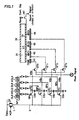
- Fig. 1 is a circuit diagram of the liquid crystal display device of the first embodiment. Although only a single pixel is shown in the figure for simplification, a plurality of the pixels is arranged in a matrix in the display device.
- a digital image signal is serially transferred from a drain driver (not shown) and supplied to a drain signal line 2 through a transmission gate 1.
- Control clocks CP and *CP (*CP is an inverted clock of CP) control turning on and off of the transmission gate 1.
- Drains of pixel selecting transistors GT0 to GT3 are commonly connected to a drain signal line 2.
- Sampling pulses SP0 to SP3 for sampling a digital image signal at a predetermined timing are severally supplied to each gates of the pixel selecting transistors GT0 to GT3.
- sampling pulses SP0 to SP3 are generated by shift registers SR.
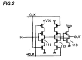
- the shift register SR includes clocked inverters 111 and 112 which are applied with shift clocks CLK and *CLK (*CLK is an inverted clock of CLK) and an inverter 113.
- the shift registers SR sequentially shift an input clock AP in response to the shift clocks CLK and *CLK, thereby providing the sampling pulses SP0 to SP3 from each stages of the shift registers SR.
- Sources of the pixel selecting transistors GT0 to GT3 are connected to capacitors CS0 to CS3 for retaining each bit data of a digital image signal written in through the pixel selecting transistors GT0 to GT3.
- the bit data retained in the capacitors CS0 to CS3 are severally supplied to gates of clock supplying transistors ST0 to ST3 which are provided at the next stage.
- Sources of the clock supplying transistors ST0 to ST3 are supplied with pixel signals (periodic clocks).
- Drains of the clock supplying transistors ST0 to ST3 are connected to capacitor electrodes 41, 42, 43, and 44, which are coupled to the pixel electrode 19 through capacitance coupling.
- capacitors C0, C1, C2, and C3 are formed between the pixel electrode 19 and the capacitor electrodes 41, 42, 43, and 44.
- a liquid crystal 21 is filled between the pixel electrode 19 and a common electrode 32.
- the clock supplying transistors ST0 to ST3 turn on or off in response to each bit data of the digital image signal, which are supplied from the drain signal line 2 and retained at the capacitors CS0 to CS3 through the pixel selecting transistors GTO to GT3.
- a pixel signal is applied to the capacitor electrode 41 through the clock supplying transistor ST0. Accordingly, a voltage change ⁇ V occurs at the pixel electrode 19 in response to a voltage amplitude V P-P of the clock and a capacitance value C0.
- ⁇ V C0.V P-P / (CLC+C0)
- CLC is a value of capacitor between the pixel electrode 19 and the common electrode 32. Therefore, by assigning weights to the capacitors C0, C1, C2, and C3, corresponding to each bits of the digital image signals, a voltage of the corresponding analog image signal converted from the digital image signal is supplied to the pixel electrode 19.
- n0, n1, n2, and n3 are digital image signal data, and each of those is severally “1” or "0".
- the pixel electrode 19 is provided with a reset transistor RT for supplying a reset signal. This makes it possible to perform an inverting driving method in which an inverted voltage is alternately applied to the liquid crystal 21, as described later.
- Figs. 3 and 4 are timing charts of the liquid crystal display device. The operation of serial-to-parallel conversion will be described with reference to Fig. 3 first.
- the transmission gate 1 turns on so that digital image signal data is transmitted through the transmission gate 1 and supplied to the drain signal line 2 as serial data in time series.
- Each bit data of the digital image signal are sampled by the sampling pulses SP0 to SP3, converted to parallel data through the pixel selecting transistors GT0 to GT3, and retained at the capacitors CS0 to CS3.
- the digital image signal data of four bits (1, 0, 1, 0) are retained.
- the pixel signal is a signal which is supplied to the capacitor electrodes 41 to 44 through the transistors ST0 to ST3, alternating between 0V and 3V at a predetermined period.
- a reset control signal is a signal which is supplied to the gate of the reset transistor RT.
- the reset control signal is a pulse signal which turns to a high level immediately before the pixel signal is inverted.
- the common electrode 32 is fixed at a DC level of, for example, 3V.
- serial data of a digital image signal supplied to the drain signal line 2 is converted to, for example, four-bit parallel data (1, 0, 0, 0) by the described operation of the serial-to-parallel conversion. Then, among the capacitors CS0 to CS3, to which each data is supplied through the pixel selecting transistors GT0 to GT3, CS0 supplied with data of "1" is charged, and the CS1 to CS3 are discharged so that data (1, 0, 0, 0) are retained therein. Accordingly, the clock supplying transistor ST0 turns on and the clock supplying transistors ST1 to ST3 turn off, so that a pixel signal is applied to the capacitor electrode 41 through the clock supplying transistor ST0.
- a frame rate can be lowered to a minimum frequency required for refreshing the data at the data retaining portion, thereby reducing power consumption of the display device. Furthermore, since the DA converter is not provided in the periphery of the driver circuit but integrated in a pixel by capacitance coupling, the frame of the display device is narrower than the that of the conventional display device.
- the reset transistor RT turns on, resetting the voltage of the pixel electrode 19 to a potential equal to the potential of the common electrode 32, i.e., 3V.
- the voltage of the pixel signal changes from 3V to 0V. Accordingly, the voltage of the pixel electrode 19 is reduced from 3V by ⁇ V0 by capacitance coupling.
- the pixel electrode 19 changes its voltage, inverting the voltage around the voltage of the common electrode 32, thereby enabling the driving of the display device without degrading the liquid crystal 21.
- the cycle of refreshing the data at the data retaining portion can be independent of the cycle of inverting the pixel signal voltage, without any synchronization. For more reduction of the power consumption, it is preferable to set each of the cycles at the longest as long as the cycles severally satisfy necessity of refreshing the data at the data retaining portion and necessity of inverting the pixel signal for preventing degrading of the liquid crystal.
- the circuit is driven by refreshing the data, a noise can be generated in a picture by a parasitic capacitance between wiring lines in the circuits. Therefore, it is most preferable to synchronize the cycles and to set each of the cycles as long as possible.
- Fig. 5 is another timing chart of the liquid crystal display device. This figure also shows the timing of operating the AD conversion after conversion to parallel data.
- the common electrode 32 is AC-driven.
- the pixel signal is obtained by dividing frequencies of a standard clock and delaying those, and has voltage amplitudes of 0V and 3V. There is a difference in phase between common signal supplied to the common electrode 32 and the pixel signal.
- the reset transistor RT resets the voltage of the pixel electrode 19 at a level of a reset signal #1 or a reset signal #2 in response to a reset control signal.
- the reset signal #1 is selected.
- the reset signal #1 is a signal which changes before the changing of the common signal and immediately before or simultaneously with turning high of the reset control signal.
- the common electrode is at 0V, and when the reset control signal turns to a high level, the pixel electrode is reset at 2V.
- the pixel electrode 19 is driven to alternately invert its voltage with the voltage of the common electrode 32 as a standard.
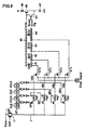
- Fig. 6 is a circuit diagram of the display device of the second embodiment. Although this figure shows a single pixel for simplification, a plurality of the pixels is arranged in a matrix in the display device.
- the same reference numerals as those of Fig. 1 are given to the same elements as those of Fig. 1, which are already described in the first embodiment, and the descriptions thereof are omitted here.
- static memory circuits 5 to 8 are provided, replacing the capacitors CS0 to CS3 for retaining the data provided in the first embodiment.
- the static memory circuits 5 to 8 each include two inverter circuits with positive feedback. Although it is necessary to refresh the data for retaining the data in the first embodiment, in this embodiment the data is retained by the static memory circuit without refreshing operation. Furthermore, for displaying a still picture, the data retained in the data retaining portion can be displayed as a still picture while stopping external circuits and each driver circuit. This makes it possible to lower the power consumption, comparing to the first embodiment. However, the number of elements increases and circuits are more complicated so that a larger area is required, comparing to the first embodiment. The operation of this display device is the same as that of the first embodiment, so that the description is omitted here.
- a semiconductor layer 11 made of polycrystalline silicon is formed like an island on one insulating substrate 10, and a gate insulating film 12 is formed on the semiconductor layer 11 and the insulating substrate 10.
- a gate electrode 13 is formed above the semiconductor layer 11 with the gate insulating film 12 interposed therebetween.
- a source 11s and a drain 11d are formed in the semiconductor layer 11 at both sides of the gate electrode 13.
- the TFT having such a configuration is used for the pixel selecting transistors GT0 to GT3 or the reset transistor RT.
- the configuration shown in this figure is for the reset transistor RT.
- An interlayer insulating film 14 is laminated on the gate electrode 13 and the gate insulating film 12.
- a contact hole 15 is formed in a position corresponding to the drain 11d, and the drain lid is connected to a drain electrode 16 through the contact hole 15.
- the source 11s is connected to the pixel electrode 19 through the contact hole 18 provided in the interlayer insulating film 14 and a planarization insulating film 17 provided on the interlayer insulating film 14.
- the capacitor electrodes 41, 42, and 43 made of Al (aluminum) are formed on the interlayer insulating film 14, away from the TFT.
- the capacitor electrodes 41, 42, and 43 are coupled to the pixel electrode 19 through capacitance coupling, thereby forming the capacitors C1, C2, and C3.
- the pixel electrode 19 formed on the planarization insulating film 17 is made of a reflective material such as Al.
- An alignment film 20, which aligns the liquid crystal 21 and is made of polyimide, is formed on the pixel electrode 19 and the planarization insulating film 17.
- a color filter which provides each colors of red (R), green (G) and blue (B), the common electrode 32 formed of a transparent conductive film made of, for example, ITO (indium tin oxide), and an alignment film 33, which aligns the liquid crystal 21, are formed on another insulating substrate 30 in this order.
- the color filter is unnecessary if a color picture is not to be displayed.
- the pair of the insulating substrates 10 and 30 thus formed is attached at its periphery with an adhesive sealing material.
- a space formed by the attached substrates is filled with the liquid crystal 21, completing the reflective liquid crystal display device.
- Fig. 8 shows another device configuration of the reflective liquid crystal display device for the embodiments described above.
- the pixel electrode 19 is connected to an electrode 19A provided on the interlayer insulating film 14 through a contact hole 18A provided in the planarization insulating film 17.
- the capacitor electrodes 41, 42, and 43 are formed on the gate insulating film 12. Accordingly, the capacitor electrodes 41, 42, and 43 are coupled to the pixel electrode 19 through the electrode 19A.
- Fig. 9 is a circuit diagram of the display device of the third embodiment. Although this figure shows a single pixel for simplification, the display device has a plurality of the pixels arranged in a matrix.
- the same reference numerals as those of Fig. 1 are given to the same elements as those of Fig. 1, which are described in the first embodiment, and the descriptions thereof are omitted here.
- the display device of the third embodiment is an electroluminescent display device.
- This embodiment is the same as the first and second embodiments in that a floating electrode 45 and a plurality of the capacitor electrodes 41 to 44 provided for the respective pixels are coupled to each other through capacitance coupling so that an electric potential of the floating electrode 45 changes.
- an EL driving transistor 46, a constant-current source 47, and an EL element 48 are provided in the display device.
- the EL element 48 is a light-emitting element emitting a light at luminance corresponding to the amount of an electric current flowing through the EL element 48.
- the floating electrode 45 is connected to a gate of the EL driving transistor 46.
- a threshold is set so that electrical conductivity changes in response to the potential of the floating electrode 45.
- the electric current corresponding to the electric potential of the floating electrode 45 is supplied from the constant-current source 47 to the EL element 48, and the EL element 48 emits a light at luminance corresponding to the current.
- This embodiment can be easily applied to a current-driven display device by replacing the EL element 48 by other light-emitting elements such as an LED.
- a DA converter for converting a digital image signal to an analog image signal is provided in a pixel, thereby simplifying a configuration of peripheral circuits of the pixel and reducing the frame area accordingly.
- the digital image signal data are serially transferred to each of the pixels from the outside, converted from serial signal data to parallel signal data, and then converted from digital signal data to analog signal data. Therefore, comparing to parallel transfer of the digital image signal data, the number of wirings used for data transfer and the area for wiring lines in each of the pixels can be reduced, thereby providing a high-definition display device displaying a multiple gray-scale image.
Landscapes
- Engineering & Computer Science (AREA)
- Physics & Mathematics (AREA)
- General Physics & Mathematics (AREA)
- Theoretical Computer Science (AREA)
- Computer Hardware Design (AREA)
- Crystallography & Structural Chemistry (AREA)
- Chemical & Material Sciences (AREA)
- Nonlinear Science (AREA)
- Mathematical Physics (AREA)
- Optics & Photonics (AREA)
- Control Of Indicators Other Than Cathode Ray Tubes (AREA)
- Liquid Crystal Display Device Control (AREA)
- Liquid Crystal (AREA)
- Devices For Indicating Variable Information By Combining Individual Elements (AREA)
Abstract
Description
Claims (10)
- A display device having a plurality of pixels, each of the pixels comprising:a serial-to-parallel converter converting a serial digital image signal supplied serially to the display device to a parallel digital image signal;a DA converter converting the parallel digital image signal to an analog image signal; anda pixel electrode (19) configured to receive the analog image signal.
- The display device of claim 1, wherein the serial-to-parallel converter comprises a drain signal line (2) supplied with the serial digital image signal, a plurality of pixel selecting transistors (GT0-GT3) connected to the drain signal line (2) and a plurality of shift registers (SR), each of the shift registers (SR) supplying a sampling pulse (SP0-SP3 to a gate of the corresponding pixel selecting transistor (GT0-GT3) for sampling the serial digital image signal at a predetermined timing.
- The display device of claim 1 or 2, wherein the DA converter comprises a plurality of capacitor electrodes (41-44) coupled with the pixel electrode (19), each of the capacitor electrodes (41-44) having a weighted capacitance ratio to couple with the pixel electrode (19), a clock supplying portion (ST0-ST3 supplying a periodic clock signal to the capacitor electrodes (41-44) in response to the parallel digital image signal.
- The display device of claim 3, wherein areas of the capacitor electrodes (41-44) are weighed to reflect corresponding bits of the parallel digital image signal.
- A display device comprising:a drain signal line (2) configured to receive a serial digital image signal serially supplied to the display device;a plurality of pixel selecting transistors (GT0-GT3) connected to the drain signal line (2) and selecting a pixel of the display device;a plurality of shift registers (SR), each of the shift registers (SR) supplying a sampling pulse to a gate of the corresponding pixel selecting transistor (GT0-GT3) for sampling the serial digital image signal at a predetermined timing to produce a parallel digital image signal;a data retaining portion retaining the parallel digital image signal converted from the serial digital image signal;a pixel electrode (19) of the pixel;a plurality of capacitor electrodes (41-44) coupled with the pixel electrode (19), each of the capacitor electrodes (41-44) having a weighted capacitance ratio to couple with the pixel electrode (19); anda clock supplying portion (ST0-ST3) supplying a periodic clock signal to the capacitor electrodes (41-44) in response to the parallel digital image signal retained in the data retaining portion.
- The display device of claim 5, wherein areas of the capacitor electrodes (41-44) are weighed to reflect corresponding bits of the parallel digital image signal.
- The display device of claim 5 or 6, wherein the data retaining portion comprises a capacitor (CS0).
- The display device of claim 7, wherein the data retaining portion comprises at least one additional capacitor and the number of total capacitors (CS0-CS3) in the pixel corresponds to the number of bits of the parallel digital image signal.
- The display device of claim 5 or 6, wherein the data retaining portion comprises a static memory circuit (5).
- The display device of claim 9, wherein the data retaining portion comprises at least one additional static memory circuit and the number of total static memory circuits (5-8) in the pixel corresponds to the number of bits of the parallel digital image signal.
Applications Claiming Priority (2)
| Application Number | Priority Date | Filing Date | Title |
|---|---|---|---|
| JP2002216674A JP2004061624A (en) | 2002-07-25 | 2002-07-25 | Display device |
| JP2002216674 | 2002-07-25 |
Publications (2)
| Publication Number | Publication Date |
|---|---|
| EP1385141A2 true EP1385141A2 (en) | 2004-01-28 |
| EP1385141A3 EP1385141A3 (en) | 2006-09-13 |
Family
ID=29997268
Family Applications (1)
| Application Number | Title | Priority Date | Filing Date |
|---|---|---|---|
| EP03016964A Withdrawn EP1385141A3 (en) | 2002-07-25 | 2003-07-25 | Pixel driver circuit for liquid crystal display or electroluminescent display |
Country Status (6)
| Country | Link |
|---|---|
| US (1) | US7164404B2 (en) |
| EP (1) | EP1385141A3 (en) |
| JP (1) | JP2004061624A (en) |
| KR (2) | KR100567306B1 (en) |
| CN (1) | CN1246724C (en) |
| TW (1) | TW583447B (en) |
Cited By (1)
| Publication number | Priority date | Publication date | Assignee | Title |
|---|---|---|---|---|
| US8624801B2 (en) | 2006-01-19 | 2014-01-07 | Chimei Innolux Corporation | Pixel structure having a transistor gate voltage set by a reference voltage |
Families Citing this family (4)
| Publication number | Priority date | Publication date | Assignee | Title |
|---|---|---|---|---|
| TWI276031B (en) * | 2002-03-01 | 2007-03-11 | Semiconductor Energy Lab | Display device, light emitting device, and electronic equipment |
| US7088326B2 (en) * | 2003-04-22 | 2006-08-08 | Toppoly Optoelectronics Corp. | Single pixel driver for transflective LCD |
| KR100771353B1 (en) | 2005-08-16 | 2007-10-29 | 엡슨 이미징 디바이스 가부시키가이샤 | Digital analog conversion circuit |
| KR100662977B1 (en) * | 2005-10-25 | 2006-12-28 | 삼성에스디아이 주식회사 | Shift register and organic light emitting display device using same |
Family Cites Families (24)
| Publication number | Priority date | Publication date | Assignee | Title |
|---|---|---|---|---|
| JP2645036B2 (en) * | 1987-10-31 | 1997-08-25 | 株式会社東芝 | Electronic device and display data transfer method |
| JPH01193716A (en) | 1988-01-29 | 1989-08-03 | Hitachi Ltd | Liquid crystal display device |
| US4996523A (en) * | 1988-10-20 | 1991-02-26 | Eastman Kodak Company | Electroluminescent storage display with improved intensity driver circuits |
| US5767828A (en) * | 1995-07-20 | 1998-06-16 | The Regents Of The University Of Colorado | Method and apparatus for displaying grey-scale or color images from binary images |
| EP0797182A1 (en) | 1996-03-19 | 1997-09-24 | Hitachi, Ltd. | Active matrix LCD with data holding circuit in each pixel |
| JPH10153986A (en) * | 1996-09-25 | 1998-06-09 | Toshiba Corp | Display device |
| JP3780531B2 (en) * | 1997-06-30 | 2006-05-31 | セイコーエプソン株式会社 | VIDEO SIGNAL PROCESSING CIRCUIT, VIDEO DISPLAY DEVICE USING THE SAME, ELECTRONIC DEVICE, AND DIGITAL-ANALOG CONVERTER OUTPUT ADJUSTMENT METHOD |
| KR100430091B1 (en) | 1997-07-10 | 2004-07-15 | 엘지.필립스 엘시디 주식회사 | Liquid Crystal Display |
| US5952948A (en) * | 1997-09-24 | 1999-09-14 | Townsend And Townsend And Crew Llp | Low power liquid-crystal display driver |
| GB2333174A (en) * | 1998-01-09 | 1999-07-14 | Sharp Kk | Data line driver for an active matrix display |
| JP3483759B2 (en) * | 1998-03-19 | 2004-01-06 | 株式会社東芝 | Liquid crystal display |
| JP4161484B2 (en) * | 1999-10-15 | 2008-10-08 | セイコーエプソン株式会社 | Electro-optical device drive circuit, electro-optical device, and electronic apparatus |
| JP2001281635A (en) | 2000-03-30 | 2001-10-10 | Mitsubishi Electric Corp | Liquid crystal display |
| JP4201070B2 (en) | 2000-06-28 | 2008-12-24 | エルジー ディスプレイ カンパニー リミテッド | Apparatus and method for correcting gamma voltage of liquid crystal display device |
| KR100760932B1 (en) | 2000-12-29 | 2007-09-21 | 엘지.필립스 엘시디 주식회사 | LCD Display |
| TW518552B (en) | 2000-08-18 | 2003-01-21 | Semiconductor Energy Lab | Liquid crystal display device, method of driving the same, and method of driving a portable information device having the liquid crystal display device |
| US7184014B2 (en) * | 2000-10-05 | 2007-02-27 | Semiconductor Energy Laboratory Co., Ltd. | Liquid crystal display device |
| KR200221346Y1 (en) * | 2000-12-08 | 2001-04-16 | 송기원 | A damper for an exhaust hood |
| KR200226801Y1 (en) * | 2001-01-10 | 2001-06-15 | 최동식 | A power supply circuit |
| US6731272B2 (en) * | 2001-01-22 | 2004-05-04 | Intel Corporation | Pseudo static memory cell for digital light modulator |
| US6731257B2 (en) * | 2001-01-22 | 2004-05-04 | Brillian Corporation | Image quality improvement for liquid crystal displays |
| US6747623B2 (en) * | 2001-02-09 | 2004-06-08 | Semiconductor Energy Laboratory Co., Ltd. | Liquid crystal display device and method of driving the same |
| JP2002311901A (en) * | 2001-04-11 | 2002-10-25 | Sanyo Electric Co Ltd | Display device |
| JP4067878B2 (en) * | 2002-06-06 | 2008-03-26 | 株式会社半導体エネルギー研究所 | Light emitting device and electric appliance using the same |
-
2002
- 2002-07-25 JP JP2002216674A patent/JP2004061624A/en active Pending
-
2003
- 2003-06-19 TW TW092116624A patent/TW583447B/en not_active IP Right Cessation
- 2003-07-24 CN CNB031503306A patent/CN1246724C/en not_active Expired - Fee Related
- 2003-07-24 US US10/625,843 patent/US7164404B2/en not_active Expired - Fee Related
- 2003-07-24 KR KR1020030050922A patent/KR100567306B1/en not_active Expired - Fee Related
- 2003-07-25 EP EP03016964A patent/EP1385141A3/en not_active Withdrawn
-
2006
- 2006-02-17 KR KR1020060015440A patent/KR100597912B1/en not_active Expired - Fee Related
Cited By (1)
| Publication number | Priority date | Publication date | Assignee | Title |
|---|---|---|---|---|
| US8624801B2 (en) | 2006-01-19 | 2014-01-07 | Chimei Innolux Corporation | Pixel structure having a transistor gate voltage set by a reference voltage |
Also Published As
| Publication number | Publication date |
|---|---|
| KR100567306B1 (en) | 2006-04-04 |
| CN1246724C (en) | 2006-03-22 |
| TW583447B (en) | 2004-04-11 |
| KR20060021408A (en) | 2006-03-07 |
| US7164404B2 (en) | 2007-01-16 |
| KR100597912B1 (en) | 2006-07-10 |
| US20040212556A1 (en) | 2004-10-28 |
| KR20040010369A (en) | 2004-01-31 |
| TW200401913A (en) | 2004-02-01 |
| EP1385141A3 (en) | 2006-09-13 |
| JP2004061624A (en) | 2004-02-26 |
| CN1479150A (en) | 2004-03-03 |
Similar Documents
| Publication | Publication Date | Title |
|---|---|---|
| US10692439B2 (en) | OLED display panel and OLED display device | |
| US11308872B2 (en) | OLED display panel for minimizing area of internalconnection line part for connecting GIP dirving circuit located in active area and OLED display device comprising the same | |
| KR100481099B1 (en) | Display device | |
| US20210327357A1 (en) | Pixel circuit and method for driving the same, and display panel | |
| KR20210047436A (en) | Display device | |
| CN216119516U (en) | Pixel circuit, display panel and display device | |
| US20080055300A1 (en) | Electrooptic device, driving circuit, and electronic device | |
| JPH11271713A (en) | Liquid crystal display | |
| US7312638B2 (en) | Scanning line driving circuit, display device, and electronic apparatus | |
| US7123233B2 (en) | Display device | |
| US7173589B2 (en) | Display device | |
| JP2012088736A (en) | Display device | |
| KR102819288B1 (en) | Backlight driver, backlight device including the same and operationg method of the backlight device | |
| US7164404B2 (en) | Display device | |
| JP2002251160A (en) | Display device | |
| KR102467881B1 (en) | OLED display Panel | |
| JP2002162948A (en) | Display device and driving method thereof | |
| US8558828B2 (en) | Electrooptic device, driving circuit, and electronic device | |
| JP2001056662A (en) | Flat panel display | |
| JP2001183998A (en) | Display device | |
| CN119964519A (en) | Gate driving circuit and display device | |
| JP2008040202A (en) | Electrooptical device, driving circuit, and electronic equipment |
Legal Events
| Date | Code | Title | Description |
|---|---|---|---|
| PUAI | Public reference made under article 153(3) epc to a published international application that has entered the european phase |
Free format text: ORIGINAL CODE: 0009012 |
|
| AK | Designated contracting states |
Kind code of ref document: A2 Designated state(s): AT BE BG CH CY CZ DE DK EE ES FI FR GB GR HU IE IT LI LU MC NL PT RO SE SI SK TR |
|
| AX | Request for extension of the european patent |
Extension state: AL LT LV MK |
|
| PUAL | Search report despatched |
Free format text: ORIGINAL CODE: 0009013 |
|
| AK | Designated contracting states |
Kind code of ref document: A3 Designated state(s): AT BE BG CH CY CZ DE DK EE ES FI FR GB GR HU IE IT LI LU MC NL PT RO SE SI SK TR |
|
| AX | Request for extension of the european patent |
Extension state: AL LT LV MK |
|
| AKX | Designation fees paid | ||
| STAA | Information on the status of an ep patent application or granted ep patent |
Free format text: STATUS: THE APPLICATION IS DEEMED TO BE WITHDRAWN |
|
| 18D | Application deemed to be withdrawn |
Effective date: 20070314 |
|
| REG | Reference to a national code |
Ref country code: DE Ref legal event code: 8566 |