EP1381852B1 - Matrix aus biosensoren und verfahren zu deren herstellung - Google Patents
Matrix aus biosensoren und verfahren zu deren herstellung Download PDFInfo
- Publication number
- EP1381852B1 EP1381852B1 EP02730368A EP02730368A EP1381852B1 EP 1381852 B1 EP1381852 B1 EP 1381852B1 EP 02730368 A EP02730368 A EP 02730368A EP 02730368 A EP02730368 A EP 02730368A EP 1381852 B1 EP1381852 B1 EP 1381852B1
- Authority
- EP
- European Patent Office
- Prior art keywords
- substrate
- layer
- piezoresistive
- sensing elements
- matrix
- Prior art date
- Legal status (The legal status is an assumption and is not a legal conclusion. Google has not performed a legal analysis and makes no representation as to the accuracy of the status listed.)
- Expired - Lifetime
Links
Images

Classifications
-
- G—PHYSICS
- G01—MEASURING; TESTING
- G01N—INVESTIGATING OR ANALYSING MATERIALS BY DETERMINING THEIR CHEMICAL OR PHYSICAL PROPERTIES
- G01N29/00—Investigating or analysing materials by the use of ultrasonic, sonic or infrasonic waves; Visualisation of the interior of objects by transmitting ultrasonic or sonic waves through the object
- G01N29/02—Analysing fluids
- G01N29/036—Analysing fluids by measuring frequency or resonance of acoustic waves
-
- B—PERFORMING OPERATIONS; TRANSPORTING
- B01—PHYSICAL OR CHEMICAL PROCESSES OR APPARATUS IN GENERAL
- B01L—CHEMICAL OR PHYSICAL LABORATORY APPARATUS FOR GENERAL USE
- B01L3/00—Containers or dishes for laboratory use, e.g. laboratory glassware; Droppers
- B01L3/50—Containers for the purpose of retaining a material to be analysed, e.g. test tubes
- B01L3/508—Rigid containers without fluid transport within
- B01L3/5085—Rigid containers without fluid transport within for multiple samples, e.g. microtitration plates
-
- B—PERFORMING OPERATIONS; TRANSPORTING
- B81—MICROSTRUCTURAL TECHNOLOGY
- B81B—MICROSTRUCTURAL DEVICES OR SYSTEMS, e.g. MICROMECHANICAL DEVICES
- B81B3/00—Devices comprising flexible or deformable elements, e.g. comprising elastic tongues or membranes
- B81B3/0018—Structures acting upon the moving or flexible element for transforming energy into mechanical movement or vice versa, i.e. actuators, sensors, generators
-
- B—PERFORMING OPERATIONS; TRANSPORTING
- B01—PHYSICAL OR CHEMICAL PROCESSES OR APPARATUS IN GENERAL
- B01J—CHEMICAL OR PHYSICAL PROCESSES, e.g. CATALYSIS OR COLLOID CHEMISTRY; THEIR RELEVANT APPARATUS
- B01J2219/00—Chemical, physical or physico-chemical processes in general; Their relevant apparatus
- B01J2219/00274—Sequential or parallel reactions; Apparatus and devices for combinatorial chemistry or for making arrays; Chemical library technology
- B01J2219/00277—Apparatus
- B01J2219/00279—Features relating to reactor vessels
- B01J2219/00306—Reactor vessels in a multiple arrangement
- B01J2219/00313—Reactor vessels in a multiple arrangement the reactor vessels being formed by arrays of wells in blocks
- B01J2219/00315—Microtiter plates
- B01J2219/00317—Microwell devices, i.e. having large numbers of wells
-
- B—PERFORMING OPERATIONS; TRANSPORTING
- B01—PHYSICAL OR CHEMICAL PROCESSES OR APPARATUS IN GENERAL
- B01J—CHEMICAL OR PHYSICAL PROCESSES, e.g. CATALYSIS OR COLLOID CHEMISTRY; THEIR RELEVANT APPARATUS
- B01J2219/00—Chemical, physical or physico-chemical processes in general; Their relevant apparatus
- B01J2219/00274—Sequential or parallel reactions; Apparatus and devices for combinatorial chemistry or for making arrays; Chemical library technology
- B01J2219/00583—Features relative to the processes being carried out
- B01J2219/00585—Parallel processes
-
- B—PERFORMING OPERATIONS; TRANSPORTING
- B01—PHYSICAL OR CHEMICAL PROCESSES OR APPARATUS IN GENERAL
- B01J—CHEMICAL OR PHYSICAL PROCESSES, e.g. CATALYSIS OR COLLOID CHEMISTRY; THEIR RELEVANT APPARATUS
- B01J2219/00—Chemical, physical or physico-chemical processes in general; Their relevant apparatus
- B01J2219/00274—Sequential or parallel reactions; Apparatus and devices for combinatorial chemistry or for making arrays; Chemical library technology
- B01J2219/00583—Features relative to the processes being carried out
- B01J2219/00596—Solid-phase processes
-
- B—PERFORMING OPERATIONS; TRANSPORTING
- B01—PHYSICAL OR CHEMICAL PROCESSES OR APPARATUS IN GENERAL
- B01J—CHEMICAL OR PHYSICAL PROCESSES, e.g. CATALYSIS OR COLLOID CHEMISTRY; THEIR RELEVANT APPARATUS
- B01J2219/00—Chemical, physical or physico-chemical processes in general; Their relevant apparatus
- B01J2219/00274—Sequential or parallel reactions; Apparatus and devices for combinatorial chemistry or for making arrays; Chemical library technology
- B01J2219/00583—Features relative to the processes being carried out
- B01J2219/00603—Making arrays on substantially continuous surfaces
- B01J2219/00605—Making arrays on substantially continuous surfaces the compounds being directly bound or immobilised to solid supports
- B01J2219/00612—Making arrays on substantially continuous surfaces the compounds being directly bound or immobilised to solid supports the surface being inorganic
-
- B—PERFORMING OPERATIONS; TRANSPORTING
- B01—PHYSICAL OR CHEMICAL PROCESSES OR APPARATUS IN GENERAL
- B01J—CHEMICAL OR PHYSICAL PROCESSES, e.g. CATALYSIS OR COLLOID CHEMISTRY; THEIR RELEVANT APPARATUS
- B01J2219/00—Chemical, physical or physico-chemical processes in general; Their relevant apparatus
- B01J2219/00274—Sequential or parallel reactions; Apparatus and devices for combinatorial chemistry or for making arrays; Chemical library technology
- B01J2219/00583—Features relative to the processes being carried out
- B01J2219/00603—Making arrays on substantially continuous surfaces
- B01J2219/00653—Making arrays on substantially continuous surfaces the compounds being bound to electrodes embedded in or on the solid supports
-
- B—PERFORMING OPERATIONS; TRANSPORTING
- B01—PHYSICAL OR CHEMICAL PROCESSES OR APPARATUS IN GENERAL
- B01J—CHEMICAL OR PHYSICAL PROCESSES, e.g. CATALYSIS OR COLLOID CHEMISTRY; THEIR RELEVANT APPARATUS
- B01J2219/00—Chemical, physical or physico-chemical processes in general; Their relevant apparatus
- B01J2219/00274—Sequential or parallel reactions; Apparatus and devices for combinatorial chemistry or for making arrays; Chemical library technology
- B01J2219/00583—Features relative to the processes being carried out
- B01J2219/00603—Making arrays on substantially continuous surfaces
- B01J2219/00659—Two-dimensional arrays
-
- B—PERFORMING OPERATIONS; TRANSPORTING
- B01—PHYSICAL OR CHEMICAL PROCESSES OR APPARATUS IN GENERAL
- B01J—CHEMICAL OR PHYSICAL PROCESSES, e.g. CATALYSIS OR COLLOID CHEMISTRY; THEIR RELEVANT APPARATUS
- B01J2219/00—Chemical, physical or physico-chemical processes in general; Their relevant apparatus
- B01J2219/00274—Sequential or parallel reactions; Apparatus and devices for combinatorial chemistry or for making arrays; Chemical library technology
- B01J2219/0068—Means for controlling the apparatus of the process
- B01J2219/00702—Processes involving means for analysing and characterising the products
-
- C—CHEMISTRY; METALLURGY
- C40—COMBINATORIAL TECHNOLOGY
- C40B—COMBINATORIAL CHEMISTRY; LIBRARIES, e.g. CHEMICAL LIBRARIES
- C40B60/00—Apparatus specially adapted for use in combinatorial chemistry or with libraries
- C40B60/14—Apparatus specially adapted for use in combinatorial chemistry or with libraries for creating libraries
-
- G—PHYSICS
- G01—MEASURING; TESTING
- G01N—INVESTIGATING OR ANALYSING MATERIALS BY DETERMINING THEIR CHEMICAL OR PHYSICAL PROPERTIES
- G01N2291/00—Indexing codes associated with group G01N29/00
- G01N2291/02—Indexing codes associated with the analysed material
- G01N2291/025—Change of phase or condition
- G01N2291/0256—Adsorption, desorption, surface mass change, e.g. on biosensors
Definitions
- the present invention relates to a biosensor matrix using the piezoresistive effect or the piezoelectric effect for the detection of specific molecular interaction. It also relates to its manufacturing process.
- the invention proposes a technique for integrating on a single semiconductor substrate a large number of biosensors.
- the invention thus relates to a biosensor matrix capable of detecting specific interactions of oligonucleotides (DNA / DNA, DNA / RNA) or proteins (DNA / proteins) or of antibody antigens and comprising a substrate made of a semiconductor material, characterized in that it has a planar main surface (4) as well as open cavities (8) formed from a plane surface (10) opposite to said planar surface (4) and each having a deformable structure (40, 50) having a plurality of sensitive elements which are piezoresistors (44) or piezoelectric elements (54) disposed between the bottom (9, 9 1 ) of said cavities (8) and the flat surface (4), and which are mounted in Wheatstone bridge.
- These cavities are thus open cavities that open onto the surface opposite to the main plane surface.
- At least one deformable structure is a membrane.
- a deformable structure may comprise at least one beam embedded in one or preferably two ends, for example by implementing a localized surface attack.
- the substrate may be of silicon, and preferentially be of a type having a buried SiO 2 layer (SOI substrate).
- At least one deformable structure integrates at least one piezoresistive sensitive element.
- At least one deformable structure has at least one piezoelectric sensitive element deposited on the substrate.
- the plane surface advantageously has metallizations.
- this layer of SiO 2 can be completely removed.
- Step a 31 is preferably preceded by a pre-morphing of the surface of the substrate at said first localized locations of the masking layer, for example by implantation of germanium.
- the method implements the production of electrical contact electrodes for the piezoresistive sensitive elements.
- the sensitive elements are piezoelectric and step a comprises depositing on said first localized locations a piezoelectric layer followed by a crystallization annealing.
- the method advantageously implements the realization of electrical contacting electrodes for the piezoelectric sensitive elements.
- the invention relates to the field of genomics, proteomics (DNA chips, protein chips) and more generally biochips. It relates to a device for the detection of specific interactions, oligonucleotides (DNA / DNA, DNA / RNA) or proteins (DNA / proteins) or antigen-antibodies.
- Such a system makes it possible to dispense with probe labeling techniques and thus external detection systems by fluorescence or radioactivity.
- the proposed detection principle can be compared to that of quartz crystal microbalances in which a variation in the mass induces a variation of the resonant frequency and / or the damping of the resonance structure.
- the implementation in the context of the invention of thin sensitive elements of piezoelectric or preferably piezoresistive type improves the performance and especially the sensitivity compared to quartz crystal microbalances, for which the Q quality must be very high so that the sensitivity is sufficient.
- the mass variations to be detected are consecutive to the pairing of target DNAs (or RNA, proteins or any type of interaction between molecules) with the DNA probes present on the surface. sensitive element.
- the technique according to the invention makes it possible to implement on the same substrate a multitude of resonant structures independent of reduced dimensions, for example a few microns, and no longer a single device as is the case in the prior art.
- This approach is possible because ultra-thin piezoresistance techniques or ultra-thin piezoelectric layers are compatible with silicon technologies, making it possible to manufacture resonant microstructures collectively and at low cost.
- the piezoresistive sensitive elements in particular membranes, are preferably used. This has two advantages:
- the proposed system further allows, in static during the deposition phase, if one uses contact deposition systems, to know the force and the time of support of the needles on the devices where the deposits take place. If a non-contact deposition system (microfluidic system with ejection of drops) is used, the system according to the invention makes it possible to know the quantity of liquid deposited, the mass of the drop inducing a variation of the stress and therefore a variation of the piezoresistance (or a piezoelectric effect).
- This possibility of detection is important because it conditions the quality of the deposits (volume and thus concentration deposited, and the reliability of the results).
- This system is compatible with an active control of the deposition with feedback loop to correct the errors as a function of the force and the contact time during the deposit.
- the method can be used to calibrate contact deposition systems by adjusting the height of the tips, checking wear and mechanical drift effects of the system or even parasitic interaction effects such as vibrations, or good for calibrating non-contact deposition systems to adjust the drop ejection frequency or even the distance between the ejection area and the surface of the microdevice.
- Such a calibration device can be used before or after a series of deposits in the case of a contact system, and after filing in the case of a contactless system.
- the membranes make it possible to ensure an effective mechanical decoupling between the different resonant monodispositives.
- This dynamic mode can also be used for the deposition phase in the same way as previously described under point 1 / to control the quality of the deposits.
- the invention implements a localized preamplification of the substrate followed by an implantation of boron or boron fluoride especially at very low energy, for example 15keV, associated with rapid thermal annealing. For example, annealing for 1 to 10 seconds between 900 and 1100 ° C provide the desired results.
- the membranes are for example of monocrystalline silicon, of uniform thickness (a few microns to a few hundred microns) of orientation (100) and have edges parallel to directions ⁇ 110>.
- the substrate is for example of the type n dosed at 10 17 atoms / cm 3 .
- the piezoresistances (or piezoresistive gauges) whose nominal value is of the order of 1 k ⁇ to 10 k ⁇ (typically a few k ⁇ for example between 4 and 4.5 k ⁇ ) are implanted to give them doping, in particular P + , between 18 and 10 19 atoms / cm 3 .
- the length of these gauges is between 50 microns and a few hundred microns (for example 50 ⁇ and 500 ⁇ ) and their width is between 10 microns and a few tens of microns (for example between 10 ⁇ and 50 ⁇ or 100 ⁇ ).
- the thickness h of the membrane is for example between 2 and 30 ⁇ and is for example equal to 15 ⁇ .
- a Wheatstone bridge circuit compensates for the thermal drift of the resistor by rejecting the common mode.
- a reduction in the size of the gauges makes it possible to optimize the average stress seen by the gauge and therefore the sensitivity. This reduction must be related to the tolerances of the manufacturing process used, so as not to unduly increase the dispersion of the values of the gauges.
- the senor can be calibrated by measuring the voltage variations collected at the Wheatstone bridge terminals when calibrated forces are applied to the diaphragm.
- the technique described has the advantage of leading to beam-shaped piezoresistive sensors which have a very much improved sensitivity compared to those obtained by the techniques. These improvements are due to the fact that the combination of the two abovementioned techniques (preamorphization and implantation) associated with rapid thermal annealing techniques makes it possible to perfectly confine the piezoresistive zone on the surface of the device where the mechanical stress is maximum during the deflection, whether in static or dynamic mode.
- the advantage of the technique of the invention is to obtain piezoresistances having a very low junction depth, especially between 50 nm and 200 nm, or between 50 nm and 100 nm and, for example equal to 70 nm, with a conventional Si starting substrate for example doped at 10 17 per cm 3 , in which the boron is implanted with an energy of 15keV.
- a boron implantation followed by a conventional annealing can give junction depths of 0.3 to 0.4 ⁇ m.
- This technique of ultra-thin piezoresistrance development combining a low-energy boron or low-energy BF2 pre-morphing with fast thermal annealing, can be used for the fabrication of membranes incorporating piezoresistive sensors as well as piezoresistive levers in the framework of the present invention (perfectly adapted also to atomic force microscopy).
- a matrix of biosensors comprising membranes for example of thickness 5 microns integrating four piezoresistors mounted bridge WHEATSTONE.
- a gold pad for example 200 microns in diameter, appropriately insulated from the plugs electrical contact, which allows to locate the molecular interactions (chemical interaction on gold with a specific grafting chemistry for gold).
- the mechanical vacuum resonances (fundamental mode) of the microdevices can be measured electrically via the variations of the piezoresistances.
- a calibration protocol makes it possible to measure the resonant frequency variation following the pairing of complementary DNA strands, the antibody, DNA / protein antigen interaction, etc.
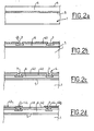
- a matrix of biosensors according to the invention is represented at figure 1a . It has a two-dimensional network of biosensors each of which is composed of a membrane 2 and a plurality of piezoresistive or piezoelectric sensitive elements. As shown more particularly in figure 1b , the sensitive elements referenced 3 1 , 3 2 , 3 3 and 3 4 are arranged to allow detection when connected WHEATSTONE bridge.
- Each of the membranes 2 is delimited between the plane main face referenced 4 of the substrate 1 and the bottom 9 of the open cavity at its upper part (in its use configuration which is inverted with respect to that shown to illustrate the method of manufacture), which is carried out in the substrate (see figure 2e ).
- the gauges R1 to R4 having the same resistance are located in the middle of each edge of a square (or rectangular) membrane of side a, so that the gauges are in the zones of maximum stress and the responses of the gauges are in identical absolute value.
- the variations of the resistances R2 and R4 on the one hand and R1 and R3 on the other hand have opposite signs, whence the electrical assembly of the Wheatstone bridge to the figure 1d . This configuration minimizes the thermodynamic stresses generated by the interconnections for the membrane.
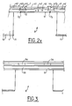
- a manufacturing process for the implementation of piezoresistive sensitive elements will now be described in connection with the Figures 2a to 2f from a starting substrate 1 which has a buried layer 5 made of SiO 2 surmounted by a surface layer 6 whose thickness is a few microns (for an SOI type substrate), and which may be less than one micron for a SIMOX type substrate.
- a layer of oxide 41 is deposited on the surface of the substrate in which openings 45 are made which will make it possible to produce the piezoresistances.
- a first (optional) implantation of germanium is firstly performed to pre-amalgamate locally the surface layer 6.
- boron B or BF 2 is implanted at a density of 10 14 per cm 2 (for example to produce the zones 7 constituting the piezoresistances).
- a rapid thermal annealing lasting from a few seconds to a few seconds between 900 and 1100 ° C, this rapid treatment being optionally followed by a conventional annealing at a lower temperature, for example for 20 minutes at 800 ° C., the combination of these treatments making it possible to electrically activate the implanted boron (or BF 2) atoms and reduce the defects created during implantation ionic.
- the substrate is then passivated ( Figure 2c ) by depositing an oxide layer 42, for example a plasma chemical vapor-type cold deposition ("PECVD” or "LPCVD”).
- PECVD plasma chemical vapor-type cold deposition
- An aluminum metallization is then carried out to form electrical conductors 43 1 and 43 2 to take the contacts 44 on the piezoresistive sensitive elements 7 ( figure 2d ).
- open cavities 8 are made by deep dry ionic etching after masking by a thick resin layer 11.
- TMAH ammonium hydroxide tetramethyl
- KOH potassium hydroxide tetramethyl
- EDP ethylene diamine pyrocatechol
- the interfacial silicon oxide layer 5 of the substrate 1 serves as a stop layer for etching.
- This layer 5 is then optionally removed by RIE dry etching on the rear face, which is recommended rather than the use a chemical solution of fluoridic acid that may damage the front of the device.
- Each open cavity or dish 8 then has a thin membrane 40 incorporating piezoresistances 3 1 to 3 4 or R 1 to R 4 (corresponding to zones 44).
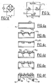
- a variant of the process is shown in relation to the Figures 4a to 4f .
- the implantation of B or BF 2 is carried out through openings 45 1 to produce the piezoresistances 7 1 ( figure 4b ).
- This implantation is followed by implantation annealing and thermal oxidation to isolate the resistors (41 1 , 42 1 , figure 4c ).
- Apertures are then made in the oxide layer 41 1 , 42 1 to make the contacts 44 1 by metallization Al, then the contacts are etched and the Al is annealed so as to obtain the metallizations (43 11 , 43 22 ) ( figure 4d ).
- a resin layer 1, which is insulated, is then opened to open the backside 41 2 oxide ( figure 4e ).
- a deep dry etching is performed on the rear face to form the open cavities 81 and the membranes 40 1 ( figure 4f ).
- the cavities 81 square or rectangular
- the steps of this method are carried out in the same way as for the process of the Figures 2a to 2c except that the substrate is Si without buried oxide layer.
- the proposed configuration adapts to any robotized system of depositing samples for depositing drops whose volume does not exceed a few nanoliters.
- contact deposition systems using microneedles or using piezoelectric systems are suitable.
- the biosensor matrix makes it possible to design an integrated detection system based on the fine measurement of mass variation resulting from hybridization or interaction between biological molecules by means of a piezoresistive or piezoelectric system disposed on a membrane (or on a beam).
- This device makes it possible to obtain from a qualitative point of view the detection of interactions between biological molecules, and from a quantitative point of view a measure of the quantity of molecules that have interacted, as well as a follow-up of the kinetics of reaction. this without resorting to steps of marking the biological molecules using radioactive or fluorescent markers.
- micro and nanotechnology allows mass and low cost production of the biosensor matrix. Given the principle of measuring mass variation, the molecules do not require prior labeling.
- the use of these sensors allows rapid and quantitative detection as well as real-time monitoring of the kinetics of the intermolecular reaction.
- the reduction in size of the resonant devices that makes it possible to obtain the technique used makes it possible to obtain a high resonance frequency, typically several MHz, with a high quality factor leading to an increase in sensitivity.
- the low mass of the active part of the microdevices makes them all the more sensitive to the slightest mass variation following the pairing of a complementary species.
- the measurements can be carried out in vacuum, and in this case washing and drying steps are used after hybridization. They can also be performed in a liquid medium, and in this case, the drying step is not performed.
- the biosensor matrix comprises a large number of resonant structures, it is possible to perform statistical analysis of the data if the same deposition is performed on each structure or to work simultaneously with several types of deposition.
- the invention can also be implemented by performing, by a method known per se, piezoelectric sensitive elements 54 arranged at localized locations on the main surface of the substrate (see FIG. figure 3 ).
- the open cavities 8 are then made as indicated above, to form deformable structures 40 (membrane, or beam embedded at one or two ends).
Landscapes
- Chemical & Material Sciences (AREA)
- Analytical Chemistry (AREA)
- Health & Medical Sciences (AREA)
- Physics & Mathematics (AREA)
- General Health & Medical Sciences (AREA)
- Pathology (AREA)
- Engineering & Computer Science (AREA)
- Life Sciences & Earth Sciences (AREA)
- General Physics & Mathematics (AREA)
- Immunology (AREA)
- Acoustics & Sound (AREA)
- Hematology (AREA)
- Clinical Laboratory Science (AREA)
- Chemical Kinetics & Catalysis (AREA)
- Biochemistry (AREA)
- Computer Hardware Design (AREA)
- Microelectronics & Electronic Packaging (AREA)
- Micromachines (AREA)
- Investigating Or Analysing Biological Materials (AREA)
- Pressure Sensors (AREA)
- Photometry And Measurement Of Optical Pulse Characteristics (AREA)
- Measuring Or Testing Involving Enzymes Or Micro-Organisms (AREA)
- Apparatus Associated With Microorganisms And Enzymes (AREA)
Claims (17)
- Biosensormatrix, die zur Detektion von spezifischen Wechselwirkungen von Oligonucleotiden (DNA/DNA; DNA/RNA) oder Proteinen (DNA/Proteinen) oder von Antigenen-Antikörpern fähig ist und ein Substrat aus Halbleitermaterial umfasst, dadurch gekennzeichnet, dass sie eine flache Hauptoberfläche (4) sowie offene Kavitäten (8) aufweist, welche ausgehend von einer flachen Oberfläche (10), die der flachen Oberfläche (4) gegenüberliegt, angeordnet sind und von denen jede eine verformbare Struktur (40, 50) aufweist, die eine Vielzahl von empfindlichen Elementen zeigt, die piezoelektrische Widerstände (44) oder piezoelektrische Elemente (54), die zwischen dem Boden (9, 91) der Kavitäten (8) und der flachen Oberfläche (4) angeordnet sind und die als Wheatstone-Brücke montiert sind, sind.
- Matrix gemäß Anspruch 1, dadurch gekennzeichnet, dass wenigstens eine verformbare Struktur eine Membran (40, 50) ist.
- Matrix gemäß einem der Ansprüche 1 oder 2, dadurch gekennzeichnet, dass wenigstens eine verformbare Struktur wenigstens einen Träger umfasst.
- Matrix gemäß Anspruch 2, dadurch gekennzeichnet, dass die piezoelektrischen Widerstände den selben Widerstand haben und sich in der Mitte jedes Randes einer quadratischen oder rechteckigen Membran befinden.
- Matrix gemäß einem der vorangehenden Ansprüche, dadurch gekennzeichnet, dass das Substrat aus Silicium ist.
- Matrix gemäß Anspruch 5, dadurch gekennzeichnet, dass das Substrat eine vertiefte Schicht (5) aus SiO2 aufweist.
- Matrix gemäß einem der vorangehenden Ansprüche, dadurch gekennzeichnet, dass die flache Hauptoberfläche (4) Metallisierungen (431, 432) aufweist, die die elektrische Verbindung der empfindlichen Elemente (44, 54) erlauben.
- Verfahren zur Herstellung einer Biosensormatrix gemäß einem der vorangehenden Ansprüche, dadurch gekennzeichnet, dass es durchführt:a) Herstellung der empfindlichen Elemente (44, 54) an ersten Stellen, die an der flachen Hauptoberfläche des Substrats lokalisiert sind,b) Herstellung der Kavitäten (8) ausgehend von zweiten Orten, die an einer zweiten Oberfläche (10) des Substrats lokalisiert sind, die der flachen Hauptoberfläche (4) gegenüberliegt, um verformbare Strukturen (40, 50) zu erhalten, die wenigstens ein empfindliches Element (44, 54) umfassen.
- Verfahren gemäß Anspruch 8, dadurch gekennzeichnet, dass die empfindlichen Elemente (44) piezoresistiv sind, dass das Substrat aus Silicium ist und a umfasst:a1) Abscheidung einer Maskierungsschicht (41) auf einer ersten Oberfläche des Substrats,a2) Herstellung von Öffnungen (45) an ersten Stellen, die in der Maskierungsschicht (41) lokalisiert sind,a3) Implantierung von Ionen im Hinblick auf die Herstellung der empfindlichen piezoresistiven Elemente (44),und dass b umfasst:b1) Abscheidung einer Maskierungsschicht (11) auf der zweiten Oberfläche (10) des Substrats, die der ersten Oberfläche gegenüberliegt,b2) Herstellung von Öffnungen an den zweiten Stellen, die in der Maskierungsschicht (11) lokalisiert sind,b3) Herstellung der Kavitäten (8) durch chemischen Angriff.
- Verfahren gemäß Anspruch 9, dadurch gekennzeichnet, dass das Substrat eine vertiefte Schicht (5) aus Siliciumdioxid umfasst, die von einer monokristallinen Oberflächenschicht (6) überdeckt wird, und dass a1 die Abscheidung der Maskierungsschicht (41) auf der Oberfläche der monokristallinen Oberflächenschicht (6), welche die erste Oberfläche des Substrats bildet, umfasst, und dass in b3 der Angriff wenigstens bis zur tieferliegenden Schicht aus Siliciumdioxid (5), die eine Stoppschicht bildet, fortgesetzt wird.
- Verfahren gemäß einem der Ansprüche 9 oder 10, dadurch gekennzeichnet, dass a3 durchführt:a31) eine Implantierung von Bor oder BF2,a32) Glühen.
- Verfahren gemäß Anspruch 11, dadurch gekennzeichnet, dass a31 eine Voramorphisierung der Oberfläche des Substrats an den Stellen, die in der Maskierungsschicht lokalisiert sind, vorausgeht.
- Verfahren gemäß Anspruch 12, dadurch gekennzeichnet, dass die Voramorphisierung durch Implantierung von Ge erfolgt.
- Verfahren gemäß einem der Ansprüche 9 bis 13, dadurch gekennzeichnet, dass es die Herstellung von Elektroden (431, 432) für den elektrischen Kontakt für die empfindlichen piezoresistiven Elemente (44) durchführt.
- Verfahren gemäß Anspruch 8, dadurch gekennzeichnet, dass die empfindlichen Elemente piezoelektrisch sind und dass a umfasst: die Abscheidung einer piezoelektrischen Schicht (54) an den ersten Orten, gefolgt von einem Kristallisationsglühen.
- Verfahren gemäß Anspruch 15, dadurch gekennzeichnet, dass es die Herstellung von Elektroden für den elektrischen Kontakt für die empfindlichen piezoelektrischen Elemente durchführt.
- Verfahren der Verwendung einer Biosensormatrix gemäß einem der Ansprüche 1 bis 8, dadurch gekennzeichnet, dass es umfasst:a) eine vorangehende Stufe der Kontrolle der Auflagekraft, die durch eine Probenauftragungsvorrichtung auf jeden der Biosensoren und/oder der Dauer, während eine Auflagekraft durch die Probenauftragungsvorrichtung angewendet wird, mit Hilfe der empfindlichen Elemente,b) eine dynamische Stufe der Detektion, im Verlauf der man die Massenveränderungen der aufgetragenen Proben für jeden der Biosensoren misst.
Applications Claiming Priority (3)
| Application Number | Priority Date | Filing Date | Title |
|---|---|---|---|
| FR0105545A FR2823998B1 (fr) | 2001-04-25 | 2001-04-25 | Matrice de biocapteurs et son procede de fabrication |
| FR0105545 | 2001-04-25 | ||
| PCT/FR2002/001419 WO2002086479A1 (fr) | 2001-04-25 | 2002-04-25 | Matrice de biocapteurs et son procede de fabrication |
Publications (2)
| Publication Number | Publication Date |
|---|---|
| EP1381852A1 EP1381852A1 (de) | 2004-01-21 |
| EP1381852B1 true EP1381852B1 (de) | 2011-06-22 |
Family
ID=8862659
Family Applications (1)
| Application Number | Title | Priority Date | Filing Date |
|---|---|---|---|
| EP02730368A Expired - Lifetime EP1381852B1 (de) | 2001-04-25 | 2002-04-25 | Matrix aus biosensoren und verfahren zu deren herstellung |
Country Status (7)
| Country | Link |
|---|---|
| US (1) | US6930365B2 (de) |
| EP (1) | EP1381852B1 (de) |
| JP (1) | JP4196025B2 (de) |
| AT (1) | ATE514074T1 (de) |
| CA (1) | CA2445285C (de) |
| FR (1) | FR2823998B1 (de) |
| WO (1) | WO2002086479A1 (de) |
Families Citing this family (10)
| Publication number | Priority date | Publication date | Assignee | Title |
|---|---|---|---|---|
| DE102004019357A1 (de) * | 2004-04-21 | 2005-11-17 | Infineon Technologies Ag | Verfahren zur Funktionalisierung von Biosensor-Chips |
| JP4987385B2 (ja) * | 2005-09-07 | 2012-07-25 | 財団法人神奈川科学技術アカデミー | パターン化された有機薄膜とその製造方法 |
| IT1392576B1 (it) * | 2008-12-30 | 2012-03-09 | St Microelectronics Rousset | Dispositivo di rilevamento elettronico di materiali biologici e relativo processo di fabbricazione |
| US9476026B2 (en) * | 2009-03-12 | 2016-10-25 | New Jersey Institute Of Technology | Method of tissue repair using a piezoelectric scaffold |
| US9212959B2 (en) * | 2010-05-24 | 2015-12-15 | National Institute For Materials Science | Surface stress sensor |
| JP6371012B2 (ja) * | 2015-09-30 | 2018-08-08 | 日立オートモティブシステムズ株式会社 | 力学量測定装置およびそれを用いた圧力センサ |
| WO2018080324A1 (en) | 2016-10-31 | 2018-05-03 | Mekonos Limited | An array of needle manipulators for biological cell injection |
| CA3138947C (en) * | 2019-06-13 | 2024-04-30 | Mekonos Inc. | Micro-electro-mechanical-system structures and applications thereof |
| EP4016074A1 (de) | 2020-12-18 | 2022-06-22 | Universite De Franche-Comte | Testanordnung mit akustischem biosensor |
| WO2023281674A1 (ja) * | 2021-07-07 | 2023-01-12 | 日本電気株式会社 | 膜型表面応力センサおよび膜型表面応力センサの製造方法 |
Citations (2)
| Publication number | Priority date | Publication date | Assignee | Title |
|---|---|---|---|---|
| US5189914A (en) * | 1988-02-29 | 1993-03-02 | The Regents Of The University Of California | Plate-mode ultrasonic sensor |
| US5212988A (en) * | 1988-02-29 | 1993-05-25 | The Reagents Of The University Of California | Plate-mode ultrasonic structure including a gel |
Family Cites Families (10)
| Publication number | Priority date | Publication date | Assignee | Title |
|---|---|---|---|---|
| US5252294A (en) * | 1988-06-01 | 1993-10-12 | Messerschmitt-Bolkow-Blohm Gmbh | Micromechanical structure |
| US5184515A (en) * | 1989-06-22 | 1993-02-09 | Ic Sensors, Inc. | Single diaphragm transducer with multiple sensing elements |
| DE4309207C2 (de) * | 1993-03-22 | 1996-07-11 | Texas Instruments Deutschland | Halbleitervorrichtung mit einem piezoresistiven Drucksensor |
| WO1995001559A2 (de) * | 1993-07-02 | 1995-01-12 | Evotec Biosystems Gmbh | Probenträger und seine verwendung |
| US6329139B1 (en) * | 1995-04-25 | 2001-12-11 | Discovery Partners International | Automated sorting system for matrices with memory |
| US5719324A (en) * | 1995-06-16 | 1998-02-17 | Lockheed Martin Energy Systems, Inc. | Microcantilever sensor |
| US6054277A (en) * | 1996-05-08 | 2000-04-25 | Regents Of The University Of Minnesota | Integrated microchip genetic testing system |
| CN1182920C (zh) * | 1999-05-03 | 2005-01-05 | 坎森有限公司 | 用于微型流体处理系统的传感器 |
| ITVA20000042A1 (it) * | 2000-12-15 | 2002-06-15 | St Microelectronics Srl | Sensore di pressione monoliticamente integrato e relativo processo direalizzazione. |
| DE10114036A1 (de) * | 2001-03-22 | 2002-10-02 | Bosch Gmbh Robert | Verfahren zur Herstellung von mikromechanischen Sensoren und damit hergestellte Sensoren |
-
2001
- 2001-04-25 FR FR0105545A patent/FR2823998B1/fr not_active Expired - Fee Related
-
2002
- 2002-04-25 EP EP02730368A patent/EP1381852B1/de not_active Expired - Lifetime
- 2002-04-25 CA CA002445285A patent/CA2445285C/fr not_active Expired - Fee Related
- 2002-04-25 US US10/475,324 patent/US6930365B2/en not_active Expired - Fee Related
- 2002-04-25 JP JP2002583959A patent/JP4196025B2/ja not_active Expired - Lifetime
- 2002-04-25 WO PCT/FR2002/001419 patent/WO2002086479A1/fr not_active Ceased
- 2002-04-25 AT AT02730368T patent/ATE514074T1/de not_active IP Right Cessation
Patent Citations (2)
| Publication number | Priority date | Publication date | Assignee | Title |
|---|---|---|---|---|
| US5189914A (en) * | 1988-02-29 | 1993-03-02 | The Regents Of The University Of California | Plate-mode ultrasonic sensor |
| US5212988A (en) * | 1988-02-29 | 1993-05-25 | The Reagents Of The University Of California | Plate-mode ultrasonic structure including a gel |
Also Published As
| Publication number | Publication date |
|---|---|
| US20040185592A1 (en) | 2004-09-23 |
| US6930365B2 (en) | 2005-08-16 |
| CA2445285C (fr) | 2009-12-22 |
| CA2445285A1 (fr) | 2002-10-31 |
| FR2823998B1 (fr) | 2004-01-02 |
| ATE514074T1 (de) | 2011-07-15 |
| FR2823998A1 (fr) | 2002-10-31 |
| JP4196025B2 (ja) | 2008-12-17 |
| EP1381852A1 (de) | 2004-01-21 |
| WO2002086479A1 (fr) | 2002-10-31 |
| JP2004531720A (ja) | 2004-10-14 |
Similar Documents
| Publication | Publication Date | Title |
|---|---|---|
| US6933164B2 (en) | Method of fabrication of a micro-channel based integrated sensor for chemical and biological materials | |
| EP1381852B1 (de) | Matrix aus biosensoren und verfahren zu deren herstellung | |
| KR100479687B1 (ko) | 캔틸레버 센서 및 그 제조 방법 | |
| EP2233919B1 (de) | Mikrovorrichtung zum In-Situ-Nachweis von bestimmten Partikeln in einem flüssigen Medium, und Verfahren zu dessen Ausführung | |
| US7552645B2 (en) | Detection of resonator motion using piezoresistive signal downmixing | |
| WO1998029739A1 (fr) | Microsystemes pour analyses biologiques, leur utilisation pour la detection d'analytes et leur procede de realisation | |
| EP2866000A1 (de) | Optomechanische Vorrichtung zum Betätigen und/oder Erkennen einer Bewegung eines mechanischen Elements, insbesondere für die gravimetrische Erfassung | |
| EP1204842A4 (de) | Apparat und verfahren zur visuellen identifikation von mikrokräften mittels einer palette von auslegerblöcken | |
| EP3059300A1 (de) | Vorrichtung zur manipulation von biologischen zellen mithilfe einer schwingenden halterung | |
| US6794296B1 (en) | Aperture in a semiconductor material, and the production and use thereof | |
| EP4481377B1 (de) | System und verfahren zur messung mindestens einer eigenschaft eines partikels mit einem mechanischen resonator und einem mechanisch gekoppelten gravimetrischen sensor | |
| WO2020149739A1 (en) | Monolithic semiconductor device for optical sensing | |
| Zhou et al. | A front-side released single crystalline silicon piezoresistive microcantilever sensor | |
| US8122761B2 (en) | Biosensor based on polymer cantilevers | |
| KR100450262B1 (ko) | 고감도 초소형 캔틸레버 센서 및 제조 방법 | |
| FR3012124A1 (fr) | Dispositif de detection electromecanique, pour la detection gravimetrique, et procede de fabrication du dispositif | |
| EP4155717B1 (de) | Vorrichtung und verfahren zum nachweis chemischer oder biologischer spezies | |
| EP2286192B1 (de) | Einrichtung zur gravimetrischen detektion von teilchen in einem fluiden medium, verfahren zur gravimetrischen detektion, verfahren zur bestimmung der kinetik der wechselwirkung | |
| EP2189787B1 (de) | Verfahren zur Herstellung eines Mikrochips zur Detektion von biologischem Material | |
| FR2916271A1 (fr) | Circuit electronique permettant la mesure de masse de materiau biologique et procede de fabrication | |
| US20060073502A1 (en) | Apparatus for detecting bio-bonding and method thereof | |
| FR2887986A1 (fr) | Procede de caracterisation d'un objet deformable et capteur pour la mise en oeuvre d'un tel procede | |
| FR3150598A1 (fr) | Dispositif de détection d’une liaison entre deux espèces biologiques | |
| EP4202417A1 (de) | Vorrichtung zur biomolekularen detektion mittels nanofotodetektoren | |
| KR20030013129A (ko) | 고감도 초소형 캔틸레버 센서 및 제조 방법 |
Legal Events
| Date | Code | Title | Description |
|---|---|---|---|
| PUAI | Public reference made under article 153(3) epc to a published international application that has entered the european phase |
Free format text: ORIGINAL CODE: 0009012 |
|
| 17P | Request for examination filed |
Effective date: 20031016 |
|
| AK | Designated contracting states |
Kind code of ref document: A1 Designated state(s): AT BE CH CY DE DK ES FI FR GB GR IE IT LI LU MC NL PT SE TR |
|
| AX | Request for extension of the european patent |
Extension state: AL LT LV MK RO SI |
|
| 17Q | First examination report despatched |
Effective date: 20100428 |
|
| GRAP | Despatch of communication of intention to grant a patent |
Free format text: ORIGINAL CODE: EPIDOSNIGR1 |
|
| RIN1 | Information on inventor provided before grant (corrected) |
Inventor name: COCHETEAU, EMELINE Inventor name: NICU, LIVIU Inventor name: MARTINEZ, AUGUSTIN Inventor name: BERGAUD, CHRISTIAN Inventor name: BELIER, BENOIT,RESIDENCE D'ILOT DES COURS |
|
| GRAS | Grant fee paid |
Free format text: ORIGINAL CODE: EPIDOSNIGR3 |
|
| GRAA | (expected) grant |
Free format text: ORIGINAL CODE: 0009210 |
|
| AK | Designated contracting states |
Kind code of ref document: B1 Designated state(s): AT BE CH CY DE DK ES FI FR GB GR IE IT LI LU MC NL PT SE TR |
|
| REG | Reference to a national code |
Ref country code: GB Ref legal event code: FG4D Free format text: NOT ENGLISH |
|
| REG | Reference to a national code |
Ref country code: CH Ref legal event code: EP |
|
| REG | Reference to a national code |
Ref country code: IE Ref legal event code: FG4D Free format text: LANGUAGE OF EP DOCUMENT: FRENCH |
|
| REG | Reference to a national code |
Ref country code: DE Ref legal event code: R096 Ref document number: 60240338 Country of ref document: DE Effective date: 20110804 |
|
| REG | Reference to a national code |
Ref country code: NL Ref legal event code: VDEP Effective date: 20110622 |
|
| PG25 | Lapsed in a contracting state [announced via postgrant information from national office to epo] |
Ref country code: SE Free format text: LAPSE BECAUSE OF FAILURE TO SUBMIT A TRANSLATION OF THE DESCRIPTION OR TO PAY THE FEE WITHIN THE PRESCRIBED TIME-LIMIT Effective date: 20110622 |
|
| PG25 | Lapsed in a contracting state [announced via postgrant information from national office to epo] |
Ref country code: CY Free format text: LAPSE BECAUSE OF FAILURE TO SUBMIT A TRANSLATION OF THE DESCRIPTION OR TO PAY THE FEE WITHIN THE PRESCRIBED TIME-LIMIT Effective date: 20110622 Ref country code: AT Free format text: LAPSE BECAUSE OF FAILURE TO SUBMIT A TRANSLATION OF THE DESCRIPTION OR TO PAY THE FEE WITHIN THE PRESCRIBED TIME-LIMIT Effective date: 20110622 Ref country code: FI Free format text: LAPSE BECAUSE OF FAILURE TO SUBMIT A TRANSLATION OF THE DESCRIPTION OR TO PAY THE FEE WITHIN THE PRESCRIBED TIME-LIMIT Effective date: 20110622 Ref country code: GR Free format text: LAPSE BECAUSE OF FAILURE TO SUBMIT A TRANSLATION OF THE DESCRIPTION OR TO PAY THE FEE WITHIN THE PRESCRIBED TIME-LIMIT Effective date: 20110923 |
|
| PG25 | Lapsed in a contracting state [announced via postgrant information from national office to epo] |
Ref country code: NL Free format text: LAPSE BECAUSE OF FAILURE TO SUBMIT A TRANSLATION OF THE DESCRIPTION OR TO PAY THE FEE WITHIN THE PRESCRIBED TIME-LIMIT Effective date: 20110622 |
|
| REG | Reference to a national code |
Ref country code: IE Ref legal event code: FD4D |
|
| PG25 | Lapsed in a contracting state [announced via postgrant information from national office to epo] |
Ref country code: IE Free format text: LAPSE BECAUSE OF FAILURE TO SUBMIT A TRANSLATION OF THE DESCRIPTION OR TO PAY THE FEE WITHIN THE PRESCRIBED TIME-LIMIT Effective date: 20110622 Ref country code: PT Free format text: LAPSE BECAUSE OF FAILURE TO SUBMIT A TRANSLATION OF THE DESCRIPTION OR TO PAY THE FEE WITHIN THE PRESCRIBED TIME-LIMIT Effective date: 20111024 |
|
| PLBE | No opposition filed within time limit |
Free format text: ORIGINAL CODE: 0009261 |
|
| STAA | Information on the status of an ep patent application or granted ep patent |
Free format text: STATUS: NO OPPOSITION FILED WITHIN TIME LIMIT |
|
| 26N | No opposition filed |
Effective date: 20120323 |
|
| PG25 | Lapsed in a contracting state [announced via postgrant information from national office to epo] |
Ref country code: IT Free format text: LAPSE BECAUSE OF FAILURE TO SUBMIT A TRANSLATION OF THE DESCRIPTION OR TO PAY THE FEE WITHIN THE PRESCRIBED TIME-LIMIT Effective date: 20110622 |
|
| PG25 | Lapsed in a contracting state [announced via postgrant information from national office to epo] |
Ref country code: DK Free format text: LAPSE BECAUSE OF FAILURE TO SUBMIT A TRANSLATION OF THE DESCRIPTION OR TO PAY THE FEE WITHIN THE PRESCRIBED TIME-LIMIT Effective date: 20110622 |
|
| REG | Reference to a national code |
Ref country code: DE Ref legal event code: R097 Ref document number: 60240338 Country of ref document: DE Effective date: 20120323 |
|
| BERE | Be: lapsed |
Owner name: CENTRE NATIONAL DE LA RECHERCHE SCIENTIFIQUE Effective date: 20120430 |
|
| PG25 | Lapsed in a contracting state [announced via postgrant information from national office to epo] |
Ref country code: MC Free format text: LAPSE BECAUSE OF NON-PAYMENT OF DUE FEES Effective date: 20120430 |
|
| REG | Reference to a national code |
Ref country code: CH Ref legal event code: PL |
|
| GBPC | Gb: european patent ceased through non-payment of renewal fee |
Effective date: 20120425 |
|
| REG | Reference to a national code |
Ref country code: FR Ref legal event code: ST Effective date: 20121228 |
|
| PG25 | Lapsed in a contracting state [announced via postgrant information from national office to epo] |
Ref country code: CH Free format text: LAPSE BECAUSE OF NON-PAYMENT OF DUE FEES Effective date: 20120430 Ref country code: GB Free format text: LAPSE BECAUSE OF NON-PAYMENT OF DUE FEES Effective date: 20120425 Ref country code: BE Free format text: LAPSE BECAUSE OF NON-PAYMENT OF DUE FEES Effective date: 20120430 Ref country code: LI Free format text: LAPSE BECAUSE OF NON-PAYMENT OF DUE FEES Effective date: 20120430 |
|
| REG | Reference to a national code |
Ref country code: DE Ref legal event code: R119 Ref document number: 60240338 Country of ref document: DE Effective date: 20121101 |
|
| PG25 | Lapsed in a contracting state [announced via postgrant information from national office to epo] |
Ref country code: FR Free format text: LAPSE BECAUSE OF NON-PAYMENT OF DUE FEES Effective date: 20120430 |
|
| PG25 | Lapsed in a contracting state [announced via postgrant information from national office to epo] |
Ref country code: ES Free format text: LAPSE BECAUSE OF FAILURE TO SUBMIT A TRANSLATION OF THE DESCRIPTION OR TO PAY THE FEE WITHIN THE PRESCRIBED TIME-LIMIT Effective date: 20111003 |
|
| PG25 | Lapsed in a contracting state [announced via postgrant information from national office to epo] |
Ref country code: TR Free format text: LAPSE BECAUSE OF FAILURE TO SUBMIT A TRANSLATION OF THE DESCRIPTION OR TO PAY THE FEE WITHIN THE PRESCRIBED TIME-LIMIT Effective date: 20110622 |
|
| PG25 | Lapsed in a contracting state [announced via postgrant information from national office to epo] |
Ref country code: LU Free format text: LAPSE BECAUSE OF NON-PAYMENT OF DUE FEES Effective date: 20120425 |
|
| PG25 | Lapsed in a contracting state [announced via postgrant information from national office to epo] |
Ref country code: DE Free format text: LAPSE BECAUSE OF FAILURE TO SUBMIT A TRANSLATION OF THE DESCRIPTION OR TO PAY THE FEE WITHIN THE PRESCRIBED TIME-LIMIT Effective date: 20121101 |