EP1381852B1 - Matrice de biocapteurs et son procede de fabrication - Google Patents
Matrice de biocapteurs et son procede de fabrication Download PDFInfo
- Publication number
- EP1381852B1 EP1381852B1 EP02730368A EP02730368A EP1381852B1 EP 1381852 B1 EP1381852 B1 EP 1381852B1 EP 02730368 A EP02730368 A EP 02730368A EP 02730368 A EP02730368 A EP 02730368A EP 1381852 B1 EP1381852 B1 EP 1381852B1
- Authority
- EP
- European Patent Office
- Prior art keywords
- substrate
- layer
- piezoresistive
- sensing elements
- matrix
- Prior art date
- Legal status (The legal status is an assumption and is not a legal conclusion. Google has not performed a legal analysis and makes no representation as to the accuracy of the status listed.)
- Expired - Lifetime
Links
- 238000000034 method Methods 0.000 title claims abstract description 42
- 239000011159 matrix material Substances 0.000 title claims abstract description 23
- 239000000758 substrate Substances 0.000 claims abstract description 45
- 238000004519 manufacturing process Methods 0.000 claims abstract description 26
- 238000000137 annealing Methods 0.000 claims abstract description 10
- 239000004065 semiconductor Substances 0.000 claims abstract description 5
- 239000000463 material Substances 0.000 claims abstract description 3
- 238000005280 amorphization Methods 0.000 claims abstract 3
- 239000010410 layer Substances 0.000 claims description 38
- 239000012528 membrane Substances 0.000 claims description 24
- 238000000151 deposition Methods 0.000 claims description 22
- VYPSYNLAJGMNEJ-UHFFFAOYSA-N Silicium dioxide Chemical compound O=[Si]=O VYPSYNLAJGMNEJ-UHFFFAOYSA-N 0.000 claims description 14
- 230000000873 masking effect Effects 0.000 claims description 13
- 238000001514 detection method Methods 0.000 claims description 12
- 230000003993 interaction Effects 0.000 claims description 10
- 102000004169 proteins and genes Human genes 0.000 claims description 9
- 108090000623 proteins and genes Proteins 0.000 claims description 9
- ZOXJGFHDIHLPTG-UHFFFAOYSA-N Boron Chemical compound [B] ZOXJGFHDIHLPTG-UHFFFAOYSA-N 0.000 claims description 8
- 229910052796 boron Inorganic materials 0.000 claims description 8
- 239000000377 silicon dioxide Substances 0.000 claims description 6
- 239000002344 surface layer Substances 0.000 claims description 6
- 238000005530 etching Methods 0.000 claims description 5
- 150000002500 ions Chemical class 0.000 claims description 5
- 229910052710 silicon Inorganic materials 0.000 claims description 5
- 239000010703 silicon Substances 0.000 claims description 5
- 229910052681 coesite Inorganic materials 0.000 claims description 4
- 229910052906 cristobalite Inorganic materials 0.000 claims description 4
- 238000001465 metallisation Methods 0.000 claims description 4
- 229910052682 stishovite Inorganic materials 0.000 claims description 4
- 229910052905 tridymite Inorganic materials 0.000 claims description 4
- 108091034117 Oligonucleotide Proteins 0.000 claims description 3
- JLCPHMBAVCMARE-UHFFFAOYSA-N [3-[[3-[[3-[[3-[[3-[[3-[[3-[[3-[[3-[[3-[[3-[[5-(2-amino-6-oxo-1H-purin-9-yl)-3-[[3-[[3-[[3-[[3-[[3-[[5-(2-amino-6-oxo-1H-purin-9-yl)-3-[[5-(2-amino-6-oxo-1H-purin-9-yl)-3-hydroxyoxolan-2-yl]methoxy-hydroxyphosphoryl]oxyoxolan-2-yl]methoxy-hydroxyphosphoryl]oxy-5-(5-methyl-2,4-dioxopyrimidin-1-yl)oxolan-2-yl]methoxy-hydroxyphosphoryl]oxy-5-(6-aminopurin-9-yl)oxolan-2-yl]methoxy-hydroxyphosphoryl]oxy-5-(6-aminopurin-9-yl)oxolan-2-yl]methoxy-hydroxyphosphoryl]oxy-5-(6-aminopurin-9-yl)oxolan-2-yl]methoxy-hydroxyphosphoryl]oxy-5-(6-aminopurin-9-yl)oxolan-2-yl]methoxy-hydroxyphosphoryl]oxyoxolan-2-yl]methoxy-hydroxyphosphoryl]oxy-5-(5-methyl-2,4-dioxopyrimidin-1-yl)oxolan-2-yl]methoxy-hydroxyphosphoryl]oxy-5-(4-amino-2-oxopyrimidin-1-yl)oxolan-2-yl]methoxy-hydroxyphosphoryl]oxy-5-(5-methyl-2,4-dioxopyrimidin-1-yl)oxolan-2-yl]methoxy-hydroxyphosphoryl]oxy-5-(5-methyl-2,4-dioxopyrimidin-1-yl)oxolan-2-yl]methoxy-hydroxyphosphoryl]oxy-5-(6-aminopurin-9-yl)oxolan-2-yl]methoxy-hydroxyphosphoryl]oxy-5-(6-aminopurin-9-yl)oxolan-2-yl]methoxy-hydroxyphosphoryl]oxy-5-(4-amino-2-oxopyrimidin-1-yl)oxolan-2-yl]methoxy-hydroxyphosphoryl]oxy-5-(4-amino-2-oxopyrimidin-1-yl)oxolan-2-yl]methoxy-hydroxyphosphoryl]oxy-5-(4-amino-2-oxopyrimidin-1-yl)oxolan-2-yl]methoxy-hydroxyphosphoryl]oxy-5-(6-aminopurin-9-yl)oxolan-2-yl]methoxy-hydroxyphosphoryl]oxy-5-(4-amino-2-oxopyrimidin-1-yl)oxolan-2-yl]methyl [5-(6-aminopurin-9-yl)-2-(hydroxymethyl)oxolan-3-yl] hydrogen phosphate Polymers Cc1cn(C2CC(OP(O)(=O)OCC3OC(CC3OP(O)(=O)OCC3OC(CC3O)n3cnc4c3nc(N)[nH]c4=O)n3cnc4c3nc(N)[nH]c4=O)C(COP(O)(=O)OC3CC(OC3COP(O)(=O)OC3CC(OC3COP(O)(=O)OC3CC(OC3COP(O)(=O)OC3CC(OC3COP(O)(=O)OC3CC(OC3COP(O)(=O)OC3CC(OC3COP(O)(=O)OC3CC(OC3COP(O)(=O)OC3CC(OC3COP(O)(=O)OC3CC(OC3COP(O)(=O)OC3CC(OC3COP(O)(=O)OC3CC(OC3COP(O)(=O)OC3CC(OC3COP(O)(=O)OC3CC(OC3COP(O)(=O)OC3CC(OC3COP(O)(=O)OC3CC(OC3COP(O)(=O)OC3CC(OC3COP(O)(=O)OC3CC(OC3CO)n3cnc4c(N)ncnc34)n3ccc(N)nc3=O)n3cnc4c(N)ncnc34)n3ccc(N)nc3=O)n3ccc(N)nc3=O)n3ccc(N)nc3=O)n3cnc4c(N)ncnc34)n3cnc4c(N)ncnc34)n3cc(C)c(=O)[nH]c3=O)n3cc(C)c(=O)[nH]c3=O)n3ccc(N)nc3=O)n3cc(C)c(=O)[nH]c3=O)n3cnc4c3nc(N)[nH]c4=O)n3cnc4c(N)ncnc34)n3cnc4c(N)ncnc34)n3cnc4c(N)ncnc34)n3cnc4c(N)ncnc34)O2)c(=O)[nH]c1=O JLCPHMBAVCMARE-UHFFFAOYSA-N 0.000 claims description 3
- 238000002425 crystallisation Methods 0.000 claims description 2
- 230000008025 crystallization Effects 0.000 claims description 2
- 239000013078 crystal Substances 0.000 claims 2
- 238000003486 chemical etching Methods 0.000 claims 1
- 238000002513 implantation Methods 0.000 abstract description 14
- 230000008021 deposition Effects 0.000 description 12
- 108020004414 DNA Proteins 0.000 description 10
- 230000035945 sensitivity Effects 0.000 description 7
- 229910004298 SiO 2 Inorganic materials 0.000 description 6
- 230000008901 benefit Effects 0.000 description 5
- 230000000694 effects Effects 0.000 description 5
- 238000005259 measurement Methods 0.000 description 5
- 238000000018 DNA microarray Methods 0.000 description 4
- XUIMIQQOPSSXEZ-UHFFFAOYSA-N Silicon Chemical compound [Si] XUIMIQQOPSSXEZ-UHFFFAOYSA-N 0.000 description 4
- 238000006243 chemical reaction Methods 0.000 description 4
- 238000004151 rapid thermal annealing Methods 0.000 description 4
- 230000009467 reduction Effects 0.000 description 4
- WTEOIRVLGSZEPR-UHFFFAOYSA-N boron trifluoride Chemical compound FB(F)F WTEOIRVLGSZEPR-UHFFFAOYSA-N 0.000 description 3
- PCHJSUWPFVWCPO-UHFFFAOYSA-N gold Chemical compound [Au] PCHJSUWPFVWCPO-UHFFFAOYSA-N 0.000 description 3
- 239000010931 gold Substances 0.000 description 3
- 229910052737 gold Inorganic materials 0.000 description 3
- 238000009396 hybridization Methods 0.000 description 3
- 238000002372 labelling Methods 0.000 description 3
- 239000007788 liquid Substances 0.000 description 3
- 229910021421 monocrystalline silicon Inorganic materials 0.000 description 3
- 230000003647 oxidation Effects 0.000 description 3
- 238000007254 oxidation reaction Methods 0.000 description 3
- 230000003068 static effect Effects 0.000 description 3
- 239000000126 substance Substances 0.000 description 3
- 229910015900 BF3 Inorganic materials 0.000 description 2
- 238000004458 analytical method Methods 0.000 description 2
- YCIMNLLNPGFGHC-UHFFFAOYSA-N catechol Chemical compound OC1=CC=CC=C1O YCIMNLLNPGFGHC-UHFFFAOYSA-N 0.000 description 2
- 238000013016 damping Methods 0.000 description 2
- 238000011161 development Methods 0.000 description 2
- 238000001312 dry etching Methods 0.000 description 2
- 238000001035 drying Methods 0.000 description 2
- 229910052732 germanium Inorganic materials 0.000 description 2
- GNPVGFCGXDBREM-UHFFFAOYSA-N germanium atom Chemical compound [Ge] GNPVGFCGXDBREM-UHFFFAOYSA-N 0.000 description 2
- 238000011065 in-situ storage Methods 0.000 description 2
- 230000004001 molecular interaction Effects 0.000 description 2
- 230000003071 parasitic effect Effects 0.000 description 2
- 238000002161 passivation Methods 0.000 description 2
- 230000008569 process Effects 0.000 description 2
- 238000003380 quartz crystal microbalance Methods 0.000 description 2
- 239000011347 resin Substances 0.000 description 2
- 229920005989 resin Polymers 0.000 description 2
- 230000004044 response Effects 0.000 description 2
- WGTYBPLFGIVFAS-UHFFFAOYSA-M tetramethylammonium hydroxide Chemical compound [OH-].C[N+](C)(C)C WGTYBPLFGIVFAS-UHFFFAOYSA-M 0.000 description 2
- 238000011282 treatment Methods 0.000 description 2
- 238000005406 washing Methods 0.000 description 2
- 108020004635 Complementary DNA Proteins 0.000 description 1
- 239000003298 DNA probe Substances 0.000 description 1
- PIICEJLVQHRZGT-UHFFFAOYSA-N Ethylenediamine Chemical compound NCCN PIICEJLVQHRZGT-UHFFFAOYSA-N 0.000 description 1
- 239000002253 acid Substances 0.000 description 1
- 238000000637 aluminium metallisation Methods 0.000 description 1
- 239000000908 ammonium hydroxide Substances 0.000 description 1
- 239000000427 antigen Substances 0.000 description 1
- 230000009831 antigen interaction Effects 0.000 description 1
- 102000036639 antigens Human genes 0.000 description 1
- 108091007433 antigens Proteins 0.000 description 1
- 238000013459 approach Methods 0.000 description 1
- 238000004630 atomic force microscopy Methods 0.000 description 1
- 230000004888 barrier function Effects 0.000 description 1
- 239000012620 biological material Substances 0.000 description 1
- 238000010804 cDNA synthesis Methods 0.000 description 1
- 238000004140 cleaning Methods 0.000 description 1
- 230000000295 complement effect Effects 0.000 description 1
- 239000002299 complementary DNA Substances 0.000 description 1
- 239000004020 conductor Substances 0.000 description 1
- 230000007547 defect Effects 0.000 description 1
- 238000013461 design Methods 0.000 description 1
- 239000006185 dispersion Substances 0.000 description 1
- 238000005516 engineering process Methods 0.000 description 1
- 239000011521 glass Substances 0.000 description 1
- 229910052736 halogen Inorganic materials 0.000 description 1
- 150000002367 halogens Chemical class 0.000 description 1
- 238000010438 heat treatment Methods 0.000 description 1
- 230000001939 inductive effect Effects 0.000 description 1
- 230000010354 integration Effects 0.000 description 1
- 230000002045 lasting effect Effects 0.000 description 1
- 238000004518 low pressure chemical vapour deposition Methods 0.000 description 1
- 238000012544 monitoring process Methods 0.000 description 1
- 150000004767 nitrides Chemical class 0.000 description 1
- 238000000623 plasma-assisted chemical vapour deposition Methods 0.000 description 1
- 230000002285 radioactive effect Effects 0.000 description 1
- 238000009877 rendering Methods 0.000 description 1
- 239000000523 sample Substances 0.000 description 1
- 229910052814 silicon oxide Inorganic materials 0.000 description 1
- 238000007619 statistical method Methods 0.000 description 1
- 238000001039 wet etching Methods 0.000 description 1
Images

Classifications
-
- G—PHYSICS
- G01—MEASURING; TESTING
- G01N—INVESTIGATING OR ANALYSING MATERIALS BY DETERMINING THEIR CHEMICAL OR PHYSICAL PROPERTIES
- G01N29/00—Investigating or analysing materials by the use of ultrasonic, sonic or infrasonic waves; Visualisation of the interior of objects by transmitting ultrasonic or sonic waves through the object
- G01N29/02—Analysing fluids
- G01N29/036—Analysing fluids by measuring frequency or resonance of acoustic waves
-
- B—PERFORMING OPERATIONS; TRANSPORTING
- B01—PHYSICAL OR CHEMICAL PROCESSES OR APPARATUS IN GENERAL
- B01L—CHEMICAL OR PHYSICAL LABORATORY APPARATUS FOR GENERAL USE
- B01L3/00—Containers or dishes for laboratory use, e.g. laboratory glassware; Droppers
- B01L3/50—Containers for the purpose of retaining a material to be analysed, e.g. test tubes
- B01L3/508—Containers for the purpose of retaining a material to be analysed, e.g. test tubes rigid containers not provided for above
- B01L3/5085—Containers for the purpose of retaining a material to be analysed, e.g. test tubes rigid containers not provided for above for multiple samples, e.g. microtitration plates
-
- B—PERFORMING OPERATIONS; TRANSPORTING
- B81—MICROSTRUCTURAL TECHNOLOGY
- B81B—MICROSTRUCTURAL DEVICES OR SYSTEMS, e.g. MICROMECHANICAL DEVICES
- B81B3/00—Devices comprising flexible or deformable elements, e.g. comprising elastic tongues or membranes
- B81B3/0018—Structures acting upon the moving or flexible element for transforming energy into mechanical movement or vice versa, i.e. actuators, sensors, generators
-
- B—PERFORMING OPERATIONS; TRANSPORTING
- B01—PHYSICAL OR CHEMICAL PROCESSES OR APPARATUS IN GENERAL
- B01J—CHEMICAL OR PHYSICAL PROCESSES, e.g. CATALYSIS OR COLLOID CHEMISTRY; THEIR RELEVANT APPARATUS
- B01J2219/00—Chemical, physical or physico-chemical processes in general; Their relevant apparatus
- B01J2219/00274—Sequential or parallel reactions; Apparatus and devices for combinatorial chemistry or for making arrays; Chemical library technology
- B01J2219/00277—Apparatus
- B01J2219/00279—Features relating to reactor vessels
- B01J2219/00306—Reactor vessels in a multiple arrangement
- B01J2219/00313—Reactor vessels in a multiple arrangement the reactor vessels being formed by arrays of wells in blocks
- B01J2219/00315—Microtiter plates
- B01J2219/00317—Microwell devices, i.e. having large numbers of wells
-
- B—PERFORMING OPERATIONS; TRANSPORTING
- B01—PHYSICAL OR CHEMICAL PROCESSES OR APPARATUS IN GENERAL
- B01J—CHEMICAL OR PHYSICAL PROCESSES, e.g. CATALYSIS OR COLLOID CHEMISTRY; THEIR RELEVANT APPARATUS
- B01J2219/00—Chemical, physical or physico-chemical processes in general; Their relevant apparatus
- B01J2219/00274—Sequential or parallel reactions; Apparatus and devices for combinatorial chemistry or for making arrays; Chemical library technology
- B01J2219/00583—Features relative to the processes being carried out
- B01J2219/00585—Parallel processes
-
- B—PERFORMING OPERATIONS; TRANSPORTING
- B01—PHYSICAL OR CHEMICAL PROCESSES OR APPARATUS IN GENERAL
- B01J—CHEMICAL OR PHYSICAL PROCESSES, e.g. CATALYSIS OR COLLOID CHEMISTRY; THEIR RELEVANT APPARATUS
- B01J2219/00—Chemical, physical or physico-chemical processes in general; Their relevant apparatus
- B01J2219/00274—Sequential or parallel reactions; Apparatus and devices for combinatorial chemistry or for making arrays; Chemical library technology
- B01J2219/00583—Features relative to the processes being carried out
- B01J2219/00596—Solid-phase processes
-
- B—PERFORMING OPERATIONS; TRANSPORTING
- B01—PHYSICAL OR CHEMICAL PROCESSES OR APPARATUS IN GENERAL
- B01J—CHEMICAL OR PHYSICAL PROCESSES, e.g. CATALYSIS OR COLLOID CHEMISTRY; THEIR RELEVANT APPARATUS
- B01J2219/00—Chemical, physical or physico-chemical processes in general; Their relevant apparatus
- B01J2219/00274—Sequential or parallel reactions; Apparatus and devices for combinatorial chemistry or for making arrays; Chemical library technology
- B01J2219/00583—Features relative to the processes being carried out
- B01J2219/00603—Making arrays on substantially continuous surfaces
- B01J2219/00605—Making arrays on substantially continuous surfaces the compounds being directly bound or immobilised to solid supports
- B01J2219/00612—Making arrays on substantially continuous surfaces the compounds being directly bound or immobilised to solid supports the surface being inorganic
-
- B—PERFORMING OPERATIONS; TRANSPORTING
- B01—PHYSICAL OR CHEMICAL PROCESSES OR APPARATUS IN GENERAL
- B01J—CHEMICAL OR PHYSICAL PROCESSES, e.g. CATALYSIS OR COLLOID CHEMISTRY; THEIR RELEVANT APPARATUS
- B01J2219/00—Chemical, physical or physico-chemical processes in general; Their relevant apparatus
- B01J2219/00274—Sequential or parallel reactions; Apparatus and devices for combinatorial chemistry or for making arrays; Chemical library technology
- B01J2219/00583—Features relative to the processes being carried out
- B01J2219/00603—Making arrays on substantially continuous surfaces
- B01J2219/00653—Making arrays on substantially continuous surfaces the compounds being bound to electrodes embedded in or on the solid supports
-
- B—PERFORMING OPERATIONS; TRANSPORTING
- B01—PHYSICAL OR CHEMICAL PROCESSES OR APPARATUS IN GENERAL
- B01J—CHEMICAL OR PHYSICAL PROCESSES, e.g. CATALYSIS OR COLLOID CHEMISTRY; THEIR RELEVANT APPARATUS
- B01J2219/00—Chemical, physical or physico-chemical processes in general; Their relevant apparatus
- B01J2219/00274—Sequential or parallel reactions; Apparatus and devices for combinatorial chemistry or for making arrays; Chemical library technology
- B01J2219/00583—Features relative to the processes being carried out
- B01J2219/00603—Making arrays on substantially continuous surfaces
- B01J2219/00659—Two-dimensional arrays
-
- B—PERFORMING OPERATIONS; TRANSPORTING
- B01—PHYSICAL OR CHEMICAL PROCESSES OR APPARATUS IN GENERAL
- B01J—CHEMICAL OR PHYSICAL PROCESSES, e.g. CATALYSIS OR COLLOID CHEMISTRY; THEIR RELEVANT APPARATUS
- B01J2219/00—Chemical, physical or physico-chemical processes in general; Their relevant apparatus
- B01J2219/00274—Sequential or parallel reactions; Apparatus and devices for combinatorial chemistry or for making arrays; Chemical library technology
- B01J2219/0068—Means for controlling the apparatus of the process
- B01J2219/00702—Processes involving means for analysing and characterising the products
-
- C—CHEMISTRY; METALLURGY
- C40—COMBINATORIAL TECHNOLOGY
- C40B—COMBINATORIAL CHEMISTRY; LIBRARIES, e.g. CHEMICAL LIBRARIES
- C40B60/00—Apparatus specially adapted for use in combinatorial chemistry or with libraries
- C40B60/14—Apparatus specially adapted for use in combinatorial chemistry or with libraries for creating libraries
-
- G—PHYSICS
- G01—MEASURING; TESTING
- G01N—INVESTIGATING OR ANALYSING MATERIALS BY DETERMINING THEIR CHEMICAL OR PHYSICAL PROPERTIES
- G01N2291/00—Indexing codes associated with group G01N29/00
- G01N2291/02—Indexing codes associated with the analysed material
- G01N2291/025—Change of phase or condition
- G01N2291/0256—Adsorption, desorption, surface mass change, e.g. on biosensors
Definitions
- the present invention relates to a biosensor matrix using the piezoresistive effect or the piezoelectric effect for the detection of specific molecular interaction. It also relates to its manufacturing process.
- the invention proposes a technique for integrating on a single semiconductor substrate a large number of biosensors.
- the invention thus relates to a biosensor matrix capable of detecting specific interactions of oligonucleotides (DNA / DNA, DNA / RNA) or proteins (DNA / proteins) or of antibody antigens and comprising a substrate made of a semiconductor material, characterized in that it has a planar main surface (4) as well as open cavities (8) formed from a plane surface (10) opposite to said planar surface (4) and each having a deformable structure (40, 50) having a plurality of sensitive elements which are piezoresistors (44) or piezoelectric elements (54) disposed between the bottom (9, 9 1 ) of said cavities (8) and the flat surface (4), and which are mounted in Wheatstone bridge.
- These cavities are thus open cavities that open onto the surface opposite to the main plane surface.
- At least one deformable structure is a membrane.
- a deformable structure may comprise at least one beam embedded in one or preferably two ends, for example by implementing a localized surface attack.
- the substrate may be of silicon, and preferentially be of a type having a buried SiO 2 layer (SOI substrate).
- At least one deformable structure integrates at least one piezoresistive sensitive element.
- At least one deformable structure has at least one piezoelectric sensitive element deposited on the substrate.
- the plane surface advantageously has metallizations.
- this layer of SiO 2 can be completely removed.
- Step a 31 is preferably preceded by a pre-morphing of the surface of the substrate at said first localized locations of the masking layer, for example by implantation of germanium.
- the method implements the production of electrical contact electrodes for the piezoresistive sensitive elements.
- the sensitive elements are piezoelectric and step a comprises depositing on said first localized locations a piezoelectric layer followed by a crystallization annealing.
- the method advantageously implements the realization of electrical contacting electrodes for the piezoelectric sensitive elements.
- the invention relates to the field of genomics, proteomics (DNA chips, protein chips) and more generally biochips. It relates to a device for the detection of specific interactions, oligonucleotides (DNA / DNA, DNA / RNA) or proteins (DNA / proteins) or antigen-antibodies.
- Such a system makes it possible to dispense with probe labeling techniques and thus external detection systems by fluorescence or radioactivity.
- the proposed detection principle can be compared to that of quartz crystal microbalances in which a variation in the mass induces a variation of the resonant frequency and / or the damping of the resonance structure.
- the implementation in the context of the invention of thin sensitive elements of piezoelectric or preferably piezoresistive type improves the performance and especially the sensitivity compared to quartz crystal microbalances, for which the Q quality must be very high so that the sensitivity is sufficient.
- the mass variations to be detected are consecutive to the pairing of target DNAs (or RNA, proteins or any type of interaction between molecules) with the DNA probes present on the surface. sensitive element.
- the technique according to the invention makes it possible to implement on the same substrate a multitude of resonant structures independent of reduced dimensions, for example a few microns, and no longer a single device as is the case in the prior art.
- This approach is possible because ultra-thin piezoresistance techniques or ultra-thin piezoelectric layers are compatible with silicon technologies, making it possible to manufacture resonant microstructures collectively and at low cost.
- the piezoresistive sensitive elements in particular membranes, are preferably used. This has two advantages:
- the proposed system further allows, in static during the deposition phase, if one uses contact deposition systems, to know the force and the time of support of the needles on the devices where the deposits take place. If a non-contact deposition system (microfluidic system with ejection of drops) is used, the system according to the invention makes it possible to know the quantity of liquid deposited, the mass of the drop inducing a variation of the stress and therefore a variation of the piezoresistance (or a piezoelectric effect).
- This possibility of detection is important because it conditions the quality of the deposits (volume and thus concentration deposited, and the reliability of the results).
- This system is compatible with an active control of the deposition with feedback loop to correct the errors as a function of the force and the contact time during the deposit.
- the method can be used to calibrate contact deposition systems by adjusting the height of the tips, checking wear and mechanical drift effects of the system or even parasitic interaction effects such as vibrations, or good for calibrating non-contact deposition systems to adjust the drop ejection frequency or even the distance between the ejection area and the surface of the microdevice.
- Such a calibration device can be used before or after a series of deposits in the case of a contact system, and after filing in the case of a contactless system.
- the membranes make it possible to ensure an effective mechanical decoupling between the different resonant monodispositives.
- This dynamic mode can also be used for the deposition phase in the same way as previously described under point 1 / to control the quality of the deposits.
- the invention implements a localized preamplification of the substrate followed by an implantation of boron or boron fluoride especially at very low energy, for example 15keV, associated with rapid thermal annealing. For example, annealing for 1 to 10 seconds between 900 and 1100 ° C provide the desired results.
- the membranes are for example of monocrystalline silicon, of uniform thickness (a few microns to a few hundred microns) of orientation (100) and have edges parallel to directions ⁇ 110>.
- the substrate is for example of the type n dosed at 10 17 atoms / cm 3 .
- the piezoresistances (or piezoresistive gauges) whose nominal value is of the order of 1 k ⁇ to 10 k ⁇ (typically a few k ⁇ for example between 4 and 4.5 k ⁇ ) are implanted to give them doping, in particular P + , between 18 and 10 19 atoms / cm 3 .
- the length of these gauges is between 50 microns and a few hundred microns (for example 50 ⁇ and 500 ⁇ ) and their width is between 10 microns and a few tens of microns (for example between 10 ⁇ and 50 ⁇ or 100 ⁇ ).
- the thickness h of the membrane is for example between 2 and 30 ⁇ and is for example equal to 15 ⁇ .
- a Wheatstone bridge circuit compensates for the thermal drift of the resistor by rejecting the common mode.
- a reduction in the size of the gauges makes it possible to optimize the average stress seen by the gauge and therefore the sensitivity. This reduction must be related to the tolerances of the manufacturing process used, so as not to unduly increase the dispersion of the values of the gauges.
- the senor can be calibrated by measuring the voltage variations collected at the Wheatstone bridge terminals when calibrated forces are applied to the diaphragm.
- the technique described has the advantage of leading to beam-shaped piezoresistive sensors which have a very much improved sensitivity compared to those obtained by the techniques. These improvements are due to the fact that the combination of the two abovementioned techniques (preamorphization and implantation) associated with rapid thermal annealing techniques makes it possible to perfectly confine the piezoresistive zone on the surface of the device where the mechanical stress is maximum during the deflection, whether in static or dynamic mode.
- the advantage of the technique of the invention is to obtain piezoresistances having a very low junction depth, especially between 50 nm and 200 nm, or between 50 nm and 100 nm and, for example equal to 70 nm, with a conventional Si starting substrate for example doped at 10 17 per cm 3 , in which the boron is implanted with an energy of 15keV.
- a boron implantation followed by a conventional annealing can give junction depths of 0.3 to 0.4 ⁇ m.
- This technique of ultra-thin piezoresistrance development combining a low-energy boron or low-energy BF2 pre-morphing with fast thermal annealing, can be used for the fabrication of membranes incorporating piezoresistive sensors as well as piezoresistive levers in the framework of the present invention (perfectly adapted also to atomic force microscopy).
- a matrix of biosensors comprising membranes for example of thickness 5 microns integrating four piezoresistors mounted bridge WHEATSTONE.
- a gold pad for example 200 microns in diameter, appropriately insulated from the plugs electrical contact, which allows to locate the molecular interactions (chemical interaction on gold with a specific grafting chemistry for gold).
- the mechanical vacuum resonances (fundamental mode) of the microdevices can be measured electrically via the variations of the piezoresistances.
- a calibration protocol makes it possible to measure the resonant frequency variation following the pairing of complementary DNA strands, the antibody, DNA / protein antigen interaction, etc.
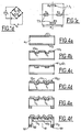
- a matrix of biosensors according to the invention is represented at figure 1a . It has a two-dimensional network of biosensors each of which is composed of a membrane 2 and a plurality of piezoresistive or piezoelectric sensitive elements. As shown more particularly in figure 1b , the sensitive elements referenced 3 1 , 3 2 , 3 3 and 3 4 are arranged to allow detection when connected WHEATSTONE bridge.
- Each of the membranes 2 is delimited between the plane main face referenced 4 of the substrate 1 and the bottom 9 of the open cavity at its upper part (in its use configuration which is inverted with respect to that shown to illustrate the method of manufacture), which is carried out in the substrate (see figure 2e ).
- the gauges R1 to R4 having the same resistance are located in the middle of each edge of a square (or rectangular) membrane of side a, so that the gauges are in the zones of maximum stress and the responses of the gauges are in identical absolute value.
- the variations of the resistances R2 and R4 on the one hand and R1 and R3 on the other hand have opposite signs, whence the electrical assembly of the Wheatstone bridge to the figure 1d . This configuration minimizes the thermodynamic stresses generated by the interconnections for the membrane.
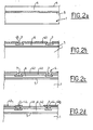
- a manufacturing process for the implementation of piezoresistive sensitive elements will now be described in connection with the Figures 2a to 2f from a starting substrate 1 which has a buried layer 5 made of SiO 2 surmounted by a surface layer 6 whose thickness is a few microns (for an SOI type substrate), and which may be less than one micron for a SIMOX type substrate.
- a layer of oxide 41 is deposited on the surface of the substrate in which openings 45 are made which will make it possible to produce the piezoresistances.
- a first (optional) implantation of germanium is firstly performed to pre-amalgamate locally the surface layer 6.
- boron B or BF 2 is implanted at a density of 10 14 per cm 2 (for example to produce the zones 7 constituting the piezoresistances).
- a rapid thermal annealing lasting from a few seconds to a few seconds between 900 and 1100 ° C, this rapid treatment being optionally followed by a conventional annealing at a lower temperature, for example for 20 minutes at 800 ° C., the combination of these treatments making it possible to electrically activate the implanted boron (or BF 2) atoms and reduce the defects created during implantation ionic.
- the substrate is then passivated ( Figure 2c ) by depositing an oxide layer 42, for example a plasma chemical vapor-type cold deposition ("PECVD” or "LPCVD”).
- PECVD plasma chemical vapor-type cold deposition
- An aluminum metallization is then carried out to form electrical conductors 43 1 and 43 2 to take the contacts 44 on the piezoresistive sensitive elements 7 ( figure 2d ).
- open cavities 8 are made by deep dry ionic etching after masking by a thick resin layer 11.
- TMAH ammonium hydroxide tetramethyl
- KOH potassium hydroxide tetramethyl
- EDP ethylene diamine pyrocatechol
- the interfacial silicon oxide layer 5 of the substrate 1 serves as a stop layer for etching.
- This layer 5 is then optionally removed by RIE dry etching on the rear face, which is recommended rather than the use a chemical solution of fluoridic acid that may damage the front of the device.
- Each open cavity or dish 8 then has a thin membrane 40 incorporating piezoresistances 3 1 to 3 4 or R 1 to R 4 (corresponding to zones 44).
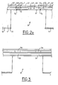
- a variant of the process is shown in relation to the Figures 4a to 4f .
- the implantation of B or BF 2 is carried out through openings 45 1 to produce the piezoresistances 7 1 ( figure 4b ).
- This implantation is followed by implantation annealing and thermal oxidation to isolate the resistors (41 1 , 42 1 , figure 4c ).
- Apertures are then made in the oxide layer 41 1 , 42 1 to make the contacts 44 1 by metallization Al, then the contacts are etched and the Al is annealed so as to obtain the metallizations (43 11 , 43 22 ) ( figure 4d ).
- a resin layer 1, which is insulated, is then opened to open the backside 41 2 oxide ( figure 4e ).
- a deep dry etching is performed on the rear face to form the open cavities 81 and the membranes 40 1 ( figure 4f ).
- the cavities 81 square or rectangular
- the steps of this method are carried out in the same way as for the process of the Figures 2a to 2c except that the substrate is Si without buried oxide layer.
- the proposed configuration adapts to any robotized system of depositing samples for depositing drops whose volume does not exceed a few nanoliters.
- contact deposition systems using microneedles or using piezoelectric systems are suitable.
- the biosensor matrix makes it possible to design an integrated detection system based on the fine measurement of mass variation resulting from hybridization or interaction between biological molecules by means of a piezoresistive or piezoelectric system disposed on a membrane (or on a beam).
- This device makes it possible to obtain from a qualitative point of view the detection of interactions between biological molecules, and from a quantitative point of view a measure of the quantity of molecules that have interacted, as well as a follow-up of the kinetics of reaction. this without resorting to steps of marking the biological molecules using radioactive or fluorescent markers.
- micro and nanotechnology allows mass and low cost production of the biosensor matrix. Given the principle of measuring mass variation, the molecules do not require prior labeling.
- the use of these sensors allows rapid and quantitative detection as well as real-time monitoring of the kinetics of the intermolecular reaction.
- the reduction in size of the resonant devices that makes it possible to obtain the technique used makes it possible to obtain a high resonance frequency, typically several MHz, with a high quality factor leading to an increase in sensitivity.
- the low mass of the active part of the microdevices makes them all the more sensitive to the slightest mass variation following the pairing of a complementary species.
- the measurements can be carried out in vacuum, and in this case washing and drying steps are used after hybridization. They can also be performed in a liquid medium, and in this case, the drying step is not performed.
- the biosensor matrix comprises a large number of resonant structures, it is possible to perform statistical analysis of the data if the same deposition is performed on each structure or to work simultaneously with several types of deposition.
- the invention can also be implemented by performing, by a method known per se, piezoelectric sensitive elements 54 arranged at localized locations on the main surface of the substrate (see FIG. figure 3 ).
- the open cavities 8 are then made as indicated above, to form deformable structures 40 (membrane, or beam embedded at one or two ends).
Landscapes
- Chemical & Material Sciences (AREA)
- Analytical Chemistry (AREA)
- Health & Medical Sciences (AREA)
- Physics & Mathematics (AREA)
- General Health & Medical Sciences (AREA)
- Pathology (AREA)
- Engineering & Computer Science (AREA)
- Life Sciences & Earth Sciences (AREA)
- General Physics & Mathematics (AREA)
- Immunology (AREA)
- Acoustics & Sound (AREA)
- Hematology (AREA)
- Clinical Laboratory Science (AREA)
- Chemical Kinetics & Catalysis (AREA)
- Biochemistry (AREA)
- Computer Hardware Design (AREA)
- Microelectronics & Electronic Packaging (AREA)
- Micromachines (AREA)
- Pressure Sensors (AREA)
- Investigating Or Analysing Biological Materials (AREA)
- Apparatus Associated With Microorganisms And Enzymes (AREA)
- Photometry And Measurement Of Optical Pulse Characteristics (AREA)
- Measuring Or Testing Involving Enzymes Or Micro-Organisms (AREA)
Description
- La présente invention concerne une matrice de biocapteurs utilisant l'effet piézorésistif ou bien l'effet piézoélectrique pour la détection d'interaction moléculaire spécifique. Elle concerne également son procédé de fabrication.
- Il a déjà été proposé, par exemple dans les brevets des Etats-Unis
US-5,719,324 etUS-6,054,277 de mettre en oeuvre un biocapteur intégré sur une puce semi-conductrice, le biocapteur comprenant un ou plusieurs leviers encastrés à une extrémité. - L'évolution de la technique impose de réaliser un grand nombre de mesures et par conséquent de disposer d'un grand nombre de biocapteurs. Or, les techniques connues ne permettent de réaliser que des biocapteurs individuels, ce qui conduit à des coûts de fabrication élevés qu'il est hautement souhaitable de réduire.
- A cet effet, l'invention propose une technique permettant d'intégrer sur un même substrat semi-conducteur un grand nombre de biocapteurs.
- L'invention concerne ainsi une Matrice de biocapteurs apte à la détection d'interactions spécifiques d'oligonucléotides (ADN/ADN ; ADN/ARN) ou de protéines (ADN/protéines) ou d'antigènes anticorps et comprenant un substrat en matériau semiconducteur, caractérisée en ce qu'elle présente une surface principale plane (4) ainsi que des cavités ouvertes (8), ménagées à partir d'une surface plane (10) opposée à ladite surface plane (4), et dont chacune présente une structure déformable (40, 50) présentant une pluralité d'éléments sensibles qui sont des piézorésistances (44) ou des éléments piézoélectriques (54) disposés entre le fond (9, 91) desdites cavités (8) et la surface plane (4), et qui sont montés en pont de Wheatstone.
- Ces cavités sont ainsi des cavités ouvertes qui débouchent sur la surface opposée à la surface principale plane.
- Selon un mode de réalisation préféré, au moins une structure déformable est une membrane.
- Alternativement, une structure déformable peut comporter au moins une poutre encastrée à une ou de préférence à deux extrémités, par exemple par mise en oeuvre d'une attaque superficielle localisée.
- Le substrat peut être en silicium, et préférentiellement être d'un type présentant une couche enterrée en SiO2 (substrat SOI).
- Selon une première variante, au moins une structure déformable intègre au moins un élément sensible piézorésistif.
- Selon une deuxième variante, au moins une structure déformable présente au moins un élément sensible piézoélectrique déposé sur le substrat.
- Afin de permettre un raccordement électrique, notamment par multiplexage des éléments sensibles, la surface plane présente avantageusement des métallisations.
- L'invention concerne également un procédé de fabrication d'une matrice de biocapteurs du type précité, caractérisé en ce qu'il met en oeuvre :
- a) la réalisation de dits éléments sensibles en des premiers endroits localisés de la surface principale plane du substrat,
- b) la réalisation de dites cavités à partir de deuxième(s) endroits localisés d'une deuxième surface du substrat qui est opposée à la surface principale, pour obtenir des structures déformables comportant au moins un dit élément sensible.
- Le procédé peut être caractérisé en ce que lesdits éléments sensibles sont piézorésistifs, en ce que le substrat est en silicium et comporte éventuellement une couche enterrée en silice (SiO2), surmontée d'une couche superficielle monocristaline, en ce que a comporte :
- a1) le dépôt d'une couche de masquage sur une première surface du substrat, par exemple sur la couche superficielle monocristalline,
- a2) la réalisation d'ouvertures en des premiers endroits localisés de la couche de masquage,
- a3) l'implantation d'ions en vue de la réalisation desdits éléments sensibles piézorésistifs,
- b1) le dépôt d'une couche de masquage sur une deuxième surface du substrat opposée à ladite première surface,
- b2) la réalisation d'ouvertures dans les deuxièmes endroits localisés de la couche de masquage,
- b3) la réalisation par attaque chimique desdites cavités. Dans le cas d'un substrat pourvu d'une couche enterrée de SiO2 l'attaque peut être poursuivie jusqu'à la couche de SiO2 qui forme une couche d'arrêt, cette couche de SiO2 pouvant être conservée ou bien ultérieurement partiellement enlevée, par exemple pour former une couche de passivation
- Alternativement, cette couche de SiO2 peut être entièrement enlevée.
- Avantageusement, l'étape a3 met en oeuvre
- a31) une implantation d'ions contenant du bore par exemple du fluorure de bore ;
- a32) un recuit thermique.
- L'étape a31 est préférentiellement précédée d'une préamorphisation de la surface du substrat auxdits premiers endroits localisés de la couche de masquage, par exemple par implantation de germanium.
- Avantageusement, le procédé met en oeuvre la réalisation d'électrodes de prise de contact électrique pour les éléments sensibles piézorésistifs.
- Selon une autre variante, les éléments sensibles sont piézoélectriques et l'étape a comporte le dépôt sur lesdits premiers endroits localisés d'une couche piézoélectrique suivi d'un recuit de cristallisation.
- Le procédé met avantageusement en oeuvre la réalisation d'électrodes de prise de contact électrique pour les éléments sensibles piézoélectriques.
- D'autres caractéristiques et avantages de l'invention apparaîtront mieux à la lecture de la description qui va suivre donnée à titre d'exemple non limitatif, en liaison avec les dessins dans lesquels :
- les
figures 1a, et 1b illustrent un exemple de réalisation d'une matrice selon l'invention, lafigure 1b étant un agrandi d'un détail de lafigure 1a ; lafigure 1c illustre un mode de réalisation préférée et lafigure 1d illustre le, montage en pont de Wheatstone ; - les
figures 2a à 2e illustrent le procédé de fabrication d'une matrice présentant des éléments sensibles piézorésistifs ; et - la
figure 3 illustre un procédé de réalisation de l'invention dans lesquels les éléments sensibles sont piézoélectriques ; - les
figures 4 à 4f illustrent un autre procédé de fabrication à partir d'un substrat en Si, notamment monocristallin. - L'invention concerne le domaine de la génomique, de la protéomique (puces à ADN, puces à protéines) et plus généralement les biopuces. Elle concerne un dispositif permettant la détection d'interactions spécifiques, d'oligonucléotides (ADN/ADN ; ADN/ARN) ou de protéines (ADN/protéines) ou d'antigènes-anticorps.
- Un tel système permet de s'affranchir des techniques de marquage des sondes et donc des systèmes de détection externes par fluorescence ou radioactivité.
- Le principe de détection proposé peut être comparé à celui des microbalances à cristal de quartz dans lesquels une variation de la masse induit une variation de la fréquence de résonance et/ou de l'amortissement de la structure en résonance.
- Toutefois, la mise en oeuvre dans le cadre de l'invention d'éléments sensibles de faible épaisseur de type piézoélectrique ou préférentiellement piézorésistif permet d'améliorer les performances et notamment la sensibilité par rapport aux microbalances à cristal de quartz, pour lesquels le facteur de qualité Q doit être très élevé pour que la sensibilité soit suffisante.
- Dans le cadre de l'invention, les variations de masse à détecter sont consécutives à l'appariement d'ADN cibles (ou d'ARN, de protéines ou tout type d'interaction entre molécules) avec les sondes d'ADN présentes sur l'élément sensible.
- La technique selon l'invention permet de mettre en oeuvre sur un même substrat une multitude de structures résonantes indépendantes de dimensions réduites, par exemple quelques microns, et non plus un seul dispositif comme c'est le cas dans l'art antérieur. Cette approche est possible, car les techniques d'élaboration de piézorésistances ultraminces ou de couches piézoélectriques ultraminces sont compatibles avec des technologies silicium, ce qui permet de fabriquer des microstructures résonantes de manière collective et à faible coût.
- D'autre part, la réduction des dimensions de ces microstructures, permet de réduire leur masse. Ainsi, plus la masse des structures résonantes est faible, plus l'ajout d'une masse modifie la réponse de ladite structure, et on augmente ainsi la sensibilité du système.
- Dans le cadre de la présente invention, on utilise préférentiellement les éléments sensibles piézorésistifs, en particulier des membranes. Ceci présente deux avantages :
- 1/ En mode statique, lors de la phase d'élaboration de la puce à ADN durant laquelle le matériel biologique est déposé par contact sur les microdispositifs piézorésistifs grâce à un système de dépôt automatisé, les membranes déformables permettent de contrôler très précisément la force d'appui ainsi que la durée durant laquelle cette force est appliquée, ce qui assure un contrôle de la quantité de solution déposée sur le microdispositif. Ce type de contrôle n'est pas possible avec des structures de type poutre encastrée à une extrémité qui sont utilisées dans certains cas pour la détection d'interactions, par exemple une poutre telle que décrite dans le brevet
US-5,807,758 . - Le système proposé permet de plus, en statique lors de la phase de dépôt, si on utilise des systèmes de dépôt par contact, de connaître la force et le temps d'appui des aiguilles sur les dispositifs où s'effectuent les dépôts. Si on utilise un système de dépôt sans contact (système microfluidique avec éjection de gouttes), le système selon l'invention permet de connaître la quantité de liquide déposé, la masse de la goutte induisant une variation de la contrainte et donc une variation de la piézorésistance (ou un effet piézoélectrique).
- Il s'agit d'un point important, car il est ainsi possible d'identifier un défaut d'alignement entre les différentes aiguilles utilisées pour réaliser un dépôt collectif, une usure éventuelle des aiguilles ou bien encore les disparités concernant les temps de contact des différentes pointes, ou bien encore les disparités dans la taille des gouttes, qui existent très souvent dans le cas de systèmes à éjection de gouttes.
- Cette possibilité de détection est importante car elle conditionne la qualité des dépôts (volume et donc concentration déposée, et la fiabilité des résultats).
- Ce système est compatible avec un contrôle actif du dépôt avec boucle de contre-réaction permettant de corriger les erreurs en fonction de la force et du temps de contact lors du dépôt.
- Alternativement, le procédé peut être utilisé pour calibrer les systèmes de dépôt par contact par réglage de la hauteur des pointes, vérification de l'usure et des effets de dérive mécanique du système ou bien encore les effets d'interaction parasites comme les vibrations, ou bien pour calibrer les systèmes de dépôt sans contact pour régler la fréquence d'éjection des gouttes ou bien encore la distance entre la zone d'éjection et la surface du microdispositif.
- Un tel dispositif de calibration peut être utilisé avant ou après une série de dépôts dans le cas d'un système avec contact, et après dépôt dans le cas d'un système sans contact.
- 2/ En mode dynamique, lors de la phase de détection, les membranes permettent d'assurer un découplage mécanique efficace entre les différents monodispositifs résonants.
- Ceci permet d'éviter de possibles interactions parasites via le substrat entre les différents modes de résonance de chaque microdispositif. Un tel phénomène est susceptible d'apparaître si les microdispositifs sont disposés à même le substrat de départ.
- Ce mode dynamique peut être également utilisé pour la phase de dépôt de la même manière que décrit précédemment sous le point 1/ pour contrôler la qualité des dépôts.
- Le procédé de fabrication sera précisé ci-après.
- D'un point de vue technologique, il s'agit de fabriquer des membranes (ou des poutres) de dimensions les plus réduites' possibles, ce qui suppose de réduire en conséquence l'épaisseur des piézorésistances. A cet effet, l'invention met en oeuvre une préamorphisation localisée du substrat suivie d'une implantation de bore ou de fluorure de bore notamment à très faible énergie, par exemple 15keV, associée à un recuit thermique rapide. Par exemple un recuit pendant 1 à 10 secondes entre 900 et 1100°C permettent d'obtenir les résultats recherchés.
- On obtient ainsi des jonctions p+/n ultraminces qui présentent un caractère piézorésistif.
- Dans le cadre de l'application envisagée, les membranes (avantageusement de forme carrée ou rectangulaire, et éventuellement circulaire) sont par exemple en silicium monocristallin, d'épaisseur uniforme (quelques microns à quelques centaines de microns) d'orientation (100) et ont des bords parallèles aux directions <110>. Le substrat est par exemple de type n dosé à 1017 atomes/cm3. Les piézorésistances (ou jauges piézorésistives) dont la valeur nominale est de l'ordre de 1 kΩ à 10 kΩ (typiquement quelques kΩ par exemple entre 4 et 4,5 kΩ) sont implantées pour leur conférer un dopage, notamment P+, compris entre 1018 et 1019 atomes/cm3. La longueur de ces jauges est compris entre 50 microns et quelques centaines de microns (par exemple 50 µ et 500 µ) et leur largeur est comprise entre 10 microns et quelques dizaines de microns (par exemple entre 10 µ et 50 µ, voire 100 µ). L'épaisseur h de la membrane est par exemple comprise entre 2 et 30 µ et est par exemple égale à 15 µ. La membrane est par exemple carrée de côté a = 500 µm. Un montage en pont de Wheatstone permet de compenser la dérive thermique de la résistance en rejetant le mode commun. Une diminution de la dimension des jauges permet d'optimiser la contrainte moyenne vue par la jauge et donc la sensibilité. Cette diminution doit être en rapport avec les tolérances du procédé de fabrication mis en oeuvre, afin de ne pas augmenter indûment la dispersion des valeurs des jauges.
- La force appliquée F peut être approximée par la formule suivante (R = R1 = R2 = R3 = R4)
pour une membrane carrée en Si monocristallin de côté a et de hauteur h
- ν = 0,26 (coefficient de Poisson)
- on obtient pour h = 15 µ, a = 500 µm et Va = 10V
- F1 = 4,05 m N pour ΔVs1 = 0,534 volt
- F2 = 2,60 m N pour ΔVs2 = 0,343 volt
- et pour une membrane circulaire en silicium monocristallin de hauteur h :

- avec π44 = 138,1 e-11 (en Pa-1)

- Va = tension appliquée au pont de Wheatstone
- ΔVs = différence de tension aux bornes du pont de Wheatstone (voir
figure 1d ). - Application : h = 15 µ, a = 500 µm, et Va = 10 V,
- En pratique, on pourra étalonner le capteur en relevant les variation de tension recueillies aux bornes de pont de Wheatstone lorsqu'on applique à la membrane des forces calibrées.
- La technique décrite présente l'avantage de conduire à des capteurs piézorésistifs en forme de poutre qui présentent une sensibilité très nettement améliorée par rapport à celles obtenues par les techniques classiques d'implantation de bore qui conduisent à des valeurs de profondeur de jonction' plus importantes.. Cette amélioration vient du fait que la combinaison des deux techniques précitées (préamorphisation et implantation) associées à des techniques de recuit thermique rapide permet de parfaitement confiner la zone piézorésistive à la surface du dispositif où la contrainte mécanique est maximale lors de la déflection, que ce soit en mode statique ou dynamique.
- L'intérêt de la technique de l'invention est d'obtenir des piézorésistances ayant une profondeur de jonction très faible notamment entre 50 nm et 200 nm, ou bien entre 50 nm et 100 nm et, par exemple égale à 70 nm, avec un substrat de départ classique en Si par exemple dopé à 1017 par cm3, dans lequel le bore est implanté avec une énergie de 15keV. Par comparaison, une implantation de bore suivi d'un recuit classique peut donner des profondeurs de jonction de 0,3 à 0,4µm.
- Cette technique d'élaboration de piézorésistrance ultramince, combinant une préamorphisation une implantation de bore ou de BF2 à basse énergie associée à un recuit thermique rapide peut être utilisé pour la fabrication aussi bien de membranes intégrant des capteurs piézorésistifs que de leviers piézorésistifs dans le cadre de la présente invention (parfaitement adaptée également à la microscopie à force atomique).
- On notera cependant qu'il est nettement plus intéressant dans le cadre de l'application envisagée d'obtenir une membrane continue, ce qui fait que la face plane du substrat reste étanche et que celui-ci peut être utilisé comme une lame de verre classique, sans qu'il y ait besoin de procéder à des opérations de nettoyage particulières entre deux utilisations successives de la biopuce.
- L'invention sera décrite ci-après pour l'obtention d'une matrice de biocapteurs comprenant des membranes par exemple d'épaisseur 5 microns intégrant quatre piézorésistances montées en pont de WHEATSTONE. Sur chaque dispositif peut être disposé un plot d'or, par exemple de 200 microns de diamètre, isolé de manière appropriée des prises de contact électriques, qui permet de localiser les interactions moléculaires (interaction chimique sur l'or avec une chimie de greffage spécifique pour l'or).
- Les résonances mécaniques à vide (mode fondamental) des microdispositifs peuvent être mesurés électriquement via les variations des piézorésistances. Un protocole d'étalonnage permet d'effectuer la mesure de la variation de fréquence de résonance consécutivement à l'appariement de brins d'ADN complémentaires, à l'interaction antigène anticorps, ADN/protéines, etc...
- Une matrice de biocapteurs selon l'invention est représentée à la
figure 1a . Elle présente un réseau à deux dimensions de biocapteurs dont chacun est composé d'une membrane 2 et d'une pluralité d'éléments sensibles piézorésistifs ou piézoélectriques. Comme le montre plus particulièrement lafigure 1b , les éléments sensibles référencés 31, 32, 33 et 34 sont disposés de manière à permettre une détection lorsqu'ils sont connectés en pont de WHEATSTONE. Chacune des membranes 2 est délimitée entre la face principale plane référencée 4 du substrat 1 et le fond 9 de la cavité ouverte à sa partie supérieure (dans sa configuration d'utilisation qui est inversée par rapport à celle qui est représentée pour illustrer le procédé de fabrication), qui est réalisée dans le substrat (voir lafigure 2e ). Dans le mode préféré qui est représenté à lafigure 1c , les jauges R1 à R4 ayant la même résistance sont situées au milieu de chaque bord d'une membrane carrée (ou rectangulaire) de côté a, de sorte que les jauges se trouvent dans les zones de contrainte maximale et les réponses des jauges sont en valeur absolue identiques. Les variations des résistances R2 et R4 d'une part et R1 et R3 d'autre part ont des signes opposés, d'où le montage électrique du pont de Wheastone à lafigure 1d . Cette configuration minimise les contraintes thermodynamiques engendrées par les interconnexions pour la membrane. - Un procédé de fabrication pour la mise en oeuvre d'éléments sensibles piézorésistifs sera maintenant décrit en liaison avec les
figures 2a à 2f , à partir d'un substrat de départ 1 qui présente une couche enterrée 5 en SiO2 surmontée d'une couche superficielle 6 dont l'épaisseur est de quelques microns (pour un substrat de type SOI), et qui peut être inférieure à un micron pour un substrat de type SIMOX. - A la
figure 2b , on dépose à la surface du substrat une couche d'oxyde 41 dans laquelle on ménage des ouvertures 45 qui vont permettre de réaliser les piézorésistances. On réalise tout d'abord une première implantation (optionnelle) de germanium pour préamorphiser localement la couche superficielle 6. Ensuite, on implante du bore B ou du BF2 à une densité de 1014 par cm2 (par exemple pour réaliser les zones 7 constituant les piézorésistances). On réalise ensuite, par exemple à l'aide d'une lampe halogène, un recuit thermique rapide (RTA) d'une durée de quelques secondes à quelques dizaine de secondes entre 900 et 1100°C, ce traitement rapide étant éventuellement suivi d'un recuit classique à plus basse température, par exemple pendant 20 minutes à 800°C, l'association de ces traitements permettant d'activer électriquement les atomes de bores (ou de BF2) implantés et de réduire les défauts créés lors de l'implantation ionique. - Le substrat est ensuite passivé (
figure 2c ) par dépôt d'une couche d'oxyde 42, par exemple un dépôt à froid de type chimique en phase vapeur sous plasma ("PECVD" ou "LPCVD"). Une métallisation d'aluminium est ensuite réalisée pour former des conducteurs électriques 431 et 432 pour prendre les contacts 44 sur les éléments sensibles piézorésistifs 7 (figure 2d ). - Ensuite, comme représenté à la
figure 2e , on réalise à partir de la face arrière 10 du substrat 1 des cavités ouvertes 8 par gravure ionique sèche profonde après masquage par une couche de résine épaisse 11. - On peut également réaliser une gravure humide de type TMAH (hydroxyde d'ammonium tétraméthyl), KOH ou EDP (éthylène diamine pyrocatechol), mais dans ce cas une couche de nitrure 11 est utilisée comme couche de masquage.
- Dans l'un et l'autre cas, la couche d'oxyde de silicium interfaciale 5 du substrat 1 sert de couche d'arrêt à la gravure.
- Cette couche 5 est ensuite éventuellement enlevée par gravure sèche RIE en face arrière, qui est préconisée plutôt que l'utilisation d'une solution chimique d'acide fluoridrique qui peut endommager la face avant du dispositif.
- Chaque cavité ouverte ou cuvette 8 présente alors une membrane mince 40 intégrant des piézorésistànces 31 à 34 ou R1 à R4 (correspondant aux zones 44).
- Une variante du procédé est représentée en relation avec les
figures 4a à 4f . On part d'un substrat Si qui est soumis sur ses deux faces à une oxydation (double oxydation 411, 412,figure 4a ). Ensuite on réalise, éventuellement après préamorphisation, l'implantation de B ou de BF2 à travers des ouvertures 451 pour réaliser les piézorésistances 71 (figure 4b ). Cette implantation est suivie d'un recuit d'implantation et d'une oxydation thermique pour isoler les résistances (411, 421,figure 4c ). On réalise ensuite des ouvertures dans la couche d'oxyde 411, 421 pour réaliser les contacts 441 par métallisation Al, puis on effectue la gravure des contacts et un recuit de l'Al de manière à obtenir les métallisations (4311, 4322) (figure 4d ). On dispose une couche de résine 101 qui est isolée pour ouvrir ensuite l'oxyde de 412 en face arrière (figure 4e ). Enfin, on réalise une gravure sèche profonde en face arrière pour former les cavités ouvertes 81 et les membranes 401 (figure 4f ). Les cavités 81 (carrées ou rectangulaires) sont délimitées par un fond 91 et quatre bords latéraux 82. D'une manière générale, les étapes de ce procédé sont réalisées de la même façon que pour le procédé desfigures 2a à 2c , sauf que le substrat est en Si sans couche d'oxyde enterré. - La configuration proposée s'adapte à n'importe quel système robotisé de dépôt d'échantillons permettant de déposer des gouttes dont le volume n'excède pas quelques nanolitres. A titre d'exemple, des systèmes à dépôt par contact à l'aide de microaiguilles ou à l'aide de systèmes piézoélectriques conviennent.
- La matrice de biocapteurs permet de concevoir un système de détection intégré reposant sur la mesure fine de variation de masse consécutive à une hybridation ou à une interaction entre molécules biologiques à l'aide d'un système piézorésistif ou piézoélectrique disposé sur une membrane (ou sur une poutre).
- Ce dispositif permet d'obtenir d'un point de vue qualitatif la détection d'interactions entre molécules biologiques, et d'un point de vue quantitatif une mesure de la quantité de molécules ayant interagi, ainsi qu'un suivi de la cinétique de réaction, ceci sans avoir recours à des étapes de marquage des molécules biologiques à l'aide de marqueurs radioactifs ou fluorescents.
- L'utilisation de micro et nanotechnologie permet la production en masse et à faible coût de la matrice de biocapteurs. Compte-tenu du principe de mesure de variation de masse, les molécules ne nécessitent pas de marquage préalable. L'utilisation de ces capteurs permet une détection rapide et quantitative ainsi qu'un suivi en temps réel de la cinétique de la réaction intermoléculaire.
- La réduction de taille des dispositifs résonants que permet d'obtenir la technique mise en oeuvre, autorise l'obtention d'une fréquence de résonance élevée, typiquement de plusieurs MHz, avec un facteur de qualité élevé conduisant à une augmentation de la sensibilité. De plus, la faible masse de la partie active des microdispositifs les rend d'autant plus sensibles à la moindre variation de masse consécutive à l'appariement d'une espèce complémentaire.
- Les mesures peuvent être effectuées dans le vide, et dans ce cas on a recours à des étapes de lavage et de séchage après hybridation. Elles peuvent être également réalisées en milieu liquide, et dans ce cas, l'étape de séchage n'est pas effectuée.
- Dans le vide, on privilégie la mesure de variation de résonance ou d'impédance, et dans le liquide la mesure de l'amortissement visqueux.
- Du fait que la matrice de biocapteurs comprend un grand nombre de structures résonantes, il est possible d'effectuer une analyse statistique des données si le même dépôt est effectué sur chaque structure ou de travailler simultanément avec plusieurs types de dépôt.
- Les principaux avantages de la matrice de biocapteurs selon l'invention sont donc :
- 1) un faible coût de fabrication grâce à l'utilisation d'une technique de fabrication collective (micro et nanotechnologies),
- 2) la possibilité de fabriquer de manière collective des structures résonantes, en réseau, de très petites dimensions, pour augmenter la sensibilité et la densité d'intégration,
- 3) la possibilité de travailler sur de faibles volumes utiles, ce qui réduit le temps nécessaire à l'analyse ainsi que le coût de fabrication de la puce,
- 4) la possibilité de suivre in situ la cinétique des réactions qui rentrent en jeu,
- 5) la possibilité de détecter des réactions d'hybridations sans avoir recours à des techniques de marquage de type fluorescence ou de radioactivité,
- 6) la possibilité d'une réutilisation des structures par simple lavage ou par chauffage à température compatible avec la déshybridation (entre 50 et 60°C),
- 7) une automatisation de la lecture et un rendu de résultats ultra rapide.
- L'invention peut également être mise en oeuvre en réalisant par un procédé connu en soi des éléments sensibles piézoélectriques 54 disposés en des endroits localisés de la surface principale du substrat (voir la
figure 3 ). Les cavités ouvertes 8 sont ensuite réalisées comme indiqué précédemment, pour constituer des structures déformables 40 (membrane, ou poutre encastrée à une ou deux extrémités).
Claims (17)
- Matrice de biocapteurs apte à la détection d'interactions spécifiques d'oligonucléotides (ADN/ADN; ADN/ARN) ou de protéines (ADN/protéines) ou d' antigènes anticorps et comprenant un substrat en matériau semiconducteur, caractérisée en ce qu'elle présente une surface principale plane (4) ainsi que des cavités ouvertes (8), ménagées à partir d'une surface plane (10) opposée à ladite surface plane (4), et dont chacune présente une structure déformable (40, 50) présentant une pluralité d'éléments sensibles qui sont des piézorésistances (44) ou des éléments piézoélectriques (54) disposés entre le fond (9, 91) desdites cavités (8) et la surface plane (4), et qui sont montés en pont de Wheatstone.
- Matrice selon la revendication 1, caractérisée en ce qu'au moins une structure déformable est une membrane (40, 50).
- Matrice selon une des revendications 1 ou 2, caractérisée en ce qu'au moins une structure déformable comporte au moins une poutre.
- Matrice selon la revendication 2 caractérisée en ce que les piézorésistances ont la même résistance et sont situées au milieu de chaque bord d'une membrane carrée ou rectangulaire.
- Matrice selon une des revendications précédentes, caractérisé en ce que le substrat est en silicium.
- Matrice selon la revendication 5, caractérisée en ce que le substrat présente une couche enterrée (5) en SiO2.
- Matrice selon une des revendications précédentes, caractérisée en ce que la surface principale plane (4) présente des métallisations (431, 432) permettant le raccordement électrique desdits éléments sensibles (44, 54).
- Procédé de fabrication d'une matrice de biocapteurs selon une des revendications précédentes, caractérisé en ce qu'il met en oeuvre :a) la réalisation de dits éléments sensibles (44, 54) en des premiers endroits localisés de la surface principale plane du substrat,b) la réalisation de dites cavités (8) à partir de deuxième(s) endroits localisés d'une deuxième surface (10) du substrat qui est opposée à la surface principale plane (4), pour obtenir des structures déformables (40, 50) comportant au moins un dit élément sensible (44, 54).
- Procédé selon la revendication 8, caractérisé en ce que lesdits éléments sensibles (44) sont piézorésistifs, en ce que le substrat est en silicium et a comporte :a1) le dépôt d'une couche de masquage (41) sur une première surface du substrat,a2) la réalisation d'ouvertures (45) en des premiers endroits localisés de la couche de masquage (41),a3) l'implantation d'ions en vue de la réalisation desdits éléments sensibles piézorésistifs (44),et en ce que b comporte :b1) le dépôt d'une couche de masquage (11) sur la deuxième surface (10) du substrat, opposée à la première surface,b2) la réalisation d'ouvertures dans les deuxièmes endroits localisés de la couche de masquage (11),b3) la réalisation par attaque chimique desdites cavités (8).
- Procédé selon la revendication 9, caractérisé en ce que le substrat comporte une couche enterrée (5) en silice surmontée d'une couche superficielle monocristalline (6) et en ce que a1 comporte le dépôt de ladite couche de masquage (41) sur la surface de la couche superficielle monocristalline (6) qui constitue ladite première surface du substrat et en ce qu'en b3, l'attaque est poursuivie au moins jusqu'à la couche enterrée en silice (5) qui forme une couche d'arrêt.
- Procédé selon une des revendications 9 ou 10, caractérisé en ce que a3 met en oeuvrea31) une implantation de bore ou de BF2a32) un recuit thermique
- Procédé selon la revendication 11, caractérisé en ce que a31 est précédé d'une préamorphisation de la surface du substrat auxdits premiers endroits localisés de la couche de masquage.
- Procédé selon la revendication 12, caractérisé en ce que ladite préamorphisation est réalisée par implantation de Ge.
- Procédé selon une des revendications 9 à 13, caractérisé en ce qu'il met en oeuvre la réalisation d'électrodes (431, 432) de prise de contact électrique pour les éléments sensibles piézorésistifs (44).
- Procédé selon la revendication 8, caractérisé en ce que les éléments sensibles sont piézoélectriques et en ce que a comporte : le dépôt sur lesdits premiers endroits localisés d'une couche piézoélectrique (54) suivi d'un recuit de cristallisation.
- Procédé selon la revendication 15, caractérisé en ce qu'il met en oeuvre la réalisation d'électrodes de prise de contact électrique pour les éléments sensibles piézoélectriques.
- Procédé d'utilisation d'une matrice de biocapteurs selon une des revendications 1 à 8, caractérisé en ce qu'il met en oeuvre :a) une étape préliminaire de contrôle, à l'aide desdits éléments sensibles, de la force d'appui exercée par un dispositif de dépose d'échantillon, sur chacun des biocapteurs et/ou de la durée durant laquelle une force d'appui est appliquée par ledit dispositif de dépose d'échantillons,b) une étape dynamique de détection au cours de laquelle on mesure les variations de masse des échantillons déposés sur chacun des biocapteurs.
Applications Claiming Priority (3)
| Application Number | Priority Date | Filing Date | Title |
|---|---|---|---|
| FR0105545A FR2823998B1 (fr) | 2001-04-25 | 2001-04-25 | Matrice de biocapteurs et son procede de fabrication |
| FR0105545 | 2001-04-25 | ||
| PCT/FR2002/001419 WO2002086479A1 (fr) | 2001-04-25 | 2002-04-25 | Matrice de biocapteurs et son procede de fabrication |
Publications (2)
| Publication Number | Publication Date |
|---|---|
| EP1381852A1 EP1381852A1 (fr) | 2004-01-21 |
| EP1381852B1 true EP1381852B1 (fr) | 2011-06-22 |
Family
ID=8862659
Family Applications (1)
| Application Number | Title | Priority Date | Filing Date |
|---|---|---|---|
| EP02730368A Expired - Lifetime EP1381852B1 (fr) | 2001-04-25 | 2002-04-25 | Matrice de biocapteurs et son procede de fabrication |
Country Status (7)
| Country | Link |
|---|---|
| US (1) | US6930365B2 (fr) |
| EP (1) | EP1381852B1 (fr) |
| JP (1) | JP4196025B2 (fr) |
| AT (1) | ATE514074T1 (fr) |
| CA (1) | CA2445285C (fr) |
| FR (1) | FR2823998B1 (fr) |
| WO (1) | WO2002086479A1 (fr) |
Families Citing this family (8)
| Publication number | Priority date | Publication date | Assignee | Title |
|---|---|---|---|---|
| DE102004019357A1 (de) * | 2004-04-21 | 2005-11-17 | Infineon Technologies Ag | Verfahren zur Funktionalisierung von Biosensor-Chips |
| JP4987385B2 (ja) * | 2005-09-07 | 2012-07-25 | 財団法人神奈川科学技術アカデミー | パターン化された有機薄膜とその製造方法 |
| IT1392576B1 (it) * | 2008-12-30 | 2012-03-09 | St Microelectronics Rousset | Dispositivo di rilevamento elettronico di materiali biologici e relativo processo di fabbricazione |
| US9476026B2 (en) * | 2009-03-12 | 2016-10-25 | New Jersey Institute Of Technology | Method of tissue repair using a piezoelectric scaffold |
| WO2011148774A1 (fr) * | 2010-05-24 | 2011-12-01 | 独立行政法人物質・材料研究機構 | Capteur de contrainte superficielle |
| CN108027291B (zh) * | 2015-09-30 | 2020-04-24 | 日立汽车系统株式会社 | 力学量测量装置和使用它的压力传感器 |
| KR102649456B1 (ko) | 2016-10-31 | 2024-03-19 | 미코노스 리미티드 | 생체 세포 주입을 위한 니들 매니퓰레이터들의 어레이 |
| WO2020252213A1 (fr) * | 2019-06-13 | 2020-12-17 | Mekonos Inc. | Structures à système micro-électro-mécanique et leurs applications |
Citations (2)
| Publication number | Priority date | Publication date | Assignee | Title |
|---|---|---|---|---|
| US5189914A (en) * | 1988-02-29 | 1993-03-02 | The Regents Of The University Of California | Plate-mode ultrasonic sensor |
| US5212988A (en) * | 1988-02-29 | 1993-05-25 | The Reagents Of The University Of California | Plate-mode ultrasonic structure including a gel |
Family Cites Families (10)
| Publication number | Priority date | Publication date | Assignee | Title |
|---|---|---|---|---|
| US5252294A (en) * | 1988-06-01 | 1993-10-12 | Messerschmitt-Bolkow-Blohm Gmbh | Micromechanical structure |
| US5184515A (en) * | 1989-06-22 | 1993-02-09 | Ic Sensors, Inc. | Single diaphragm transducer with multiple sensing elements |
| DE4309207C2 (de) * | 1993-03-22 | 1996-07-11 | Texas Instruments Deutschland | Halbleitervorrichtung mit einem piezoresistiven Drucksensor |
| EP0706646B1 (fr) * | 1993-07-02 | 1998-03-25 | Institut Für Molekulare Biologie E.V. | Porte-echantillons et son utilisation |
| US6329139B1 (en) * | 1995-04-25 | 2001-12-11 | Discovery Partners International | Automated sorting system for matrices with memory |
| US5719324A (en) * | 1995-06-16 | 1998-02-17 | Lockheed Martin Energy Systems, Inc. | Microcantilever sensor |
| US6054277A (en) * | 1996-05-08 | 2000-04-25 | Regents Of The University Of Minnesota | Integrated microchip genetic testing system |
| DE60023917T2 (de) * | 1999-05-03 | 2006-07-27 | Nanonord A/S | Sensor für ein mikrofluidisches bearbeitungssystem |
| ITVA20000042A1 (it) * | 2000-12-15 | 2002-06-15 | St Microelectronics Srl | Sensore di pressione monoliticamente integrato e relativo processo direalizzazione. |
| DE10114036A1 (de) * | 2001-03-22 | 2002-10-02 | Bosch Gmbh Robert | Verfahren zur Herstellung von mikromechanischen Sensoren und damit hergestellte Sensoren |
-
2001
- 2001-04-25 FR FR0105545A patent/FR2823998B1/fr not_active Expired - Fee Related
-
2002
- 2002-04-25 AT AT02730368T patent/ATE514074T1/de not_active IP Right Cessation
- 2002-04-25 JP JP2002583959A patent/JP4196025B2/ja not_active Expired - Lifetime
- 2002-04-25 US US10/475,324 patent/US6930365B2/en not_active Expired - Fee Related
- 2002-04-25 CA CA002445285A patent/CA2445285C/fr not_active Expired - Fee Related
- 2002-04-25 WO PCT/FR2002/001419 patent/WO2002086479A1/fr active Application Filing
- 2002-04-25 EP EP02730368A patent/EP1381852B1/fr not_active Expired - Lifetime
Patent Citations (2)
| Publication number | Priority date | Publication date | Assignee | Title |
|---|---|---|---|---|
| US5189914A (en) * | 1988-02-29 | 1993-03-02 | The Regents Of The University Of California | Plate-mode ultrasonic sensor |
| US5212988A (en) * | 1988-02-29 | 1993-05-25 | The Reagents Of The University Of California | Plate-mode ultrasonic structure including a gel |
Also Published As
| Publication number | Publication date |
|---|---|
| JP4196025B2 (ja) | 2008-12-17 |
| CA2445285C (fr) | 2009-12-22 |
| WO2002086479A1 (fr) | 2002-10-31 |
| FR2823998A1 (fr) | 2002-10-31 |
| ATE514074T1 (de) | 2011-07-15 |
| JP2004531720A (ja) | 2004-10-14 |
| EP1381852A1 (fr) | 2004-01-21 |
| CA2445285A1 (fr) | 2002-10-31 |
| US20040185592A1 (en) | 2004-09-23 |
| FR2823998B1 (fr) | 2004-01-02 |
| US6930365B2 (en) | 2005-08-16 |
Similar Documents
| Publication | Publication Date | Title |
|---|---|---|
| US7552645B2 (en) | Detection of resonator motion using piezoresistive signal downmixing | |
| US6933164B2 (en) | Method of fabrication of a micro-channel based integrated sensor for chemical and biological materials | |
| EP0766060B1 (fr) | Procédé de fabrication de pièces de micromécanique ayant une partie en diamant constituée au moins d'une pointe. | |
| EP0950185A1 (fr) | Microsystemes pour analyses biologiques, leur utilisation pour la detection d'analytes et leur procede de realisation | |
| EP1381852B1 (fr) | Matrice de biocapteurs et son procede de fabrication | |
| EP2866000B1 (fr) | Dispositif optomécanique d'actionnement et/ou de détection du déplacement d'un élément mécanique, notamment pour la détection gravimétrique | |
| FR2964651A1 (fr) | Dispositif a poutre suspendue et moyens de detection piezoresistive du deplacement de celle-ci, et procede de fabrication du dispositif | |
| US20020102743A1 (en) | Apparatus and method for visually identifying micro-forces with a palette of cantilever array blocks | |
| EP2233919A1 (fr) | Micro-dispositif de détection in situ de particules d'intérêt dans un milieu fluide, et procédé de mise en oeuvre | |
| EP3059300A1 (fr) | Dispositif de manipulation de cellules biologiques au moyen d'un support vibrant | |
| US8122761B2 (en) | Biosensor based on polymer cantilevers | |
| EP2343543A1 (fr) | Capteur biologique à mesure électrochimique et/ou électrique et à électrode de diamant et circuit électronique intégrés | |
| EP2866020B1 (fr) | Dispositif de détection électromécanique, pour la détection gravimétrique | |
| US6794296B1 (en) | Aperture in a semiconductor material, and the production and use thereof | |
| CN101903285B (zh) | 在基片上组装元件的方法 | |
| US20060073502A1 (en) | Apparatus for detecting bio-bonding and method thereof | |
| FR2887986A1 (fr) | Procede de caracterisation d'un objet deformable et capteur pour la mise en oeuvre d'un tel procede | |
| EP2189787B1 (fr) | Procédé de réalisation d'une puce de détection d'éléments biologiques | |
| FR2916271A1 (fr) | Circuit electronique permettant la mesure de masse de materiau biologique et procede de fabrication | |
| WO2020149739A1 (fr) | Dispositif à semi-conducteur monolithique pour détection optique | |
| FR3106005A1 (fr) | Capteur de concentration d’especes en milieu liquide offrant une resolution augmentee | |
| Tsouti et al. | Design and fabrication of a Si micromechanical capacitive array for DNA sensing | |
| KR100450261B1 (ko) | 고감도 초소형 캔틸레버 센서 및 그 제조방법 | |
| EP4155717B1 (fr) | Dispositif et procédé de détection d'espèces chimiques ou biologiques | |
| WO2009141516A1 (fr) | Dispositif pour la detection gravimetrique de particules en milieu fluide, comprenant un oscillateur traverse par une veine fluidique, procede de realisation et methode de mise en oeuvre du dispositif. |
Legal Events
| Date | Code | Title | Description |
|---|---|---|---|
| PUAI | Public reference made under article 153(3) epc to a published international application that has entered the european phase |
Free format text: ORIGINAL CODE: 0009012 |
|
| 17P | Request for examination filed |
Effective date: 20031016 |
|
| AK | Designated contracting states |
Kind code of ref document: A1 Designated state(s): AT BE CH CY DE DK ES FI FR GB GR IE IT LI LU MC NL PT SE TR |
|
| AX | Request for extension of the european patent |
Extension state: AL LT LV MK RO SI |
|
| 17Q | First examination report despatched |
Effective date: 20100428 |
|
| GRAP | Despatch of communication of intention to grant a patent |
Free format text: ORIGINAL CODE: EPIDOSNIGR1 |
|
| RIN1 | Information on inventor provided before grant (corrected) |
Inventor name: COCHETEAU, EMELINE Inventor name: NICU, LIVIU Inventor name: MARTINEZ, AUGUSTIN Inventor name: BERGAUD, CHRISTIAN Inventor name: BELIER, BENOIT,RESIDENCE D'ILOT DES COURS |
|
| GRAS | Grant fee paid |
Free format text: ORIGINAL CODE: EPIDOSNIGR3 |
|
| GRAA | (expected) grant |
Free format text: ORIGINAL CODE: 0009210 |
|
| AK | Designated contracting states |
Kind code of ref document: B1 Designated state(s): AT BE CH CY DE DK ES FI FR GB GR IE IT LI LU MC NL PT SE TR |
|
| REG | Reference to a national code |
Ref country code: GB Ref legal event code: FG4D Free format text: NOT ENGLISH |
|
| REG | Reference to a national code |
Ref country code: CH Ref legal event code: EP |
|
| REG | Reference to a national code |
Ref country code: IE Ref legal event code: FG4D Free format text: LANGUAGE OF EP DOCUMENT: FRENCH |
|
| REG | Reference to a national code |
Ref country code: DE Ref legal event code: R096 Ref document number: 60240338 Country of ref document: DE Effective date: 20110804 |
|
| REG | Reference to a national code |
Ref country code: NL Ref legal event code: VDEP Effective date: 20110622 |
|
| PG25 | Lapsed in a contracting state [announced via postgrant information from national office to epo] |
Ref country code: SE Free format text: LAPSE BECAUSE OF FAILURE TO SUBMIT A TRANSLATION OF THE DESCRIPTION OR TO PAY THE FEE WITHIN THE PRESCRIBED TIME-LIMIT Effective date: 20110622 |
|
| PG25 | Lapsed in a contracting state [announced via postgrant information from national office to epo] |
Ref country code: CY Free format text: LAPSE BECAUSE OF FAILURE TO SUBMIT A TRANSLATION OF THE DESCRIPTION OR TO PAY THE FEE WITHIN THE PRESCRIBED TIME-LIMIT Effective date: 20110622 Ref country code: AT Free format text: LAPSE BECAUSE OF FAILURE TO SUBMIT A TRANSLATION OF THE DESCRIPTION OR TO PAY THE FEE WITHIN THE PRESCRIBED TIME-LIMIT Effective date: 20110622 Ref country code: FI Free format text: LAPSE BECAUSE OF FAILURE TO SUBMIT A TRANSLATION OF THE DESCRIPTION OR TO PAY THE FEE WITHIN THE PRESCRIBED TIME-LIMIT Effective date: 20110622 Ref country code: GR Free format text: LAPSE BECAUSE OF FAILURE TO SUBMIT A TRANSLATION OF THE DESCRIPTION OR TO PAY THE FEE WITHIN THE PRESCRIBED TIME-LIMIT Effective date: 20110923 |
|
| PG25 | Lapsed in a contracting state [announced via postgrant information from national office to epo] |
Ref country code: NL Free format text: LAPSE BECAUSE OF FAILURE TO SUBMIT A TRANSLATION OF THE DESCRIPTION OR TO PAY THE FEE WITHIN THE PRESCRIBED TIME-LIMIT Effective date: 20110622 |
|
| REG | Reference to a national code |
Ref country code: IE Ref legal event code: FD4D |
|
| PG25 | Lapsed in a contracting state [announced via postgrant information from national office to epo] |
Ref country code: IE Free format text: LAPSE BECAUSE OF FAILURE TO SUBMIT A TRANSLATION OF THE DESCRIPTION OR TO PAY THE FEE WITHIN THE PRESCRIBED TIME-LIMIT Effective date: 20110622 Ref country code: PT Free format text: LAPSE BECAUSE OF FAILURE TO SUBMIT A TRANSLATION OF THE DESCRIPTION OR TO PAY THE FEE WITHIN THE PRESCRIBED TIME-LIMIT Effective date: 20111024 |
|
| PLBE | No opposition filed within time limit |
Free format text: ORIGINAL CODE: 0009261 |
|
| STAA | Information on the status of an ep patent application or granted ep patent |
Free format text: STATUS: NO OPPOSITION FILED WITHIN TIME LIMIT |
|
| 26N | No opposition filed |
Effective date: 20120323 |
|
| PG25 | Lapsed in a contracting state [announced via postgrant information from national office to epo] |
Ref country code: IT Free format text: LAPSE BECAUSE OF FAILURE TO SUBMIT A TRANSLATION OF THE DESCRIPTION OR TO PAY THE FEE WITHIN THE PRESCRIBED TIME-LIMIT Effective date: 20110622 |
|
| PG25 | Lapsed in a contracting state [announced via postgrant information from national office to epo] |
Ref country code: DK Free format text: LAPSE BECAUSE OF FAILURE TO SUBMIT A TRANSLATION OF THE DESCRIPTION OR TO PAY THE FEE WITHIN THE PRESCRIBED TIME-LIMIT Effective date: 20110622 |
|
| REG | Reference to a national code |
Ref country code: DE Ref legal event code: R097 Ref document number: 60240338 Country of ref document: DE Effective date: 20120323 |
|
| BERE | Be: lapsed |
Owner name: CENTRE NATIONAL DE LA RECHERCHE SCIENTIFIQUE Effective date: 20120430 |
|
| PG25 | Lapsed in a contracting state [announced via postgrant information from national office to epo] |
Ref country code: MC Free format text: LAPSE BECAUSE OF NON-PAYMENT OF DUE FEES Effective date: 20120430 |
|
| REG | Reference to a national code |
Ref country code: CH Ref legal event code: PL |
|
| GBPC | Gb: european patent ceased through non-payment of renewal fee |
Effective date: 20120425 |
|
| REG | Reference to a national code |
Ref country code: FR Ref legal event code: ST Effective date: 20121228 |
|
| PG25 | Lapsed in a contracting state [announced via postgrant information from national office to epo] |
Ref country code: CH Free format text: LAPSE BECAUSE OF NON-PAYMENT OF DUE FEES Effective date: 20120430 Ref country code: GB Free format text: LAPSE BECAUSE OF NON-PAYMENT OF DUE FEES Effective date: 20120425 Ref country code: BE Free format text: LAPSE BECAUSE OF NON-PAYMENT OF DUE FEES Effective date: 20120430 Ref country code: LI Free format text: LAPSE BECAUSE OF NON-PAYMENT OF DUE FEES Effective date: 20120430 |
|
| REG | Reference to a national code |
Ref country code: DE Ref legal event code: R119 Ref document number: 60240338 Country of ref document: DE Effective date: 20121101 |
|
| PG25 | Lapsed in a contracting state [announced via postgrant information from national office to epo] |
Ref country code: FR Free format text: LAPSE BECAUSE OF NON-PAYMENT OF DUE FEES Effective date: 20120430 |
|
| PG25 | Lapsed in a contracting state [announced via postgrant information from national office to epo] |
Ref country code: ES Free format text: LAPSE BECAUSE OF FAILURE TO SUBMIT A TRANSLATION OF THE DESCRIPTION OR TO PAY THE FEE WITHIN THE PRESCRIBED TIME-LIMIT Effective date: 20111003 |
|
| PG25 | Lapsed in a contracting state [announced via postgrant information from national office to epo] |
Ref country code: TR Free format text: LAPSE BECAUSE OF FAILURE TO SUBMIT A TRANSLATION OF THE DESCRIPTION OR TO PAY THE FEE WITHIN THE PRESCRIBED TIME-LIMIT Effective date: 20110622 |
|
| PG25 | Lapsed in a contracting state [announced via postgrant information from national office to epo] |
Ref country code: LU Free format text: LAPSE BECAUSE OF NON-PAYMENT OF DUE FEES Effective date: 20120425 |
|
| PG25 | Lapsed in a contracting state [announced via postgrant information from national office to epo] |
Ref country code: DE Free format text: LAPSE BECAUSE OF FAILURE TO SUBMIT A TRANSLATION OF THE DESCRIPTION OR TO PAY THE FEE WITHIN THE PRESCRIBED TIME-LIMIT Effective date: 20121101 |