EP1381087A2 - Solid-state image pick-up device - Google Patents
Solid-state image pick-up device Download PDFInfo
- Publication number
- EP1381087A2 EP1381087A2 EP03254343A EP03254343A EP1381087A2 EP 1381087 A2 EP1381087 A2 EP 1381087A2 EP 03254343 A EP03254343 A EP 03254343A EP 03254343 A EP03254343 A EP 03254343A EP 1381087 A2 EP1381087 A2 EP 1381087A2
- Authority
- EP
- European Patent Office
- Prior art keywords
- solid
- state image
- image pick
- vertical transfer
- channel stopper
- Prior art date
- Legal status (The legal status is an assumption and is not a legal conclusion. Google has not performed a legal analysis and makes no representation as to the accuracy of the status listed.)
- Withdrawn
Links
- 239000000126 substance Substances 0.000 claims abstract description 12
- 229910021420 polycrystalline silicon Inorganic materials 0.000 claims description 19
- 239000000758 substrate Substances 0.000 claims description 11
- 238000009792 diffusion process Methods 0.000 claims description 10
- 239000012535 impurity Substances 0.000 claims description 10
- 239000004065 semiconductor Substances 0.000 claims description 8
- 230000000694 effects Effects 0.000 description 13
- 238000002955 isolation Methods 0.000 description 9
- 239000000203 mixture Substances 0.000 description 6
- XUIMIQQOPSSXEZ-UHFFFAOYSA-N Silicon Chemical compound [Si] XUIMIQQOPSSXEZ-UHFFFAOYSA-N 0.000 description 3
- 230000007547 defect Effects 0.000 description 3
- 229910052710 silicon Inorganic materials 0.000 description 3
- 239000010703 silicon Substances 0.000 description 3
- 238000009825 accumulation Methods 0.000 description 2
- 239000013078 crystal Substances 0.000 description 2
- 230000003247 decreasing effect Effects 0.000 description 1
- 230000006866 deterioration Effects 0.000 description 1
- 230000002542 deteriorative effect Effects 0.000 description 1
- 238000010586 diagram Methods 0.000 description 1
- 229910001385 heavy metal Inorganic materials 0.000 description 1
- 238000004519 manufacturing process Methods 0.000 description 1
- 230000001590 oxidative effect Effects 0.000 description 1
- 230000002265 prevention Effects 0.000 description 1
- 238000004088 simulation Methods 0.000 description 1
- 238000009751 slip forming Methods 0.000 description 1
- 238000010408 sweeping Methods 0.000 description 1
Images






Classifications
-
- H—ELECTRICITY
- H10—SEMICONDUCTOR DEVICES; ELECTRIC SOLID-STATE DEVICES NOT OTHERWISE PROVIDED FOR
- H10F—INORGANIC SEMICONDUCTOR DEVICES SENSITIVE TO INFRARED RADIATION, LIGHT, ELECTROMAGNETIC RADIATION OF SHORTER WAVELENGTH OR CORPUSCULAR RADIATION
- H10F39/00—Integrated devices, or assemblies of multiple devices, comprising at least one element covered by group H10F30/00, e.g. radiation detectors comprising photodiode arrays
- H10F39/10—Integrated devices
- H10F39/12—Image sensors
- H10F39/15—Charge-coupled device [CCD] image sensors
- H10F39/158—Charge-coupled device [CCD] image sensors having arrangements for blooming suppression
-
- H—ELECTRICITY
- H10—SEMICONDUCTOR DEVICES; ELECTRIC SOLID-STATE DEVICES NOT OTHERWISE PROVIDED FOR
- H10F—INORGANIC SEMICONDUCTOR DEVICES SENSITIVE TO INFRARED RADIATION, LIGHT, ELECTROMAGNETIC RADIATION OF SHORTER WAVELENGTH OR CORPUSCULAR RADIATION
- H10F39/00—Integrated devices, or assemblies of multiple devices, comprising at least one element covered by group H10F30/00, e.g. radiation detectors comprising photodiode arrays
- H10F39/10—Integrated devices
- H10F39/12—Image sensors
- H10F39/15—Charge-coupled device [CCD] image sensors
- H10F39/153—Two-dimensional or three-dimensional array CCD image sensors
-
- H—ELECTRICITY
- H10—SEMICONDUCTOR DEVICES; ELECTRIC SOLID-STATE DEVICES NOT OTHERWISE PROVIDED FOR
- H10F—INORGANIC SEMICONDUCTOR DEVICES SENSITIVE TO INFRARED RADIATION, LIGHT, ELECTROMAGNETIC RADIATION OF SHORTER WAVELENGTH OR CORPUSCULAR RADIATION
- H10F39/00—Integrated devices, or assemblies of multiple devices, comprising at least one element covered by group H10F30/00, e.g. radiation detectors comprising photodiode arrays
- H10F39/80—Constructional details of image sensors
-
- H—ELECTRICITY
- H10—SEMICONDUCTOR DEVICES; ELECTRIC SOLID-STATE DEVICES NOT OTHERWISE PROVIDED FOR
- H10F—INORGANIC SEMICONDUCTOR DEVICES SENSITIVE TO INFRARED RADIATION, LIGHT, ELECTROMAGNETIC RADIATION OF SHORTER WAVELENGTH OR CORPUSCULAR RADIATION
- H10F39/00—Integrated devices, or assemblies of multiple devices, comprising at least one element covered by group H10F30/00, e.g. radiation detectors comprising photodiode arrays
- H10F39/80—Constructional details of image sensors
- H10F39/807—Pixel isolation structures
Definitions
- the present invention relates to a solid-state image pick-up device such as a CCD, and more particularly to a solid-state image pick-up device including a channel stopper having a trench structure for isolating adjacent elements.
- Fig. 10 is a sectional view showing the main part of a conventional solid-state image pick-up device.
- a vertical transfer path (VCCD) 1 in an n region is formed in the surface portion of the semiconductor substrate of the solid-state image pick-up device, and an isolation is carried out between the adjacent vertical transfer paths 1 through a channel stopper (CS) 2 constituted by a p-type impurity layer.
- CS channel stopper
- a transfer and read electrode 3 comprising a polycrystalline silicon is provided on the surface of the semiconductor substrate.
- the p-type impurity of the channel stopper 2 is diffused to the adjacent vertical transfer path 1 so that the effective transfer path (channel) width of the vertical transfer path 1 is decreased, resulting in a reduction in the channel potential of the vertical transfer path 1.
- This influence becomes more remarkable in manufacture in which the width of the vertical transfer path 1 is more reduced, which is referred to as a narrow channel effect.
- Fig. 11 is a graph showing the narrow channel effect.
- a potential of 5.8V is applied in a vertical transfer path in which a channel stopper (CS) is not provided. If the channel stopper is provided on either side, a potential of 5.3V is applied. If the channel stopper is provided on both sides, a potential of 4.6V is applied. Consequently, a charge is insufficiently read from a photodiode (pixel) to the vertical transfer path 1 or is insufficiently transferred along the vertical transfer path 1.
- CS channel stopper
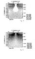
- Fig. 12 is a chart in which a potential gradient around the channel stopper 2 shown in Fig. 10 is simulated, and the channel stopper 2 is formed around a position of 0.75 ⁇ m on an X coordinate.
- Fig. 12 is a chart showing a two-dimensional potential gradient obtained when a voltage of 0V is applied to the electrode 3 in Fig. 10
- Fig. 13 is a chart showing a two-dimensional potential gradient obtained when a voltage of -8V is applied to the electrode 3.
- Figs. 14 and 15 are charts showing a two-dimensional potential gradient and a one-dimensional potential which are obtained when a read voltage of +16V is applied to the electrode 3
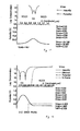
- Fig. 16 is a chart showing a one-dimensional potential obtained when a charge is stored in the vertical transfer path.
- Fig. 17 is a view showing the structure of a conventional solid-state image pick-up device (for example, JP-A-2002-57381) in which an oxide film 4 is buried in the channel stopper 2as compared with the solid-state image pick-up device shown in Fig. 10.
- Figs. 18, 19 and 20 are views in which two-dimensional potential gradients obtained by application of voltages of 0V, -8V (transfer voltage) and +16V (read voltage) to the electrode 3 of the solid-state image pick-up device are simulated.
- Fig. 21 is a chart showing a one-dimensional potential obtained when +16V is applied to the electrode 3
- Fig. 22 is a chart showing a one-dimensional potential obtained when a charge is stored in the vertical transfer path.
- the channel stopper 2 is formed to have a depth of 0.4 ⁇ m around a position of 0.75 ⁇ m on the X coordinate.
- the interface 5 is depleted. Therefore, there is also a problem in that the generation of a dark current from a dangling bond and the generation of a white scratch from a high-speed GR center (a heavy metal atom) are increased remarkably.
- a solid-state image pick-up device comprises, on a semiconductor substrate, a plurality of light receiving sensor sections, a vertical transfer path formed close to each of the light receiving sensor sections, and a channel stopper provided between the adjacent vertical transfer paths and formed by an insulating layer having a trench structure, wherein a conductive substance to which a predetermined voltage is applied is buried in the insulating layer.
- a negative voltage should be applied as the predetermined voltage to bring an interface into a hole accumulation state when a signal charge is an electron
- a positive voltage shouldbe applied as the predetermined voltage to bring the interface into an electron accumulation state when the signal charge is a hole.
- the predetermined voltage should be a pulse having an opposite phase to that of a read pulse to be applied to a transfer electrode of the vertical transfer path.
- a diffusion region having an opposite conductivity type to that of the light receiving sensor section should be formed in a lowermost part of the channel stopper.
- the conductive substance should also be doped with a doped impurity in the diffusion region, and the conductive substance and the diffusion region should be thus set in a connecting state.
- the conductive substance should be a polycrystalline silicon.
- FIG. 1 is a plan view showing the main part of a solid-state image pick-up device according to a first embodiment of the invention.
- a solid-state image pick-up device 10 is of a so-called honeycomb type in which a pixel 11 comprising a photodiode is formed with a shift of a 1/2 pitch every other line in a horizontal direction.
- Each pixel 11 has a vertical transfer path 12 formed zigzag at both sides thereof, and a channel stopper 13 is provided on the right side of each vertical transfer path 12. Consequently, the vertical transfer path 12 is isolated from an adjacent element in portions other than a necessary region 14 for reading a charge from the pixel 11. While the embodiment is intended for the solid-state image pick-up device of the honeycomb type, the invention can also be applied to a solid-state image pick-up device of a Bayer type having a channel stopper.
- Fig. 2 is a sectional view taken along a line II - II in Fig. 1.
- the vertical transfer path 12 doped with an n-type impurity is provided in the surface portion of a semiconductor (silicon in this example) substrate of the solid-state image pick-up device 10, and the channel stopper 13 is provided between the adjacent vertical transfer paths 12.
- the channel stopper 13 is manufactured by providing a trench having a depth of 0.4 ⁇ m between the vertical transfer paths 12, oxidizing the surface of the semiconductor substrate to form the oxide film 14 and burying a polycrystalline silicon 15 in the trench.
- a transfer and read electrode 17 comprising a polycrystalline silicon is formed on the surface of the vertical transfer path 12 through a surface oxide film 16.
- the polycrystalline silicon 15 buried in the channel stopper 13 is continuously formed over the full length of the vertical transfer path 12 along the vertical transfer path 12.
- a predetermined voltage is applied to a connecting pad provided on the semiconductor substrate which is not shown
- the polycrystalline silicon 15 is set to have a predetermined voltage over a full length after a predetermined time in accordance with a time constant determined by the resistance value of the polycrystalline silicon 15.
- a negative voltage is always applied to the polycrystalline silicon 15.
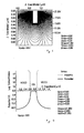
- Fig. 3 is a chart in which a potential gradient around the channel stopper 13 shown in Fig. 1 is simulated.
- the channel stopper 13 is formed to have a depth of 0.4 ⁇ m around a position of 0.75 ⁇ m on an X coordinate and 0V is applied to the electrode 17 and the polycrystalline silicon 15.
- Fig. 4 is a chart showing a two-dimensional potential gradient in which -8V is applied to the electrode 17
- Figs. 5 and 6 are charts showing a two-dimensional potential gradient and a one-dimensional potential which are obtained when a read voltage of +16V is applied to the electrode 17 respectively.
- Fig. 7 is a chart showing a one-dimensional potential obtained when a charge is stored in the vertical transfer path.
- the channel stopper 13 As is apparent from Figs. 3, 4, 5 and 6, a potential difference between the transfer path 12 and the channel stopper 13 is great and a potential is also low in the deep portion of the channel stopper 13. Therefore, the channel stopper 13 according to the embodiment produces a high isolation effect. Consequently, a charge mixture with the adjacent vertical transfer path can be prevented in charge reading, and furthermore, the charge trap into the interface 5 described with reference to Fig. 17 can also be prevented. Furthermore, there is no p-type impurity. Consequently, the narrow channel effect can also be relieved.
- the same voltage is set to be negative so that the potential difference between the channel stopper 13 and the transfer path 12 is further increased and the charge mixture between the transfer paths 12 can be prevented still more.
- the polycrystalline silicon 15 having an almost equal coefficient of thermal expansion to that of the silicon substrate of the solid-state image pick-up device 10 is buried in the channel stopper 13 having a trench structure. Therefore, a stress received from the silicon substrate by the polycrystalline silicon 15 becomes very small so that the generation of a crystal defect due to the stress can be reduced.
- the potential of the interface 5 described with reference to Fig. 17 is shifted to be negative so that the charge (electron) can further be prevented from being trapped into the interface 5.
- the start timing of the offset pulse is caused to slightly precede the start timing of a read potential pulse.
- the degree of precedence is calculated from a time constant determined by the resistance value of the polycrystalline silicon 15 described above.
- Fig. 9 is a sectional view showing the main part of a solid-state image pick-up device according to a second embodiment of the invention.
- the embodiment is different from the first embodiment in that a diffusion layer 18 is provided in the lower position of a channel stopper 13.
- the diffusion layer 18 is formed by diffusing an impurity having an opposite conductivity type to that of a pixel (a light receiving sensor section) 11, that is, a p-type impurity in an example shown in the drawing. Consequently, an isolation region reaches the deep portion of a substrate so that the mixture of a signal charge between the pixels 11 can be prevented still more.
- the channel stopper 13 can be utilized as a path for sweeping a charge having an opposite polarity to that of the signal charge. It is suitable that a polycrystalline silicon 15 in the channel stopper 13 should also be dopedwith the p-type impurity having a high concentration to connect the polycrystalline silicon 15 to the p-type diffusion layer 18. Thus, the charge can be swept smoothly.
- a conductive substance is buried in a channel stopper and the potential of the conducive substance is controlled to have a predetermined potential. Consequently, the isolation effect of the channel stopper can be enhanced and the narrow channel effect of a vertical transfer path can be relieved so that the generation of an image defect, a reduction in a transfer efficiency and an increase in a dark current can be prevented.
Landscapes
- Solid State Image Pick-Up Elements (AREA)
- Transforming Light Signals Into Electric Signals (AREA)
Abstract
Description
- The present invention relates to a solid-state image pick-up device such as a CCD, and more particularly to a solid-state image pick-up device including a channel stopper having a trench structure for isolating adjacent elements.
- Fig. 10 is a sectional view showing the main part of a conventional solid-state image pick-up device. A vertical transfer path (VCCD) 1 in an n region is formed in the surface portion of the semiconductor substrate of the solid-state image pick-up device, and an isolation is carried out between the adjacent
vertical transfer paths 1 through a channel stopper (CS) 2 constituted by a p-type impurity layer. Moreover, a transfer and readelectrode 3 comprising a polycrystalline silicon is provided on the surface of the semiconductor substrate. - The p-type impurity of the
channel stopper 2 is diffused to the adjacentvertical transfer path 1 so that the effective transfer path (channel) width of thevertical transfer path 1 is decreased, resulting in a reduction in the channel potential of thevertical transfer path 1. This influence becomes more remarkable in manufacture in which the width of thevertical transfer path 1 is more reduced, which is referred to as a narrow channel effect. - Fig. 11 is a graph showing the narrow channel effect. For example, when the
vertical transfer path 1 has a channel width of 0.5µm, a potential of 5.8V is applied in a vertical transfer path in which a channel stopper (CS) is not provided. If the channel stopper is provided on either side, a potential of 5.3V is applied. If the channel stopper is provided on both sides, a potential of 4.6V is applied. Consequently, a charge is insufficiently read from a photodiode (pixel) to thevertical transfer path 1 or is insufficiently transferred along thevertical transfer path 1. - Fig. 12 is a chart in which a potential gradient around the
channel stopper 2 shown in Fig. 10 is simulated, and thechannel stopper 2 is formed around a position of 0.75µm on an X coordinate. Fig. 12 is a chart showing a two-dimensional potential gradient obtained when a voltage of 0V is applied to theelectrode 3 in Fig. 10, and Fig. 13 is a chart showing a two-dimensional potential gradient obtained when a voltage of -8V is applied to theelectrode 3. Moreover, Figs. 14 and 15 are charts showing a two-dimensional potential gradient and a one-dimensional potential which are obtained when a read voltage of +16V is applied to theelectrode 3, and Fig. 16 is a chart showing a one-dimensional potential obtained when a charge is stored in the vertical transfer path. - From these drawings, it is apparent that the effect of an isolation obtained by the
channel stopper 2 is small in the solid-state image pick-up device shown in Fig. 10. As shown in Figs. 14 and 15, particularly, the potential of thechannel stopper 2 also becomes deep by the influence of the potential of the transfer path, and a potential difference between thetransfer path 1 and thechannel stopper 2 is reduced and an isolation effect is small. - Fig. 17 is a view showing the structure of a conventional solid-state image pick-up device (for example, JP-A-2002-57381) in which an
oxide film 4 is buried in the channel stopper 2as compared with the solid-state image pick-up device shown in Fig. 10. Figs. 18, 19 and 20 are views in which two-dimensional potential gradients obtained by application of voltages of 0V, -8V (transfer voltage) and +16V (read voltage) to theelectrode 3 of the solid-state image pick-up device are simulated. Moreover, Fig. 21 is a chart showing a one-dimensional potential obtained when +16V is applied to theelectrode 3 and Fig. 22 is a chart showing a one-dimensional potential obtained when a charge is stored in the vertical transfer path. Thechannel stopper 2 is formed to have a depth of 0.4µm around a position of 0.75µm on the X coordinate. - In the solid-state image pick-up device shown in Fig. 17, a channel potential is 11.5V in the application of 0V and is 4.1V in the application of -8V as shown in Figs. 18 and 19 so that a degree of modulation (potential difference / voltage difference) = 0.93 is obtained. On the other hand, in the solid-state image pick-up device shown in Fig. 10, a channel potential is 10.1V in the application of 0V and is 4.2V in the application of -8V as shown in Figs. 12 and 13 so that a degree of modulation = 0.74 is obtained. More specifically, it can be guessed that an
oxide film 4 is buried in the channel stopper 2 so that the p-type impurity layer is eliminated, resulting in the prevention of a reduction in a channel potential and a relaxation in the influence of the narrow channel effect. - In the conventional solid-state image pick-up device shown in Fig. 17, however, in the case in which a charge is stored in the
vertical transfer path 1, there is a problem in that a potential difference between aninterface 5 of thechannel stopper 2 and the signal charge of thevertical transfer path 1 is reduced (see Figs. 16 and 22) and a charge (an electron in the solid-state image pick-up device shown in the drawing) is apt to be trapped into theinterface 5. When the charge is trapped into theinterface 5, the trapped charge gets into thevertical transfer path 1 of a next packet at a constant probability, thereby deteriorating a transfer efficiency. - In a recent solid-state image pick-up device mounting several million pixels, a transfer is carried out in one thousand stages or more through a one-time transfer along a vertical transfer path. For this reason, if one electron gets into an empty packet every transfer in one stage, for example, at least one thousand electrons get into the empty packet when the same packet is read from the vertical transfer path. Consequently, the picture quality of a pick-up image is considerably deteriorated.
- Furthermore, the
interface 5 is depleted. Therefore, there is also a problem in that the generation of a dark current from a dangling bond and the generation of a white scratch from a high-speed GR center (a heavy metal atom) are increased remarkably. - It is an object of the invention to provide a solid-state image pick-up device which relieves a narrow channel effect produced by a channel stopper and reduces the influence of a trapped charge and the influence of a dangling bond or a high-speed GR center.
- In order to achieve the object, a solid-state image pick-up device comprises, on a semiconductor substrate, a plurality of light receiving sensor sections, a vertical transfer path formed close to each of the light receiving sensor sections, and a channel stopper provided between the adjacent vertical transfer paths and formed by an insulating layer having a trench structure, wherein a conductive substance to which a predetermined voltage is applied is buried in the insulating layer.
- By this structure, a potential difference is made between the channel stopper (isolation region) and the vertical transfer path, and a charge mixture can be inhibited between the adjacent vertical transfer paths and a charge trap can also be prevented so that a narrow channel effect can be relieved.
- It is suitable that a negative voltage should be applied as the predetermined voltage to bring an interface into a hole accumulation state when a signal charge is an electron, and a positive voltage shouldbe applied as the predetermined voltage to bring the interface into an electron accumulation state when the signal charge is a hole. By this structure, it is possible to prevent a charge mixture, a deterioration in a transfer efficiency, an increase in a dark current and an increase in .a white scratch by a simple voltage control.
- It is suitable that the predetermined voltage should be a pulse having an opposite phase to that of a read pulse to be applied to a transfer electrode of the vertical transfer path. By this structure, a necessary voltage for a reading operation can be reduced.
- In the foregoing, it is more suitable that a diffusion region having an opposite conductivity type to that of the light receiving sensor section should be formed in a lowermost part of the channel stopper. By this structure, the isolation effect of the channel stopper can be enhanced and a signal charge mixture between pixels can be prevented still more.
- In the foregoing, it is more suitable that the conductive substance should also be doped with a doped impurity in the diffusion region, and the conductive substance and the diffusion region should be thus set in a connecting state. By this structure, it is possible to smoothly sweep a charge having an opposite polarity to that of a signal charge by utilizing the channel stopper.
- In the foregoing, it is more suitable that the conductive substance should be a polycrystalline silicon. By this structure, a difference in a coefficient of thermal expansion between the semiconductor substrate of the solid-state image pick-up device and the conductive substance is eliminated so that it is possible to reduce a crystal defect generated by a stress on the side surface of a trench.
-
- Fig. 1 is a plan view showing the main part of a solid-state image pick-up device according to a first embodiment of the invention,
- Fig. 2 is a sectional view taken along a line II - II in Fig. 1,
- Fig. 3 is a chart showing a two-dimensional potential gradient around a channel stopper which is obtained when 0V is applied to an electrode illustrated in Fig. 2,
- Fig. 4 is a chart showing a two-dimensional potential gradient around the channel stopper which is obtained when -8V is applied to the electrode illustrated in Fig. 2,
- Fig. 5 is a chart showing a two-dimensional potential gradient around the channel stopper which is obtained when +16V is applied to the electrode illustrated in Fig. 2,
- Fig. 6 is a chart showing a one-dimensional potential around the channel stopper which is obtained when +16V is applied to the electrode illustrated in Fig. 2,
- Fig. 7 is a chart showing a one-dimensional potential obtained when a charge is stored in a vertical transfer path of the solid-state image pick-up device illustrated in Fig. 2,
- Fig. 8 is a diagram showing a charge read pulse and an offset pulse,
- Fig. 9 is a sectional view showing the main part of a solid-state image pick-up device according to a second embodiment of the invention,
- Fig. 10 is a sectional view showing the main part of a conventional solid-state image pick-up device,
- Fig. 11 is a graph for explaining a narrow channel effect, channel width dependence of channel potential in vertical transfer section by presence of isolation region [applied voltage = 0V].
- Fig. 12 is a chart showing a two-dimensional potential gradient around a channel stopper which is obtained when 0V is applied to an electrode illustrated in Fig. 10,
- Fig. 13 is a chart showing a two-dimensional potential gradient around the channel stopper which is obtained when -8V is applied to the electrode illustrated in Fig. 10,
- Fig. 14 is a chart showing a two-dimensional potential gradient around the channel stopper which is obtained when +16V is applied to the electrode illustrated in Fig. 10,
- Fig. 15 is a chart showing a one-dimensional potential around the channel stopper which is obtained when +16V is applied to the electrode illustrated in Fig. 10,
- Fig. 16 is a chart showing a one-dimensional potential obtained when a charge is stored in a vertical transfer path of the solid-state image pick-up device illustrated in Fig. 10,
- Fig. 17 is a sectional view showing the main part of another conventional solid-state image pick-up device,
- Fig. 18 is a chart showing a two-dimensional potential gradient around a channel stopper which is obtained when 0V is applied to an electrode illustrated in Fig. 17,
- Fig. 19 is a chart showing a two-dimensional potential gradient around the channel stopper which is obtained when -8V is applied to the electrode illustrated in Fig. 17,
- Fig. 20 is a chart showing a two-dimensional potential gradient around the channel stopper which is obtained when +16V is applied to the electrode illustrated in Fig. 17,
- Fig. 21 is a chart showing a one-dimensional potential around the channel stopper which is obtained when +16V is applied to the electrode illustrated in Fig. 17, and
- Fig. 22 is a chart showing a one-dimensional potential obtained when a charge is stored in a vertical transfer path of the solid-state image pick-up device illustrated in Fig. 17.
-
- An embodiment of the invention will be described below with reference to the drawings.
- Fig. 1 is a plan view showing the main part of a solid-state image pick-up device according to a first embodiment of the invention. A solid-state image pick-up
device 10 is of a so-called honeycomb type in which apixel 11 comprising a photodiode is formed with a shift of a 1/2 pitch every other line in a horizontal direction. Eachpixel 11 has avertical transfer path 12 formed zigzag at both sides thereof, and achannel stopper 13 is provided on the right side of eachvertical transfer path 12. Consequently, thevertical transfer path 12 is isolated from an adjacent element in portions other than anecessary region 14 for reading a charge from thepixel 11. While the embodiment is intended for the solid-state image pick-up device of the honeycomb type, the invention can also be applied to a solid-state image pick-up device of a Bayer type having a channel stopper. - Fig. 2 is a sectional view taken along a line II - II in Fig. 1. The
vertical transfer path 12 doped with an n-type impurity is provided in the surface portion of a semiconductor (silicon in this example) substrate of the solid-state image pick-updevice 10, and thechannel stopper 13 is provided between the adjacentvertical transfer paths 12. Thechannel stopper 13 is manufactured by providing a trench having a depth of 0.4µm between thevertical transfer paths 12, oxidizing the surface of the semiconductor substrate to form theoxide film 14 and burying apolycrystalline silicon 15 in the trench. A transfer and readelectrode 17 comprising a polycrystalline silicon is formed on the surface of thevertical transfer path 12 through asurface oxide film 16. - The
polycrystalline silicon 15 buried in thechannel stopper 13 is continuously formed over the full length of thevertical transfer path 12 along thevertical transfer path 12. When a predetermined voltage is applied to a connecting pad provided on the semiconductor substrate which is not shown, thepolycrystalline silicon 15 is set to have a predetermined voltage over a full length after a predetermined time in accordance with a time constant determined by the resistance value of thepolycrystalline silicon 15. In the embodiment, a negative voltage is always applied to thepolycrystalline silicon 15. - Fig. 3 is a chart in which a potential gradient around the
channel stopper 13 shown in Fig. 1 is simulated. Thechannel stopper 13 is formed to have a depth of 0.4µm around a position of 0.75µm on an X coordinate and 0V is applied to theelectrode 17 and thepolycrystalline silicon 15. - Fig. 4 is a chart showing a two-dimensional potential gradient in which -8V is applied to the
electrode 17, and Figs. 5 and 6 are charts showing a two-dimensional potential gradient and a one-dimensional potential which are obtained when a read voltage of +16V is applied to theelectrode 17 respectively. Moreover, Fig. 7 is a chart showing a one-dimensional potential obtained when a charge is stored in the vertical transfer path. - In the case in which the charge is to be transferred through the
vertical transfer path electrode 17. When a signal charge is to be read from a pixel (a light receiving sensor section) to thevertical transfer path 12, +16V is applied to theelectrode 17. Consequently, a potential distribution around thechannel stopper 13 is brought into any of states shown in Figs. 3, 4 and 5. - As is apparent from Figs. 3, 4, 5 and 6, a potential difference between the
transfer path 12 and thechannel stopper 13 is great and a potential is also low in the deep portion of thechannel stopper 13. Therefore, thechannel stopper 13 according to the embodiment produces a high isolation effect. Consequently, a charge mixture with the adjacent vertical transfer path can be prevented in charge reading, and furthermore, the charge trap into theinterface 5 described with reference to Fig. 17 can also be prevented. Furthermore, there is no p-type impurity. Consequently, the narrow channel effect can also be relieved. - While the voltage to be applied to the
polycrystalline silicon 15 is set to be 0V in the simulation, the same voltage is set to be negative so that the potential difference between thechannel stopper 13 and thetransfer path 12 is further increased and the charge mixture between thetransfer paths 12 can be prevented still more. - In the solid-state image pick-up
device 10 according to the embodiment, moreover, thepolycrystalline silicon 15 having an almost equal coefficient of thermal expansion to that of the silicon substrate of the solid-state image pick-updevice 10 is buried in thechannel stopper 13 having a trench structure. Therefore, a stress received from the silicon substrate by thepolycrystalline silicon 15 becomes very small so that the generation of a crystal defect due to the stress can be reduced. - While the voltage to be applied to the
polycrystalline silicon 15 is always set to be negative in the embodiment, it is preferable that an offset pulse having an opposite phase should be applied to thepolycrystalline silicon 15 when a read voltage pulse of +16V is applied to theelectrode 17 as shown in Fig. 8. - Consequently, the potential of the
interface 5 described with reference to Fig. 17 is shifted to be negative so that the charge (electron) can further be prevented from being trapped into theinterface 5. The start timing of the offset pulse is caused to slightly precede the start timing of a read potential pulse. The degree of precedence is calculated from a time constant determined by the resistance value of thepolycrystalline silicon 15 described above. - Similarly, it is also possible to employ a structure in which an offset pulse having an opposite polarity to that of the transfer pulse is applied to the
polycrystalline silicon 15 in response to a transfer pulse repeating "0V" and "-8V" to be applied to theelectrode 17. - Fig. 9 is a sectional view showing the main part of a solid-state image pick-up device according to a second embodiment of the invention. The embodiment is different from the first embodiment in that a
diffusion layer 18 is provided in the lower position of achannel stopper 13. Thediffusion layer 18 is formed by diffusing an impurity having an opposite conductivity type to that of a pixel (a light receiving sensor section) 11, that is, a p-type impurity in an example shown in the drawing. Consequently, an isolation region reaches the deep portion of a substrate so that the mixture of a signal charge between thepixels 11 can be prevented still more. - Moreover, the p-
type diffusion layer 18 is provided. Consequently, thechannel stopper 13 according to the embodiment can be utilized as a path for sweeping a charge having an opposite polarity to that of the signal charge. It is suitable that apolycrystalline silicon 15 in thechannel stopper 13 should also be dopedwith the p-type impurity having a high concentration to connect thepolycrystalline silicon 15 to the p-type diffusion layer 18. Thus, the charge can be swept smoothly. - According to the invention, a conductive substance is buried in a channel stopper and the potential of the conducive substance is controlled to have a predetermined potential. Consequently, the isolation effect of the channel stopper can be enhanced and the narrow channel effect of a vertical transfer path can be relieved so that the generation of an image defect, a reduction in a transfer efficiency and an increase in a dark current can be prevented.
Claims (6)
- A solid-state image pick-up device comprising, on a semiconductor substrate, a plurality of light receiving sensor sections, a vertical transfer path formed close to each of the light receiving sensor sections, and a channel stopper provided between the adjacent vertical transfer paths and formed by an insulating layer having a trench structure, wherein a conductive substance to which a predetermined voltage is applied is buried in the insulating layer.
- The solid-state image pick-up device according to claim 1, wherein the predetermined voltage is a negative voltage if a signal charge is an electron, and is a positive voltage if the signal charge is a hole.
- The solid-state image pick-up device according to claim 1, wherein the predetermined voltage is a pulse having an opposite phase to that of a read pulse to be applied to a transfer electrode of the vertical transfer path.
- The solid-state image pick-up device according to any of claims 1 to 3, wherein a diffusion region having an opposite conductivity type to that of the light receiving sensor section is formed in a lowermost part of the channel stopper.
- The solid-state image pick-up device according to claim 4, wherein the conductive substance is also doped with a doped impurity in the diffusion region, and the conductive substance and the diffusion region are thus set in a connecting state.
- The solid-state image pick-up device according to any of claims 1 to 5, wherein the conductive substance is a polycrystalline silicon.
Applications Claiming Priority (2)
| Application Number | Priority Date | Filing Date | Title |
|---|---|---|---|
| JP2002201501 | 2002-07-10 | ||
| JP2002201501A JP4049248B2 (en) | 2002-07-10 | 2002-07-10 | Solid-state imaging device |
Publications (2)
| Publication Number | Publication Date |
|---|---|
| EP1381087A2 true EP1381087A2 (en) | 2004-01-14 |
| EP1381087A3 EP1381087A3 (en) | 2005-09-14 |
Family
ID=29728467
Family Applications (1)
| Application Number | Title | Priority Date | Filing Date |
|---|---|---|---|
| EP03254343A Withdrawn EP1381087A3 (en) | 2002-07-10 | 2003-07-09 | Solid-state image pick-up device |
Country Status (3)
| Country | Link |
|---|---|
| US (1) | US6891243B2 (en) |
| EP (1) | EP1381087A3 (en) |
| JP (1) | JP4049248B2 (en) |
Cited By (1)
| Publication number | Priority date | Publication date | Assignee | Title |
|---|---|---|---|---|
| WO2005098957A1 (en) * | 2004-04-07 | 2005-10-20 | E2V Technologies (Uk) Limited | Multiplication register for amplifying signal charge |
Families Citing this family (4)
| Publication number | Priority date | Publication date | Assignee | Title |
|---|---|---|---|---|
| JP4228887B2 (en) * | 2003-04-02 | 2009-02-25 | ソニー株式会社 | Solid-state imaging device and manufacturing method thereof |
| US7205627B2 (en) * | 2005-02-23 | 2007-04-17 | International Business Machines Corporation | Image sensor cells |
| JP4631723B2 (en) * | 2006-01-27 | 2011-02-16 | ソニー株式会社 | Solid-state imaging device |
| US8680639B1 (en) * | 2011-10-21 | 2014-03-25 | Applied Micro Circuits Corporation | Photodetector with a bandwidth-tuned cell structure |
Citations (2)
| Publication number | Priority date | Publication date | Assignee | Title |
|---|---|---|---|---|
| US5334868A (en) | 1991-02-08 | 1994-08-02 | International Business Machines Corporation | Sidewall charge-coupled device with trench isolation |
| JP2002057381A (en) | 2000-08-08 | 2002-02-22 | Res Inst Electric Magnetic Alloys | Tunnel junction film |
Family Cites Families (15)
| Publication number | Priority date | Publication date | Assignee | Title |
|---|---|---|---|---|
| JPS5875382A (en) * | 1981-07-20 | 1983-05-07 | Sony Corp | Solid-state image pickup device |
| JPH0671071B2 (en) * | 1984-09-27 | 1994-09-07 | 松下電子工業株式会社 | Solid-state image sensor |
| JPS61123172A (en) * | 1984-11-20 | 1986-06-11 | Olympus Optical Co Ltd | solid state imaging device |
| JPS61133660A (en) * | 1984-12-03 | 1986-06-20 | Olympus Optical Co Ltd | solid state image sensor |
| EP0186162B1 (en) * | 1984-12-24 | 1989-05-31 | Kabushiki Kaisha Toshiba | Solid state image sensor |
| JPH0719881B2 (en) * | 1985-05-01 | 1995-03-06 | キヤノン株式会社 | Photoelectric conversion device |
| JPS6218755A (en) * | 1985-07-18 | 1987-01-27 | Toshiba Corp | Solid-state image pickup device |
| JPS62296549A (en) * | 1986-06-17 | 1987-12-23 | Matsushita Electronics Corp | Solid-state image sensing device |
| JPH069236B2 (en) * | 1986-10-07 | 1994-02-02 | 財団法人半導体研究振興会 | Solid-state imaging device and manufacturing method thereof |
| JP3042042B2 (en) * | 1991-06-21 | 2000-05-15 | ソニー株式会社 | Solid-state imaging device |
| JP3715353B2 (en) * | 1995-09-01 | 2005-11-09 | ソニー株式会社 | Solid-state image sensor |
| JP4199387B2 (en) * | 1999-10-07 | 2008-12-17 | 富士フイルム株式会社 | Charge transfer path and solid-state imaging device using the same |
| JP2001189443A (en) * | 1999-12-28 | 2001-07-10 | Sony Corp | Solid-state imaging device and method of manufacturing the same |
| US20010054723A1 (en) * | 2000-03-17 | 2001-12-27 | Tadashi Narui | Image sensor, method of fabricating the same, and exposure apparatus, measuring device, alignment device, and aberration measuring device using the image sensor |
| JP4515617B2 (en) * | 2000-10-23 | 2010-08-04 | 富士フイルム株式会社 | Solid-state imaging device and driving method thereof |
-
2002
- 2002-07-10 JP JP2002201501A patent/JP4049248B2/en not_active Expired - Fee Related
-
2003
- 2003-07-09 EP EP03254343A patent/EP1381087A3/en not_active Withdrawn
- 2003-07-10 US US10/615,904 patent/US6891243B2/en not_active Expired - Fee Related
Patent Citations (2)
| Publication number | Priority date | Publication date | Assignee | Title |
|---|---|---|---|---|
| US5334868A (en) | 1991-02-08 | 1994-08-02 | International Business Machines Corporation | Sidewall charge-coupled device with trench isolation |
| JP2002057381A (en) | 2000-08-08 | 2002-02-22 | Res Inst Electric Magnetic Alloys | Tunnel junction film |
Cited By (1)
| Publication number | Priority date | Publication date | Assignee | Title |
|---|---|---|---|---|
| WO2005098957A1 (en) * | 2004-04-07 | 2005-10-20 | E2V Technologies (Uk) Limited | Multiplication register for amplifying signal charge |
Also Published As
| Publication number | Publication date |
|---|---|
| US6891243B2 (en) | 2005-05-10 |
| US20040007754A1 (en) | 2004-01-15 |
| EP1381087A3 (en) | 2005-09-14 |
| JP2004047630A (en) | 2004-02-12 |
| JP4049248B2 (en) | 2008-02-20 |
Similar Documents
| Publication | Publication Date | Title |
|---|---|---|
| US20130140609A1 (en) | Matrix charge-transfer image sensor with asymmetric gate | |
| US20050230720A1 (en) | Solid-state image sensor | |
| TWI521689B (en) | Multiple linear image sensor using charge integration | |
| EP0069535A2 (en) | Solid state imaging apparatus | |
| KR101064095B1 (en) | Solid-state imaging device with built-in electron multiplication | |
| EP0247503B1 (en) | Method of driving a solid state imager device | |
| US5402459A (en) | Frame transfer image sensor with electronic shutter | |
| JP3317248B2 (en) | Solid-state imaging device | |
| US6891243B2 (en) | Solid-state image pick-up device | |
| KR100193408B1 (en) | Solid-state imaging device | |
| US7052929B2 (en) | Solid state image pickup device capable of suppressing smear | |
| JP3301176B2 (en) | Charge transfer device | |
| JP3047965B2 (en) | Solid-state imaging device | |
| US7564494B2 (en) | Solid-state imaging device and its driving method for preventing damage in dynamic range | |
| JPH0661469A (en) | CCD image element | |
| JP2778673B2 (en) | Driving method of solid-state imaging device | |
| US6686963B1 (en) | Method for driving solid-state image device | |
| JPH0697416A (en) | Solid-state imaging device and manufacturing method thereof | |
| JPH0424871B2 (en) | ||
| JP3342976B2 (en) | Charge-coupled device and solid-state imaging device | |
| JPH06268923A (en) | Drive method for solid-state image pickup device | |
| JPH0424872B2 (en) | ||
| JPH02119266A (en) | Solid-state image sensing device of vertical type overflow drain structure | |
| JP2008277787A (en) | Charge transfer device | |
| JP2005243840A (en) | Charge coupled device, solid-state image pickup device, and their driving methods |
Legal Events
| Date | Code | Title | Description |
|---|---|---|---|
| PUAI | Public reference made under article 153(3) epc to a published international application that has entered the european phase |
Free format text: ORIGINAL CODE: 0009012 |
|
| AK | Designated contracting states |
Kind code of ref document: A2 Designated state(s): AT BE BG CH CY CZ DE DK EE ES FI FR GB GR HU IE IT LI LU MC NL PT RO SE SI SK TR |
|
| AX | Request for extension of the european patent |
Extension state: AL LT LV MK |
|
| PUAL | Search report despatched |
Free format text: ORIGINAL CODE: 0009013 |
|
| AK | Designated contracting states |
Kind code of ref document: A3 Designated state(s): AT BE BG CH CY CZ DE DK EE ES FI FR GB GR HU IE IT LI LU MC NL PT RO SE SI SK TR |
|
| AX | Request for extension of the european patent |
Extension state: AL LT LV MK |
|
| 17P | Request for examination filed |
Effective date: 20051124 |
|
| AKX | Designation fees paid |
Designated state(s): DE FR GB |
|
| RAP1 | Party data changed (applicant data changed or rights of an application transferred) |
Owner name: FUJIFILM CORPORATION |
|
| 17Q | First examination report despatched |
Effective date: 20090424 |
|
| STAA | Information on the status of an ep patent application or granted ep patent |
Free format text: STATUS: THE APPLICATION IS DEEMED TO BE WITHDRAWN |
|
| 18D | Application deemed to be withdrawn |
Effective date: 20120103 |