EP1380556A1 - Compound for organic el element and organic el element - Google Patents
Compound for organic el element and organic el element Download PDFInfo
- Publication number
- EP1380556A1 EP1380556A1 EP02722710A EP02722710A EP1380556A1 EP 1380556 A1 EP1380556 A1 EP 1380556A1 EP 02722710 A EP02722710 A EP 02722710A EP 02722710 A EP02722710 A EP 02722710A EP 1380556 A1 EP1380556 A1 EP 1380556A1
- Authority
- EP
- European Patent Office
- Prior art keywords
- group
- substituted
- organic
- compound
- devices
- Prior art date
- Legal status (The legal status is an assumption and is not a legal conclusion. Google has not performed a legal analysis and makes no representation as to the accuracy of the status listed.)
- Granted
Links
- 0 CC(C12)C=CC(C3=C4C(*5)=C6C5=C(*)C(*)=C5C6C3*5)=C1C4=CC=C2C(CC1)=CC=C1C1C2=C(*)CCC(C3C(*)=C4C(*)=C(*)C(C)C(*)*4C(*)C33)=C2C3=CC1 Chemical compound CC(C12)C=CC(C3=C4C(*5)=C6C5=C(*)C(*)=C5C6C3*5)=C1C4=CC=C2C(CC1)=CC=C1C1C2=C(*)CCC(C3C(*)=C4C(*)=C(*)C(C)C(*)*4C(*)C33)=C2C3=CC1 0.000 description 6
- AYCWDBOZJVBDPY-UHFFFAOYSA-N Cc(cc1)ccc1-c1c(cccc2)c2c(-c2ccccc2)c2c1cccc2 Chemical compound Cc(cc1)ccc1-c1c(cccc2)c2c(-c2ccccc2)c2c1cccc2 AYCWDBOZJVBDPY-UHFFFAOYSA-N 0.000 description 2
Images




Classifications
-
- C—CHEMISTRY; METALLURGY
- C07—ORGANIC CHEMISTRY
- C07C—ACYCLIC OR CARBOCYCLIC COMPOUNDS
- C07C13/00—Cyclic hydrocarbons containing rings other than, or in addition to, six-membered aromatic rings
- C07C13/28—Polycyclic hydrocarbons or acyclic hydrocarbon derivatives thereof
- C07C13/32—Polycyclic hydrocarbons or acyclic hydrocarbon derivatives thereof with condensed rings
- C07C13/62—Polycyclic hydrocarbons or acyclic hydrocarbon derivatives thereof with condensed rings with more than three condensed rings
-
- C—CHEMISTRY; METALLURGY
- C07—ORGANIC CHEMISTRY
- C07C—ACYCLIC OR CARBOCYCLIC COMPOUNDS
- C07C211/00—Compounds containing amino groups bound to a carbon skeleton
- C07C211/43—Compounds containing amino groups bound to a carbon skeleton having amino groups bound to carbon atoms of six-membered aromatic rings of the carbon skeleton
- C07C211/54—Compounds containing amino groups bound to a carbon skeleton having amino groups bound to carbon atoms of six-membered aromatic rings of the carbon skeleton having amino groups bound to two or three six-membered aromatic rings
-
- C—CHEMISTRY; METALLURGY
- C07—ORGANIC CHEMISTRY
- C07C—ACYCLIC OR CARBOCYCLIC COMPOUNDS
- C07C211/00—Compounds containing amino groups bound to a carbon skeleton
- C07C211/43—Compounds containing amino groups bound to a carbon skeleton having amino groups bound to carbon atoms of six-membered aromatic rings of the carbon skeleton
- C07C211/57—Compounds containing amino groups bound to a carbon skeleton having amino groups bound to carbon atoms of six-membered aromatic rings of the carbon skeleton having amino groups bound to carbon atoms of six-membered aromatic rings being part of condensed ring systems of the carbon skeleton
- C07C211/61—Compounds containing amino groups bound to a carbon skeleton having amino groups bound to carbon atoms of six-membered aromatic rings of the carbon skeleton having amino groups bound to carbon atoms of six-membered aromatic rings being part of condensed ring systems of the carbon skeleton with at least one of the condensed ring systems formed by three or more rings
-
- C—CHEMISTRY; METALLURGY
- C07—ORGANIC CHEMISTRY
- C07D—HETEROCYCLIC COMPOUNDS
- C07D213/00—Heterocyclic compounds containing six-membered rings, not condensed with other rings, with one nitrogen atom as the only ring hetero atom and three or more double bonds between ring members or between ring members and non-ring members
- C07D213/02—Heterocyclic compounds containing six-membered rings, not condensed with other rings, with one nitrogen atom as the only ring hetero atom and three or more double bonds between ring members or between ring members and non-ring members having three double bonds between ring members or between ring members and non-ring members
- C07D213/04—Heterocyclic compounds containing six-membered rings, not condensed with other rings, with one nitrogen atom as the only ring hetero atom and three or more double bonds between ring members or between ring members and non-ring members having three double bonds between ring members or between ring members and non-ring members having no bond between the ring nitrogen atom and a non-ring member or having only hydrogen or carbon atoms directly attached to the ring nitrogen atom
- C07D213/06—Heterocyclic compounds containing six-membered rings, not condensed with other rings, with one nitrogen atom as the only ring hetero atom and three or more double bonds between ring members or between ring members and non-ring members having three double bonds between ring members or between ring members and non-ring members having no bond between the ring nitrogen atom and a non-ring member or having only hydrogen or carbon atoms directly attached to the ring nitrogen atom containing only hydrogen and carbon atoms in addition to the ring nitrogen atom
- C07D213/16—Heterocyclic compounds containing six-membered rings, not condensed with other rings, with one nitrogen atom as the only ring hetero atom and three or more double bonds between ring members or between ring members and non-ring members having three double bonds between ring members or between ring members and non-ring members having no bond between the ring nitrogen atom and a non-ring member or having only hydrogen or carbon atoms directly attached to the ring nitrogen atom containing only hydrogen and carbon atoms in addition to the ring nitrogen atom containing only one pyridine ring
-
- C—CHEMISTRY; METALLURGY
- C07—ORGANIC CHEMISTRY
- C07D—HETEROCYCLIC COMPOUNDS
- C07D333/00—Heterocyclic compounds containing five-membered rings having one sulfur atom as the only ring hetero atom
- C07D333/02—Heterocyclic compounds containing five-membered rings having one sulfur atom as the only ring hetero atom not condensed with other rings
- C07D333/04—Heterocyclic compounds containing five-membered rings having one sulfur atom as the only ring hetero atom not condensed with other rings not substituted on the ring sulphur atom
- C07D333/06—Heterocyclic compounds containing five-membered rings having one sulfur atom as the only ring hetero atom not condensed with other rings not substituted on the ring sulphur atom with only hydrogen atoms, hydrocarbon or substituted hydrocarbon radicals, directly attached to the ring carbon atoms
- C07D333/08—Hydrogen atoms or radicals containing only hydrogen and carbon atoms
-
- C—CHEMISTRY; METALLURGY
- C07—ORGANIC CHEMISTRY
- C07D—HETEROCYCLIC COMPOUNDS
- C07D333/00—Heterocyclic compounds containing five-membered rings having one sulfur atom as the only ring hetero atom
- C07D333/50—Heterocyclic compounds containing five-membered rings having one sulfur atom as the only ring hetero atom condensed with carbocyclic rings or ring systems
- C07D333/76—Dibenzothiophenes
-
- C—CHEMISTRY; METALLURGY
- C09—DYES; PAINTS; POLISHES; NATURAL RESINS; ADHESIVES; COMPOSITIONS NOT OTHERWISE PROVIDED FOR; APPLICATIONS OF MATERIALS NOT OTHERWISE PROVIDED FOR
- C09K—MATERIALS FOR MISCELLANEOUS APPLICATIONS, NOT PROVIDED FOR ELSEWHERE
- C09K11/00—Luminescent materials, e.g. electroluminescent or chemiluminescent
- C09K11/06—Luminescent materials, e.g. electroluminescent or chemiluminescent containing organic luminescent materials
-
- H—ELECTRICITY
- H05—ELECTRIC TECHNIQUES NOT OTHERWISE PROVIDED FOR
- H05B—ELECTRIC HEATING; ELECTRIC LIGHT SOURCES NOT OTHERWISE PROVIDED FOR; CIRCUIT ARRANGEMENTS FOR ELECTRIC LIGHT SOURCES, IN GENERAL
- H05B33/00—Electroluminescent light sources
- H05B33/12—Light sources with substantially two-dimensional [2D] radiating surfaces
- H05B33/14—Light sources with substantially two-dimensional [2D] radiating surfaces characterised by the chemical or physical composition or the arrangement of the electroluminescent material, or by the simultaneous addition of the electroluminescent material in or onto the light source
-
- H—ELECTRICITY
- H10—SEMICONDUCTOR DEVICES; ELECTRIC SOLID-STATE DEVICES NOT OTHERWISE PROVIDED FOR
- H10K—ORGANIC ELECTRIC SOLID-STATE DEVICES
- H10K85/00—Organic materials used in the body or electrodes of devices covered by this subclass
- H10K85/60—Organic compounds having low molecular weight
- H10K85/615—Polycyclic condensed aromatic hydrocarbons, e.g. anthracene
- H10K85/623—Polycyclic condensed aromatic hydrocarbons, e.g. anthracene containing five rings, e.g. pentacene
-
- H—ELECTRICITY
- H10—SEMICONDUCTOR DEVICES; ELECTRIC SOLID-STATE DEVICES NOT OTHERWISE PROVIDED FOR
- H10K—ORGANIC ELECTRIC SOLID-STATE DEVICES
- H10K85/00—Organic materials used in the body or electrodes of devices covered by this subclass
- H10K85/60—Organic compounds having low molecular weight
- H10K85/615—Polycyclic condensed aromatic hydrocarbons, e.g. anthracene
- H10K85/626—Polycyclic condensed aromatic hydrocarbons, e.g. anthracene containing more than one polycyclic condensed aromatic rings, e.g. bis-anthracene
-
- H—ELECTRICITY
- H10—SEMICONDUCTOR DEVICES; ELECTRIC SOLID-STATE DEVICES NOT OTHERWISE PROVIDED FOR
- H10K—ORGANIC ELECTRIC SOLID-STATE DEVICES
- H10K85/00—Organic materials used in the body or electrodes of devices covered by this subclass
- H10K85/60—Organic compounds having low molecular weight
- H10K85/631—Amine compounds having at least two aryl rest on at least one amine-nitrogen atom, e.g. triphenylamine
-
- H—ELECTRICITY
- H10—SEMICONDUCTOR DEVICES; ELECTRIC SOLID-STATE DEVICES NOT OTHERWISE PROVIDED FOR
- H10K—ORGANIC ELECTRIC SOLID-STATE DEVICES
- H10K85/00—Organic materials used in the body or electrodes of devices covered by this subclass
- H10K85/60—Organic compounds having low molecular weight
- H10K85/631—Amine compounds having at least two aryl rest on at least one amine-nitrogen atom, e.g. triphenylamine
- H10K85/633—Amine compounds having at least two aryl rest on at least one amine-nitrogen atom, e.g. triphenylamine comprising polycyclic condensed aromatic hydrocarbons as substituents on the nitrogen atom
-
- C—CHEMISTRY; METALLURGY
- C07—ORGANIC CHEMISTRY
- C07C—ACYCLIC OR CARBOCYCLIC COMPOUNDS
- C07C2603/00—Systems containing at least three condensed rings
- C07C2603/02—Ortho- or ortho- and peri-condensed systems
- C07C2603/52—Ortho- or ortho- and peri-condensed systems containing five condensed rings
-
- C—CHEMISTRY; METALLURGY
- C09—DYES; PAINTS; POLISHES; NATURAL RESINS; ADHESIVES; COMPOSITIONS NOT OTHERWISE PROVIDED FOR; APPLICATIONS OF MATERIALS NOT OTHERWISE PROVIDED FOR
- C09K—MATERIALS FOR MISCELLANEOUS APPLICATIONS, NOT PROVIDED FOR ELSEWHERE
- C09K2211/00—Chemical nature of organic luminescent or tenebrescent compounds
- C09K2211/10—Non-macromolecular compounds
- C09K2211/1003—Carbocyclic compounds
-
- C—CHEMISTRY; METALLURGY
- C09—DYES; PAINTS; POLISHES; NATURAL RESINS; ADHESIVES; COMPOSITIONS NOT OTHERWISE PROVIDED FOR; APPLICATIONS OF MATERIALS NOT OTHERWISE PROVIDED FOR
- C09K—MATERIALS FOR MISCELLANEOUS APPLICATIONS, NOT PROVIDED FOR ELSEWHERE
- C09K2211/00—Chemical nature of organic luminescent or tenebrescent compounds
- C09K2211/10—Non-macromolecular compounds
- C09K2211/1003—Carbocyclic compounds
- C09K2211/1007—Non-condensed systems
-
- C—CHEMISTRY; METALLURGY
- C09—DYES; PAINTS; POLISHES; NATURAL RESINS; ADHESIVES; COMPOSITIONS NOT OTHERWISE PROVIDED FOR; APPLICATIONS OF MATERIALS NOT OTHERWISE PROVIDED FOR
- C09K—MATERIALS FOR MISCELLANEOUS APPLICATIONS, NOT PROVIDED FOR ELSEWHERE
- C09K2211/00—Chemical nature of organic luminescent or tenebrescent compounds
- C09K2211/10—Non-macromolecular compounds
- C09K2211/1003—Carbocyclic compounds
- C09K2211/1011—Condensed systems
-
- C—CHEMISTRY; METALLURGY
- C09—DYES; PAINTS; POLISHES; NATURAL RESINS; ADHESIVES; COMPOSITIONS NOT OTHERWISE PROVIDED FOR; APPLICATIONS OF MATERIALS NOT OTHERWISE PROVIDED FOR
- C09K—MATERIALS FOR MISCELLANEOUS APPLICATIONS, NOT PROVIDED FOR ELSEWHERE
- C09K2211/00—Chemical nature of organic luminescent or tenebrescent compounds
- C09K2211/10—Non-macromolecular compounds
- C09K2211/1003—Carbocyclic compounds
- C09K2211/1014—Carbocyclic compounds bridged by heteroatoms, e.g. N, P, Si or B
-
- C—CHEMISTRY; METALLURGY
- C09—DYES; PAINTS; POLISHES; NATURAL RESINS; ADHESIVES; COMPOSITIONS NOT OTHERWISE PROVIDED FOR; APPLICATIONS OF MATERIALS NOT OTHERWISE PROVIDED FOR
- C09K—MATERIALS FOR MISCELLANEOUS APPLICATIONS, NOT PROVIDED FOR ELSEWHERE
- C09K2211/00—Chemical nature of organic luminescent or tenebrescent compounds
- C09K2211/10—Non-macromolecular compounds
- C09K2211/1018—Heterocyclic compounds
- C09K2211/1025—Heterocyclic compounds characterised by ligands
- C09K2211/1029—Heterocyclic compounds characterised by ligands containing one nitrogen atom as the heteroatom
-
- C—CHEMISTRY; METALLURGY
- C09—DYES; PAINTS; POLISHES; NATURAL RESINS; ADHESIVES; COMPOSITIONS NOT OTHERWISE PROVIDED FOR; APPLICATIONS OF MATERIALS NOT OTHERWISE PROVIDED FOR
- C09K—MATERIALS FOR MISCELLANEOUS APPLICATIONS, NOT PROVIDED FOR ELSEWHERE
- C09K2211/00—Chemical nature of organic luminescent or tenebrescent compounds
- C09K2211/10—Non-macromolecular compounds
- C09K2211/1018—Heterocyclic compounds
- C09K2211/1025—Heterocyclic compounds characterised by ligands
- C09K2211/1092—Heterocyclic compounds characterised by ligands containing sulfur as the only heteroatom
-
- H—ELECTRICITY
- H10—SEMICONDUCTOR DEVICES; ELECTRIC SOLID-STATE DEVICES NOT OTHERWISE PROVIDED FOR
- H10K—ORGANIC ELECTRIC SOLID-STATE DEVICES
- H10K2102/00—Constructional details relating to the organic devices covered by this subclass
- H10K2102/10—Transparent electrodes, e.g. using graphene
- H10K2102/101—Transparent electrodes, e.g. using graphene comprising transparent conductive oxides [TCO]
- H10K2102/103—Transparent electrodes, e.g. using graphene comprising transparent conductive oxides [TCO] comprising indium oxides, e.g. ITO
-
- H—ELECTRICITY
- H10—SEMICONDUCTOR DEVICES; ELECTRIC SOLID-STATE DEVICES NOT OTHERWISE PROVIDED FOR
- H10K—ORGANIC ELECTRIC SOLID-STATE DEVICES
- H10K50/00—Organic light-emitting devices
-
- H—ELECTRICITY
- H10—SEMICONDUCTOR DEVICES; ELECTRIC SOLID-STATE DEVICES NOT OTHERWISE PROVIDED FOR
- H10K—ORGANIC ELECTRIC SOLID-STATE DEVICES
- H10K50/00—Organic light-emitting devices
- H10K50/10—OLEDs or polymer light-emitting diodes [PLED]
- H10K50/14—Carrier transporting layers
- H10K50/16—Electron transporting layers
- H10K50/166—Electron transporting layers comprising a multilayered structure
-
- H—ELECTRICITY
- H10—SEMICONDUCTOR DEVICES; ELECTRIC SOLID-STATE DEVICES NOT OTHERWISE PROVIDED FOR
- H10K—ORGANIC ELECTRIC SOLID-STATE DEVICES
- H10K85/00—Organic materials used in the body or electrodes of devices covered by this subclass
- H10K85/60—Organic compounds having low molecular weight
- H10K85/615—Polycyclic condensed aromatic hydrocarbons, e.g. anthracene
- H10K85/622—Polycyclic condensed aromatic hydrocarbons, e.g. anthracene containing four rings, e.g. pyrene
-
- H—ELECTRICITY
- H10—SEMICONDUCTOR DEVICES; ELECTRIC SOLID-STATE DEVICES NOT OTHERWISE PROVIDED FOR
- H10K—ORGANIC ELECTRIC SOLID-STATE DEVICES
- H10K85/00—Organic materials used in the body or electrodes of devices covered by this subclass
- H10K85/60—Organic compounds having low molecular weight
- H10K85/649—Aromatic compounds comprising a hetero atom
- H10K85/654—Aromatic compounds comprising a hetero atom comprising only nitrogen as heteroatom
-
- H—ELECTRICITY
- H10—SEMICONDUCTOR DEVICES; ELECTRIC SOLID-STATE DEVICES NOT OTHERWISE PROVIDED FOR
- H10K—ORGANIC ELECTRIC SOLID-STATE DEVICES
- H10K85/00—Organic materials used in the body or electrodes of devices covered by this subclass
- H10K85/60—Organic compounds having low molecular weight
- H10K85/649—Aromatic compounds comprising a hetero atom
- H10K85/655—Aromatic compounds comprising a hetero atom comprising only sulfur as heteroatom
-
- Y—GENERAL TAGGING OF NEW TECHNOLOGICAL DEVELOPMENTS; GENERAL TAGGING OF CROSS-SECTIONAL TECHNOLOGIES SPANNING OVER SEVERAL SECTIONS OF THE IPC; TECHNICAL SUBJECTS COVERED BY FORMER USPC CROSS-REFERENCE ART COLLECTIONS [XRACs] AND DIGESTS
- Y10—TECHNICAL SUBJECTS COVERED BY FORMER USPC
- Y10S—TECHNICAL SUBJECTS COVERED BY FORMER USPC CROSS-REFERENCE ART COLLECTIONS [XRACs] AND DIGESTS
- Y10S428/00—Stock material or miscellaneous articles
- Y10S428/917—Electroluminescent
Definitions
- This invention relates to an organic electroluminescent (EL) device, and more particularly, to a compound for use in a device of the type wherein an electric field is applied across a thin film of an organic compound to emit light.
- EL organic electroluminescent
- Organic electroluminescent (EL) devices include a thin film containing a luminescent organic compound interleaved between an electron injecting electrode and a hole injecting electrode. Electrons and holes are injected into the thin film where they are recombined to create excitons. Light is emitted by utilizing luminescence (phosphorescence or fluorescence) upon deactivation of excitons.
- luminescence phosphorescence or fluorescence
- the organic EL devices are characterized by plane light emission at a high luminance of about 100 to 10,000 cd/m 2 with a voltage of about 10 volts and light emission in a spectrum from blue to red color by a simple choice of the type of fluorescent material.
- Doping is one technique for producing light emission of any desired color from organic EL devices. It was reported in Jpn. J. Appl. Phys., 10, 527 (1971) to change emission color from blue to green by doping anthracene crystals with a minor level of tetracene. With respect to organic thin film EL devices having a multilayer structure, it was reported in JP-A 63-264692 to incorporate in a host material having a light emitting function a minor amount of a fluorescent dye capable of emitting light different from that of the host material in response to light emission from the host material as a dopant to form a light emitting layer, thereby changing the color of light emission from green to orange or red.
- known light emitting materials or dopant materials include laser dyes capable of red oscillation (EPO 281381), compounds capable of exciplex emission (JP-A 2-255788), perylene compounds (JP-A 3-791), coumarin compounds (JP-A 3-792), dicyanomethylene compounds (JP-A 3-162481), thioxanthene compounds (JP-A 3-177486), mixtures of a conjugated polymer and an electron transporting compound (JP-A 6-73374), squalirium compounds (JP-A 6-93257), oxadiazole compounds (JP-A 6-136359), oxynate derivatives (JP-A 6-145146), and pyrene compounds (JP-A 6-240246).
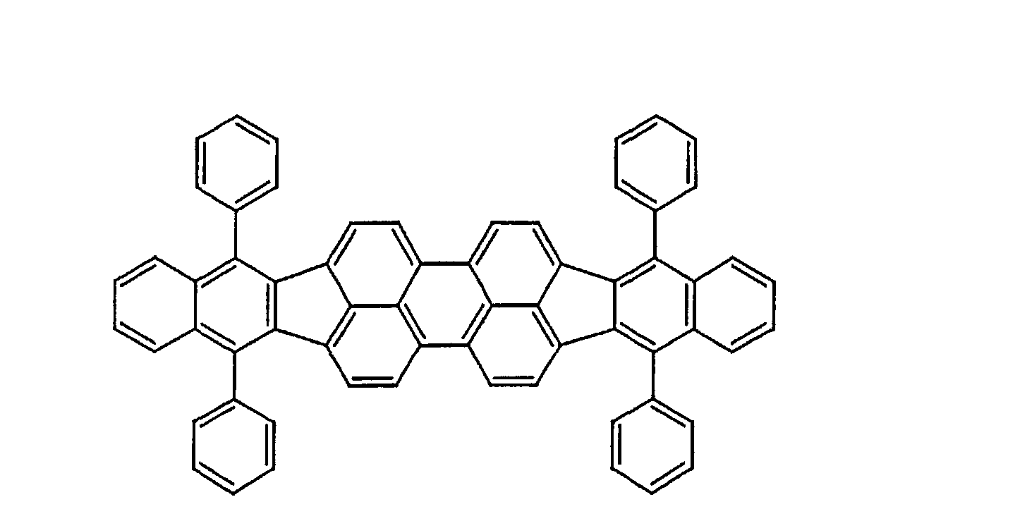
- JP-A 10-330295 and JP-A 11-233261 disclose organic EL devices having a light emitting layer in which a variety of host materials are doped with dibenzo[f,f']diindeno[1,2,3-cd:1',2',3'-1m]perylene derivatives derived from benzofluoranthene.
- light emitting materials disclosed heretofore include condensed polycyclic aromatic compounds (JP-A 5-32966 and 5-214334). Also dopant materials proposed heretofore include various condensed polycyclic aromatic compounds (JP-A 5-258859).
- An object of the invention is to provide a compound for use in organic EL devices capable of light emission to a satisfactory luminance, especially at a long wavelength, and with a high color purity, especially a color purity sufficient for use in full color displays, and having a sufficient durability to sustain such improved light emission performance over a long time as well as an organic EL device using the same.
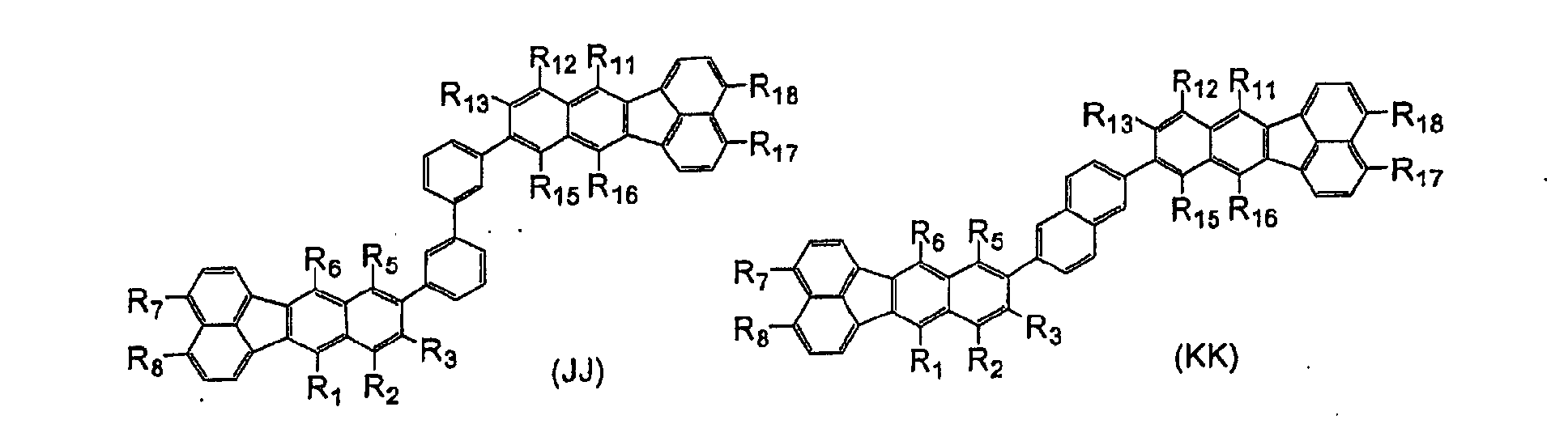
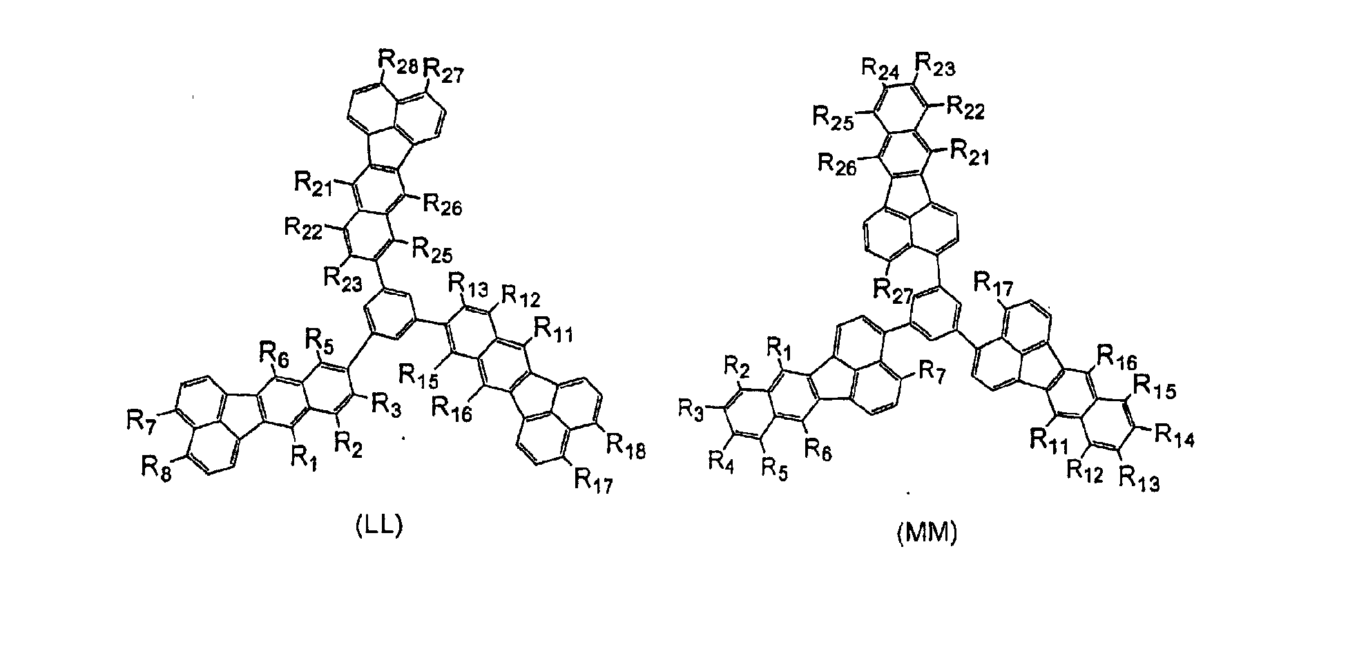
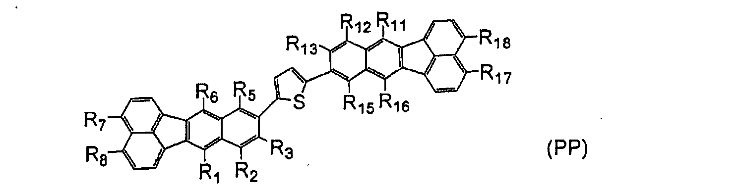
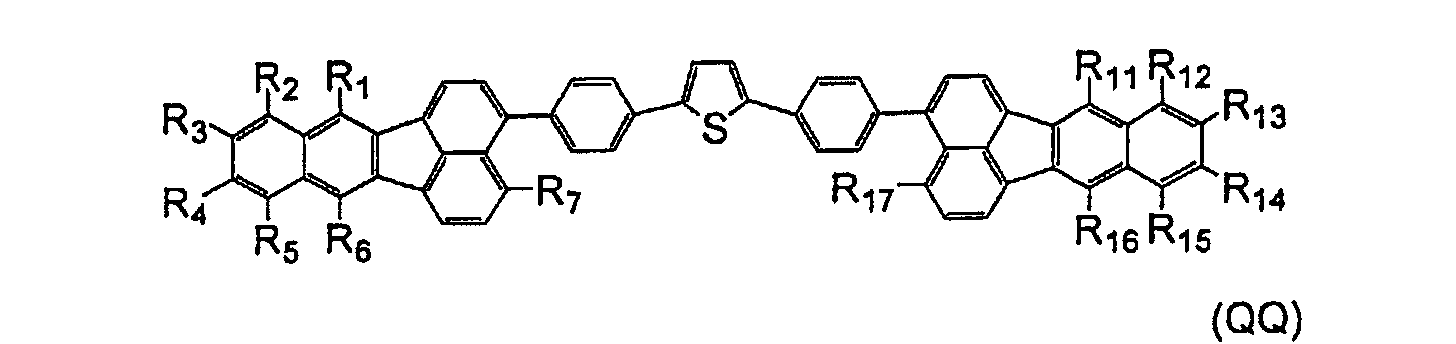
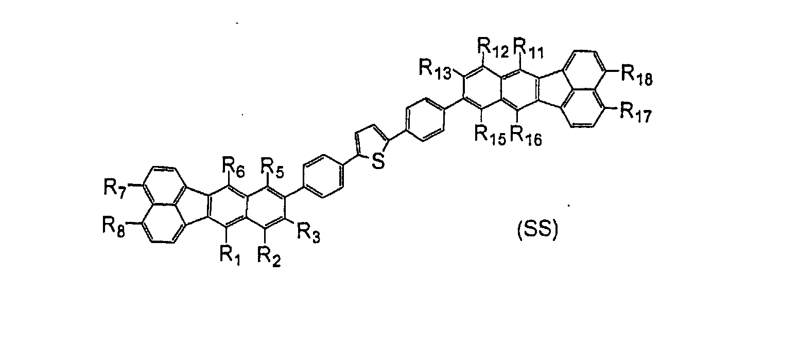
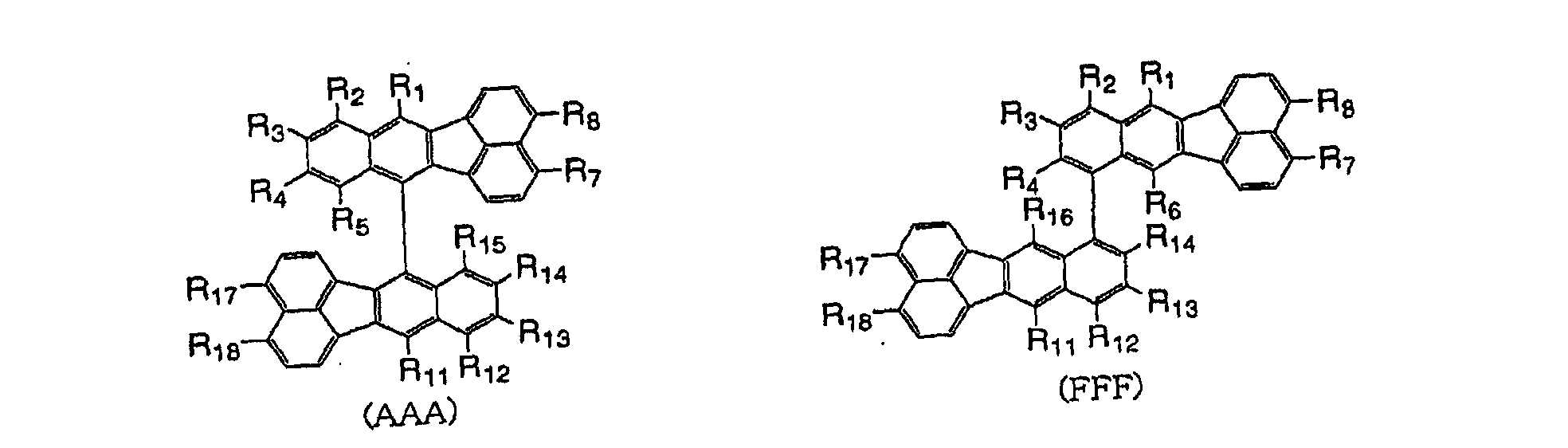
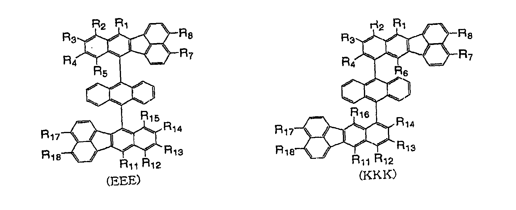
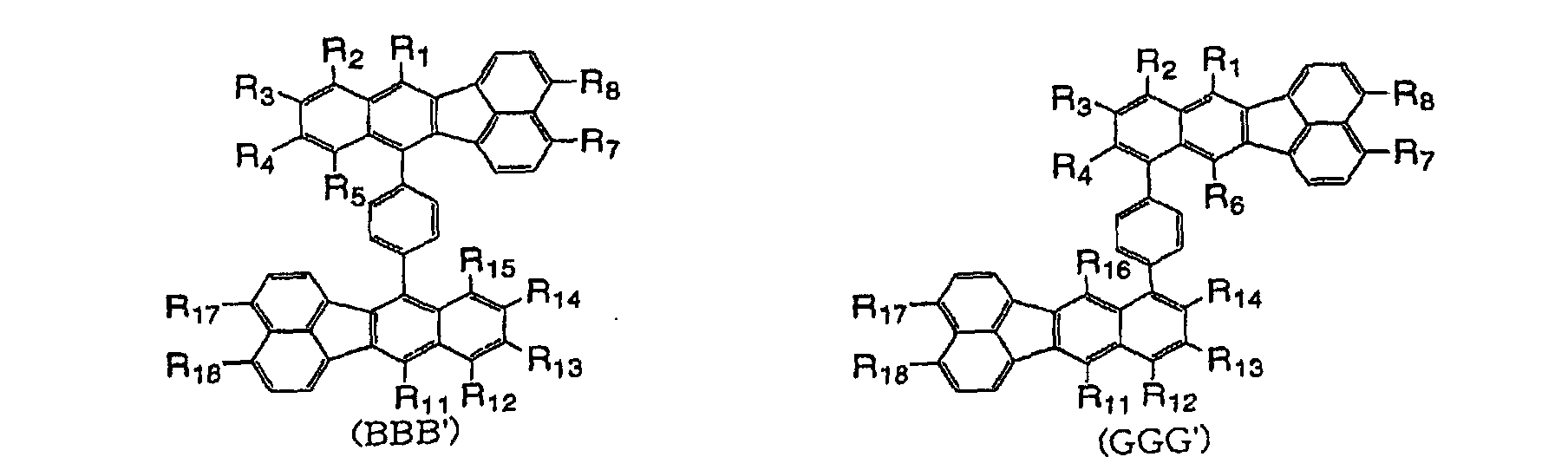
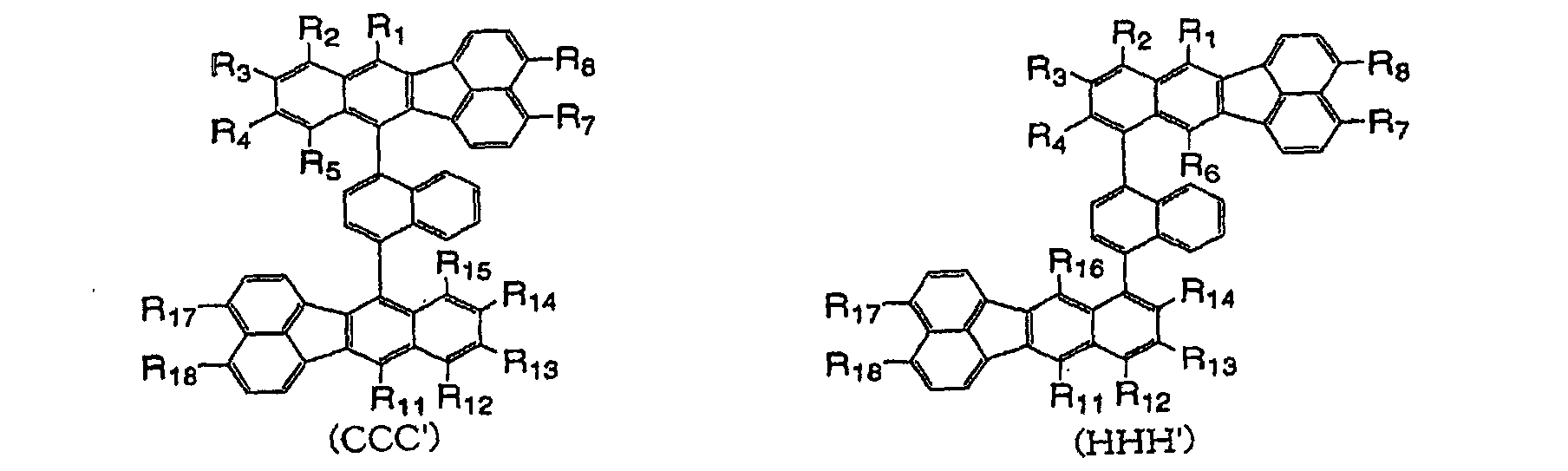
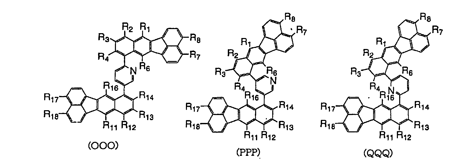
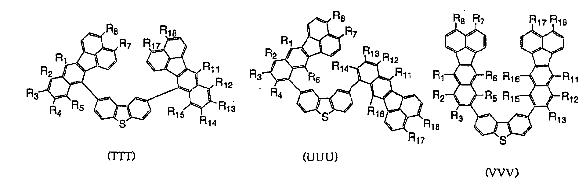
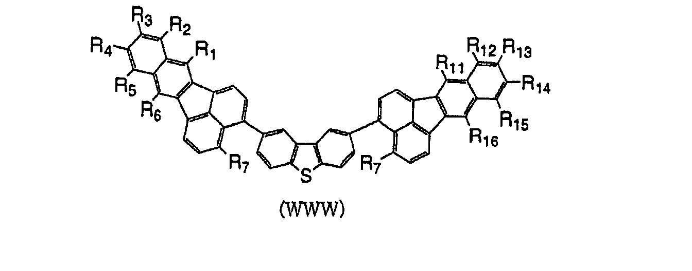
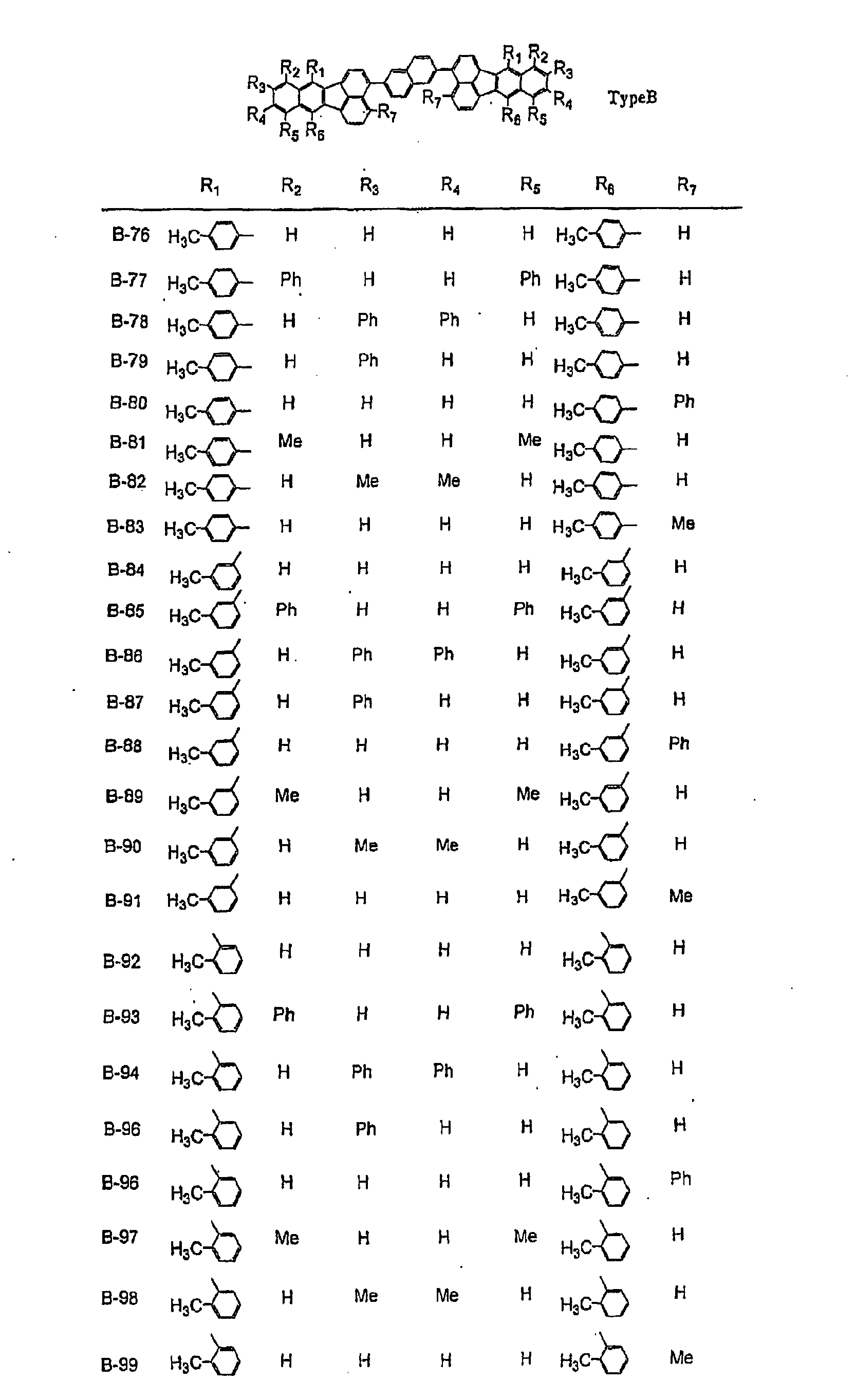
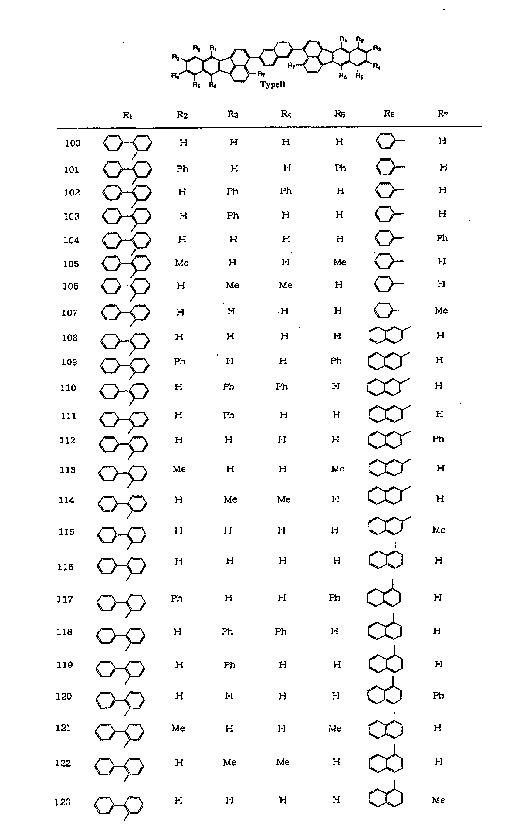
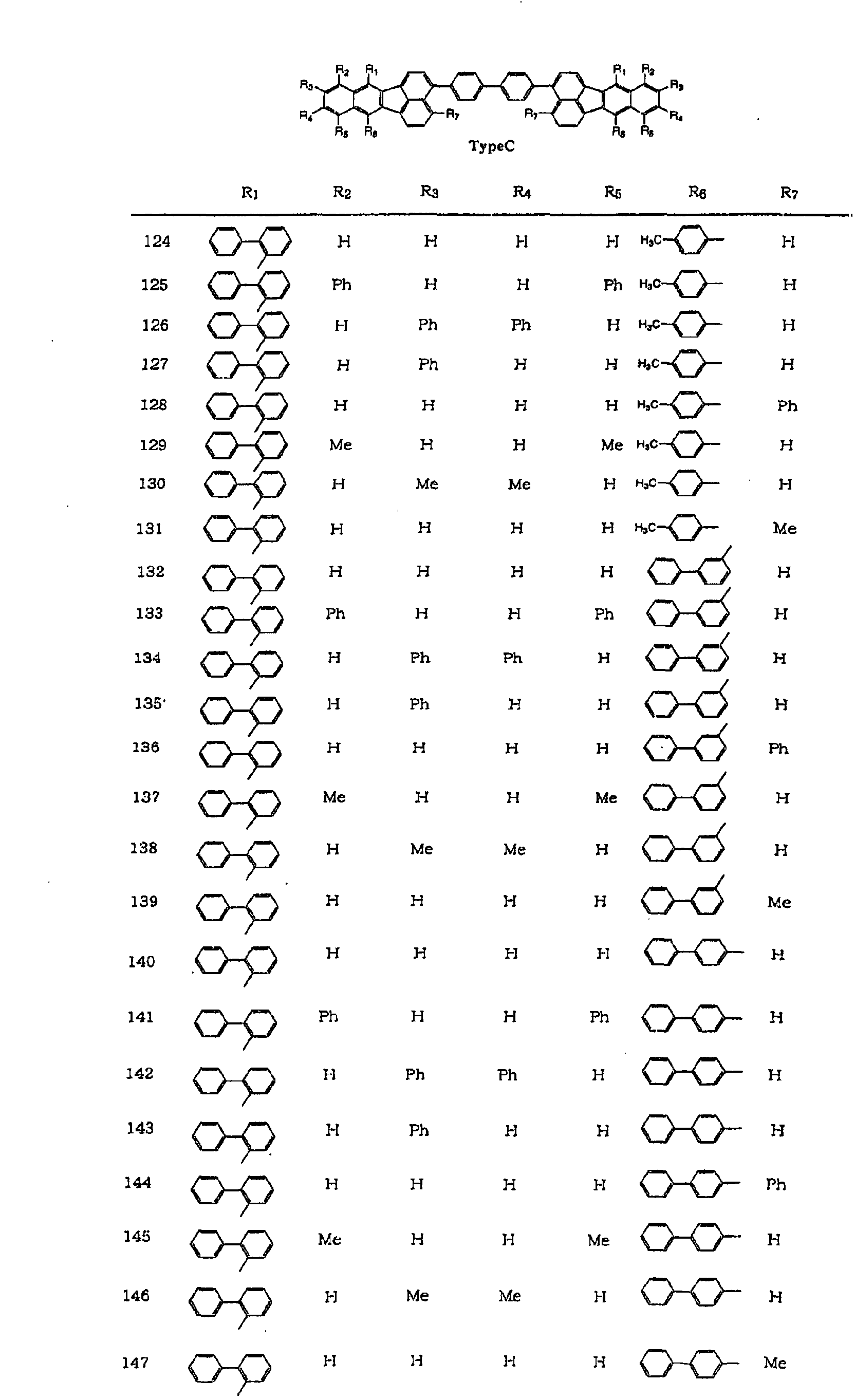
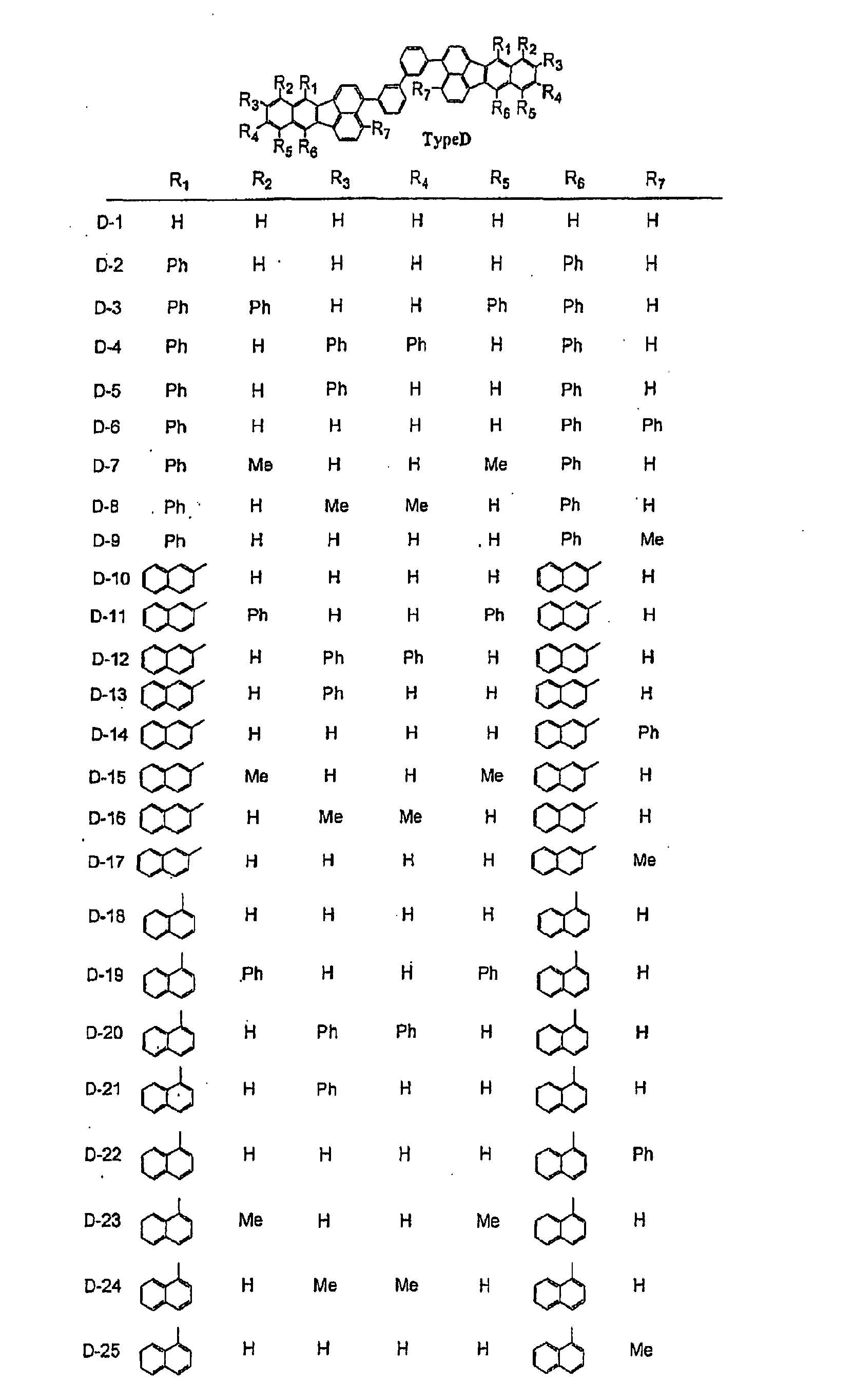
- the compounds for use in organic EL devices according to the invention have a basic skeleton of the following formula (1).
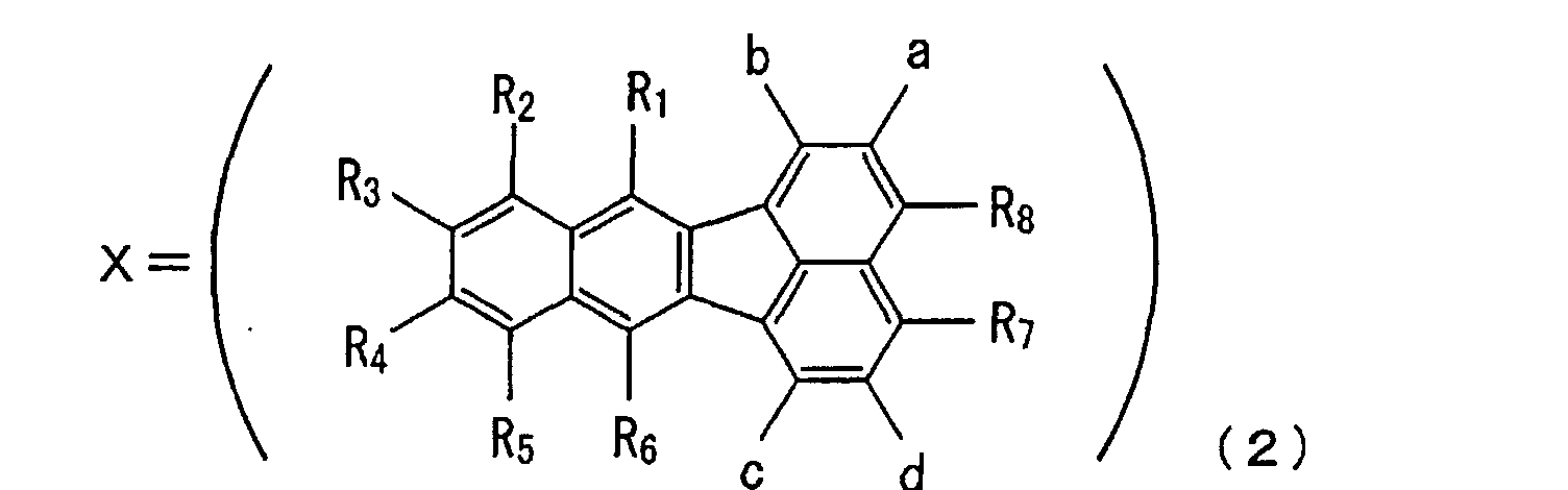
- X is a compound of the following formula (2) and may be the same or different
- Y is a linking group selected from among a single bond, a substituted or unsubstituted aryl group, and a heterocyclic group
- n is an integer of 2 or 3.
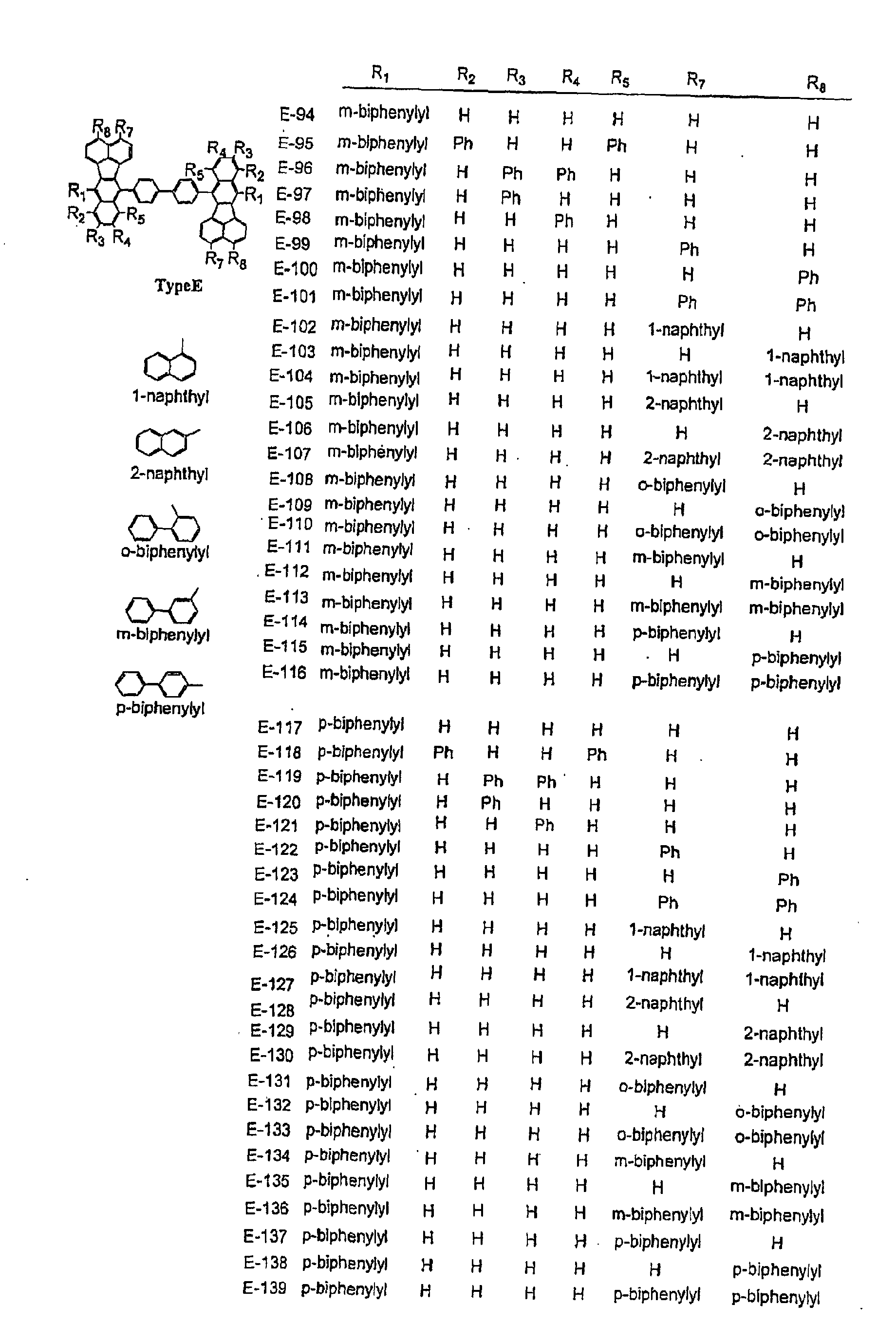
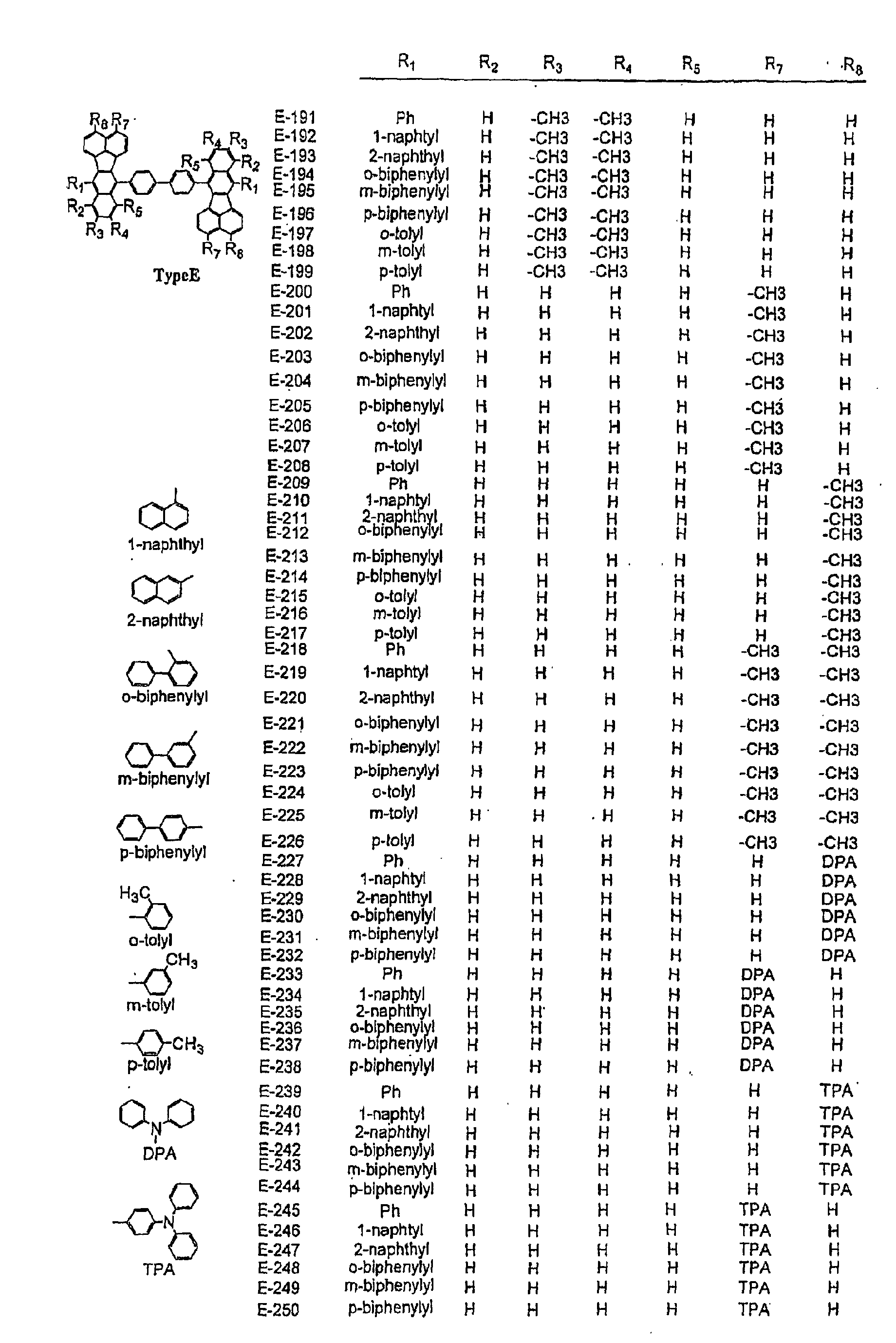
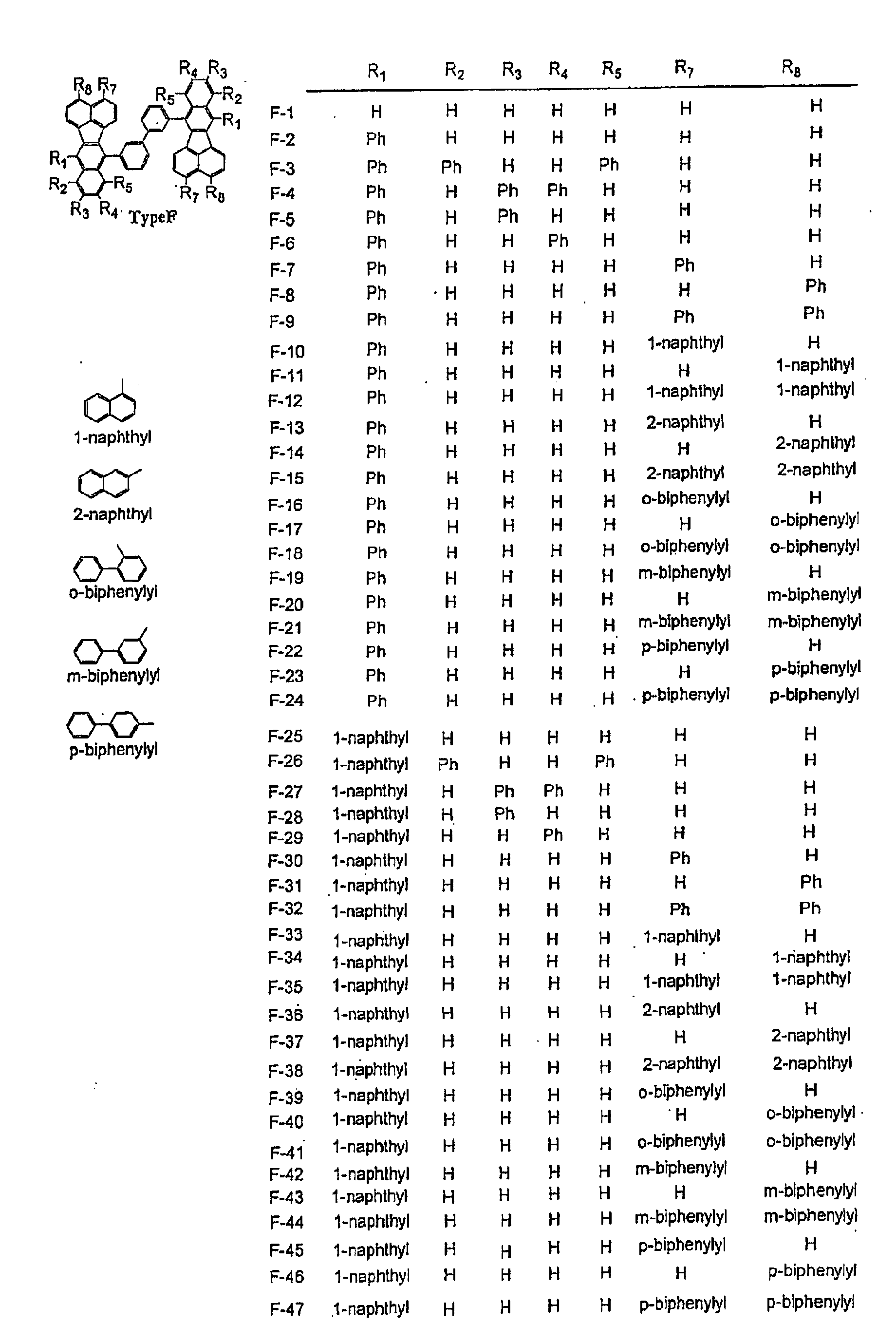
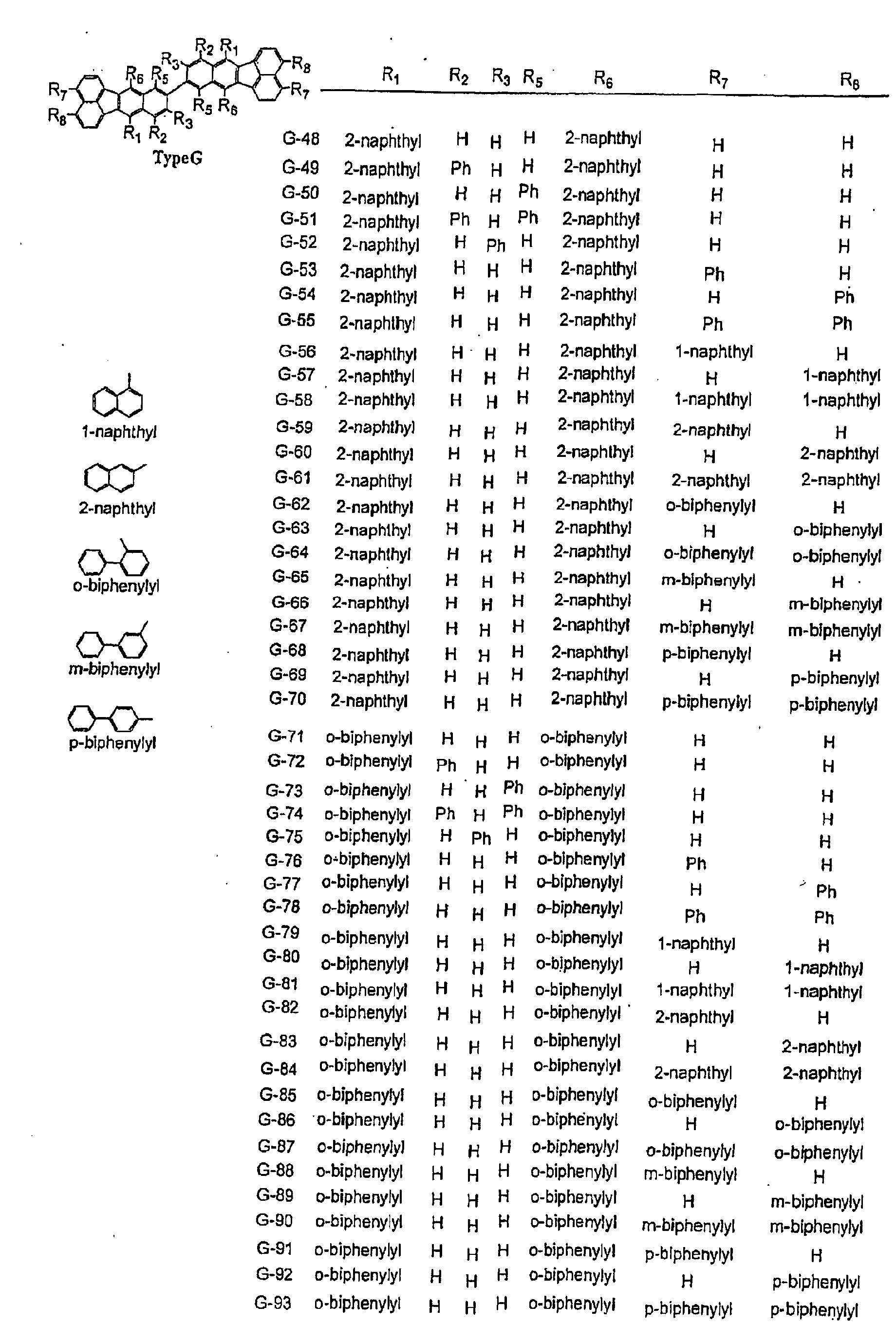
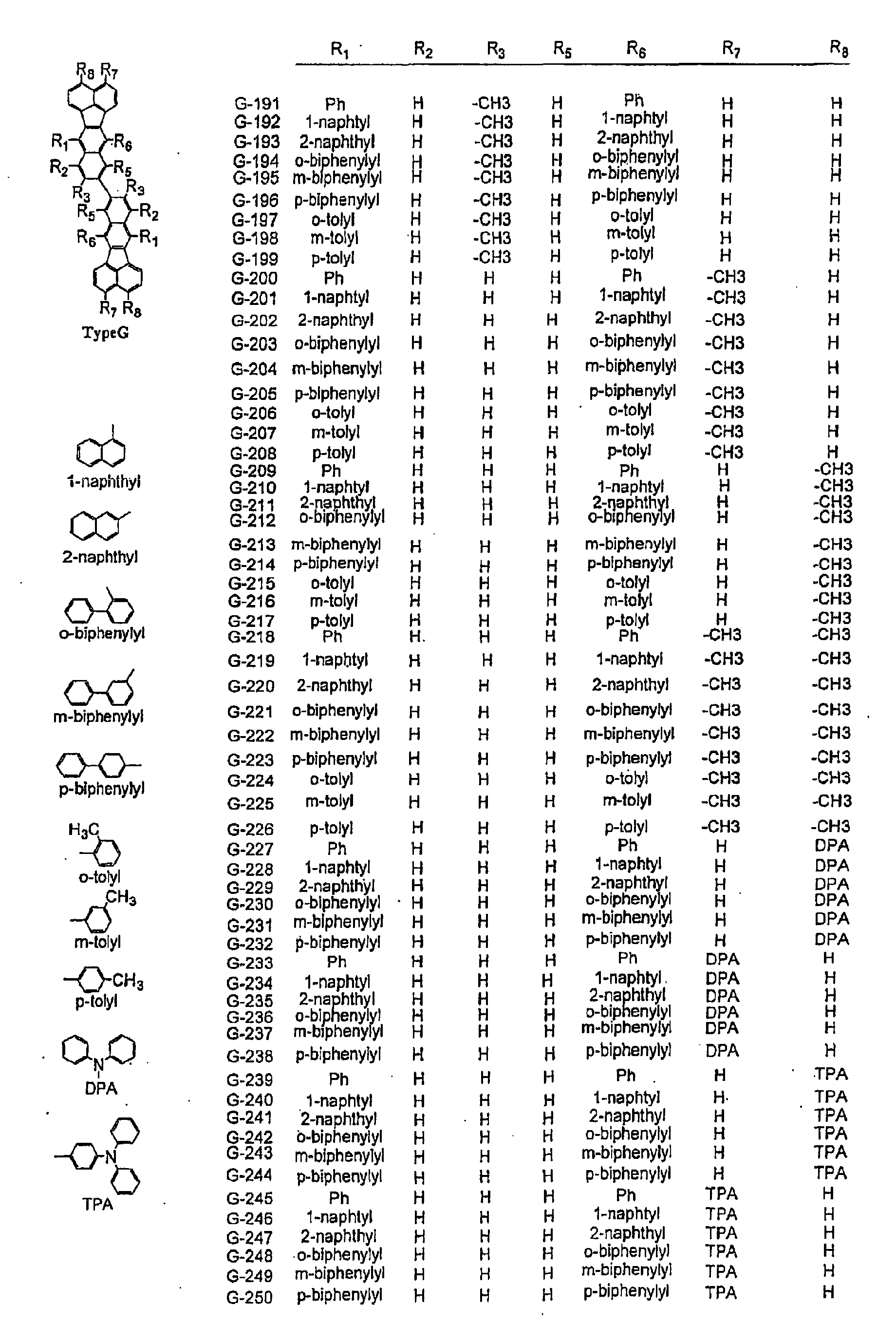
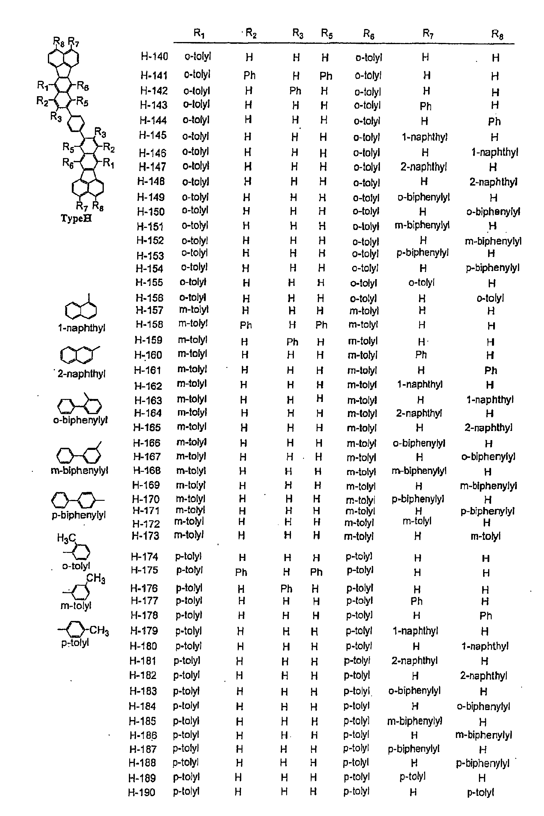
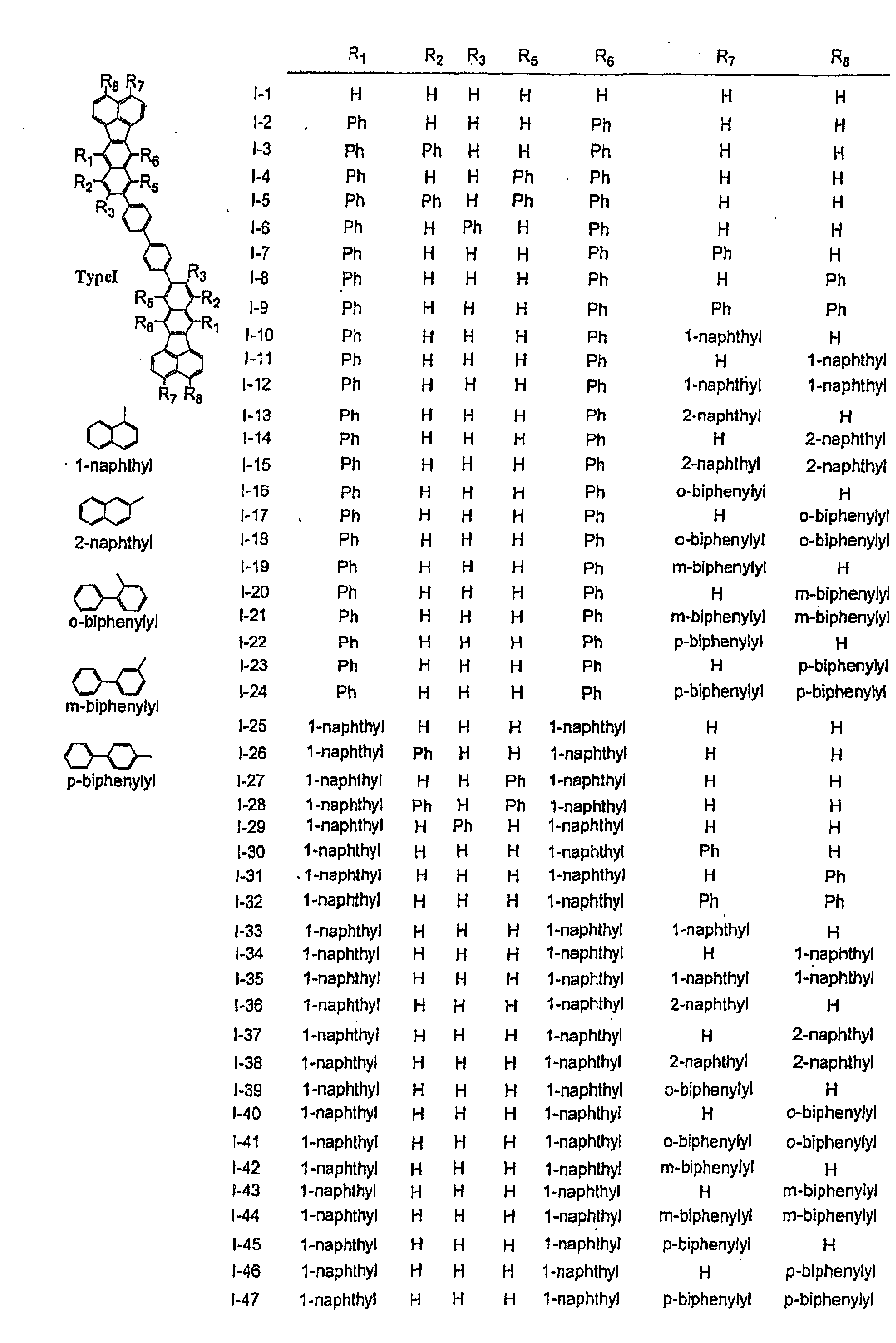
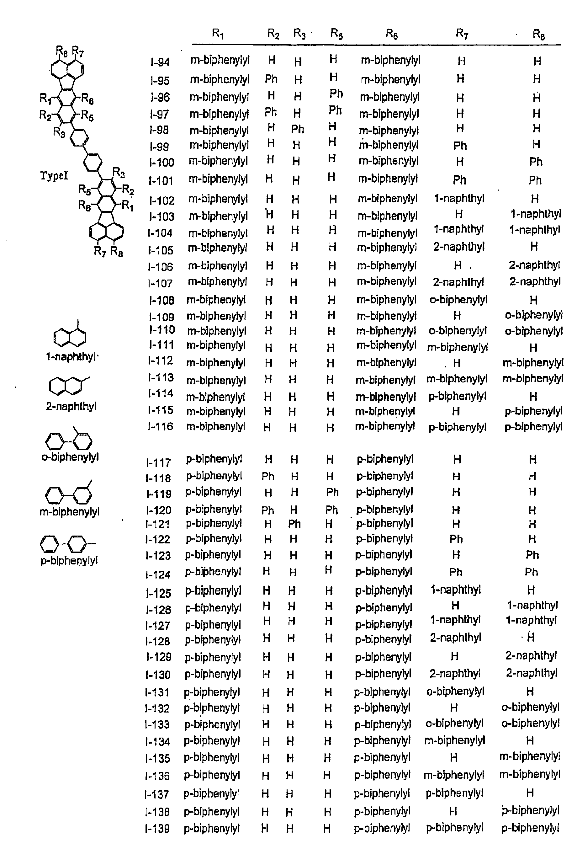
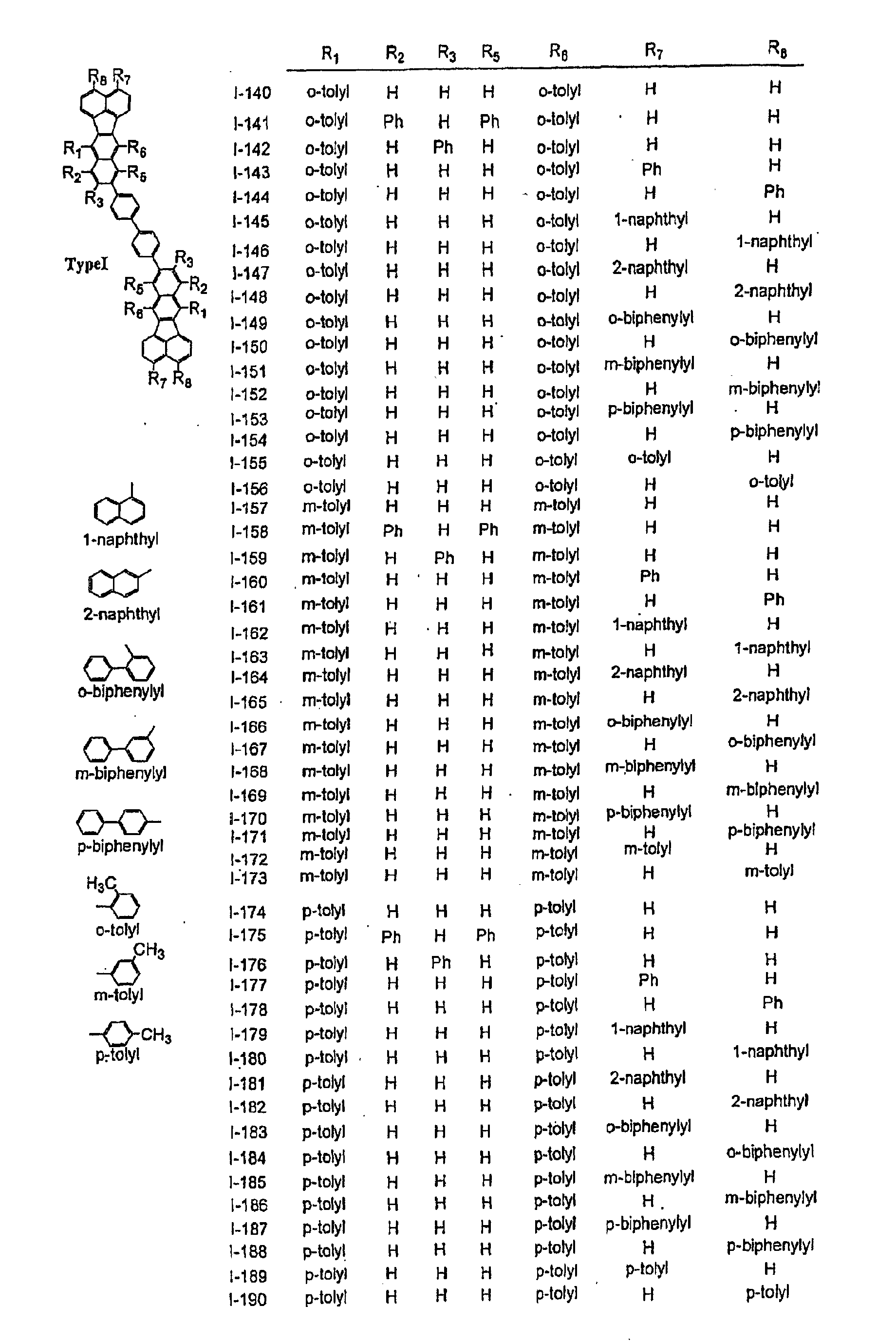
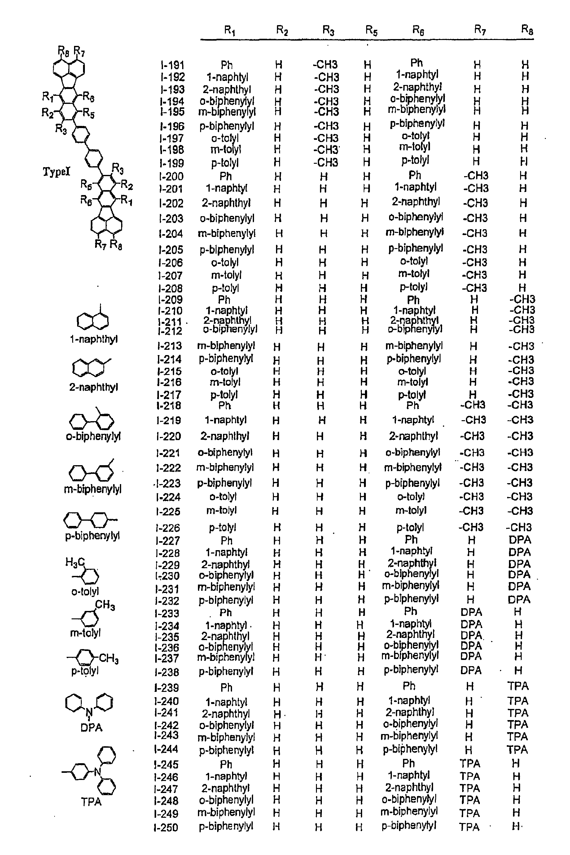
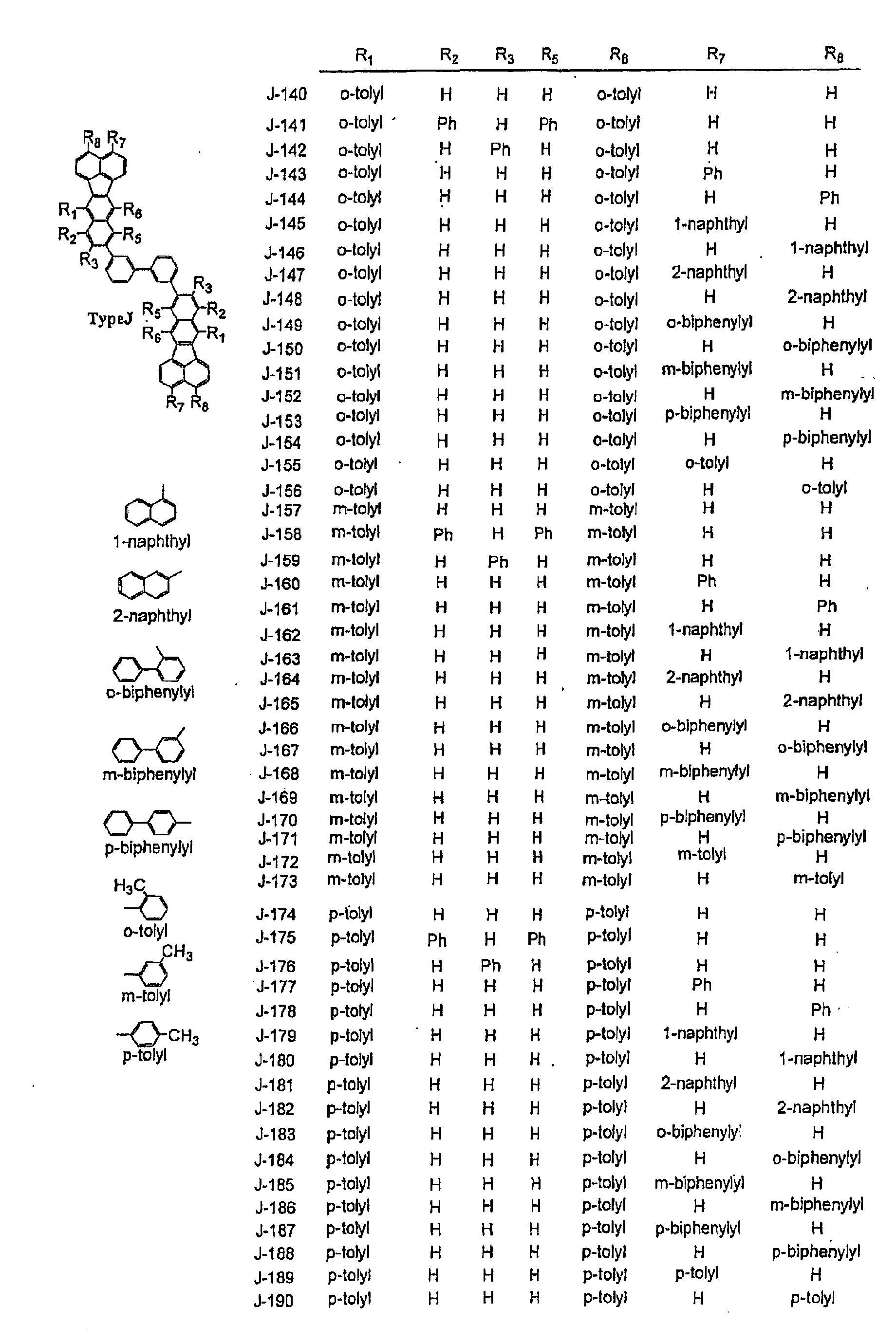
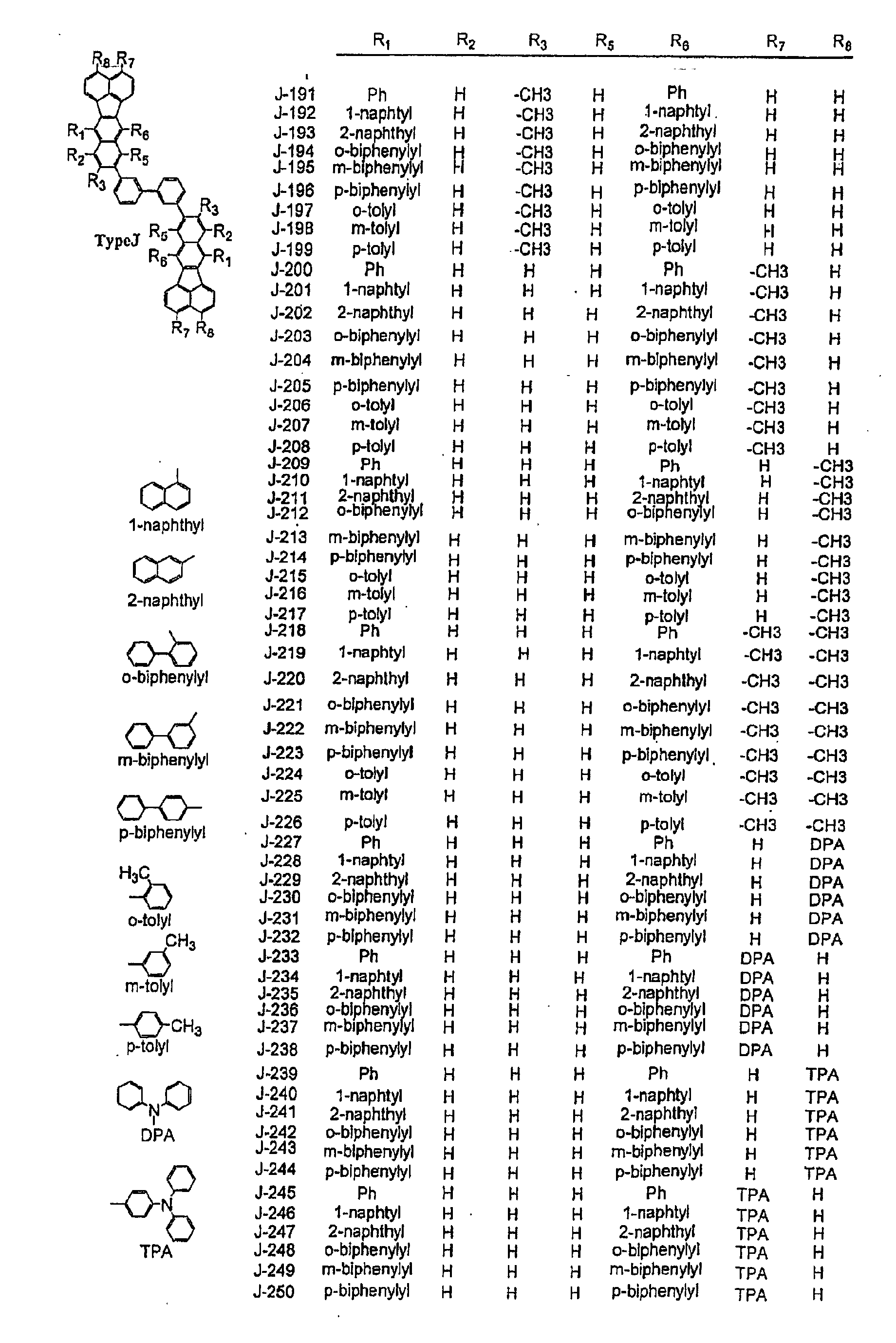
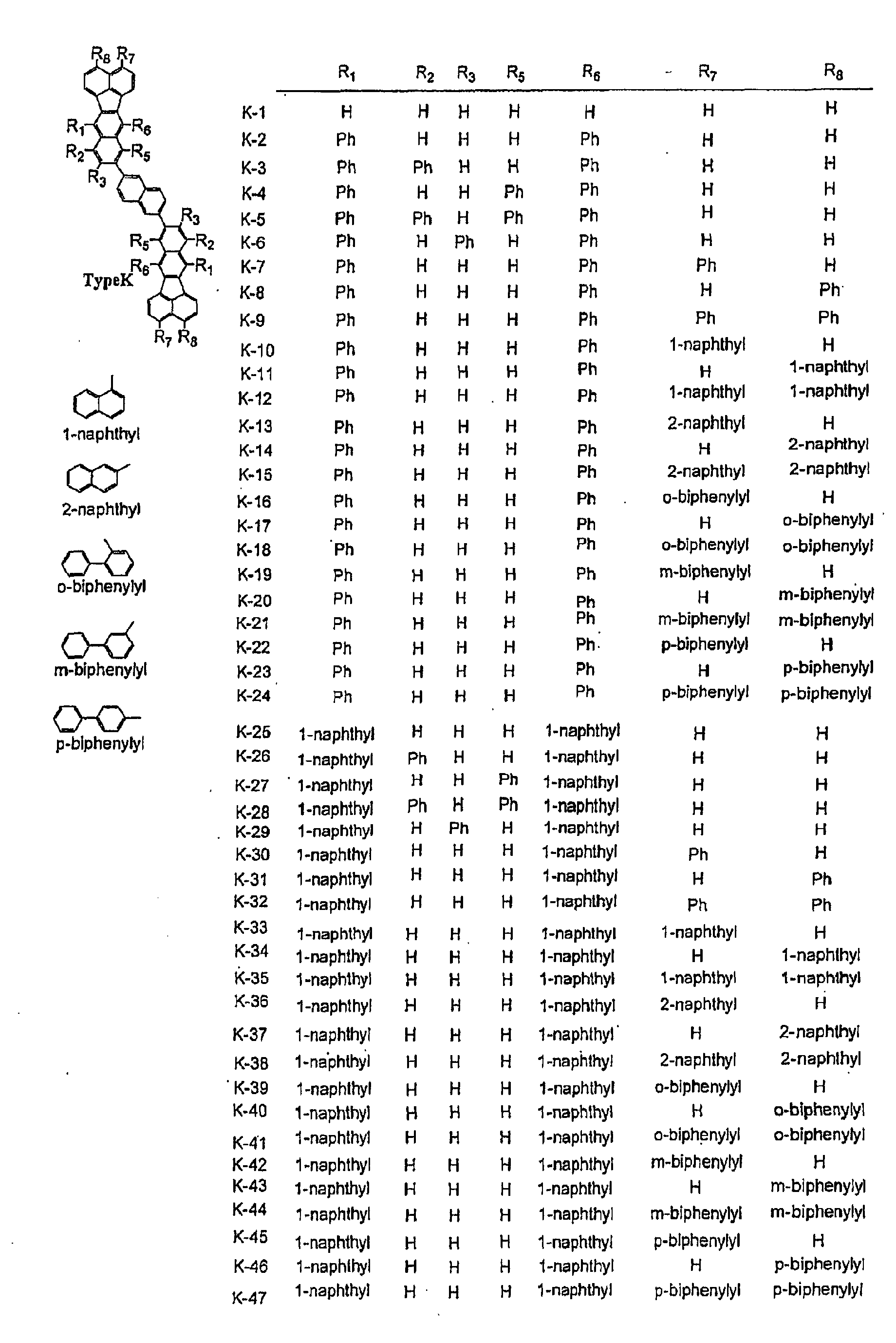
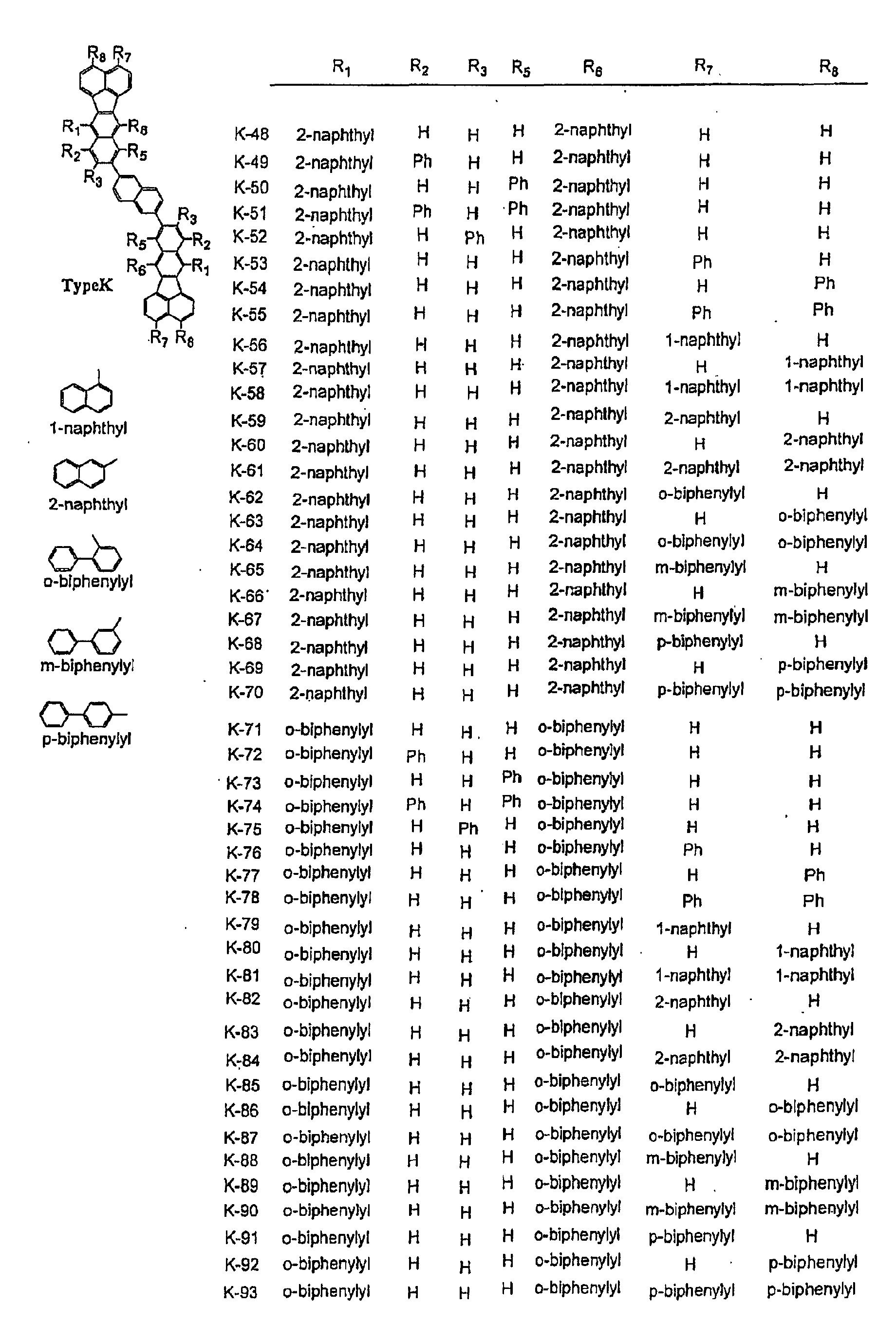
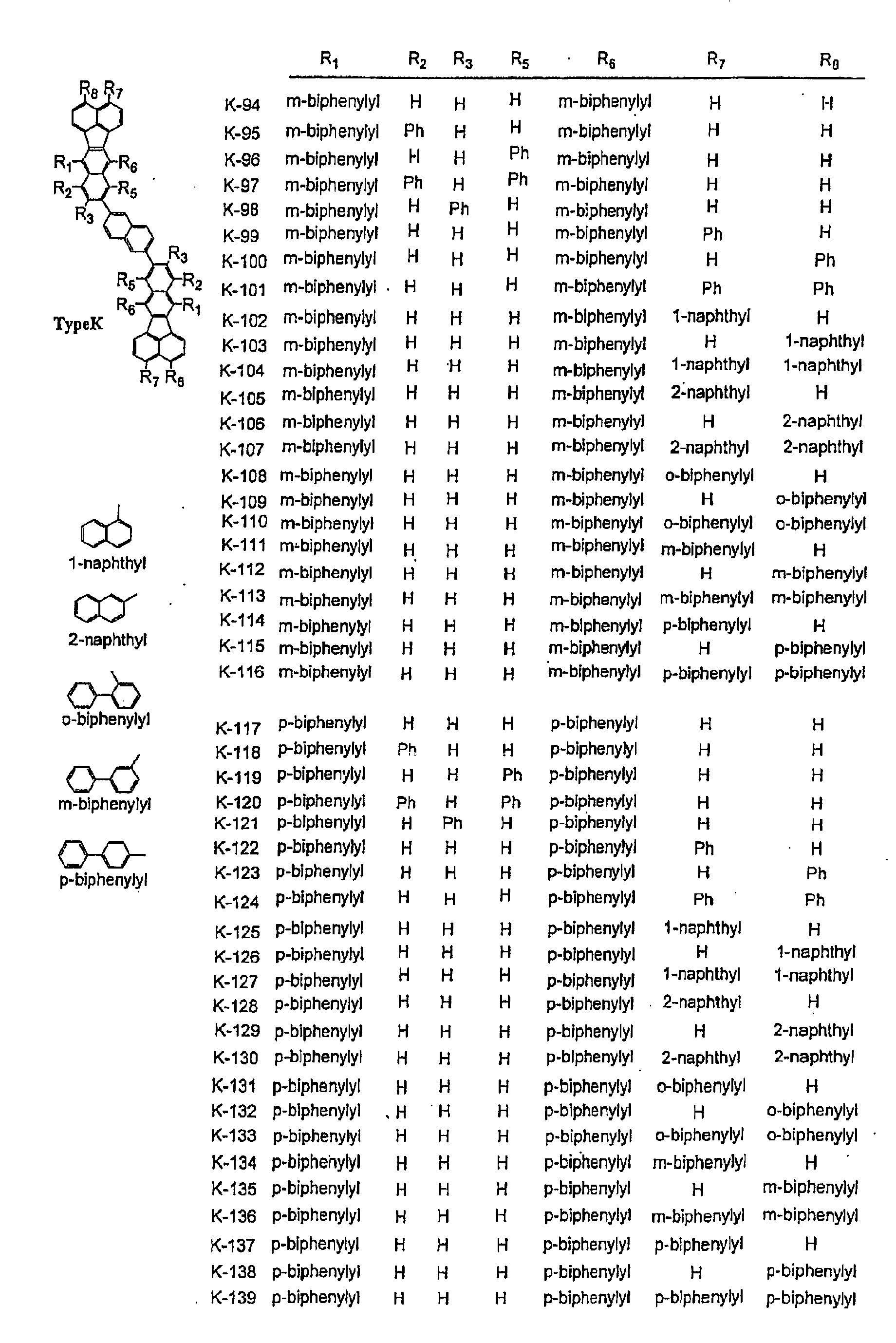
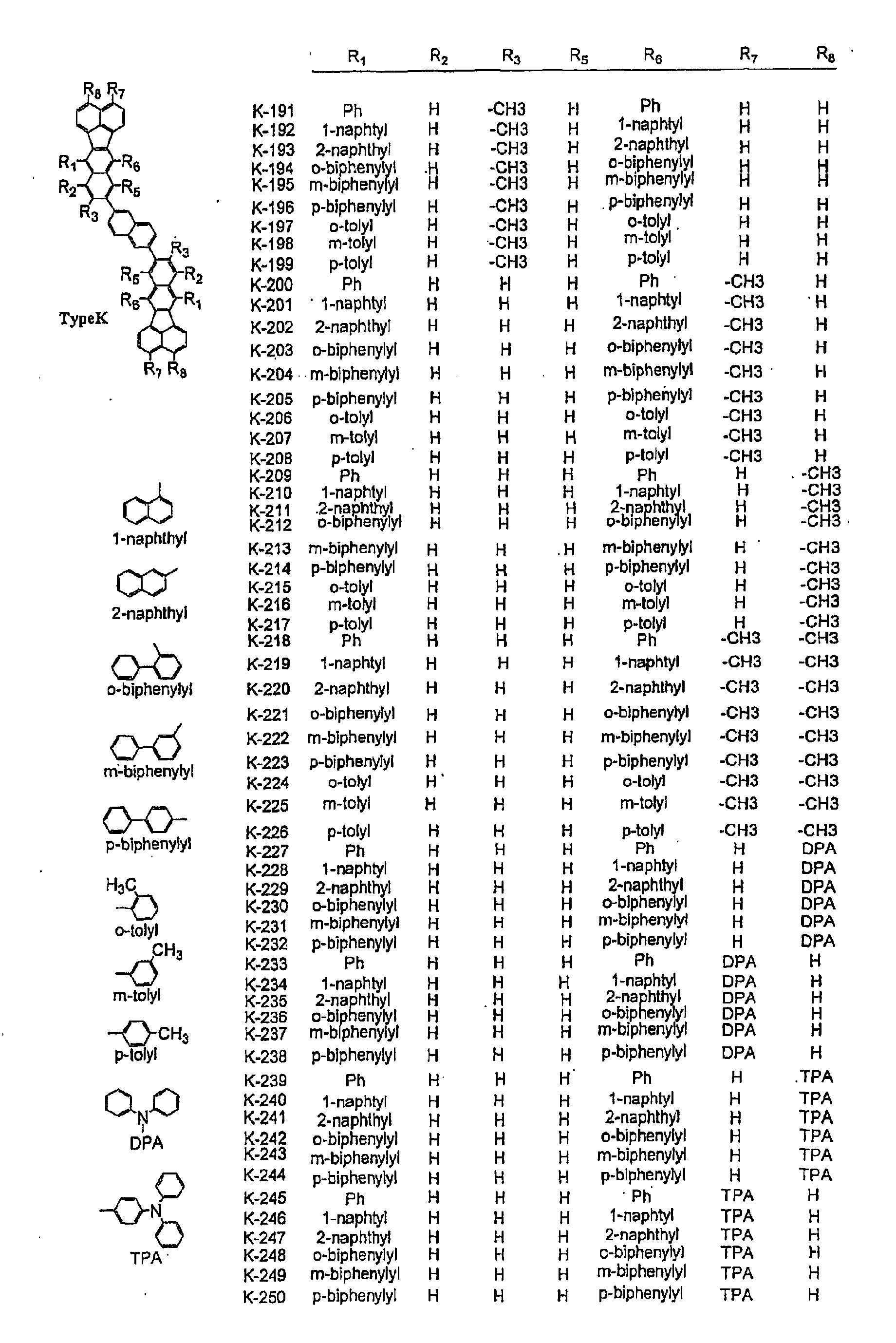
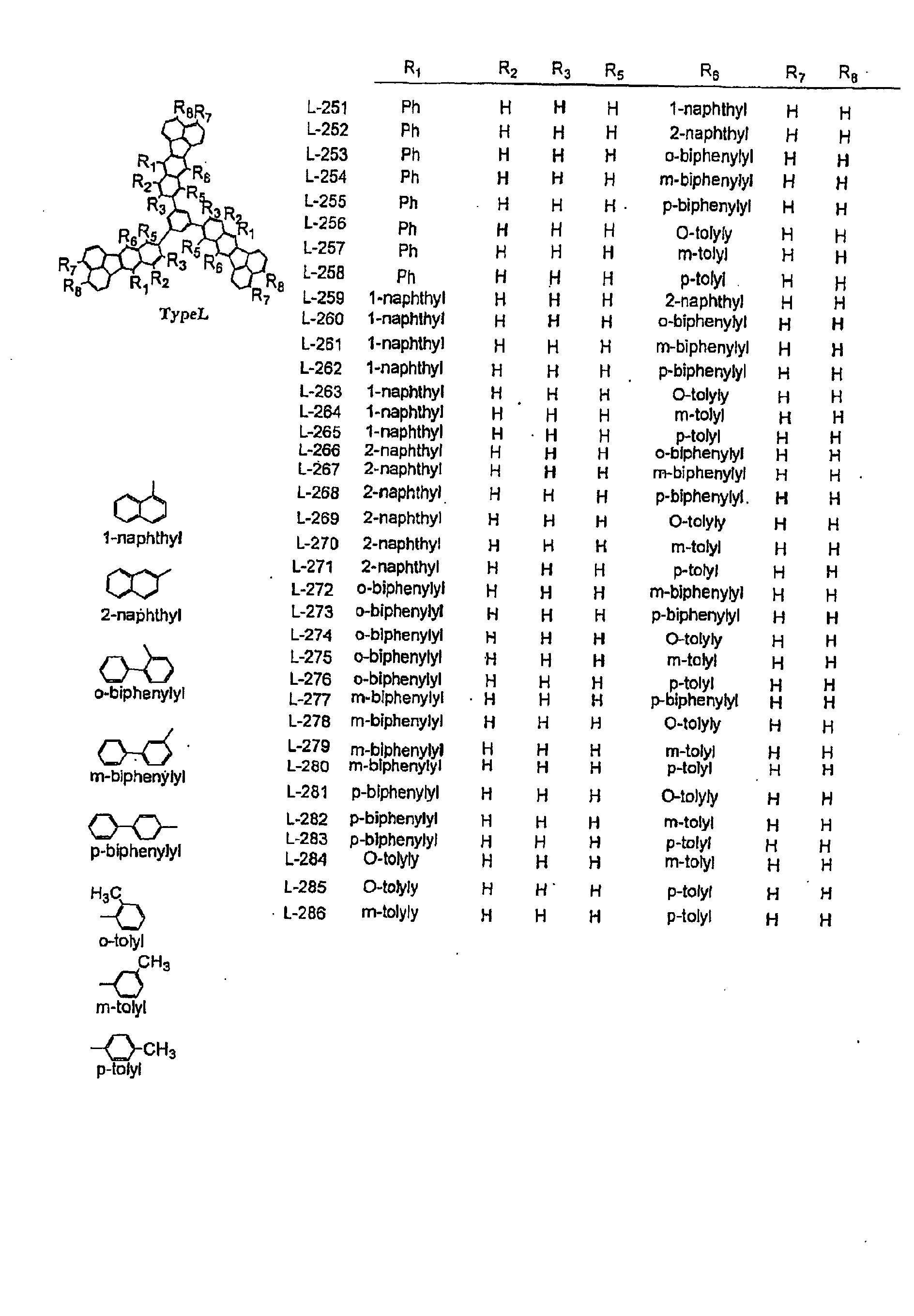
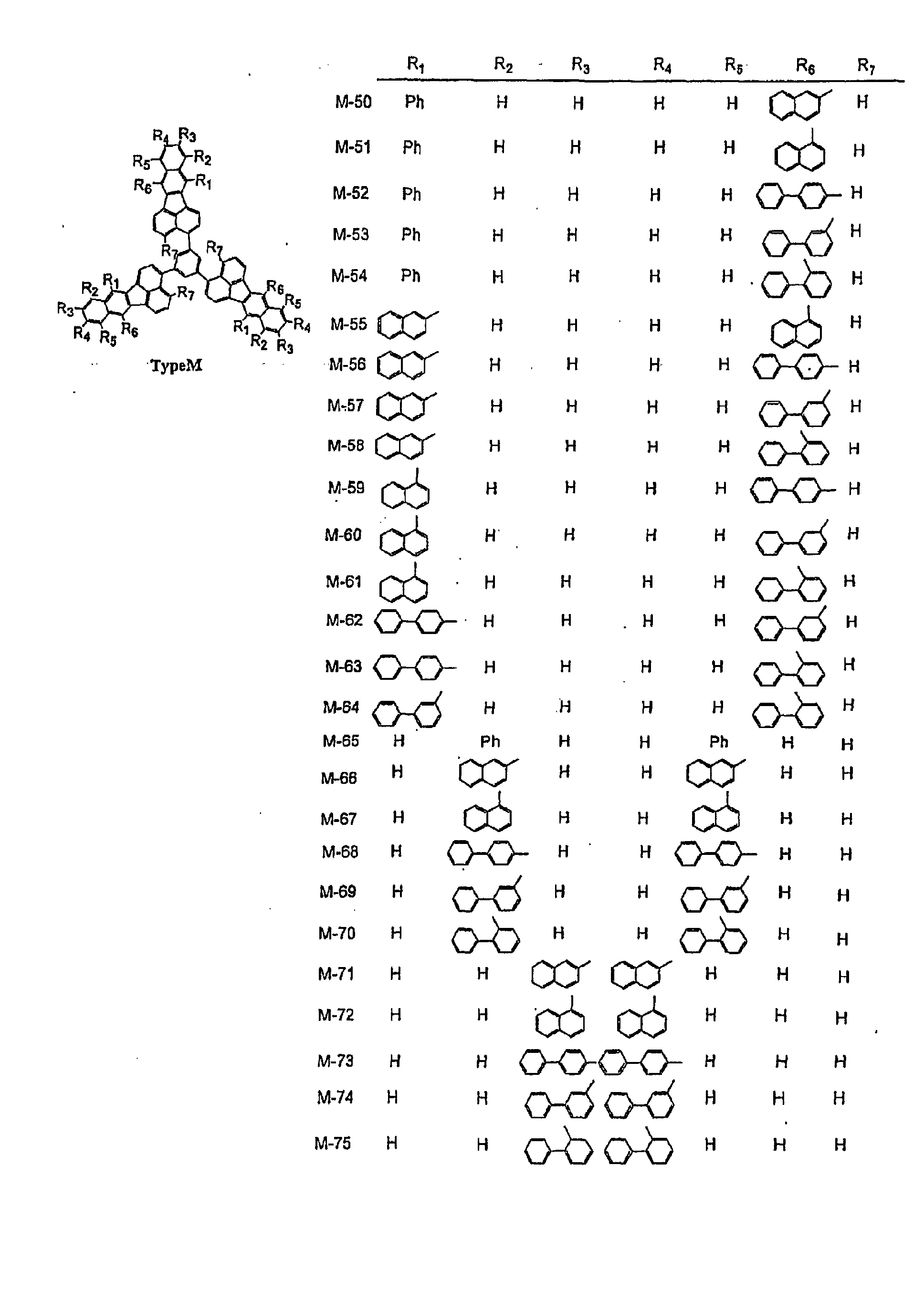
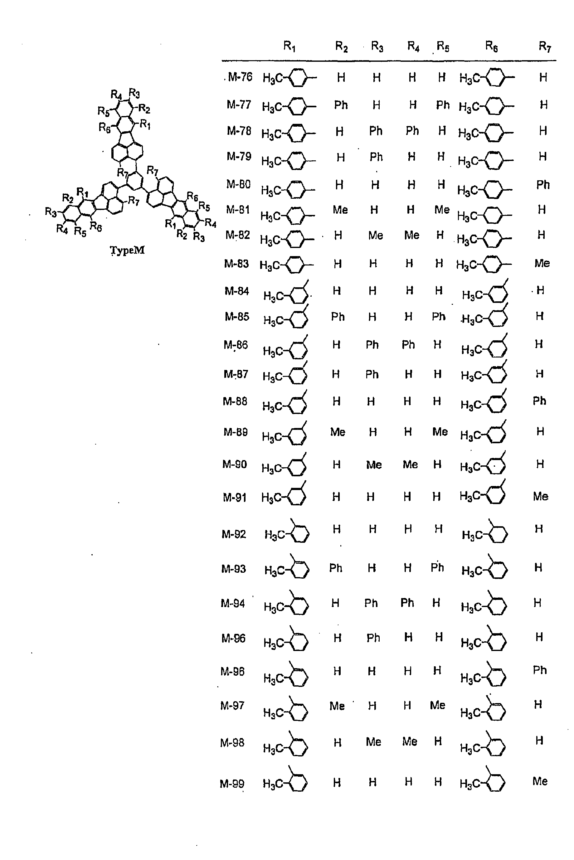
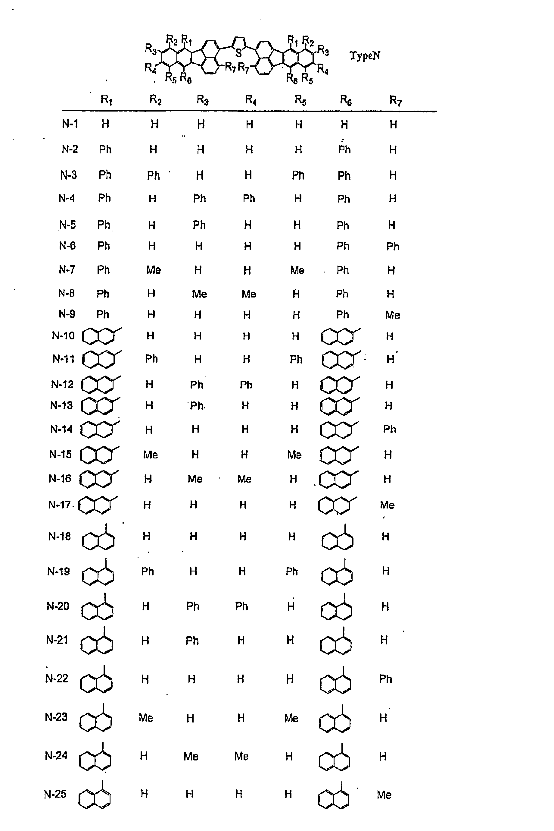
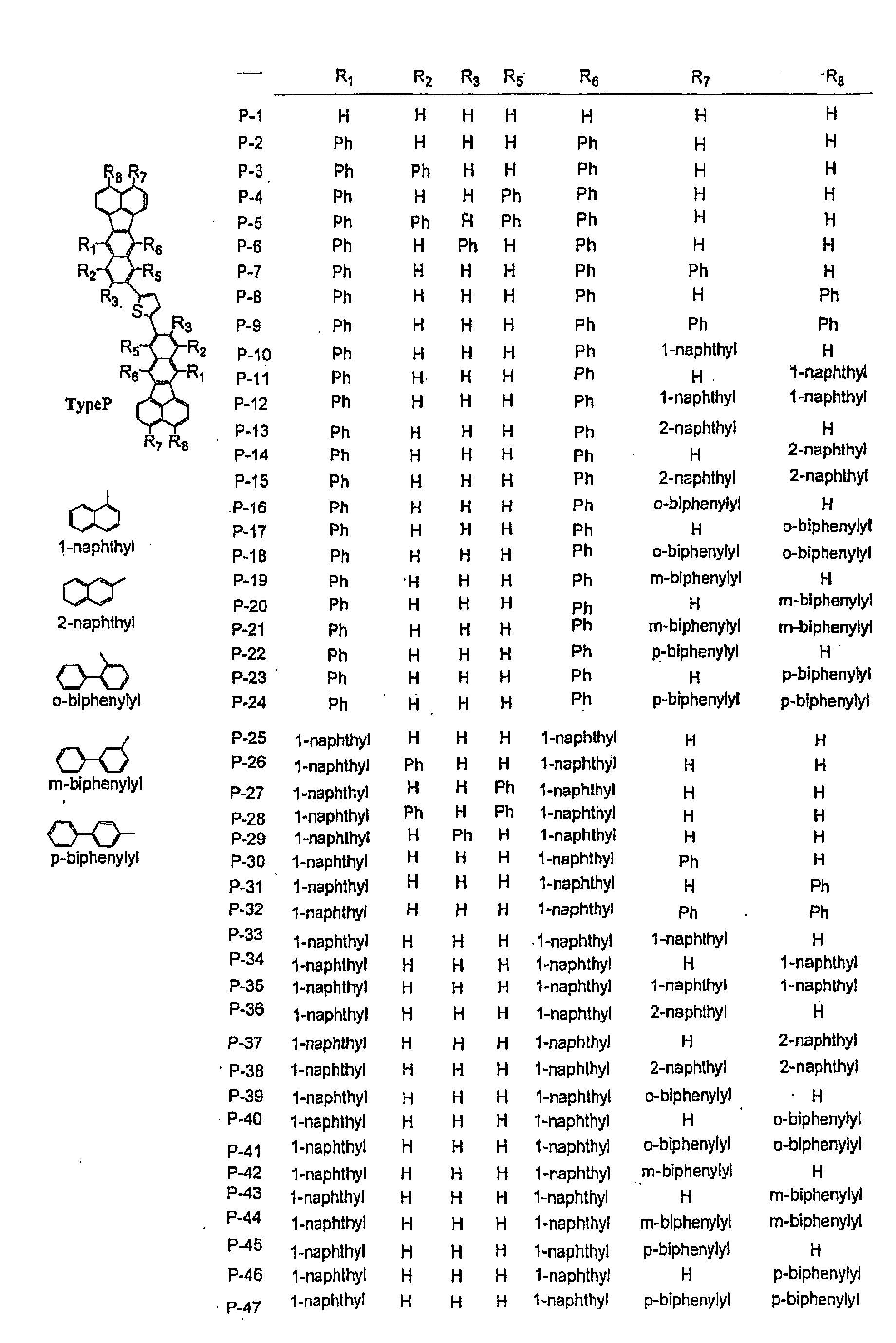
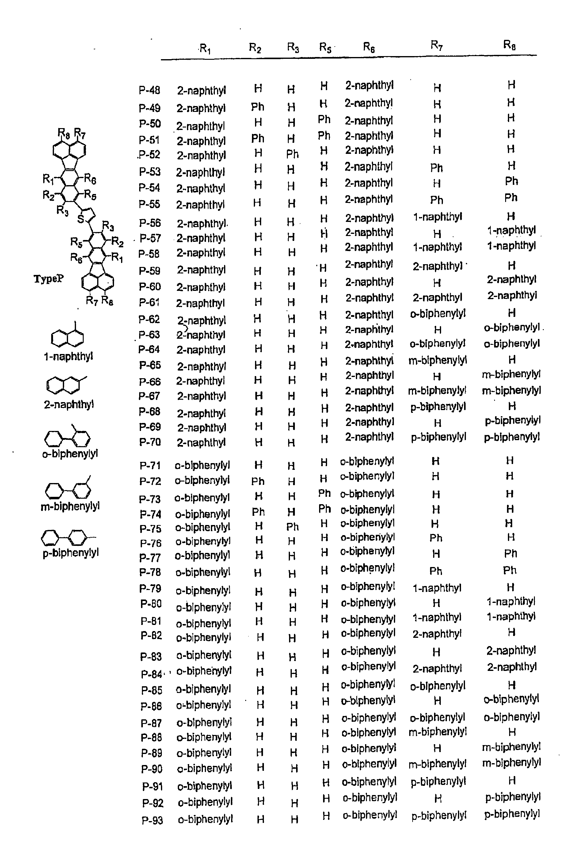
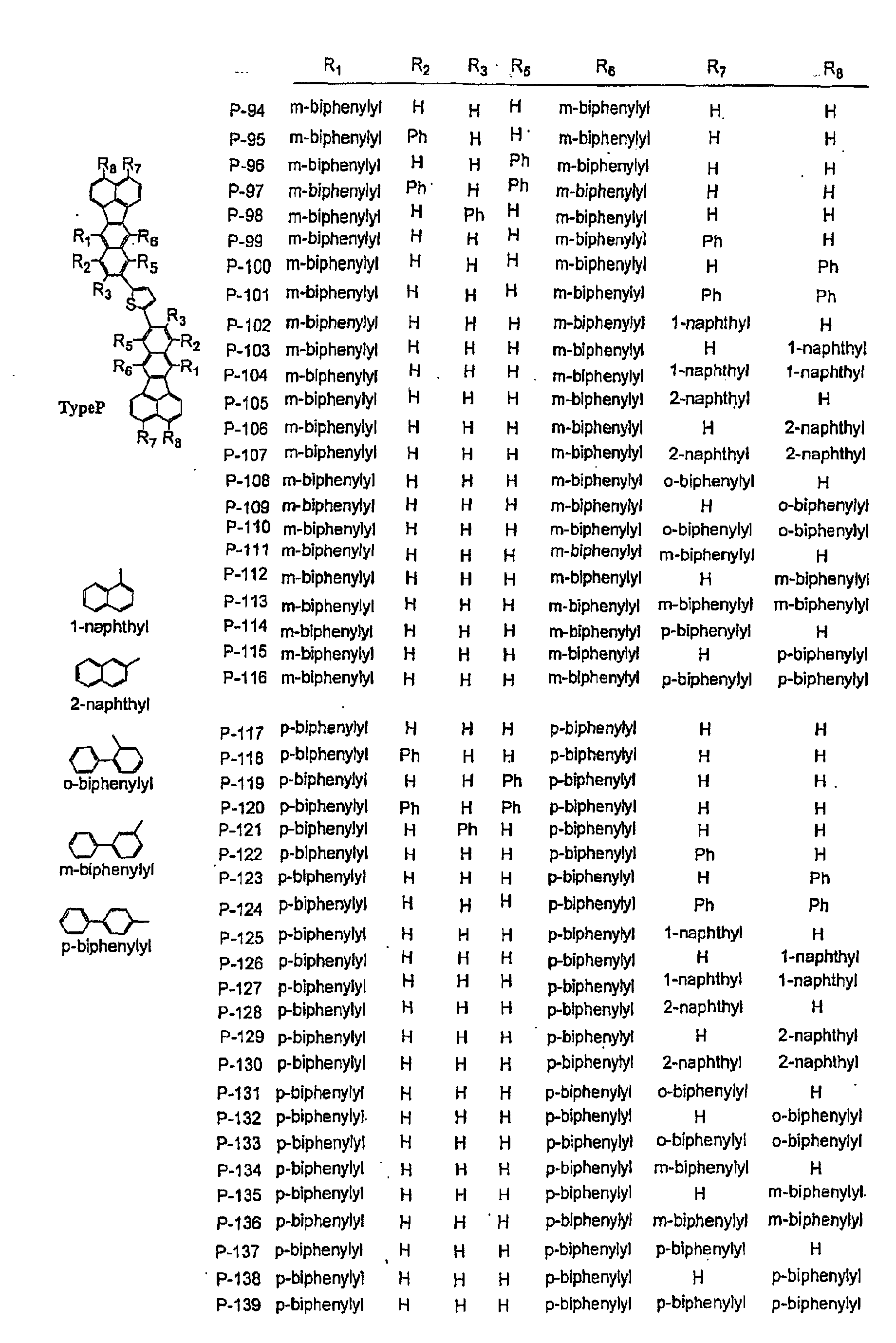
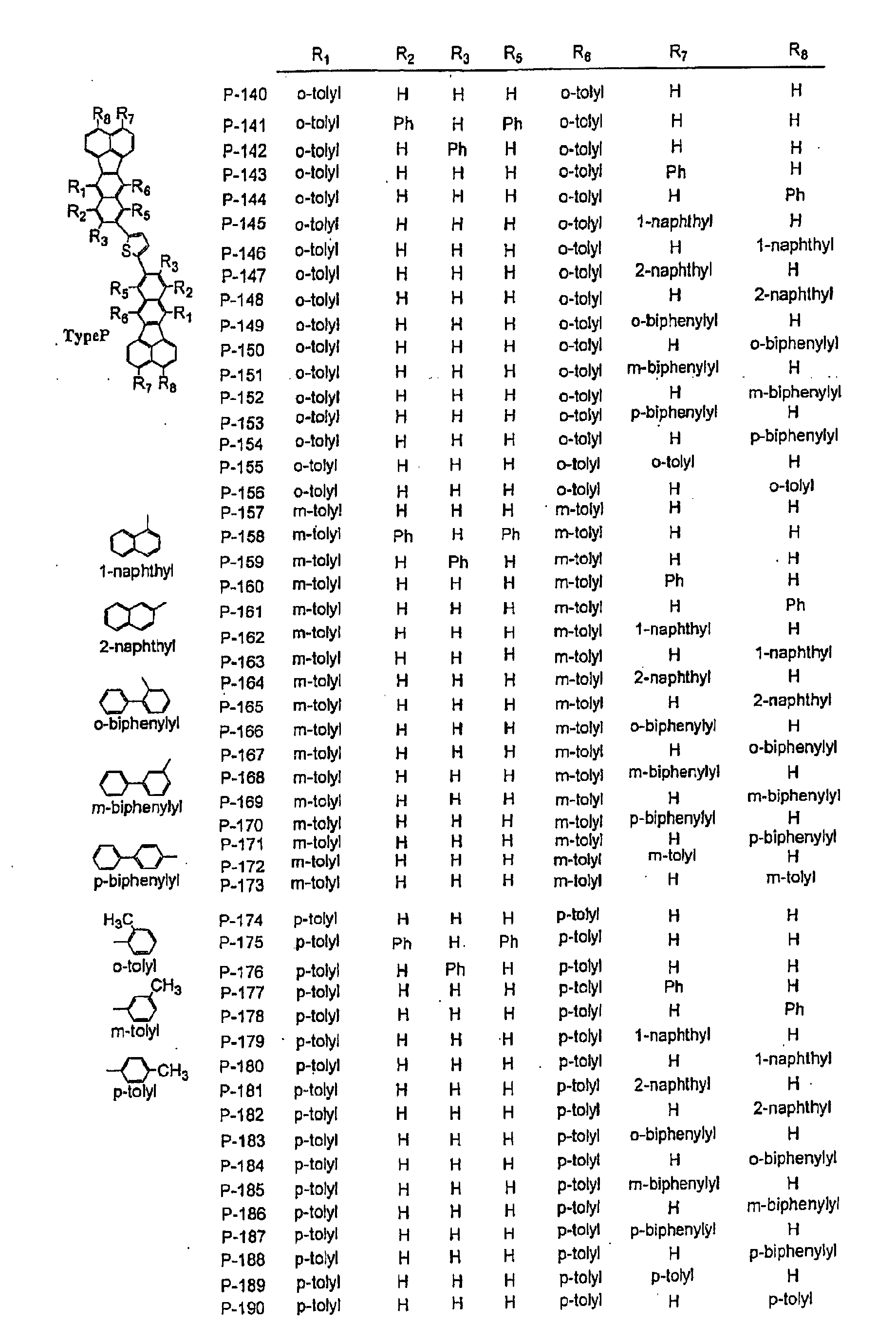
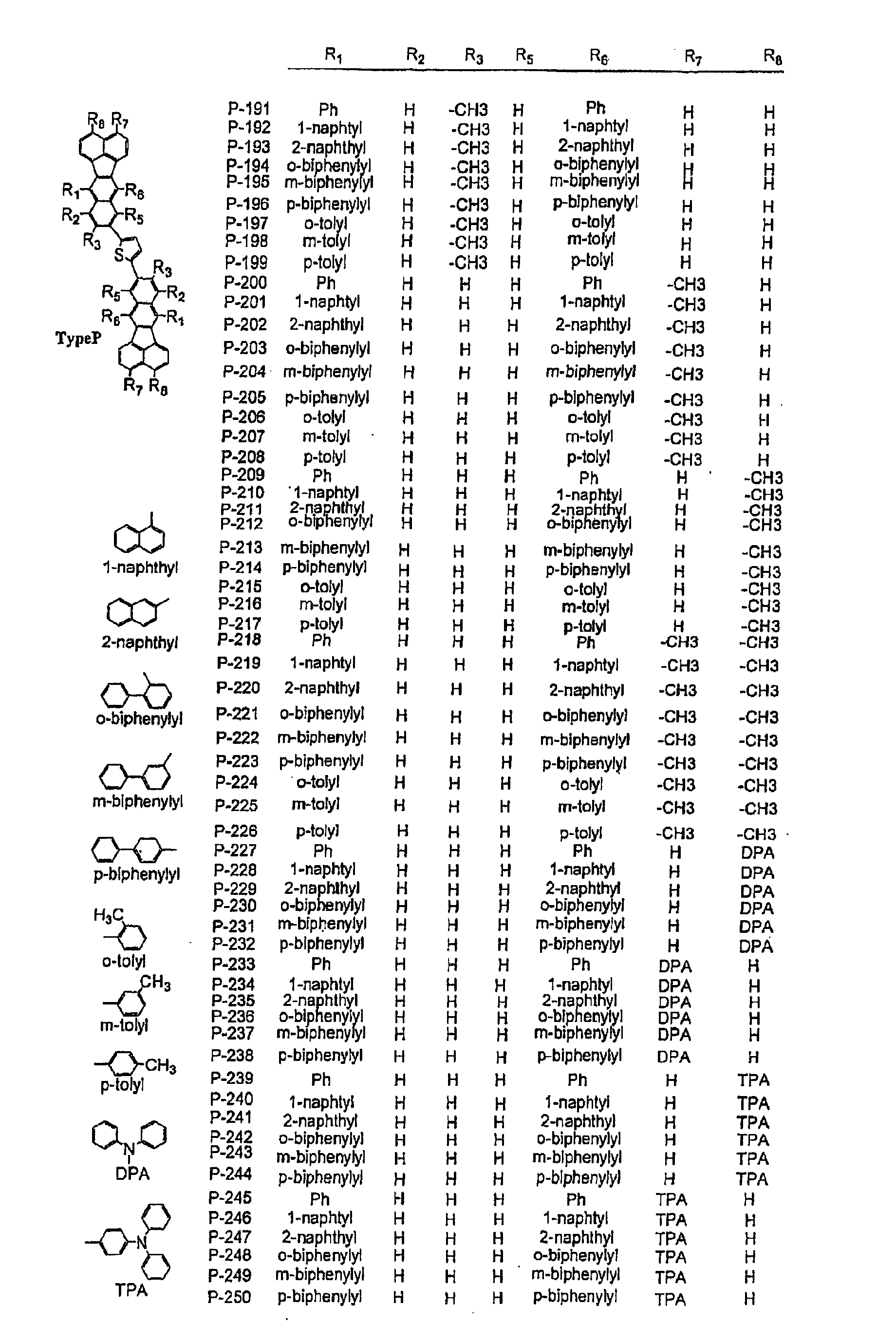
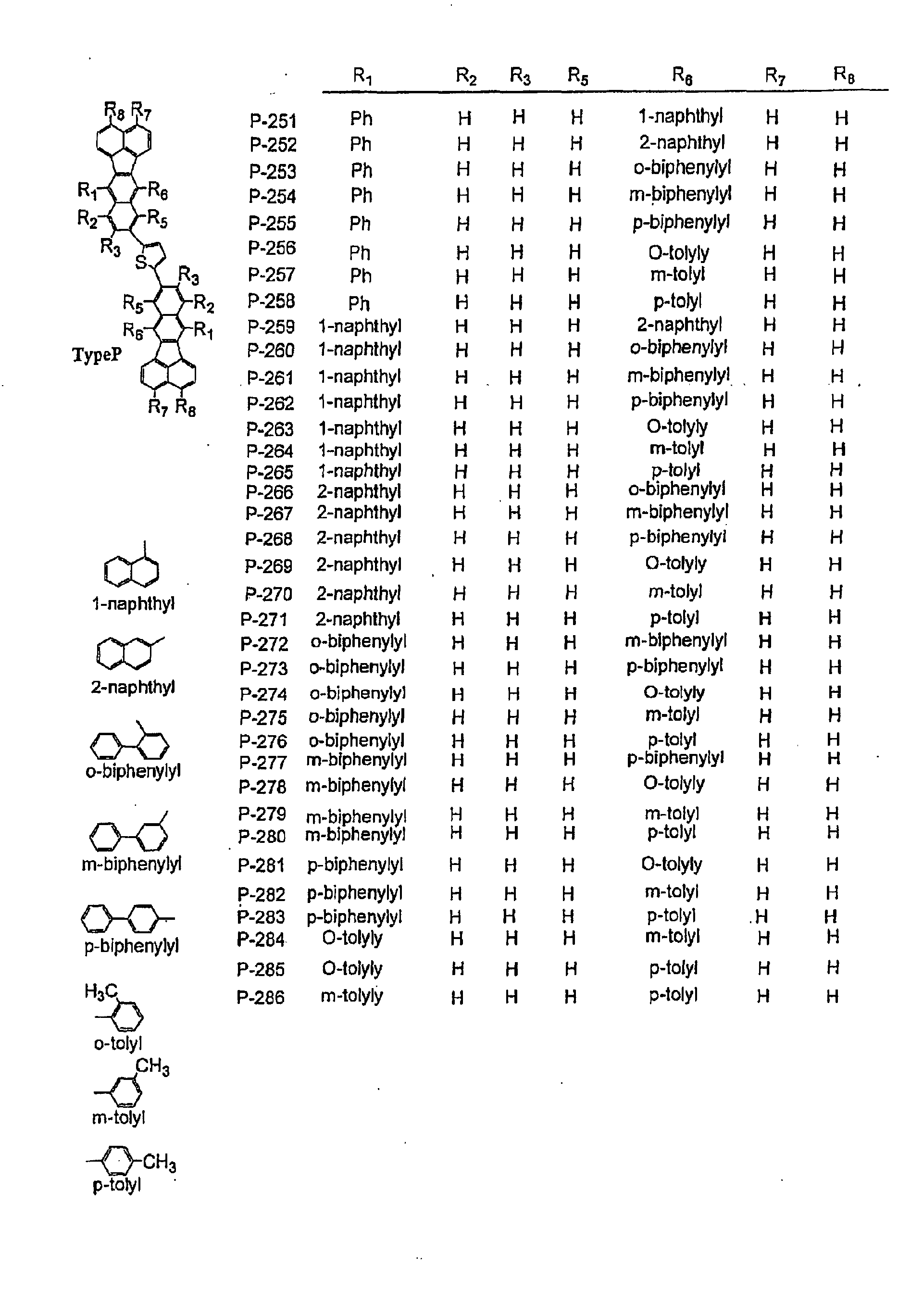
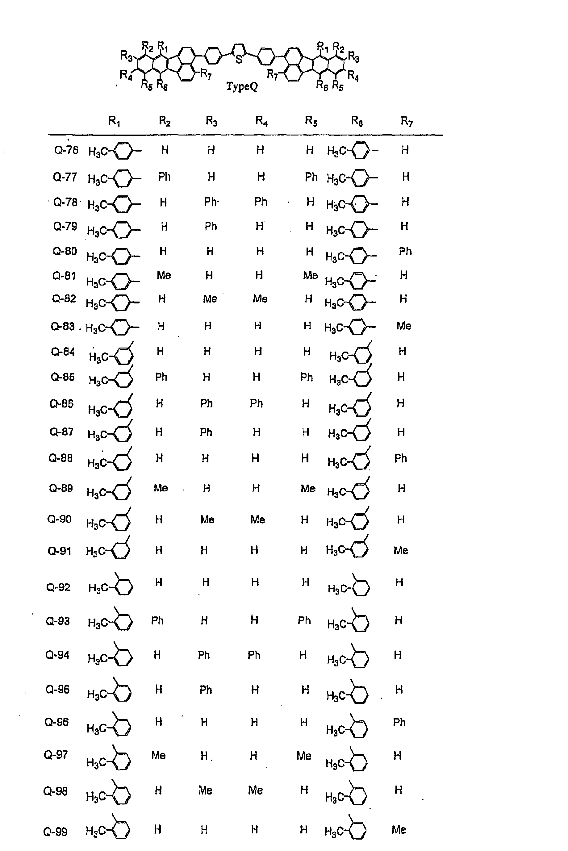
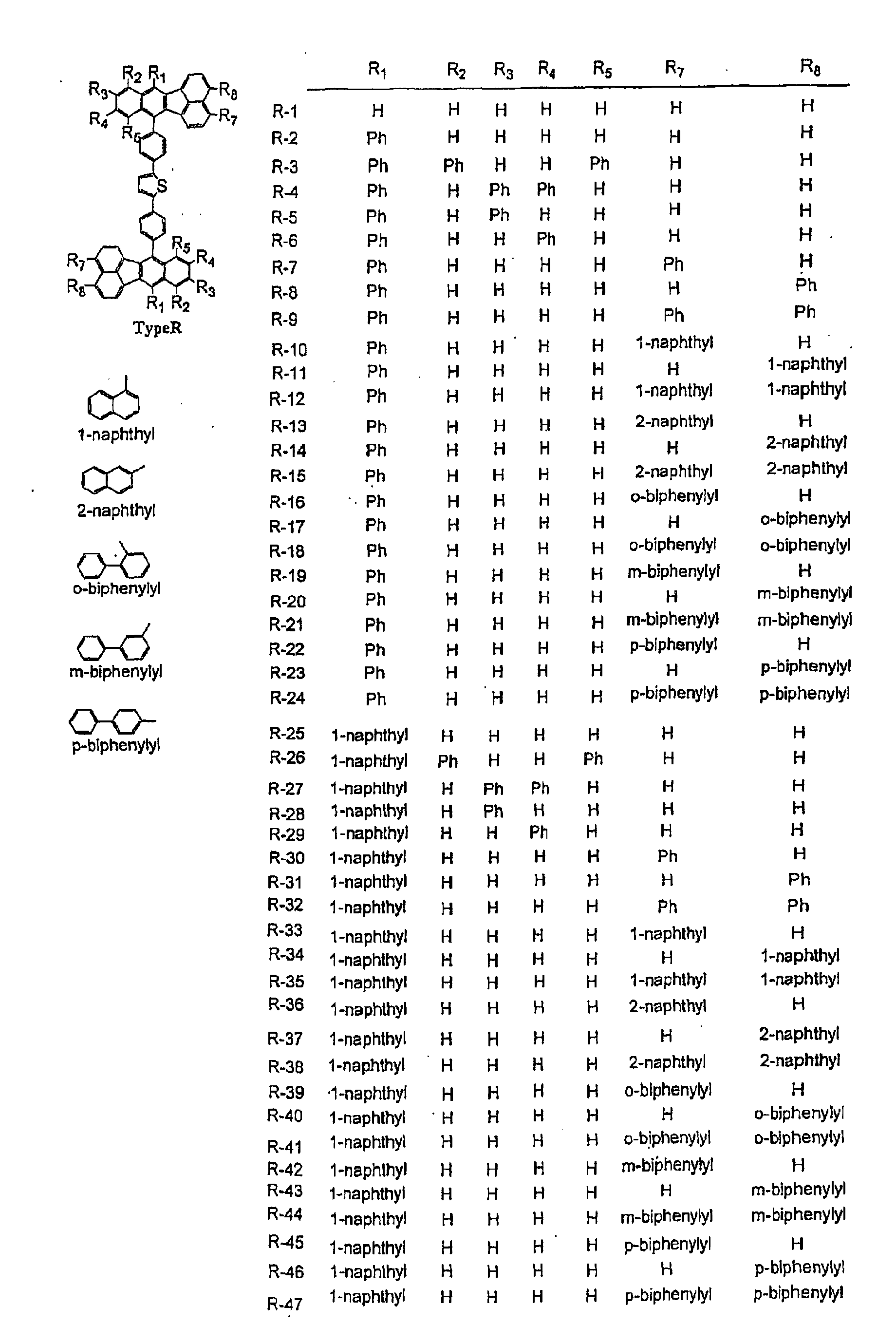
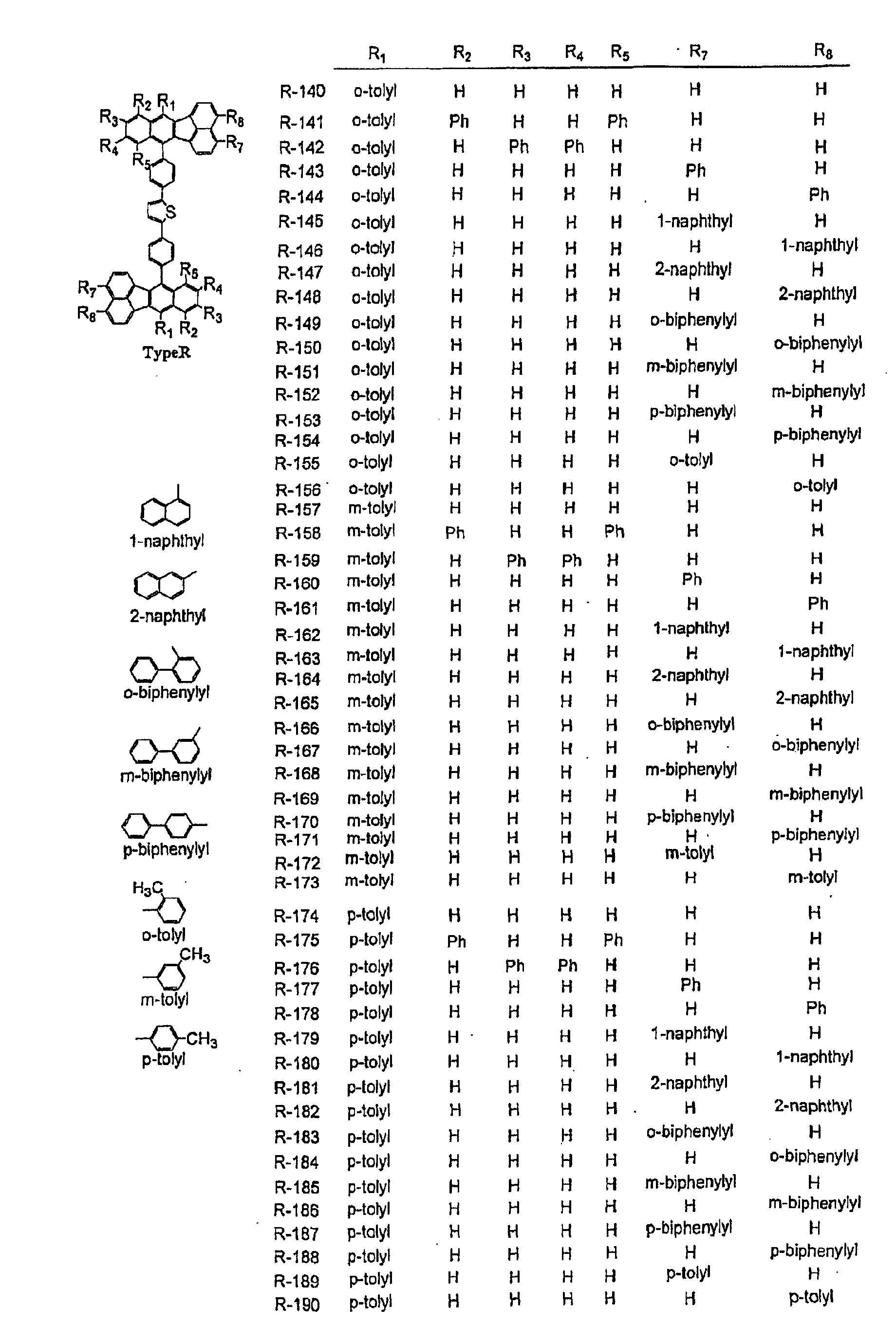
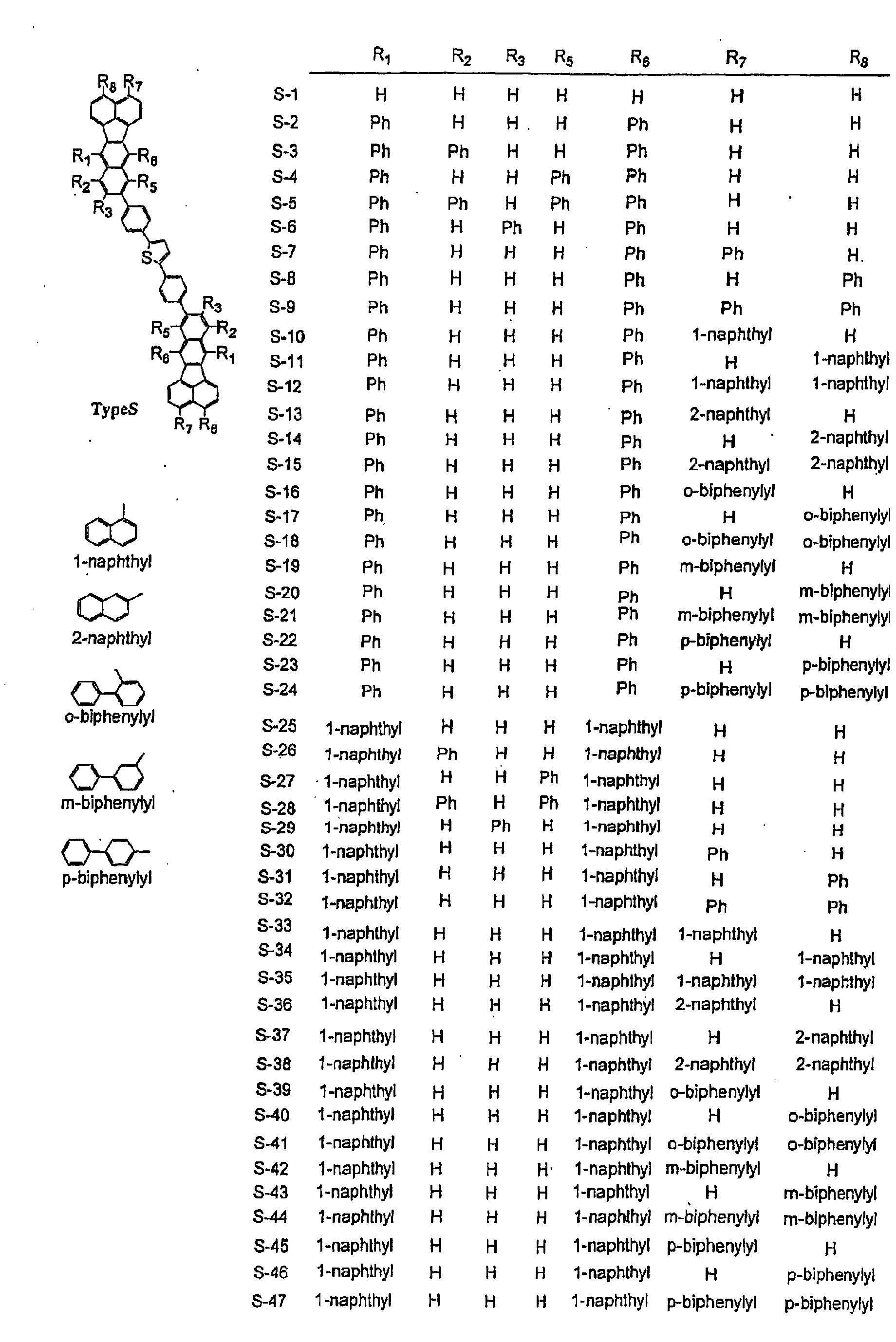
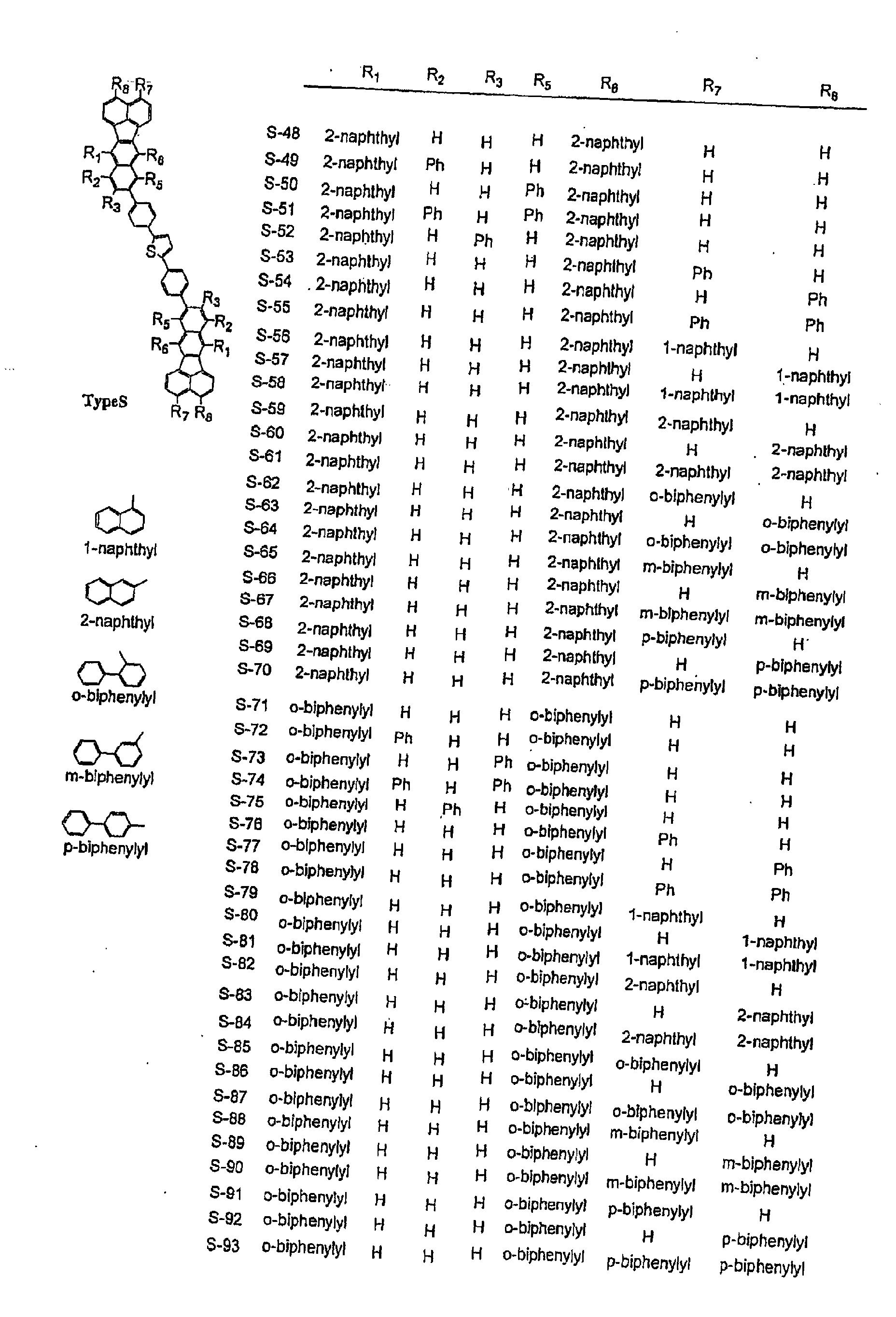
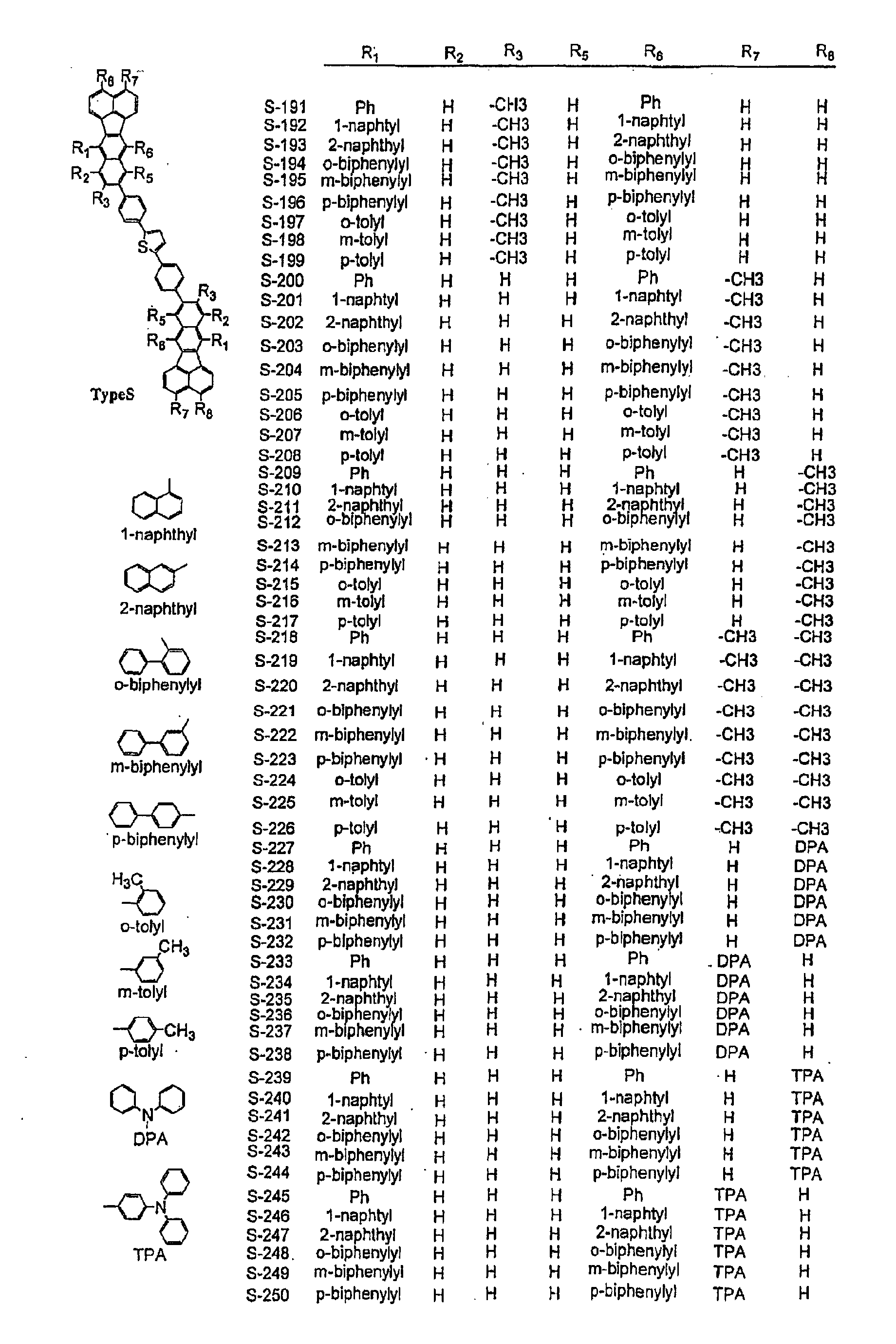
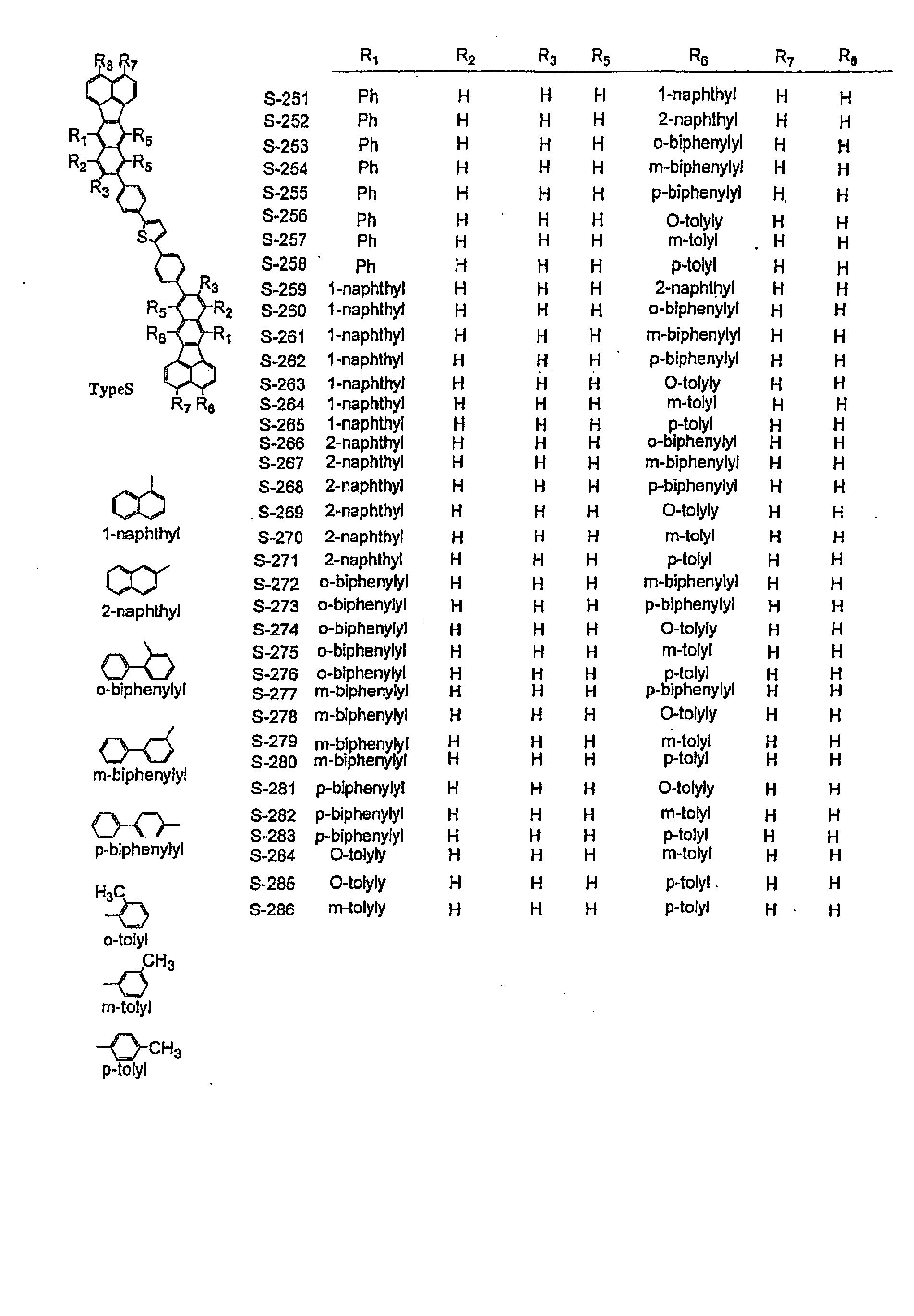
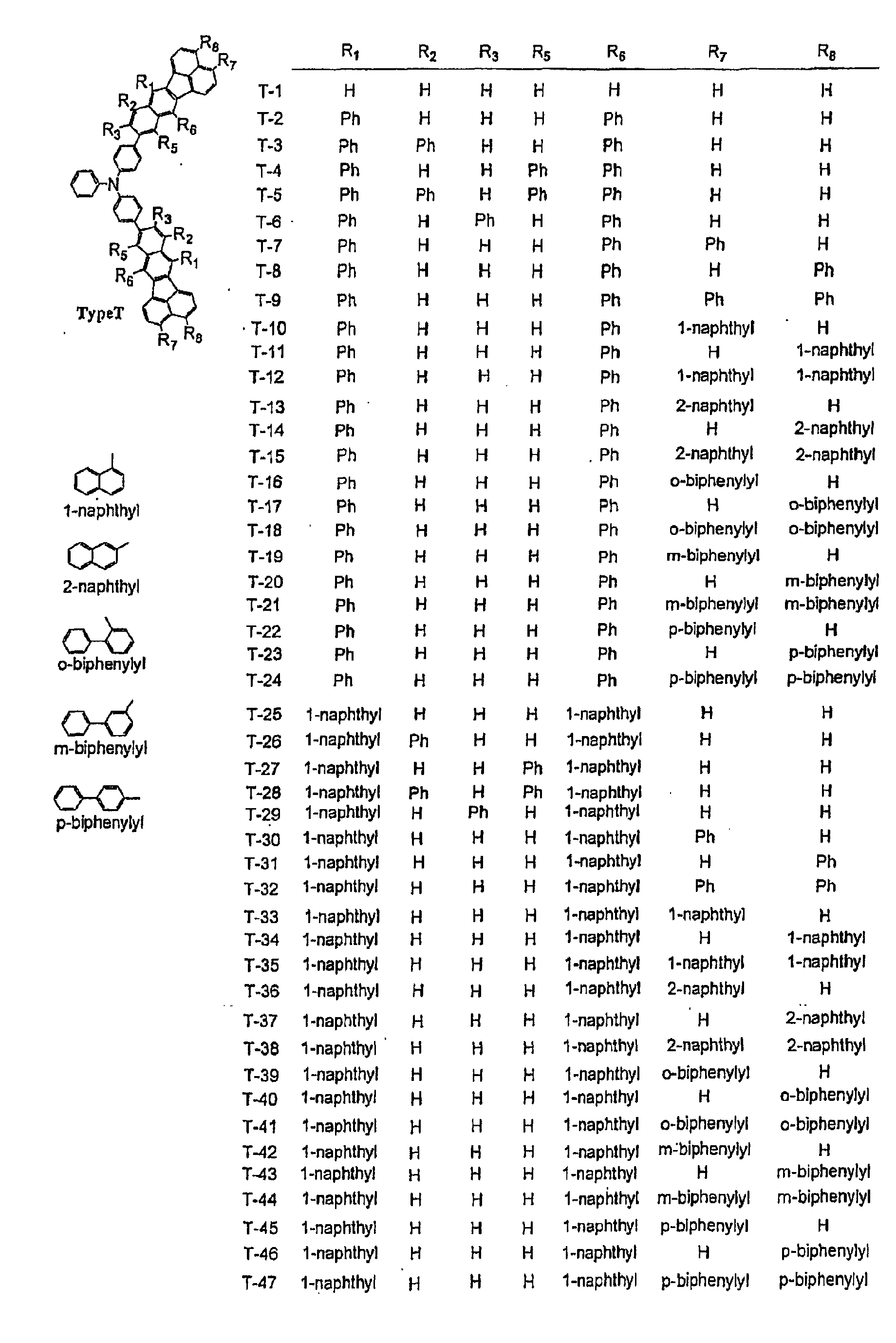
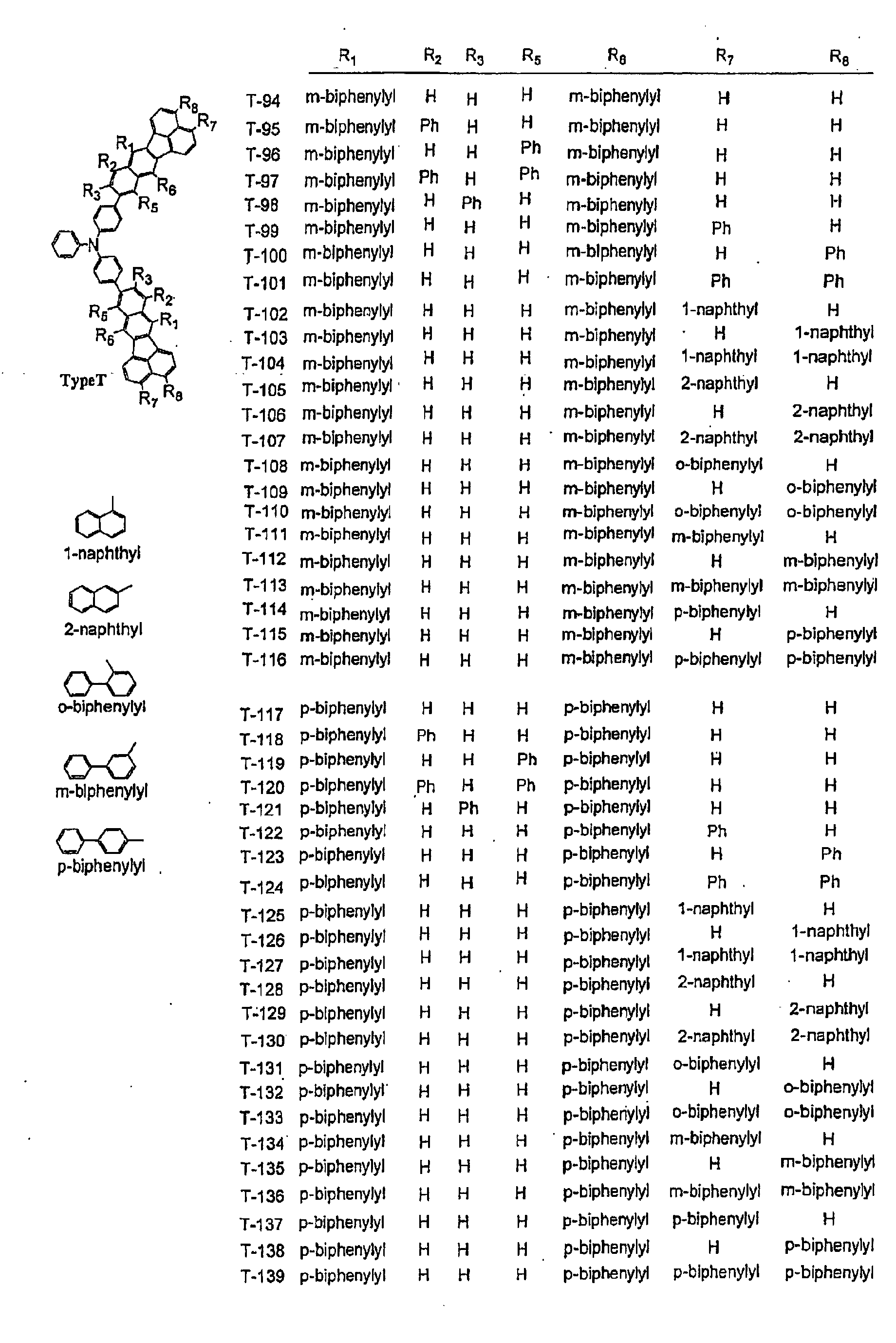
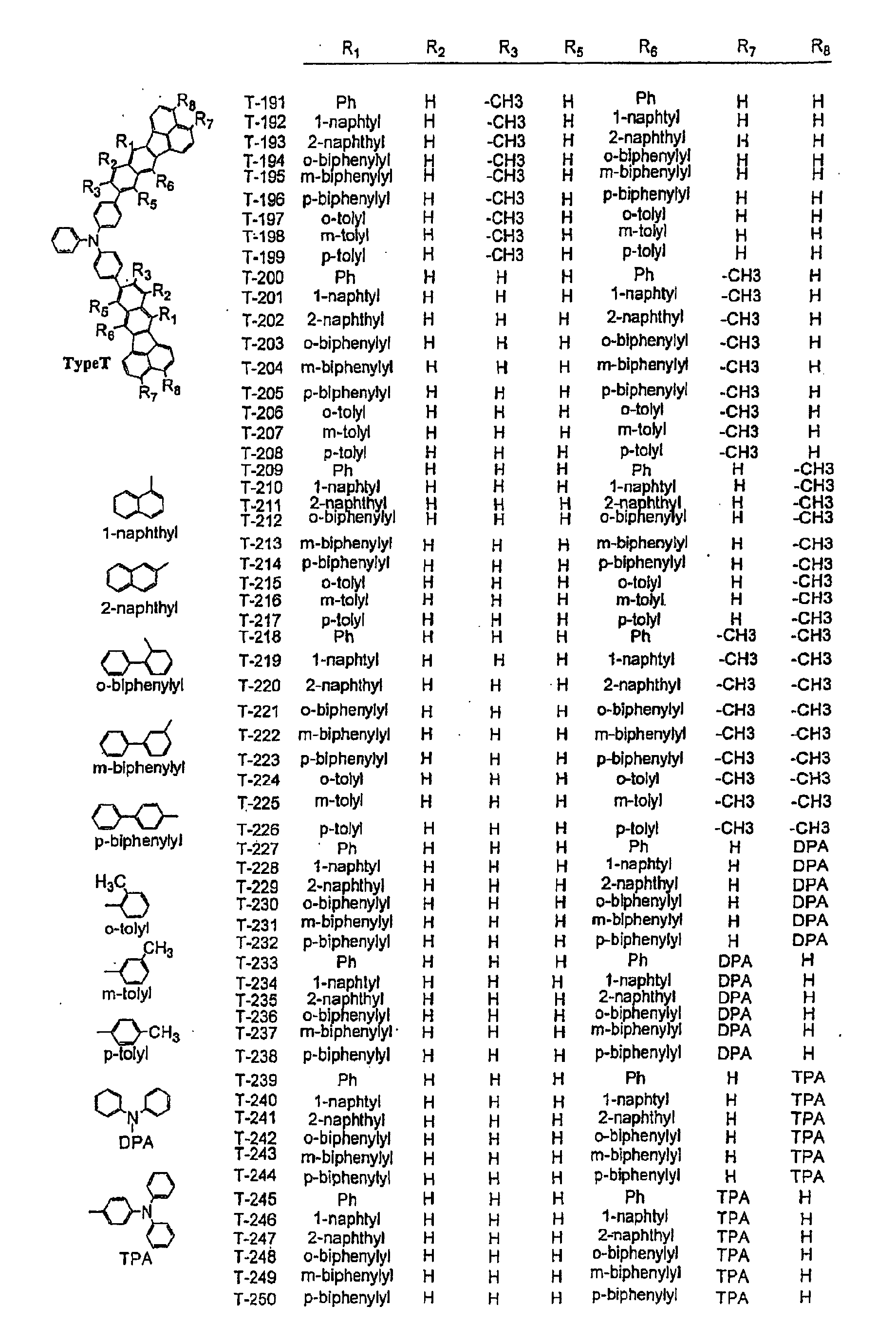
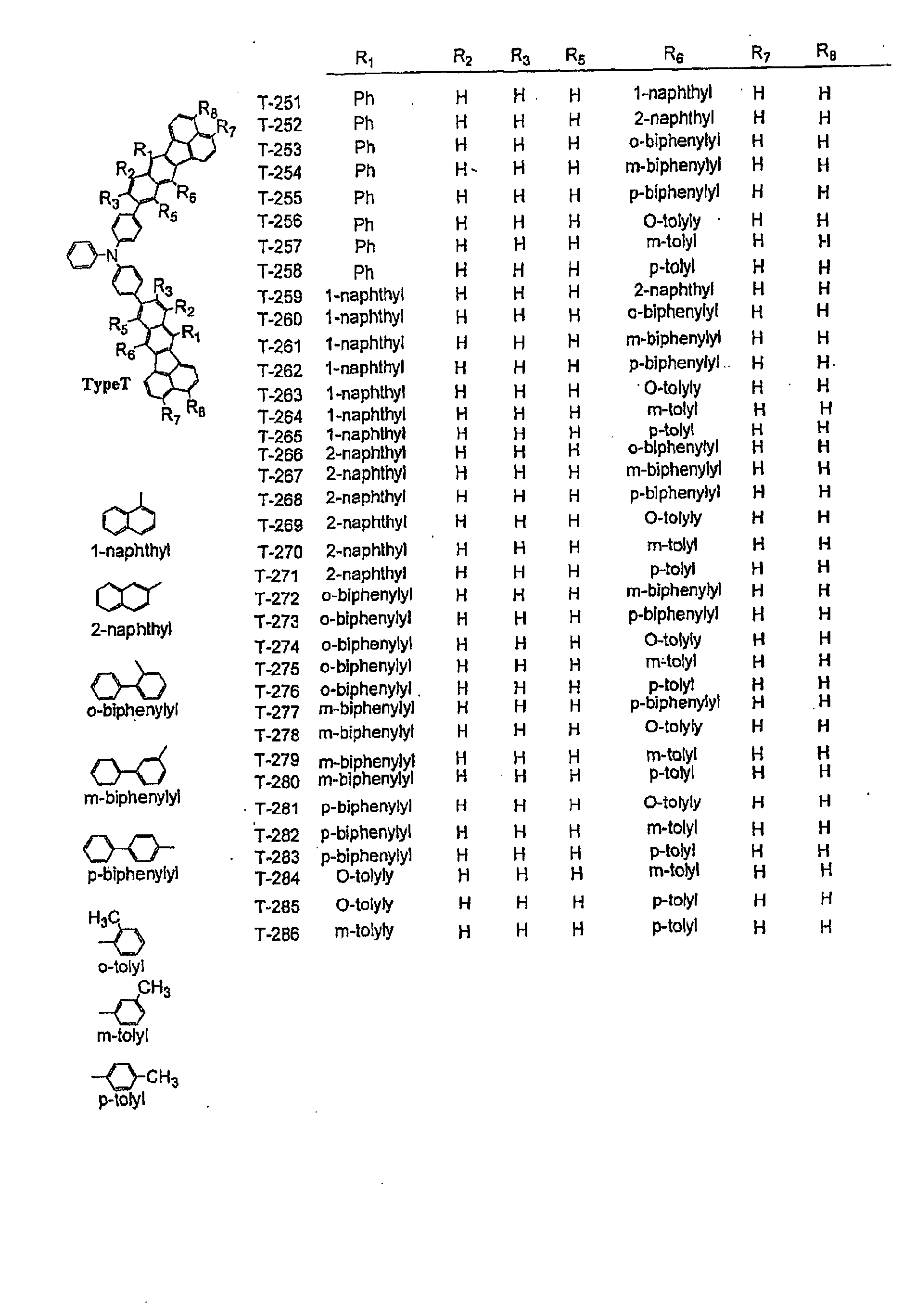
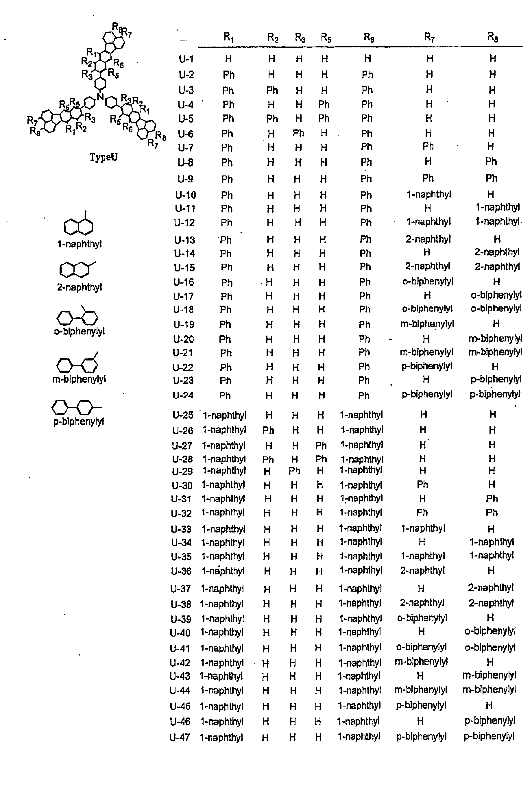
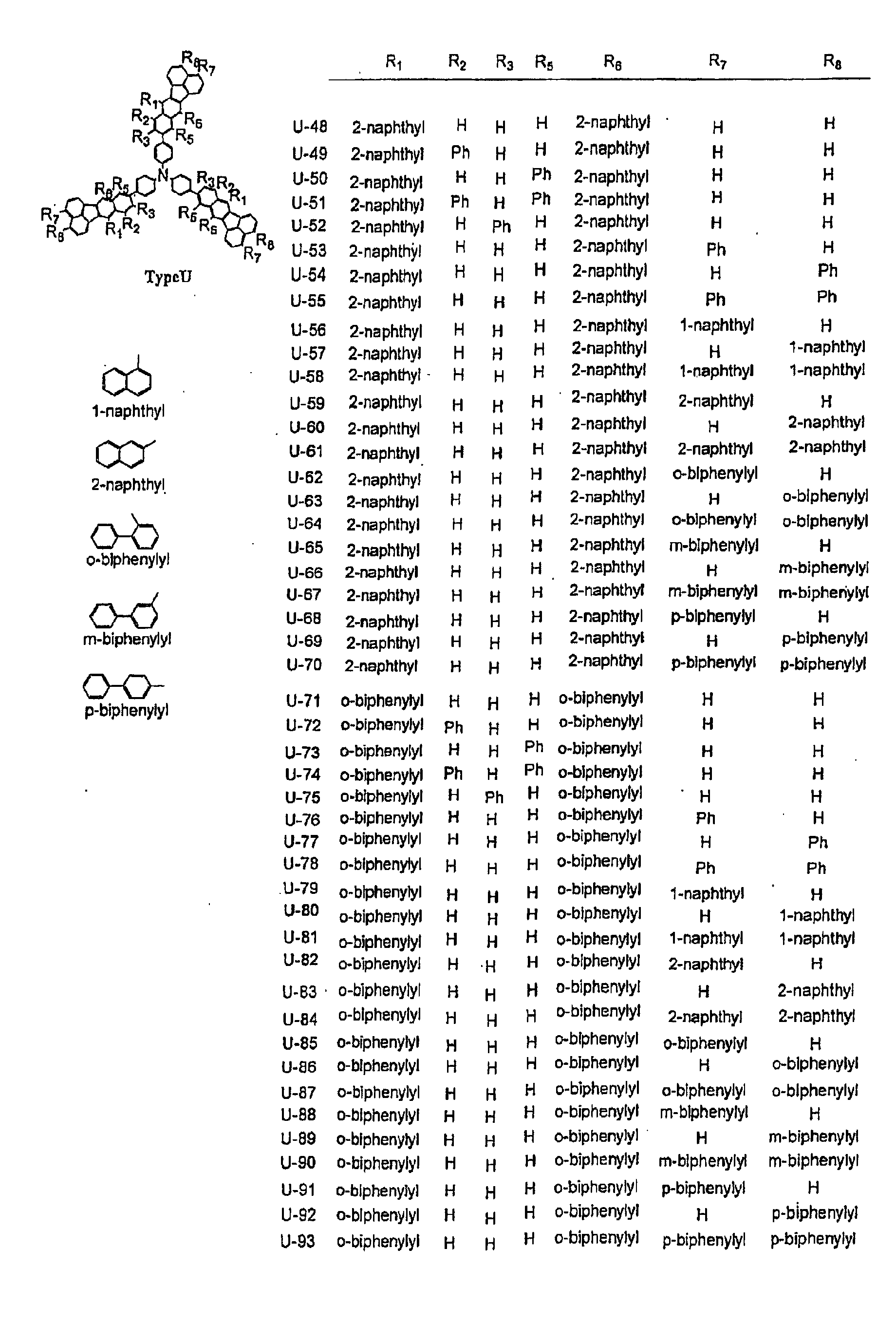
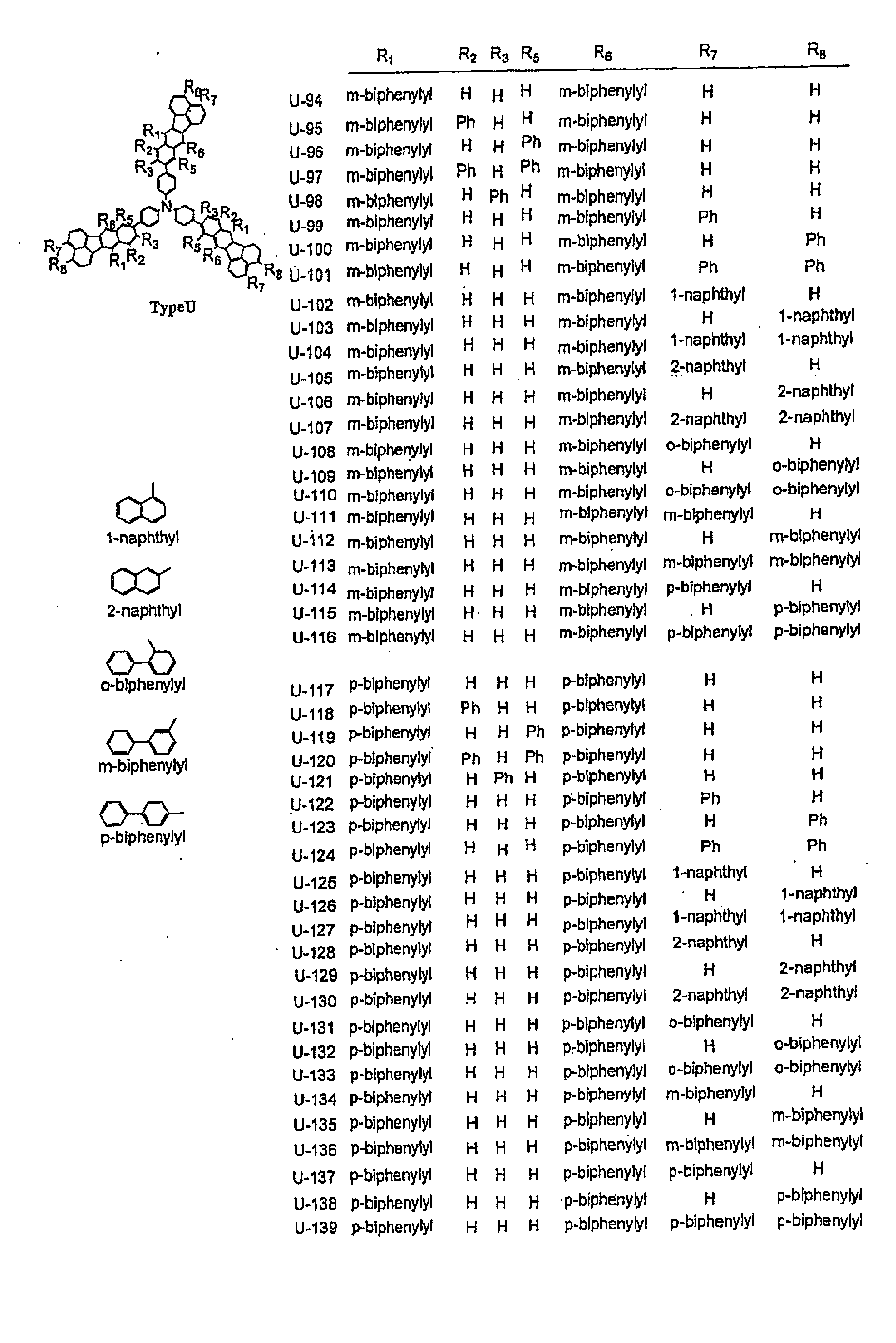
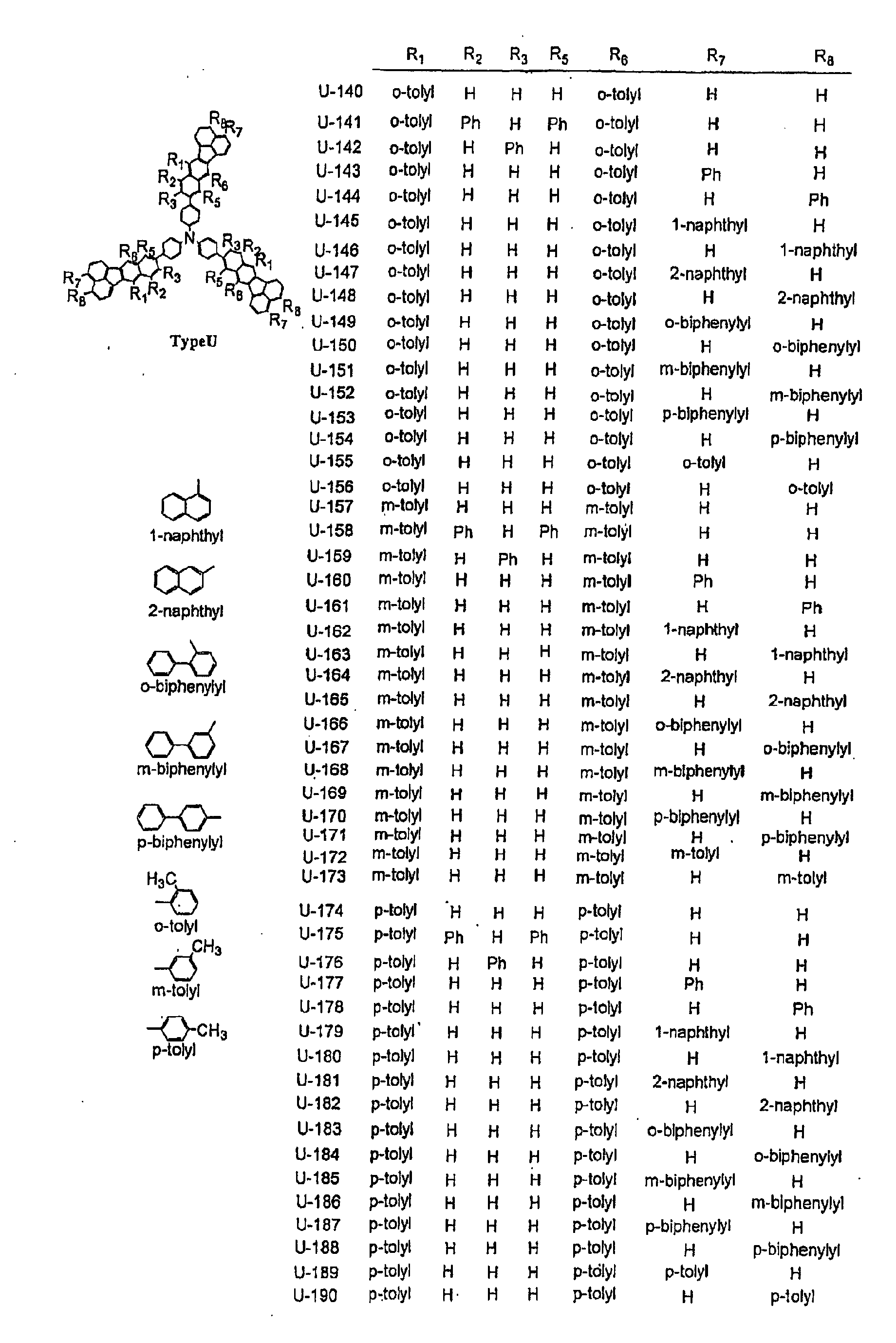
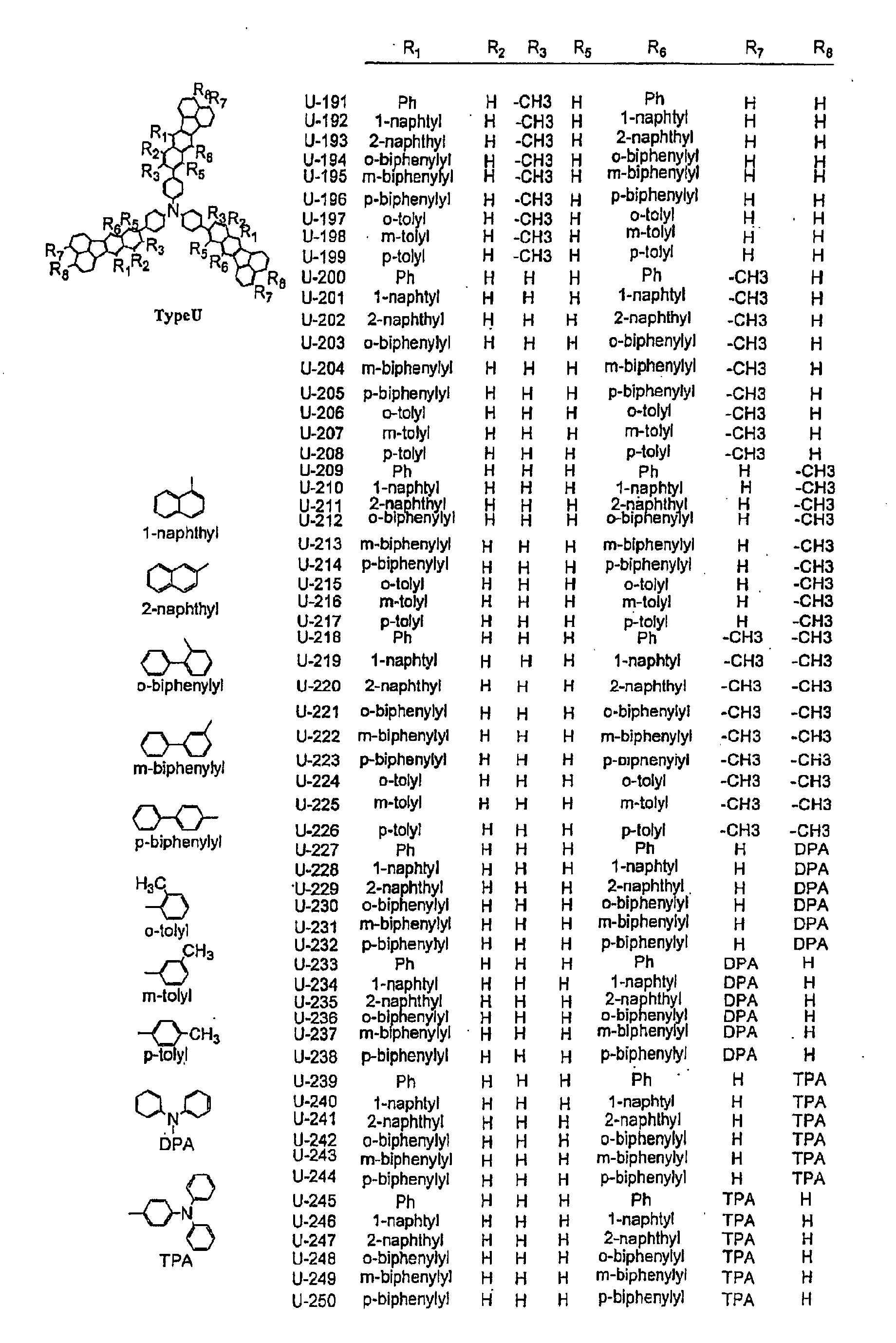
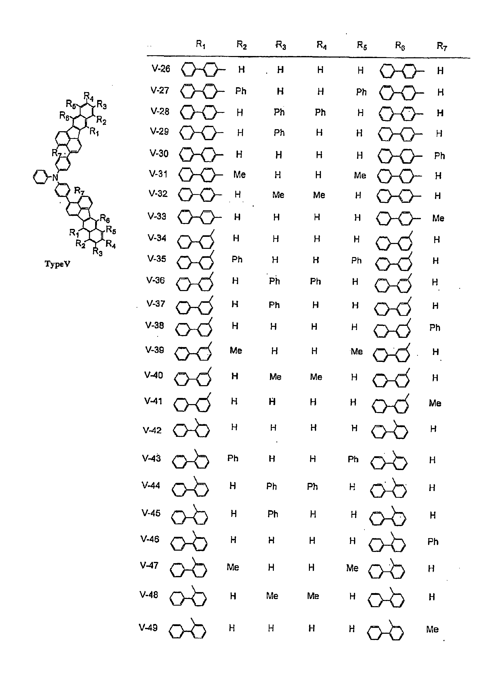
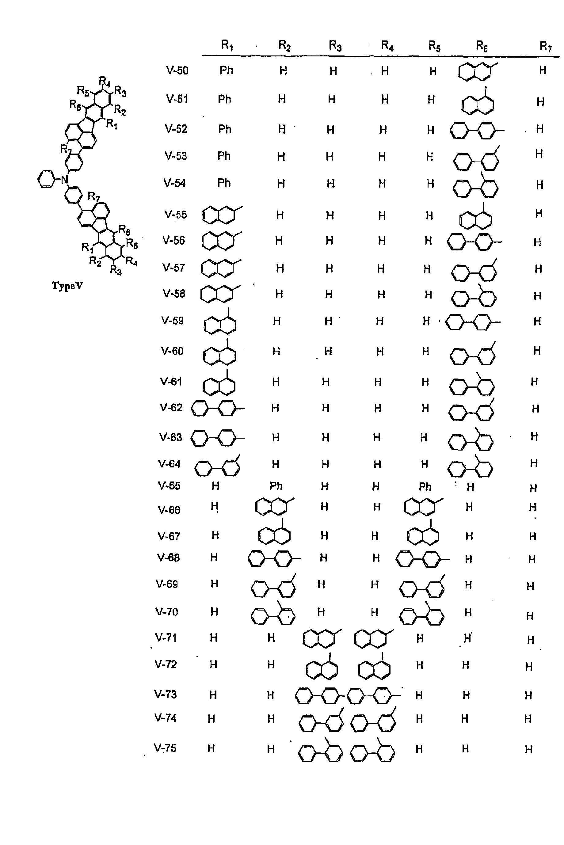
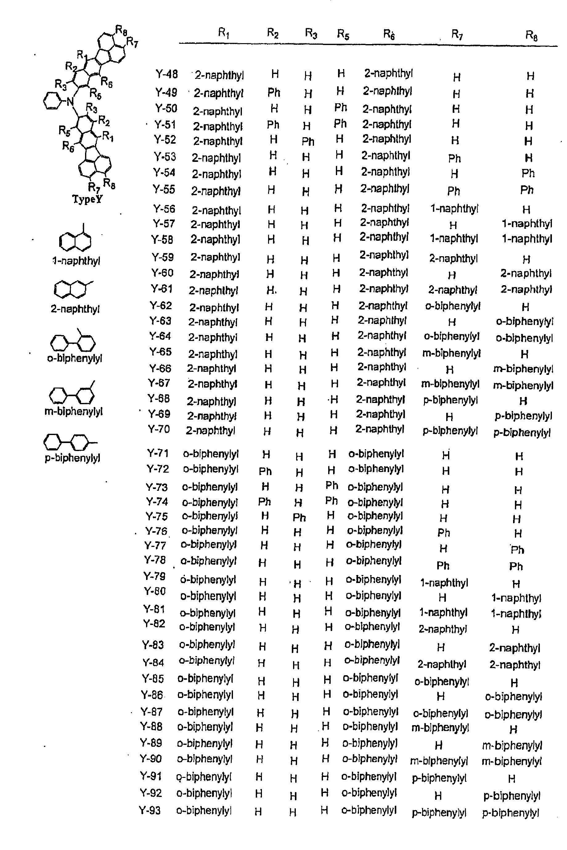
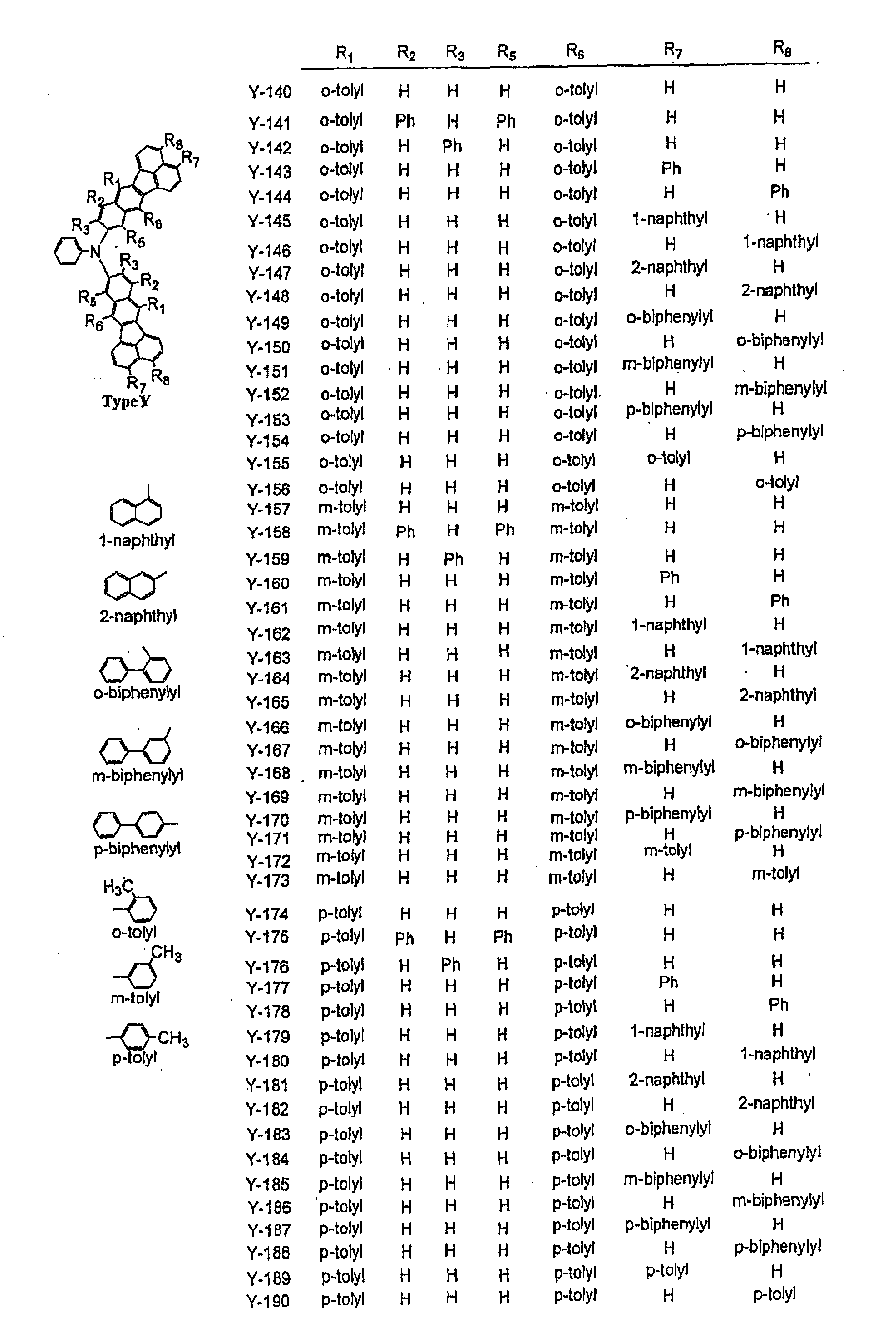
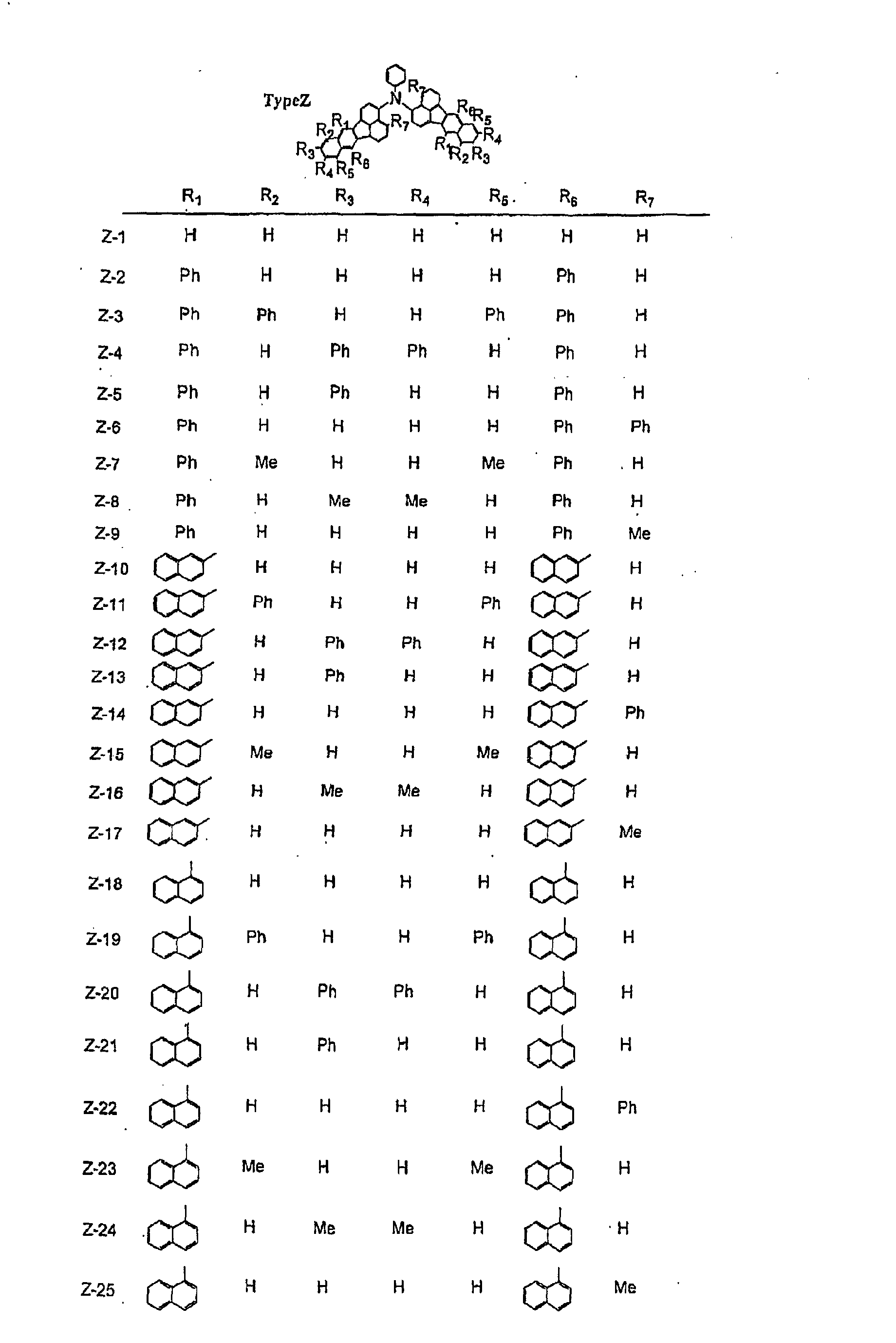
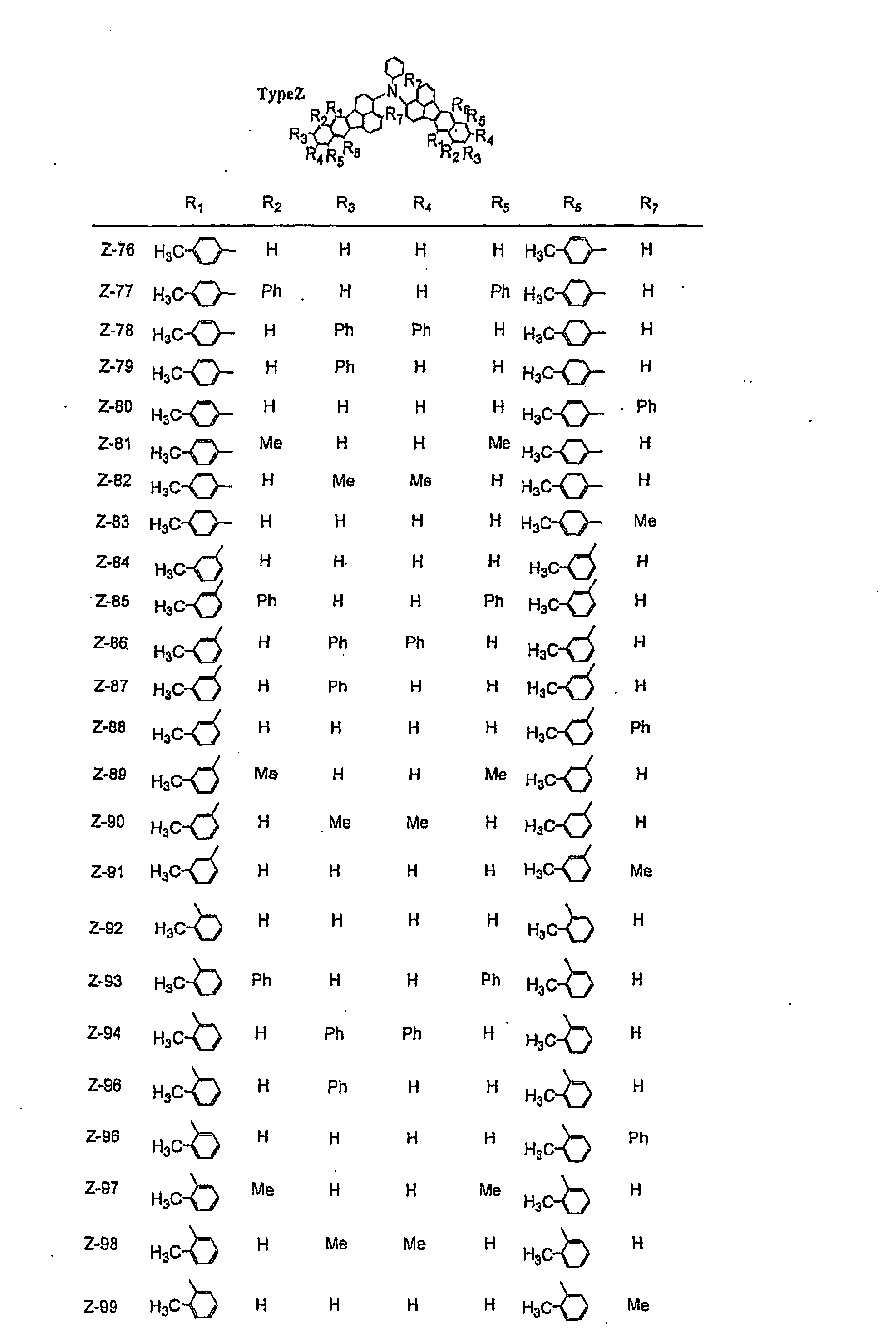
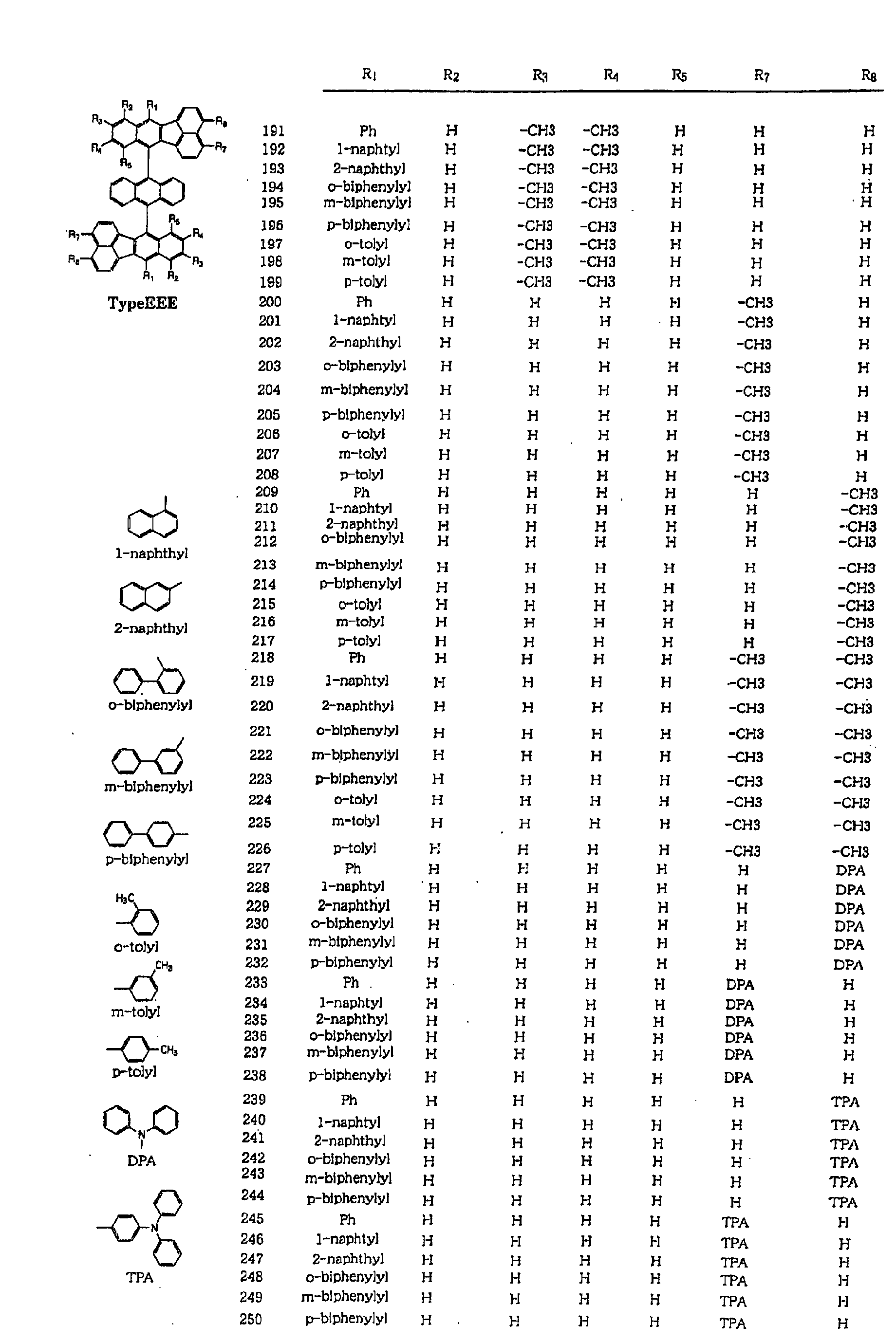
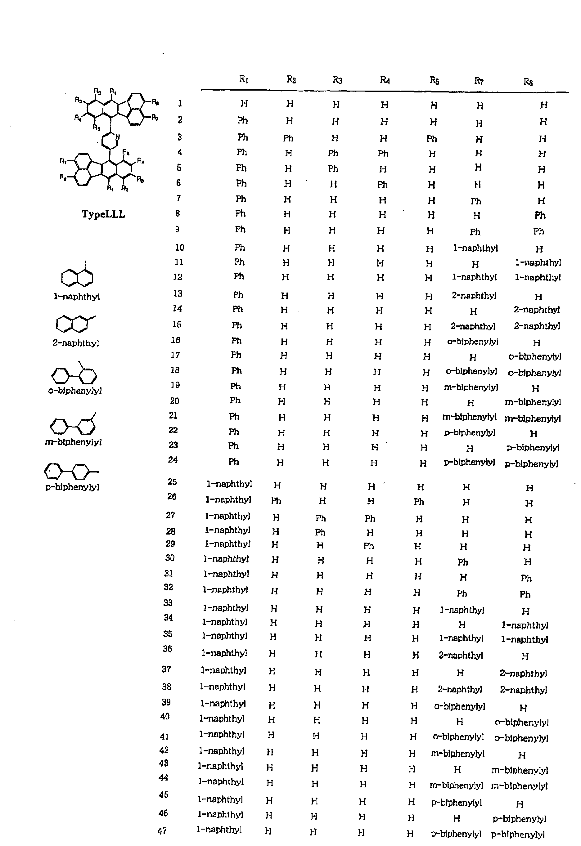
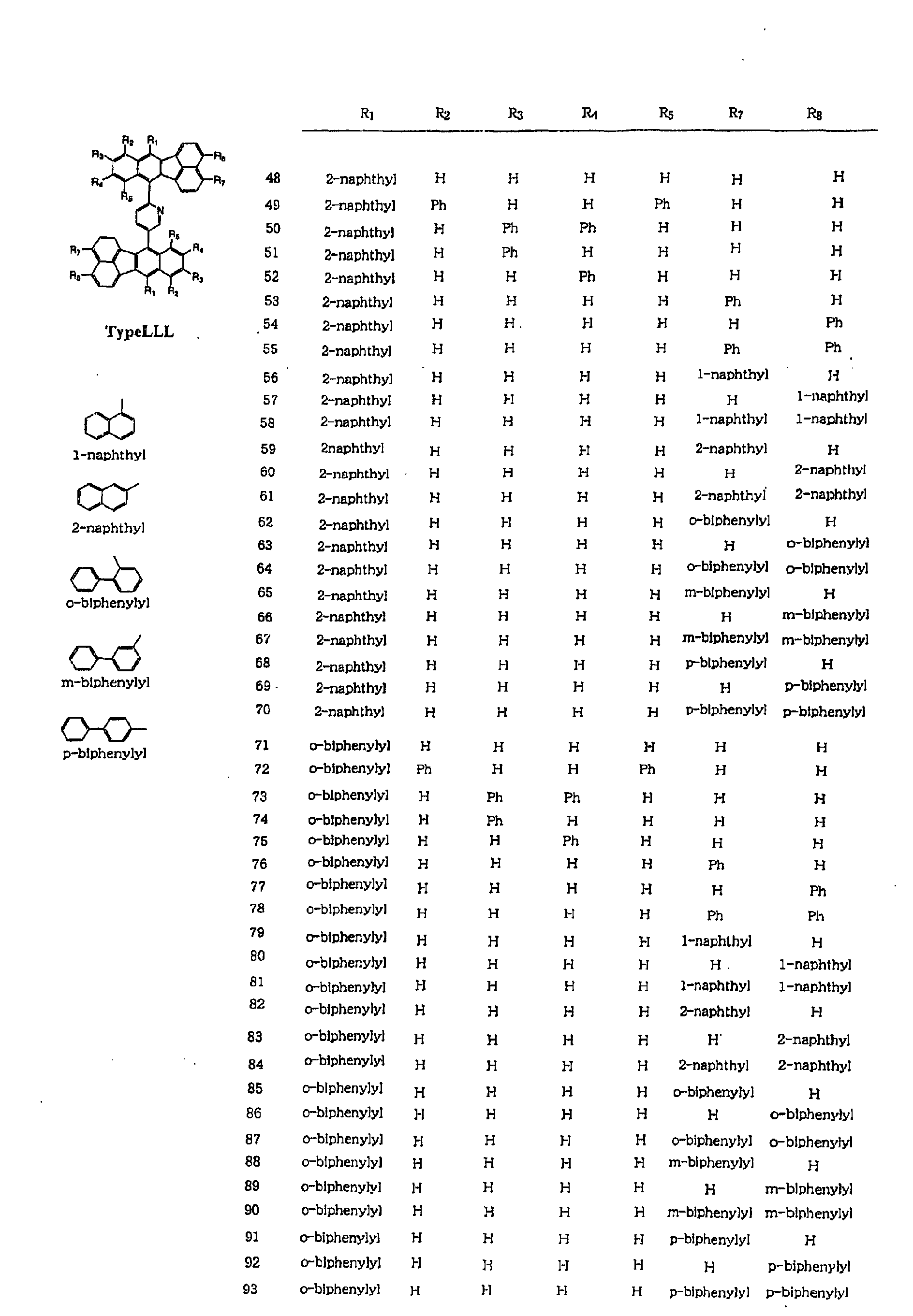
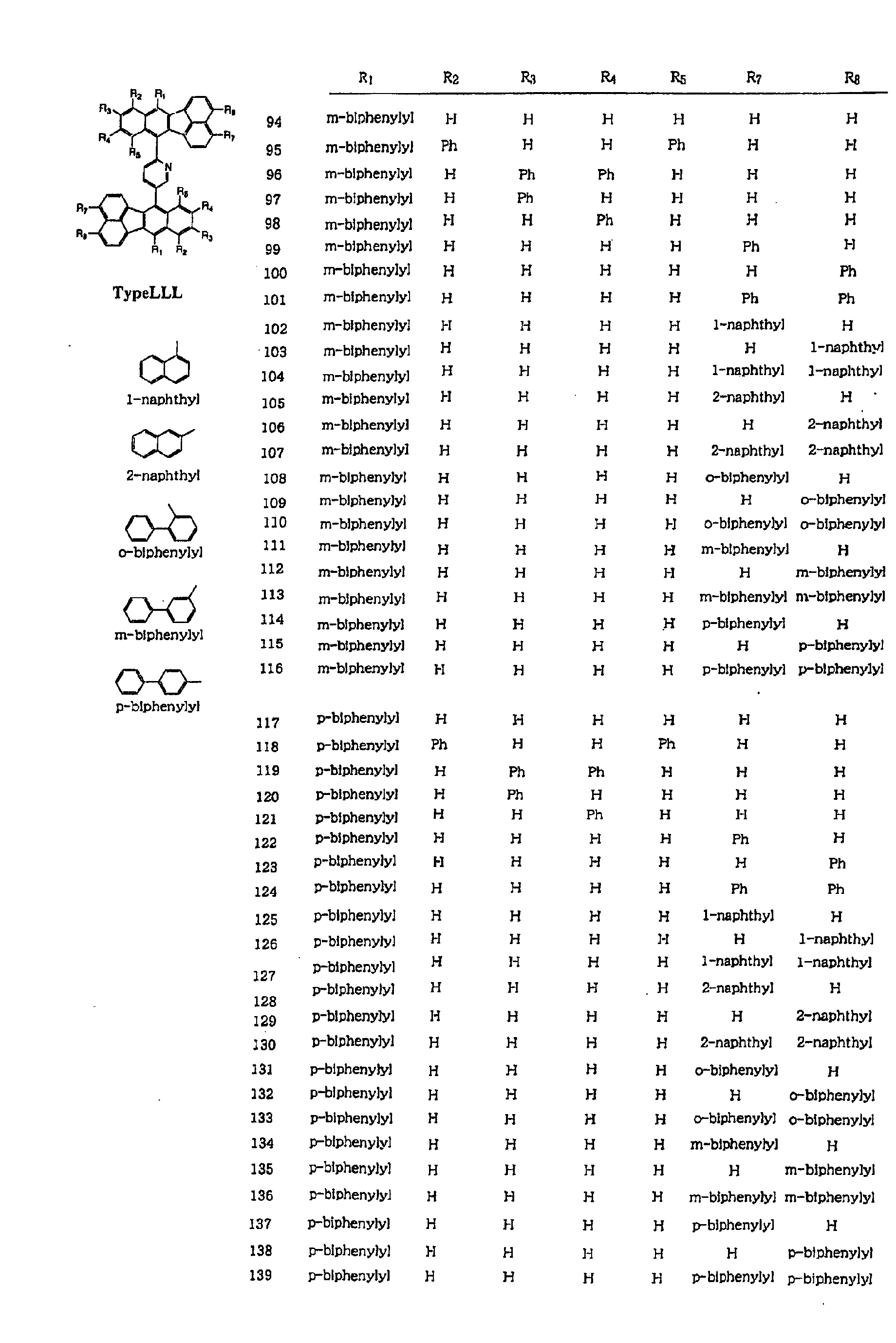
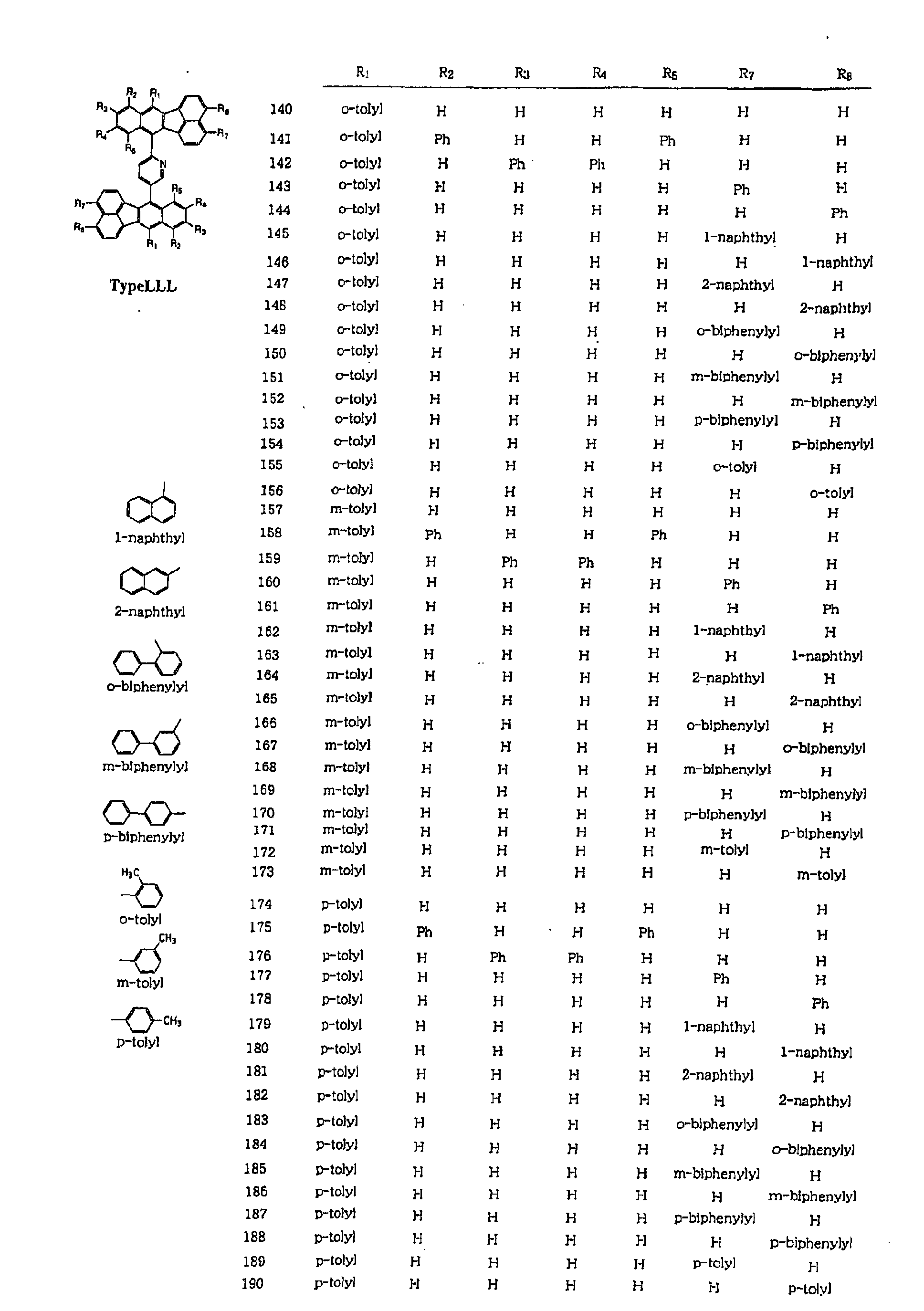
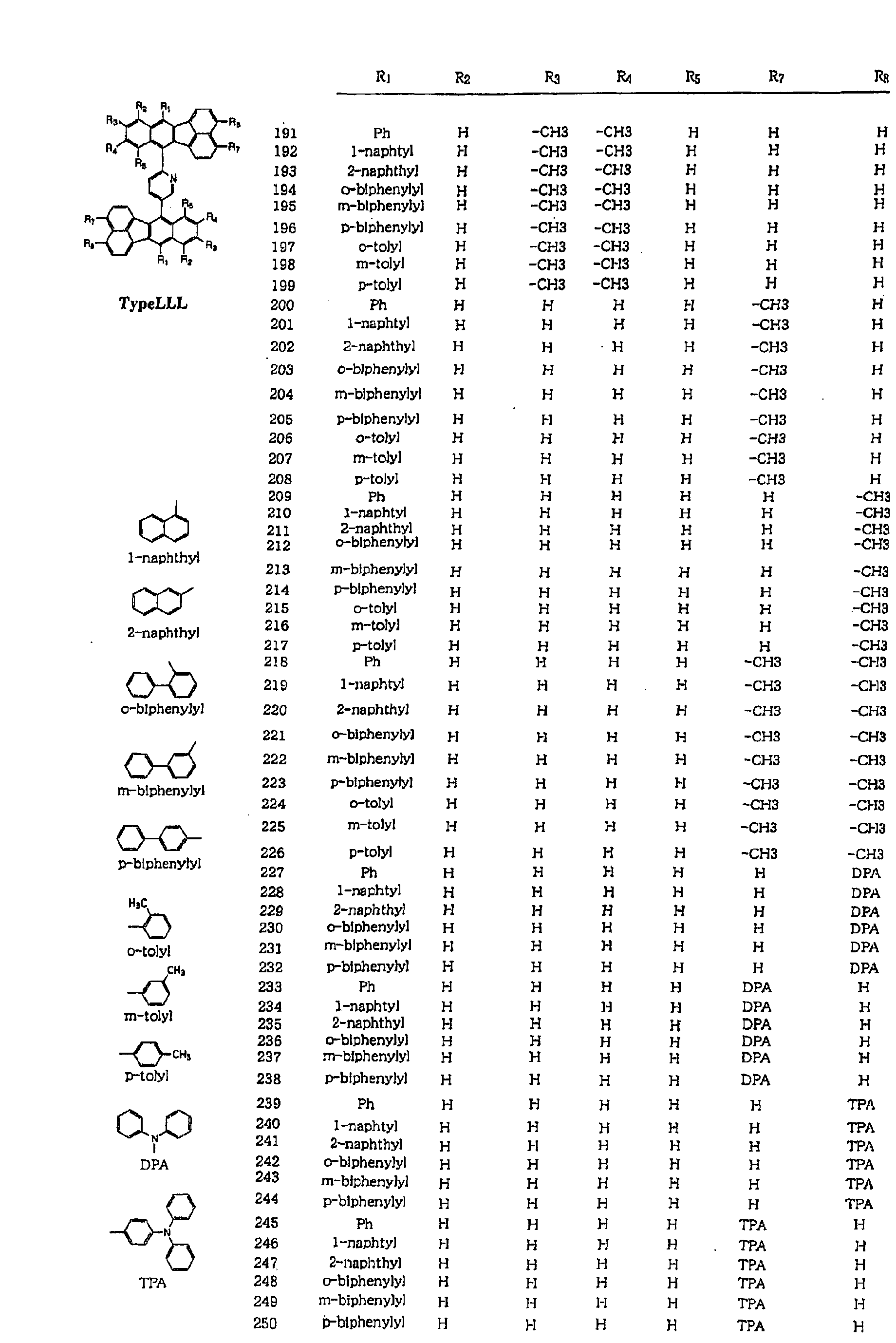
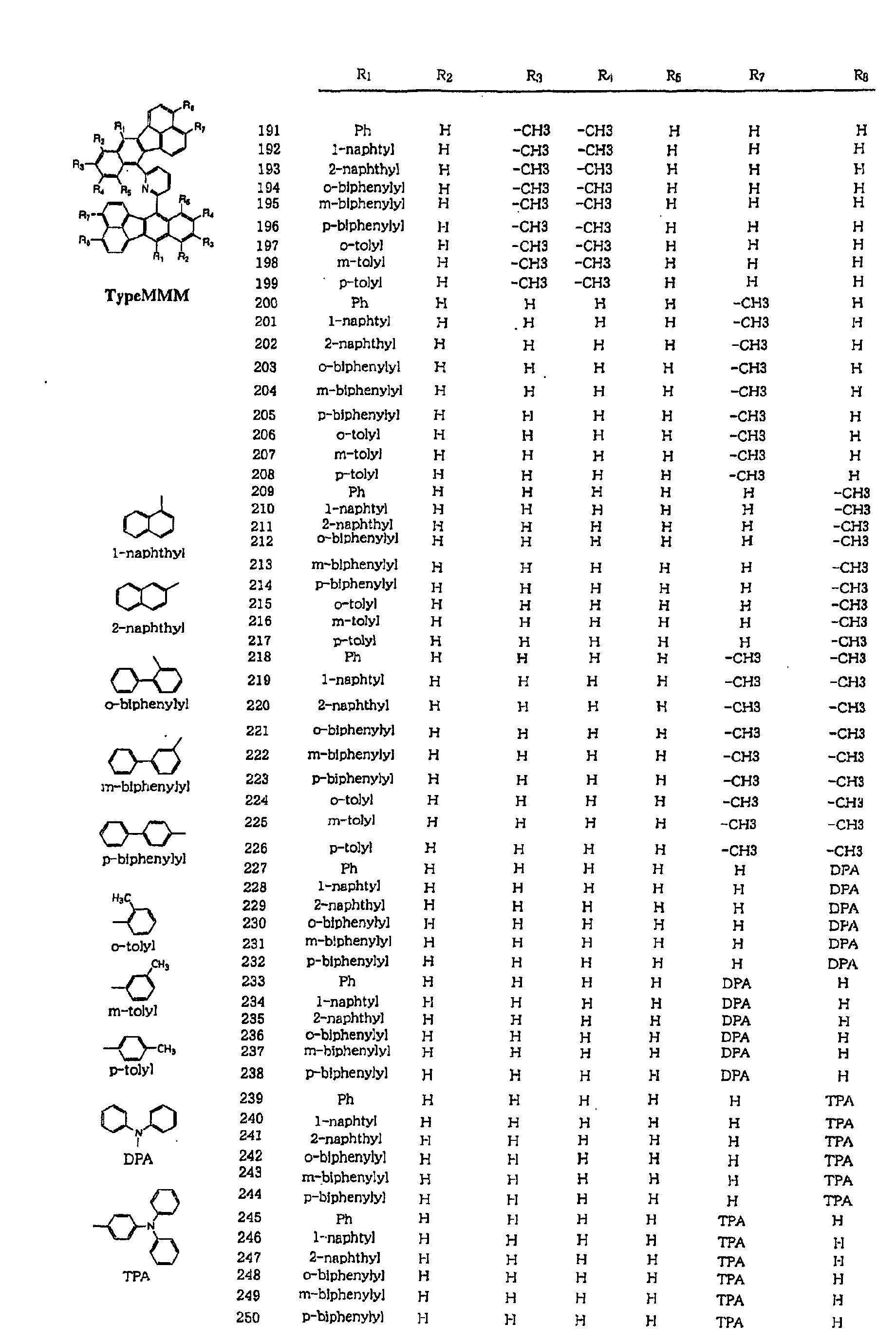
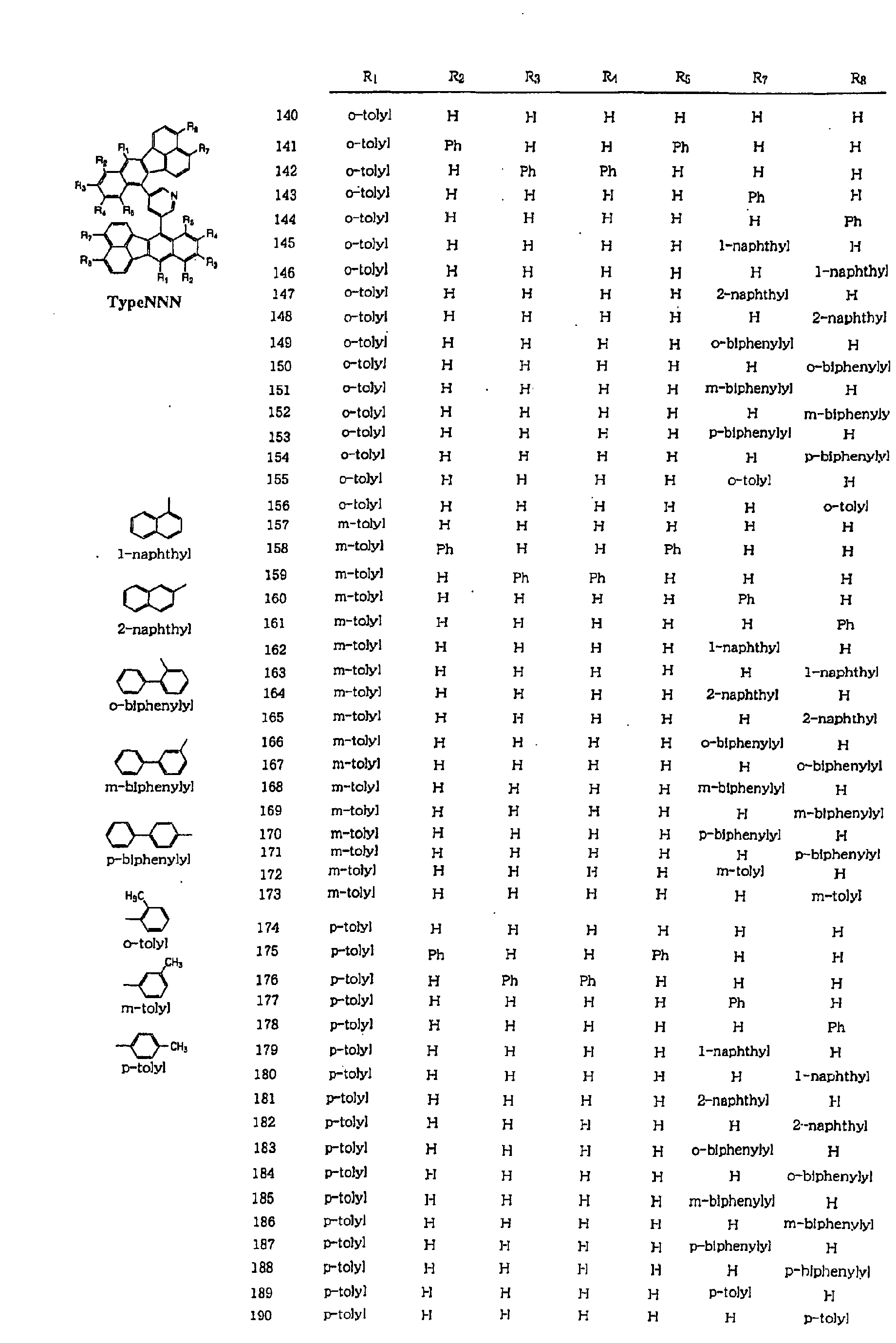
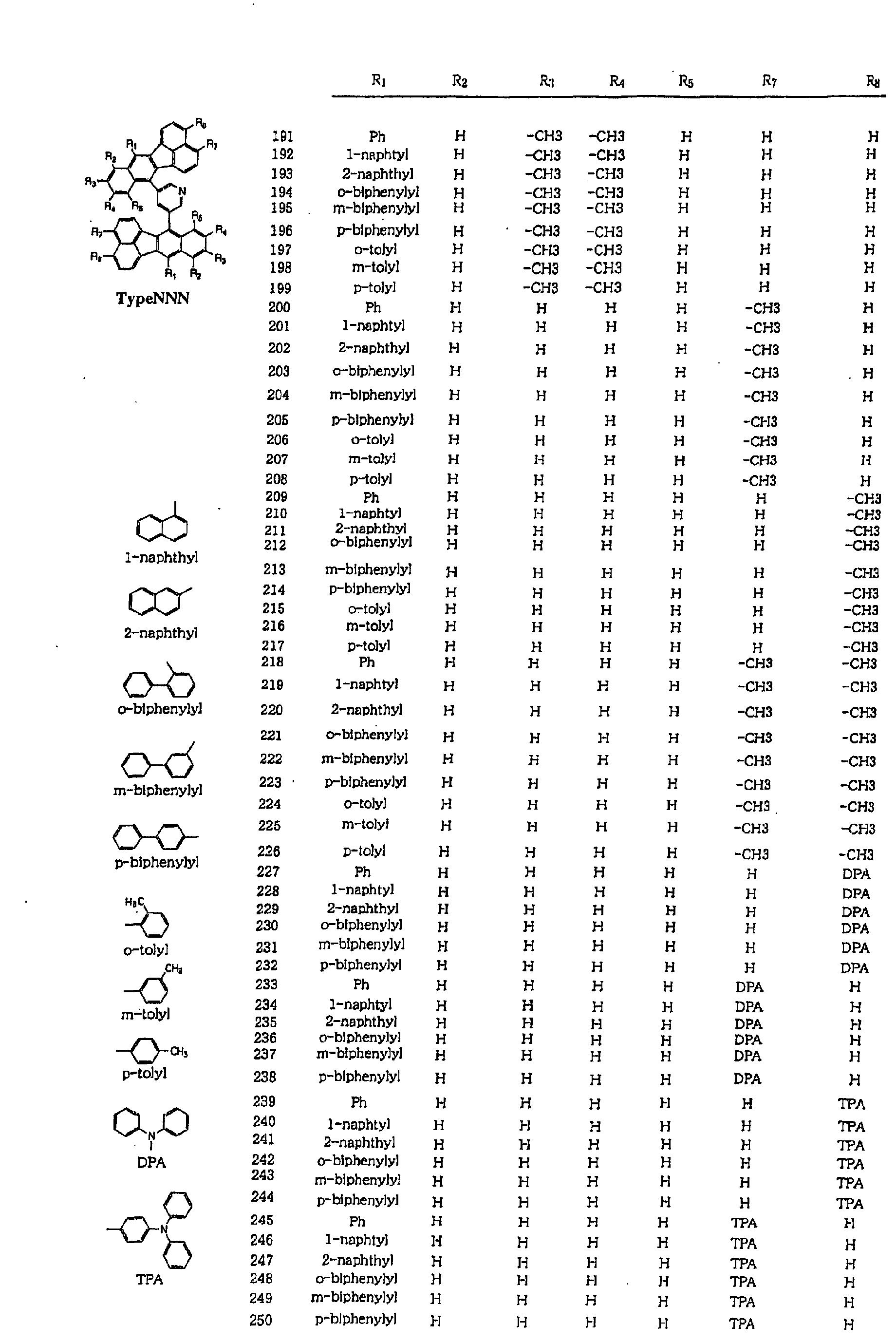
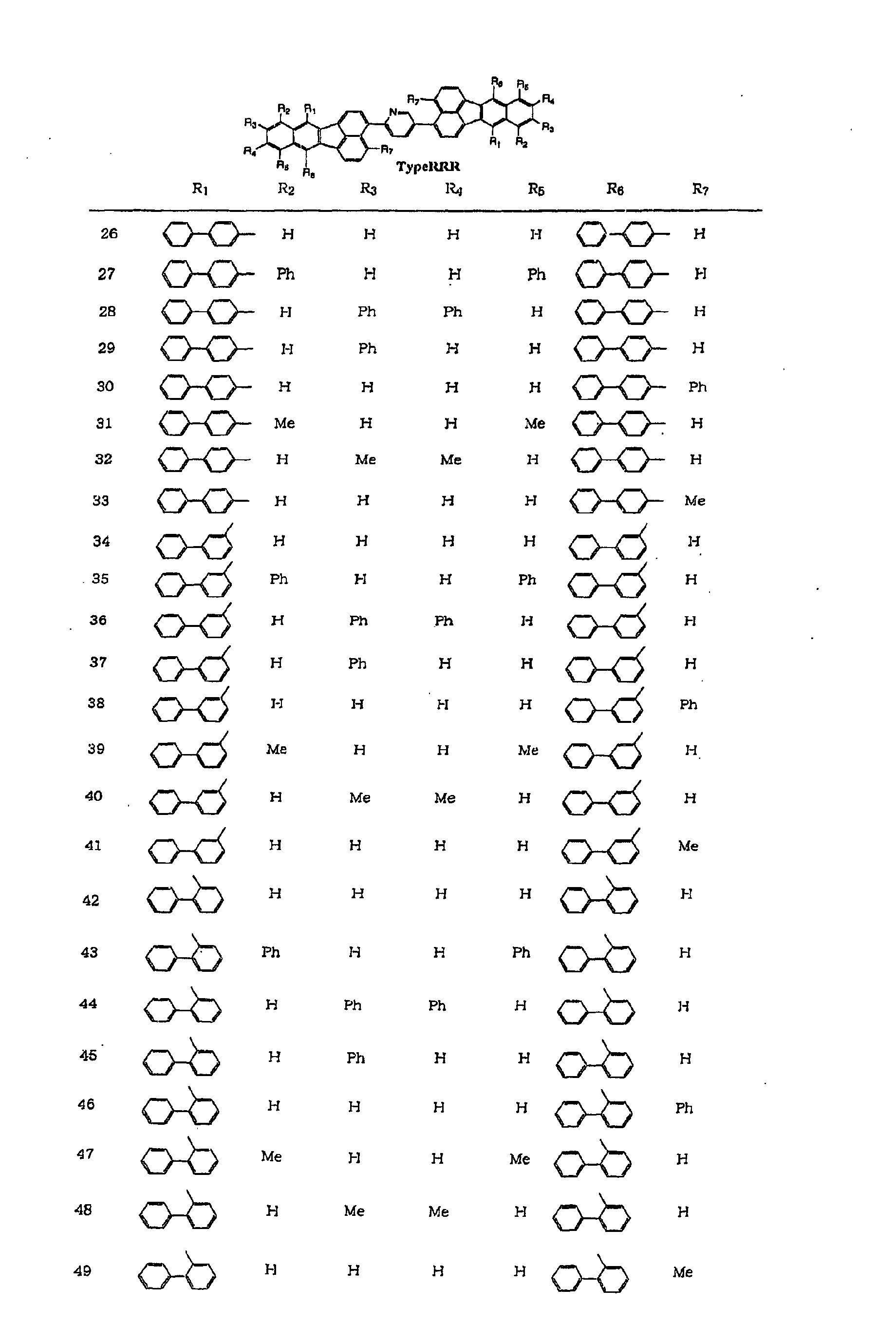
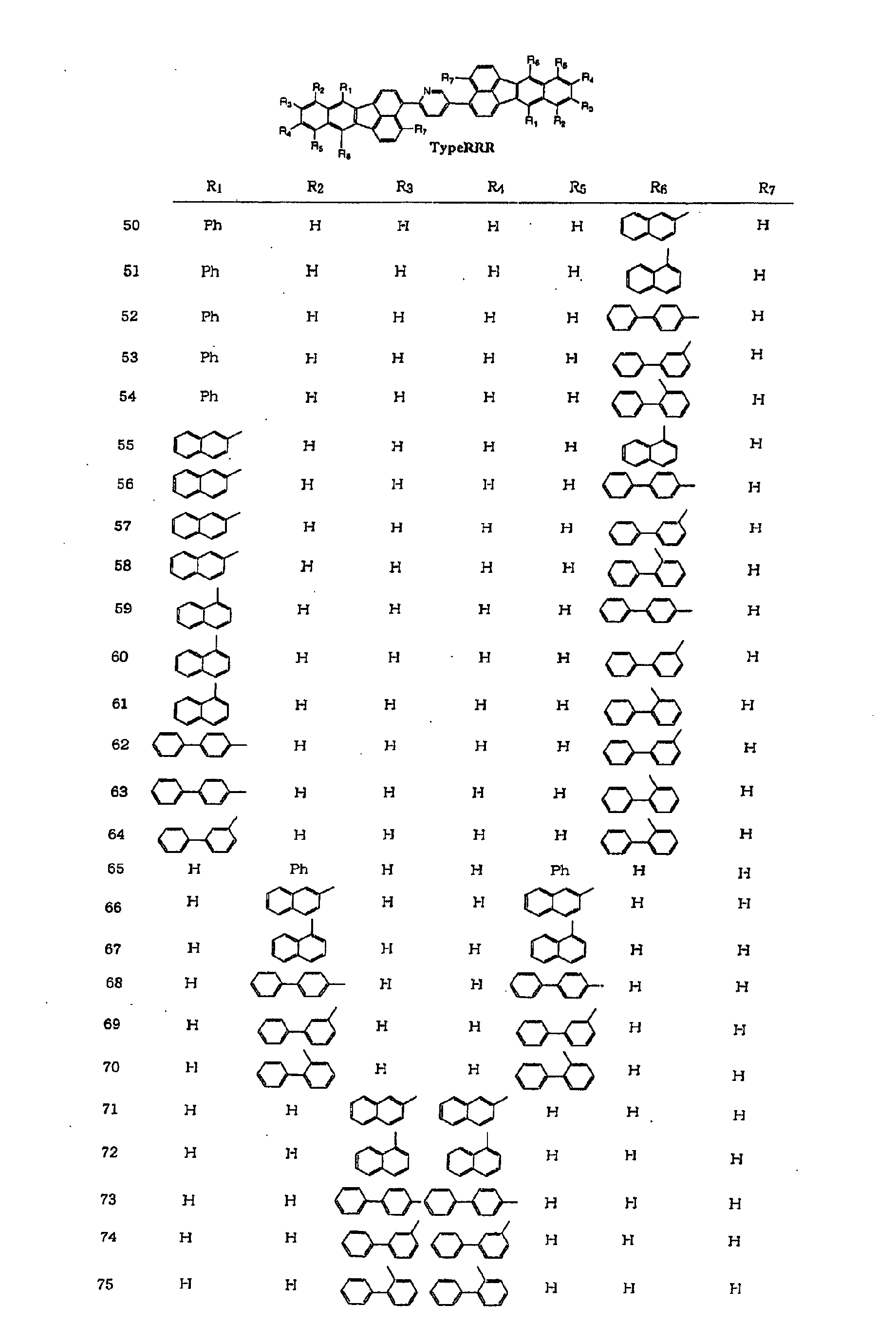
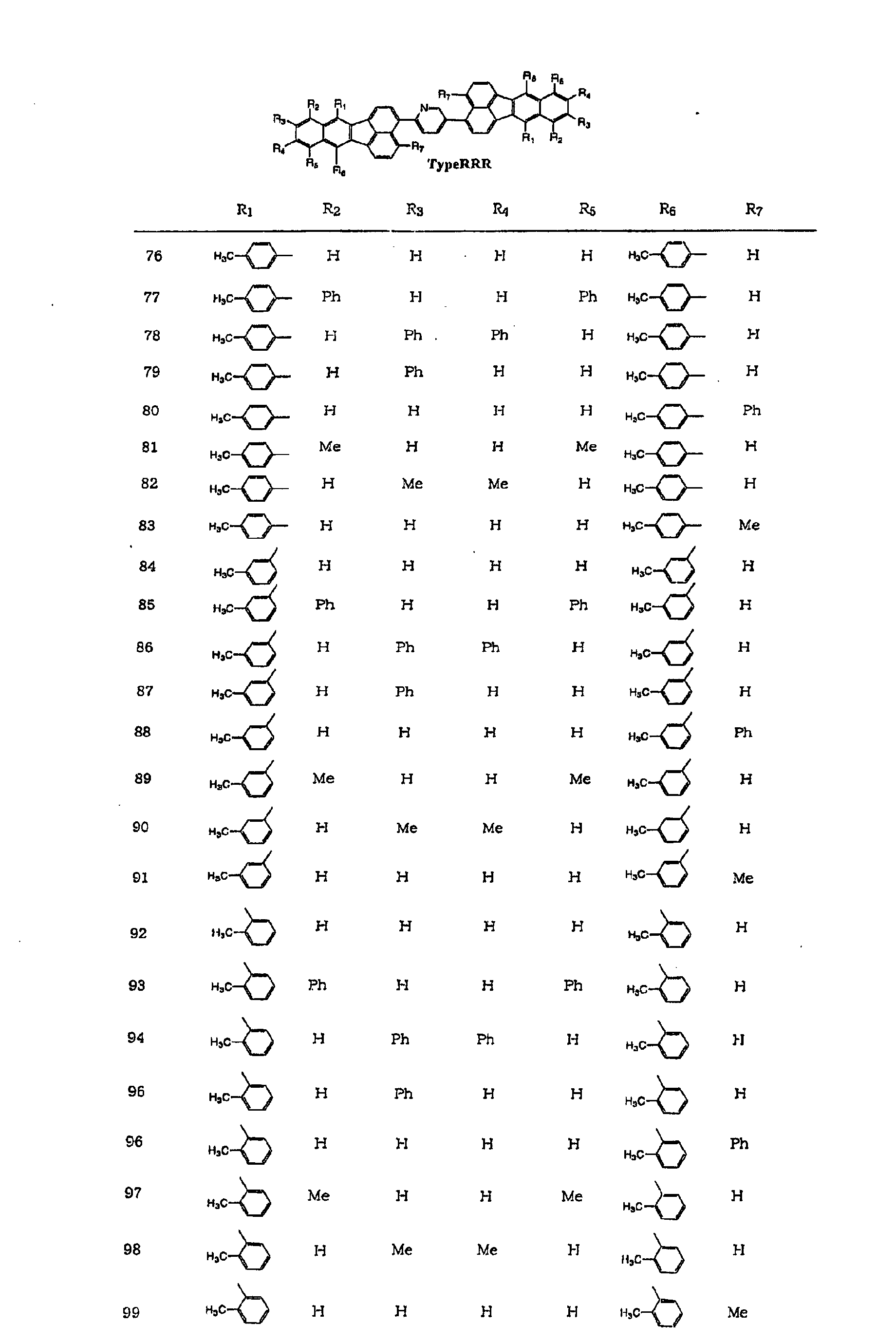
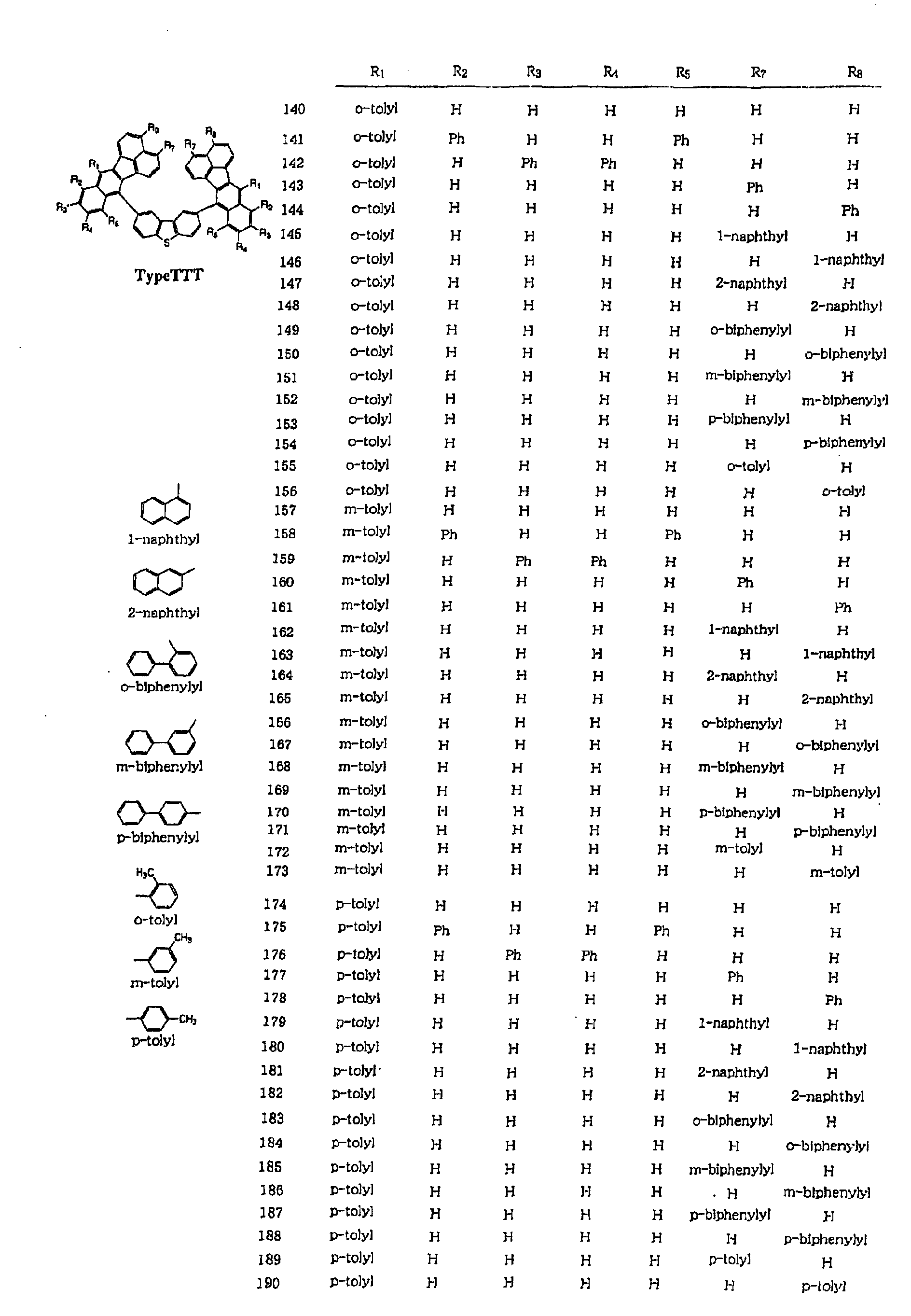
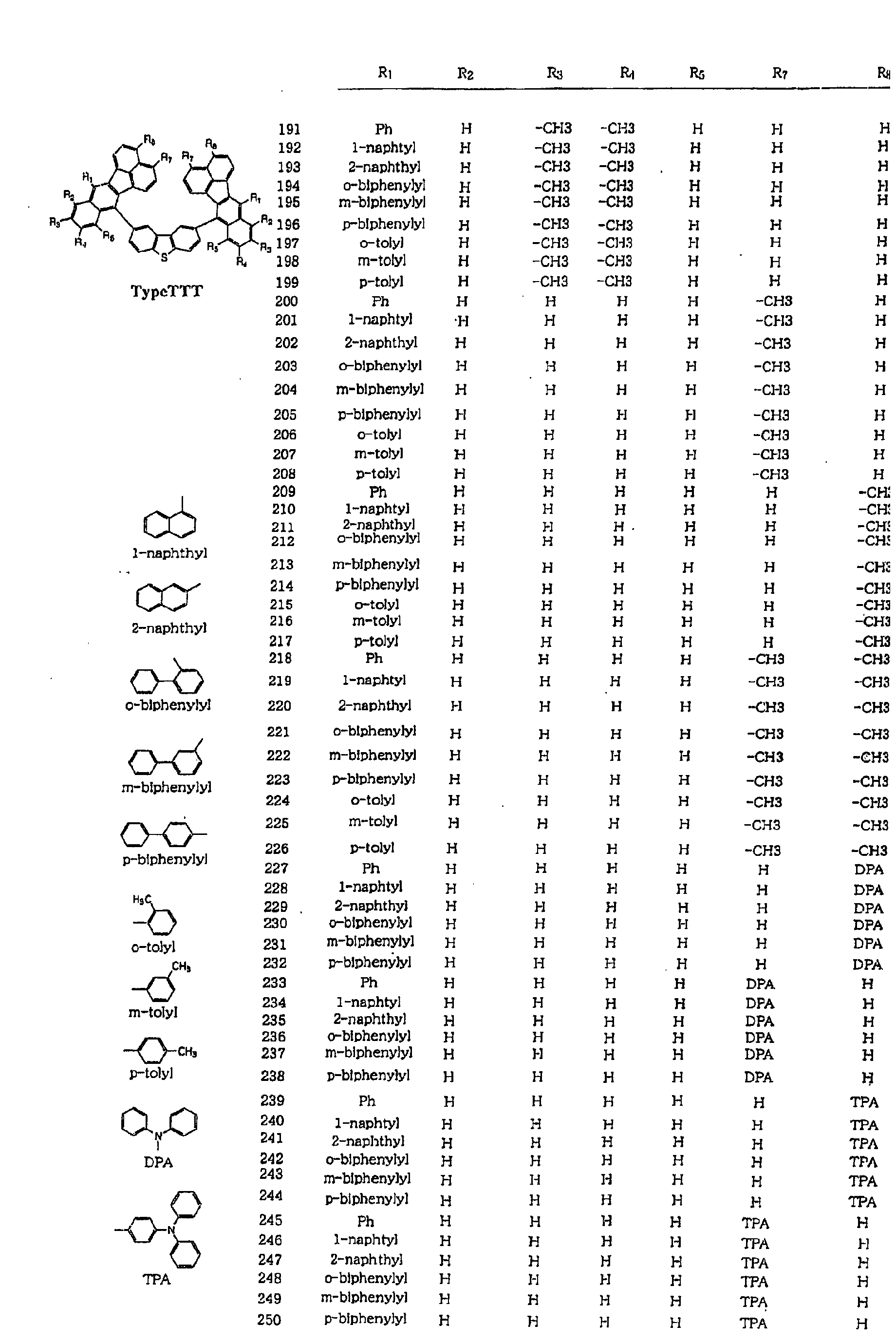
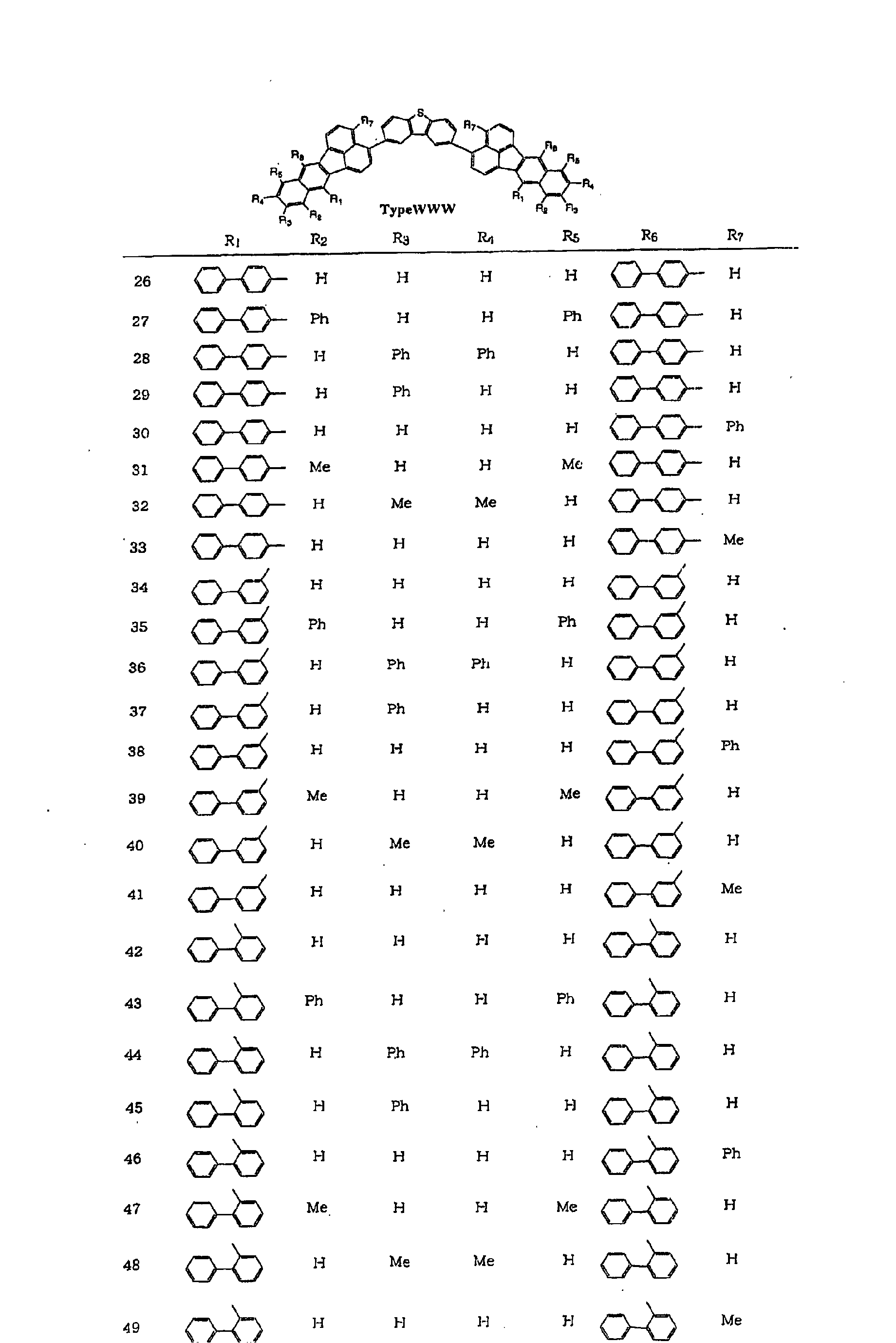
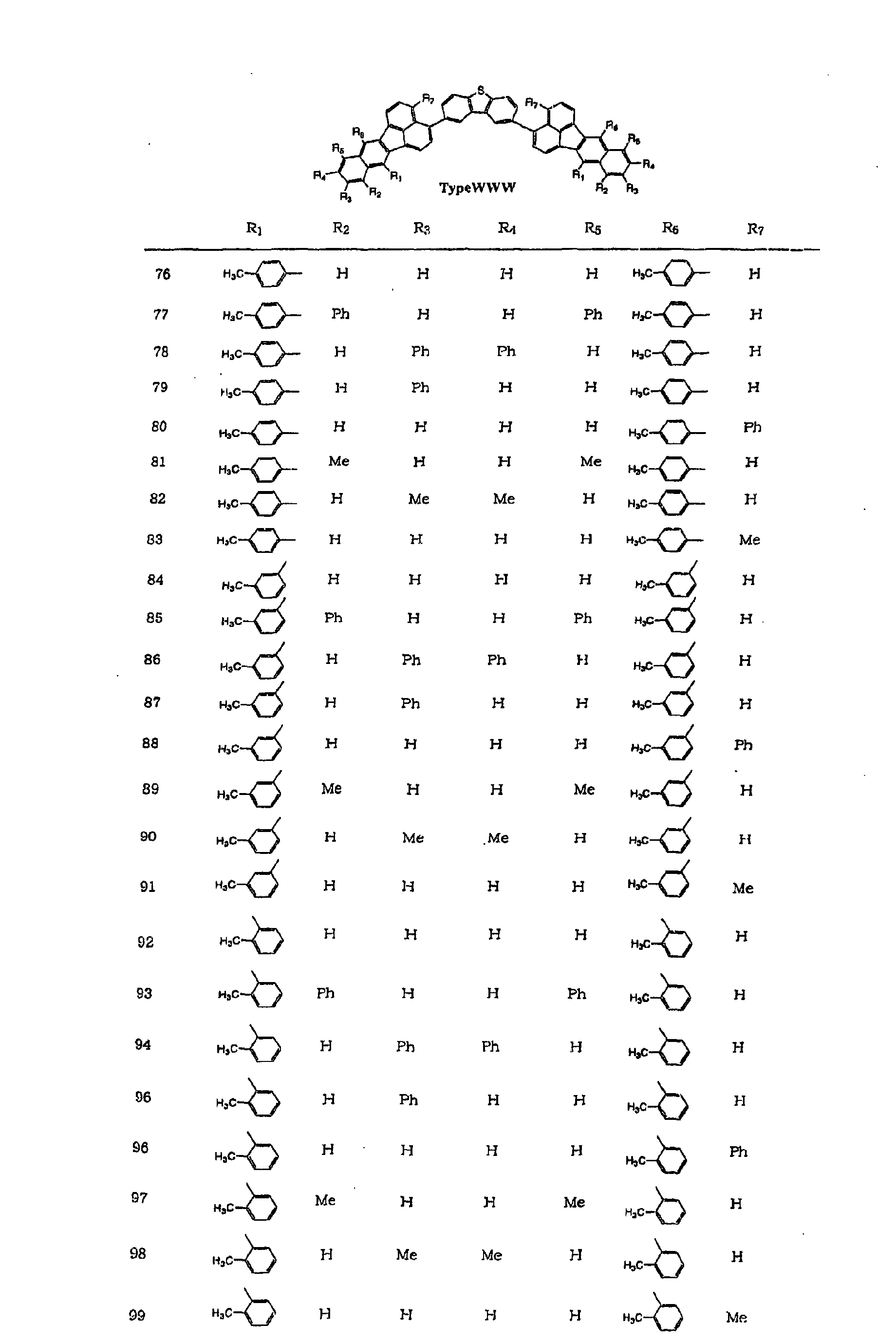
- R 1 to R 8 and a to d each are hydrogen, an alkyl group, an aryl group which may be substituted, an allyl group which may be substituted, a heterocyclic group which may be substituted, an amino group, or an arylamino group which may be substituted.
- R 1 to R 8 and a to d each are hydrogen, an alkyl group, an aryl group which may be substituted, an allyl group which may be substituted, a heterocyclic group which may be substituted, an amino group, or an arylamino group which may be substituted.
- They are preferably selected from among methyl, ethyl, propyl, phenyl, tolyl, biphenyl, naphthyl, thiophenyl, pyridyl, pyrrole, styryl, triphenylamino, and phenylamino groups, and especially from among methyl, phenyl, tolyl, biphenyl, naphthyl, triphenylamino, and phenylamino groups.
- R 1 to R 8 and a to d may be the same or different. Also, adjoining ones of R 1 to R 8 and a to d may form a fused ring.
- R 7 and R 8 preferably have substituents because the structure allows for a high reactivity to these sites. By masking the sites of R 7 and R 8 with substituents, the compounds can be made chemically stable and prevented from degradation during EL light emission. It is preferred that at least either one of R 7 and R 8 have a substituent, and especially both have substituents.
- R 7 and R 8 include those enumerated above, with alkyl, aryl, allyl and heterocyclic groups being especially preferred.
- Y is a linking group selected from among a single bond, a substituted or unsubstituted aryl group, and a heterocyclic group.
- Y bonds X's together in a positional combination of R 7 with R 7 , R 8 with R 8 or R 7 with R 8 a single bond and naphthalene and anthracene compounds having bond positions as shown by the following formulae (11) and (12) are excluded.
- the link positions between X's are not critical. X's may be linked at any position on X or by any carbon on the linking group. Namely, in the basic skeleton represented by the formula (2), the link position may be any position of R 1 to R 8 and a to d, preferably any site selected from among R 1 to R 8 , and especially any site selected from among R 1 , R 6 , R 7 and R 8 .
- Y bonds at the position of R 7 or R 8 a single bond, that is, the event where X's are directly bonded together, and naphthalene and anthracene linking groups at the above-illustrated bond sites are excluded. If X's are directly bonded together at the position of R 7 or R 8 , the compound loses thermal stability during sublimation purification and electrochemical stability during EL light emission, or bonding at the two positions of R 7 and R 8 (symmetric positions) can occur.
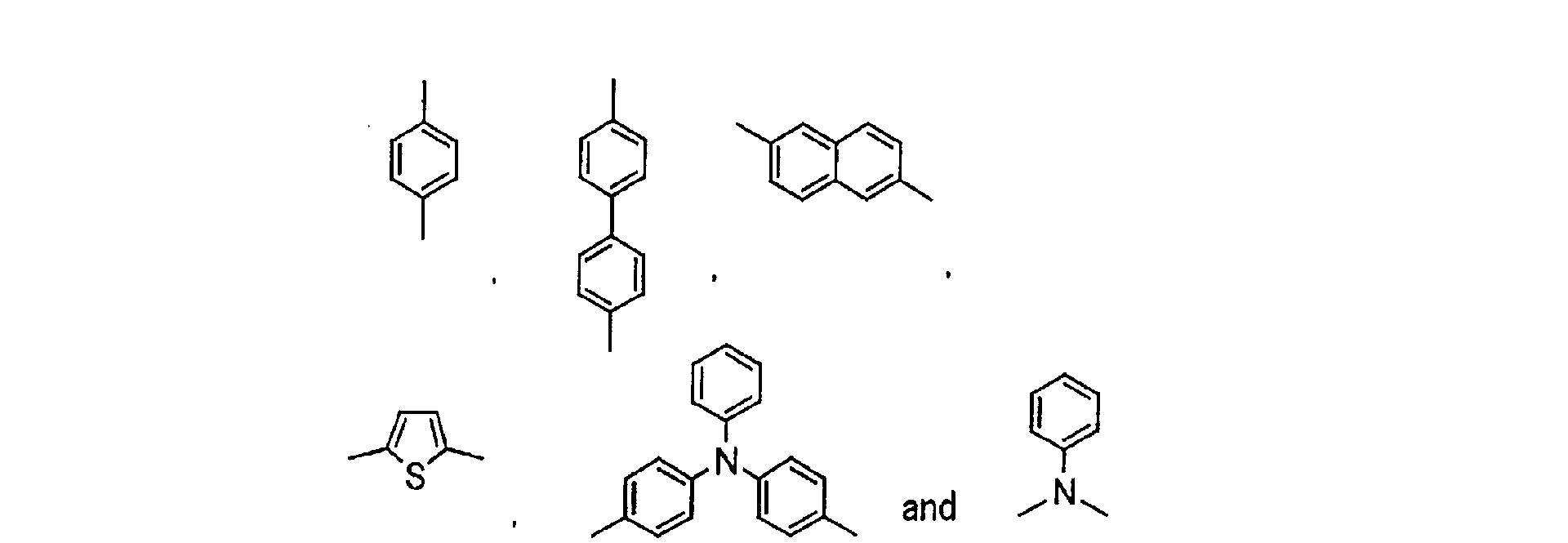
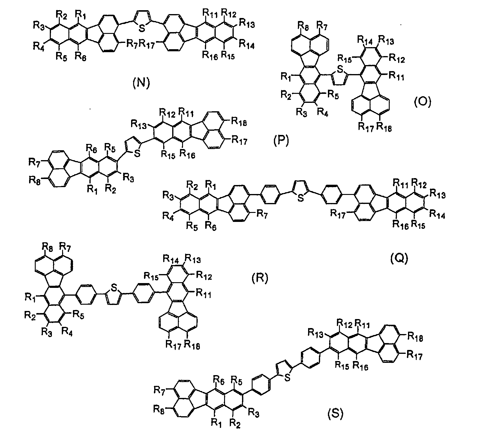
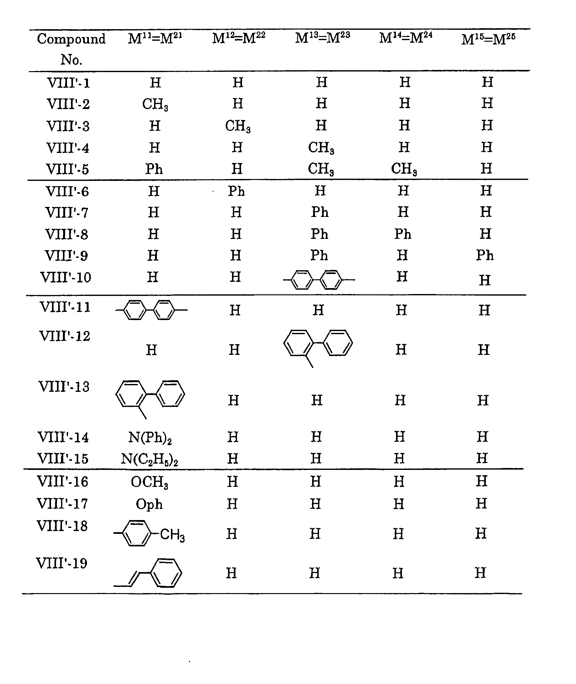
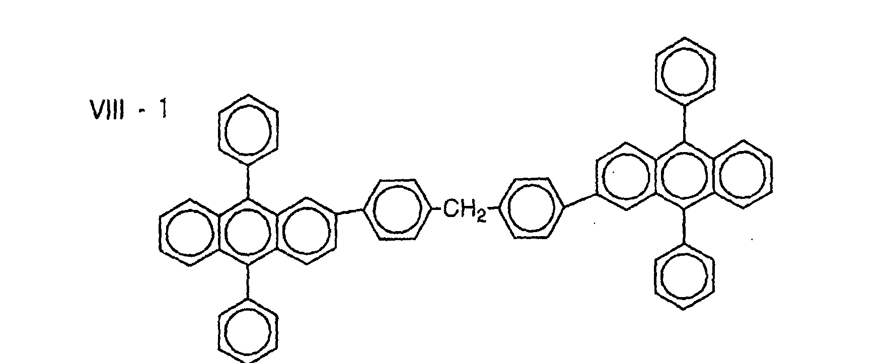
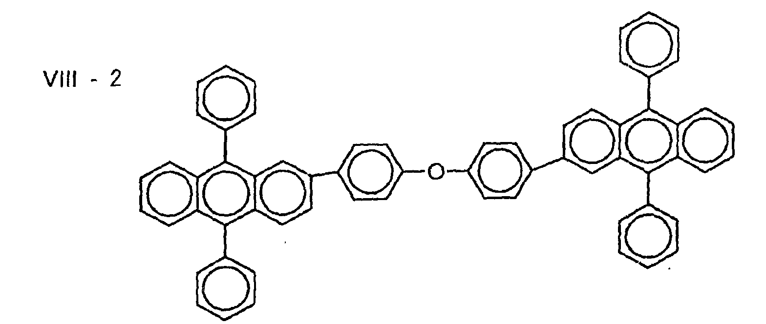
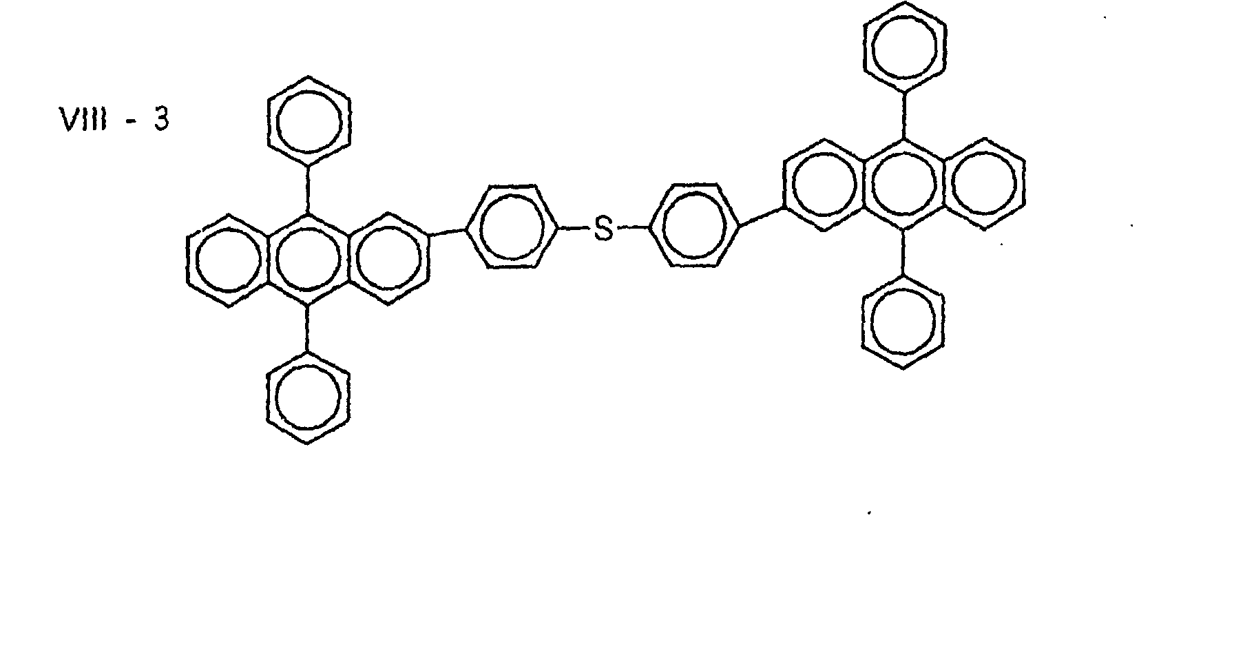
- Y is preferably a linking group selected from among substituted or unsubstituted phenylene, biphenylene, naphthacene, perylene, pyrene, phenanthrene, thiophene, pyridine, pyrazine, triazine, amine, triarylamine, pyrrole derivatives, thiazole, thiadiazole, phenanthroline, quinoline, and quinoxaline, and more preferably from among substituted or unsubstituted benzene, tetracene, perylene, pyrene and heterocyclic groups. More preferably, Y is a linking group of one type selected from the following compounds.
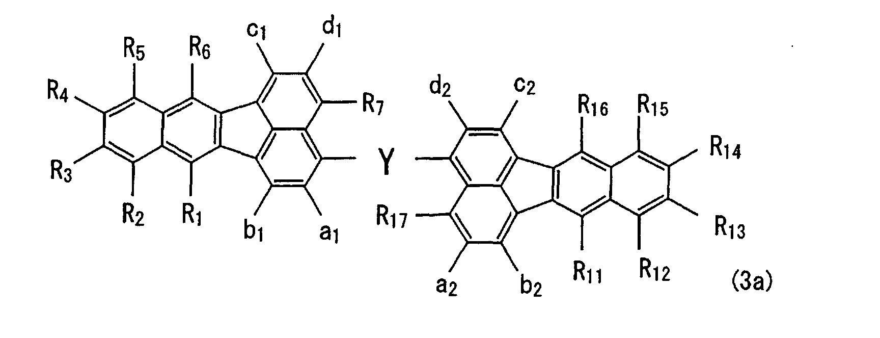
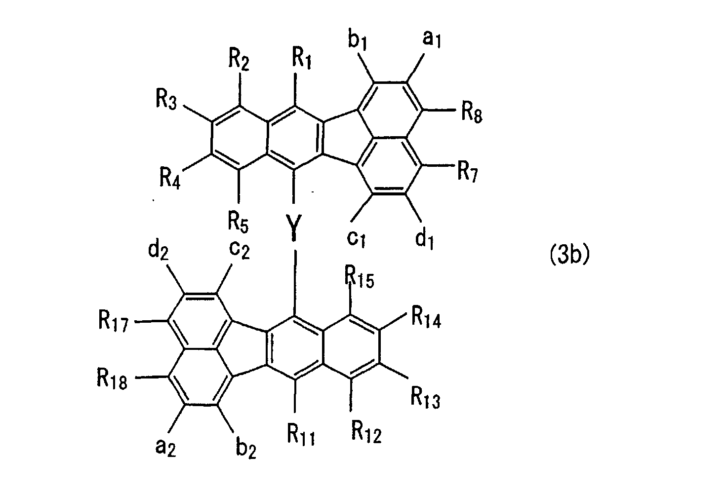
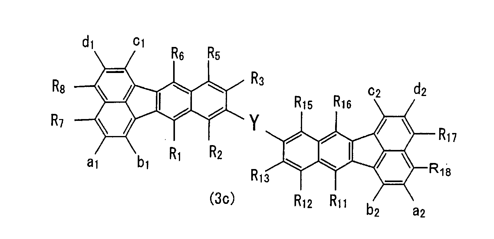
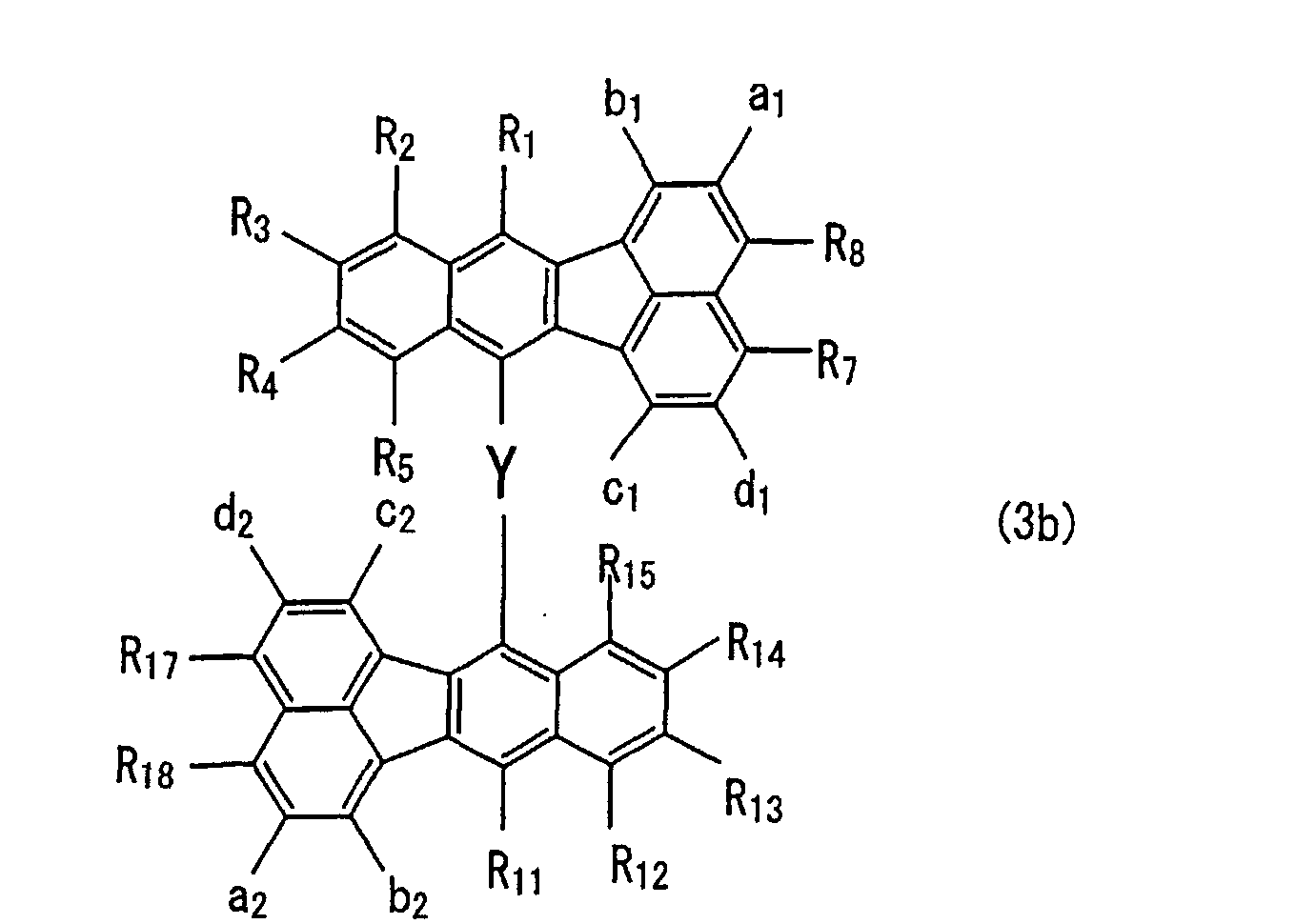
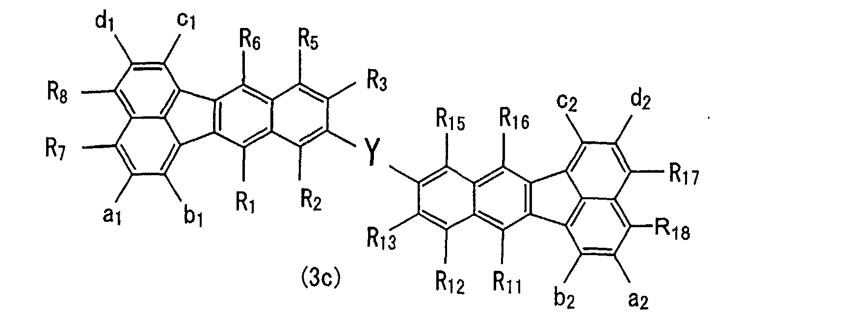
- X is preferably selected from compounds of the following formulae (3a), (3b) and (3c).
- R 1 to R 8 , a 1 to d 1 , R 11 to R 18 and a 2 to d 2 are as defined for R 1 to R 8 and a to d in formula (2).
- the compounds of formula (3a) are most preferred, and the compounds of formula (3b) are preferred next.
- the compounds of the invention should preferably have an absolute value of ionization potential of less than 5.9 eV, more preferably up to 5.8 eV, and even more preferably up to 5.7 eV.
- Compounds with an absolute value of ionization potential of less than 5.9 eV provide satisfactory light emission when combined with those compounds having an absolute value of ionization potential of about 5.9 eV, especially anthracene dimers.
- the lower limit of ionization potential is not critical and is usually about 5.2 eV.
- the compounds of the invention should preferably have a half-wave oxidation potential of up to 1.5 V, more preferably up to 1.4 V, and even more preferably up to 1.3 V, as measured with a platinum electrode in a methylene chloride solution.
- Compounds with an oxidation potential up to the above-specified value are more stable, providing a longer device life. The same effects as the ionization potential are also obtained.
- the lower limit of oxidation potential is not critical and is usually about 0.4 V.
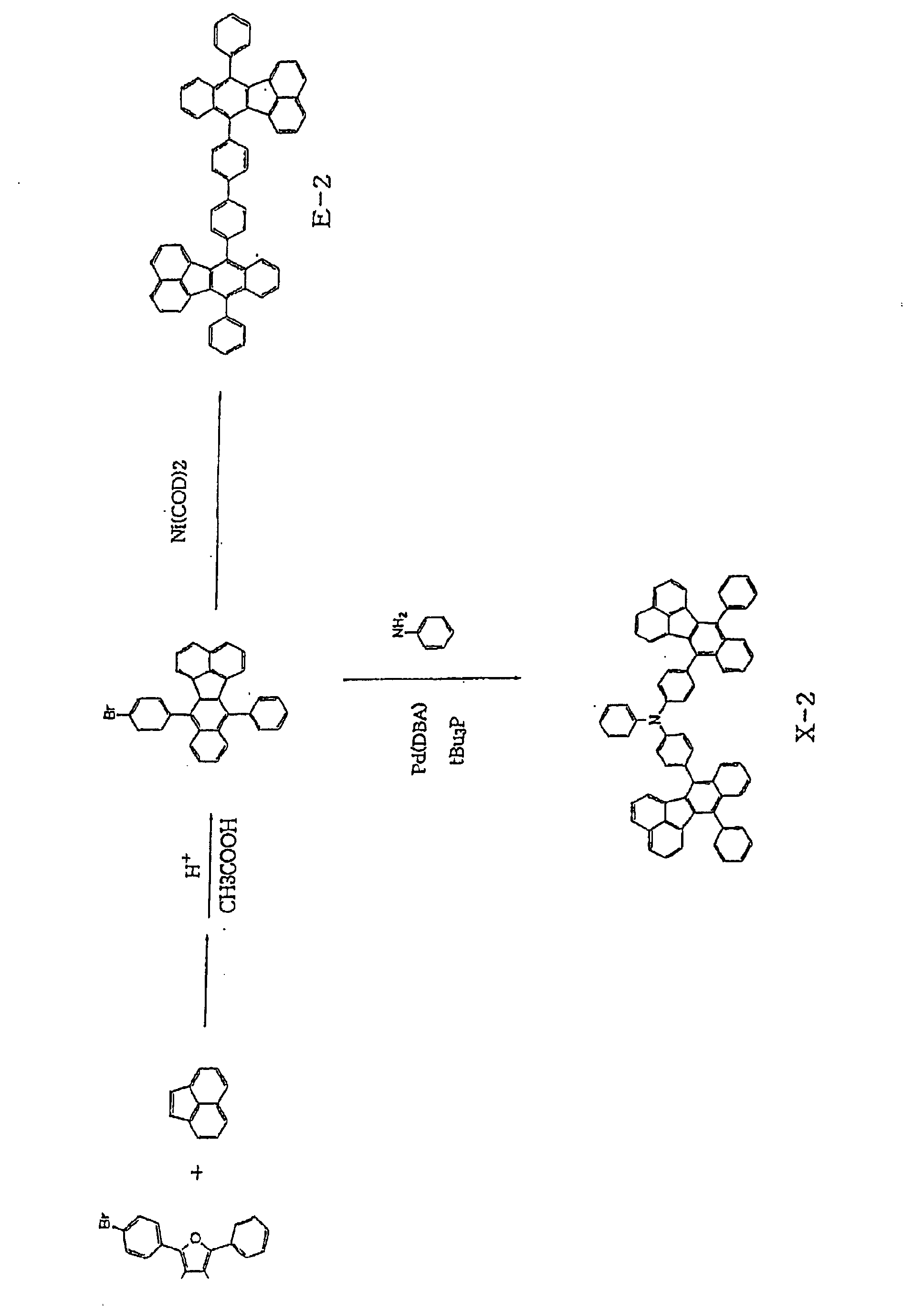
- the fluoranthene derivatives of formula (I) can be produced, for example, by the method described in J. Amer. Chem. Soc., 118, 2374 (1996). Exemplary synthesis schemes are shown below.
- the compounds of the invention are very stable, and exhibit properties which remain constant in the steps involved in the manufacture of organic EL devices such as evaporation and coating, and maintain such consistent properties over a long time even after the manufacture.
- the compounds of the invention When the compounds of the invention are used in organic EL devices, they may serve as either the host material or the dopant. Especially when the compounds are used as the dopant, excellent color and efficiency of light emission as mentioned above are obtainable. Since the compounds of the invention have all of electron injecting and transporting properties, and hole injecting or transporting properties, they can be used as either the electron transporting material or the hole injecting or transporting material.
- the compound of the invention when used in the light emitting layer, it may be serve as either the host material or the dopant, and more preferably as the dopant for blue light emission.
- the host material to be used in combination is preferably an anthracene material. It is also preferred to use a mix layer comprising a mixture of an electron transporting material and a hole transporting material as the host.
- the light emitting layer may contain one or more compounds in addition to the inventive compound. By using such a plurality of compounds in a light emitting layer or stacking light emitting layers of different compounds, the resulting light emitting layer or device can have a plurality of peak wavelengths or a wide range of light emission wavelength.
- fluorescent materials for organic EL devices may be used as the dopant.
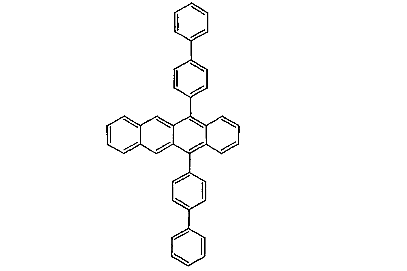
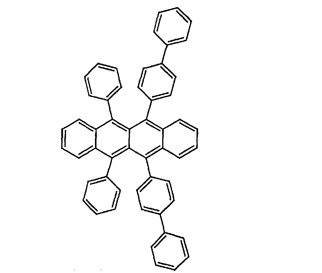
- rubrene derivatives of naphthacene series and diphenylnaphthacene derivatives used in Examples, perylene red fluorescent materials, pentacene red fluorescent materials and distyrylamine derivative materials are preferred.
- the compound of the invention when included in the hole injecting and transporting layer, it may be used as either the hole transporting material or the light emitting material.
- the inventive compound when used as the hole transporting material, the dopant is selected from the aforementioned compounds.
- the compound of the invention when included in the electron injecting and transporting layer, it may be used as either the electron transporting material or the light emitting material.
- the inventive compound when used as the electron transporting material, the dopant is selected from the aforementioned compounds.
- This electron injecting and transporting layer may also be a mix layer as mentioned above.
- the dopant content is preferably up to 30% by weight, more preferably 0.1 to 20% by weight, even more preferably 0.1 to 10% by weight, and especially 0.1 to 5% by weight.
- the light emitting layer containing the host material and the dopant as mentioned above has functions of injecting holes and electrons, transporting them, and recombining holes and electrons to create excitons.
- the use of relatively electronically neutral compounds in the light emitting layer in addition to the compounds of the invention enables easy and well-balanced injection and transportation of electrons and holes.
- the host material may be used alone or in admixture of two or more. When a mixture of two or more host materials is used, the mix ratio is arbitrary. When the compound of the invention is used as the host material, it is preferably contained in an amount of 80 to 99.9%, more preferably 90 to 99.9%, even more preferably 95.0 to 99.5% by weight of the light emitting layer.
- the thickness of the light emitting layer preferably ranges from the thickness corresponding to a single molecule layer to less than the thickness of an organic compound layer, for example, preferably from 1 to 85 nm, more preferably 5 to 60 nm, and most preferably 5 to 50 nm.
- the mix layer is formed by a co-deposition process of evaporating the compounds from distinct sources. If both the compounds have equal or very close vapor pressure or evaporation temperature, they may be pre-mixed in a common evaporation boat, from which they are evaporated together.
- the mix layer is preferably a uniform mixture of both the compounds although the compounds can be present in island form.
- the light emitting layer is generally formed to a predetermined thickness by evaporating an organic fluorescent material or coating a dispersion thereof in a resin binder.
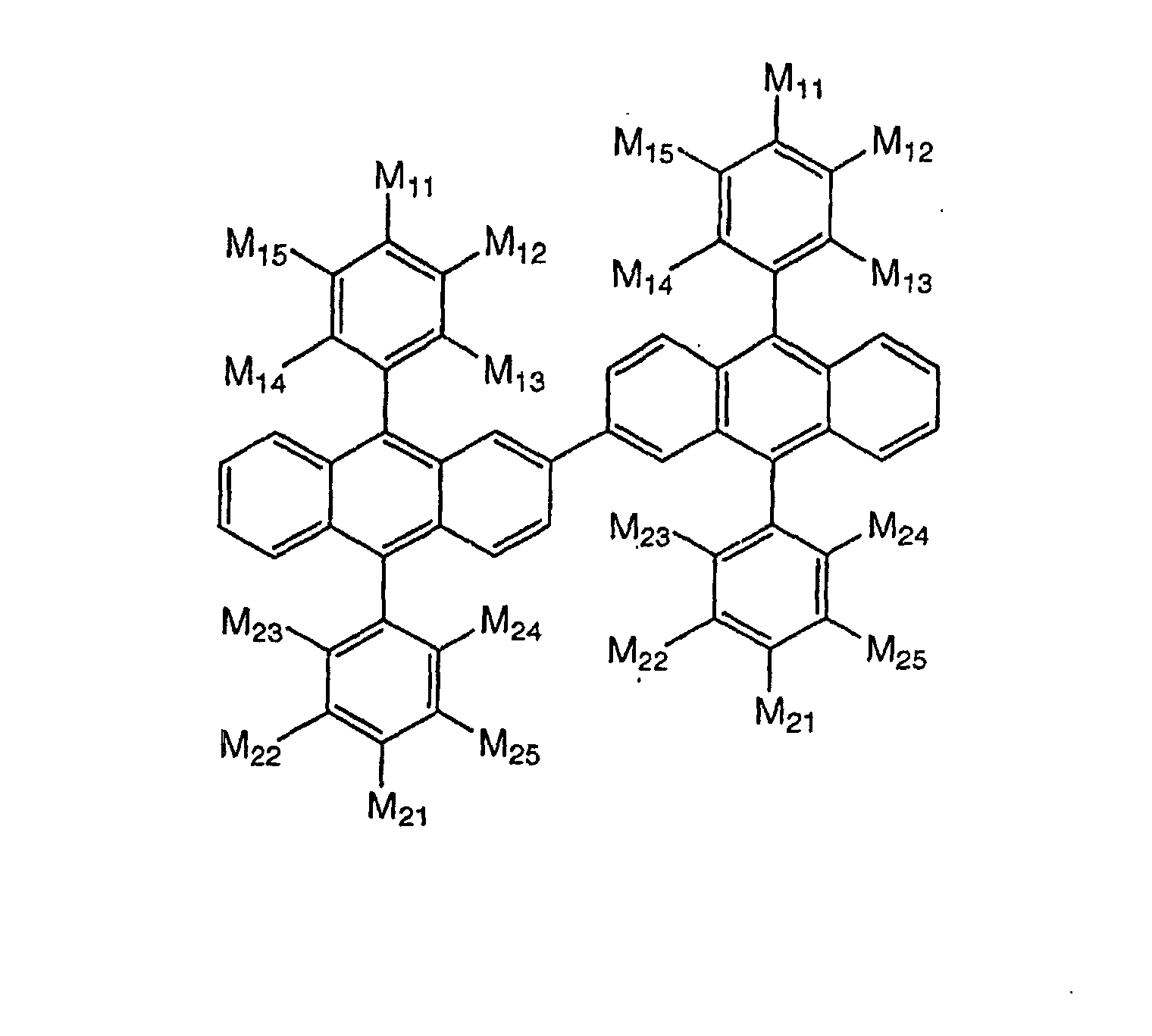
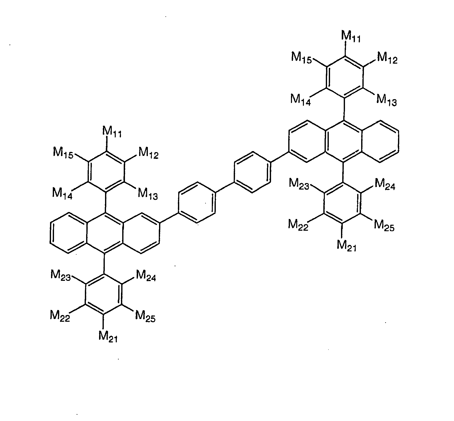
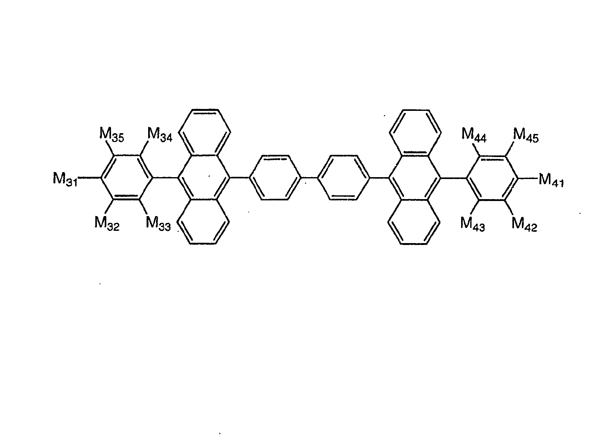
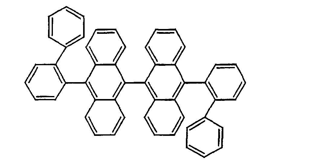
- a class of organic compounds preferred as the host material in devices according to the invention are phenylanthracene derivatives of the following formula (5).
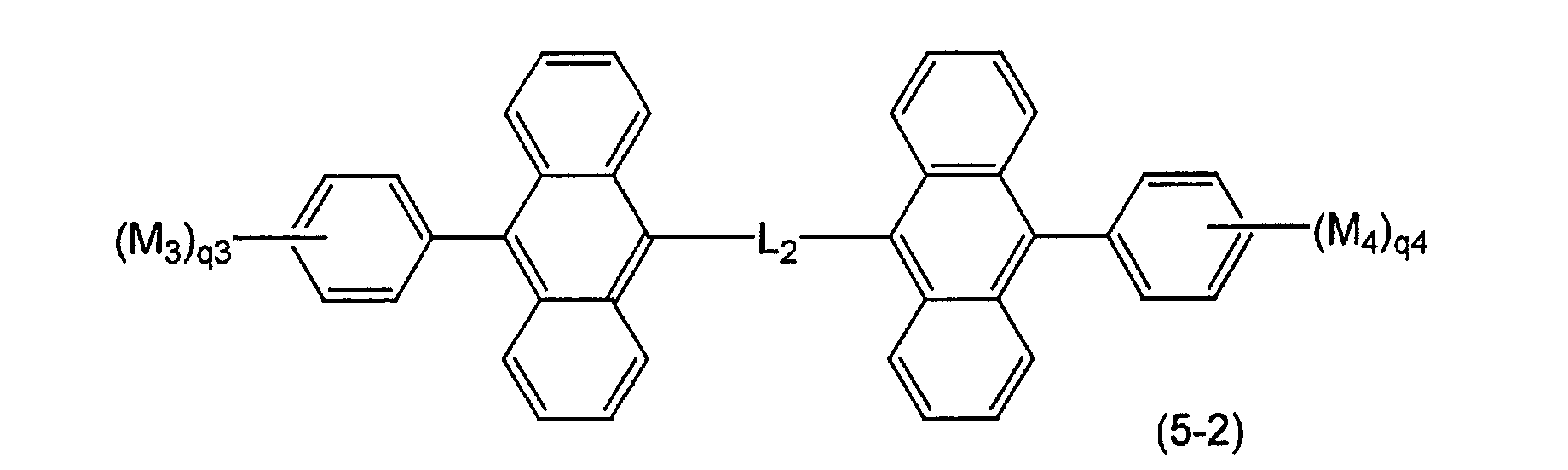
- the use of the anthracene derivative of formula (5), typically formula (5-1) or (5-2), preferably as the host material, helps induce strong light emission from the dopant while controlling the interaction with the dopant. Since the anthracene derivatives are fully heat resistant and durable, devices with a longer lifetime are obtainable.
- the dopant concentration ensuring a color purity and maximum efficiency is about 1% by weight although dopant concentrations of about 2 or 3% by weight lead to devices which are practically acceptable albeit a drop of less than about 10%.
- a 101 is a monophenylanthryl or diphenylanthryl radical and may be the same or different, L is hydrogen, a single bond or a divalent linkage, and n is an integer of 1 or 2.
- Evaporated films of these compounds remain in a stable amorphous state, that is, have sufficient physical properties to produce consistent uniform light emission.
- the films remain stable over one year in the ambient atmosphere without crystallization.
- a 101 is a monophenylanthryl or diphenylanthryl radical and may be the same or different, and n is an integer of 1 or 2.
- the monophenylanthryl or diphenylanthryl radical represented by A 101 may be substituted or unsubstituted.
- suitable substituents if any, are alkyl, aryl, alkoxy, aryloxy and amino groups. These substituents may further have substituents thereon and will be described later.
- the position of a substituent on the monophenylanthryl or diphenylanthryl radical is not critical although the preferred substitution position is on the phenyl group bonded to the anthracene ring rather than the anthracene ring.
- the phenyl group is bonded to the anthracene ring at the 9- and 10-positions.
- L is hydrogen, a single bond or a divalent linkage.
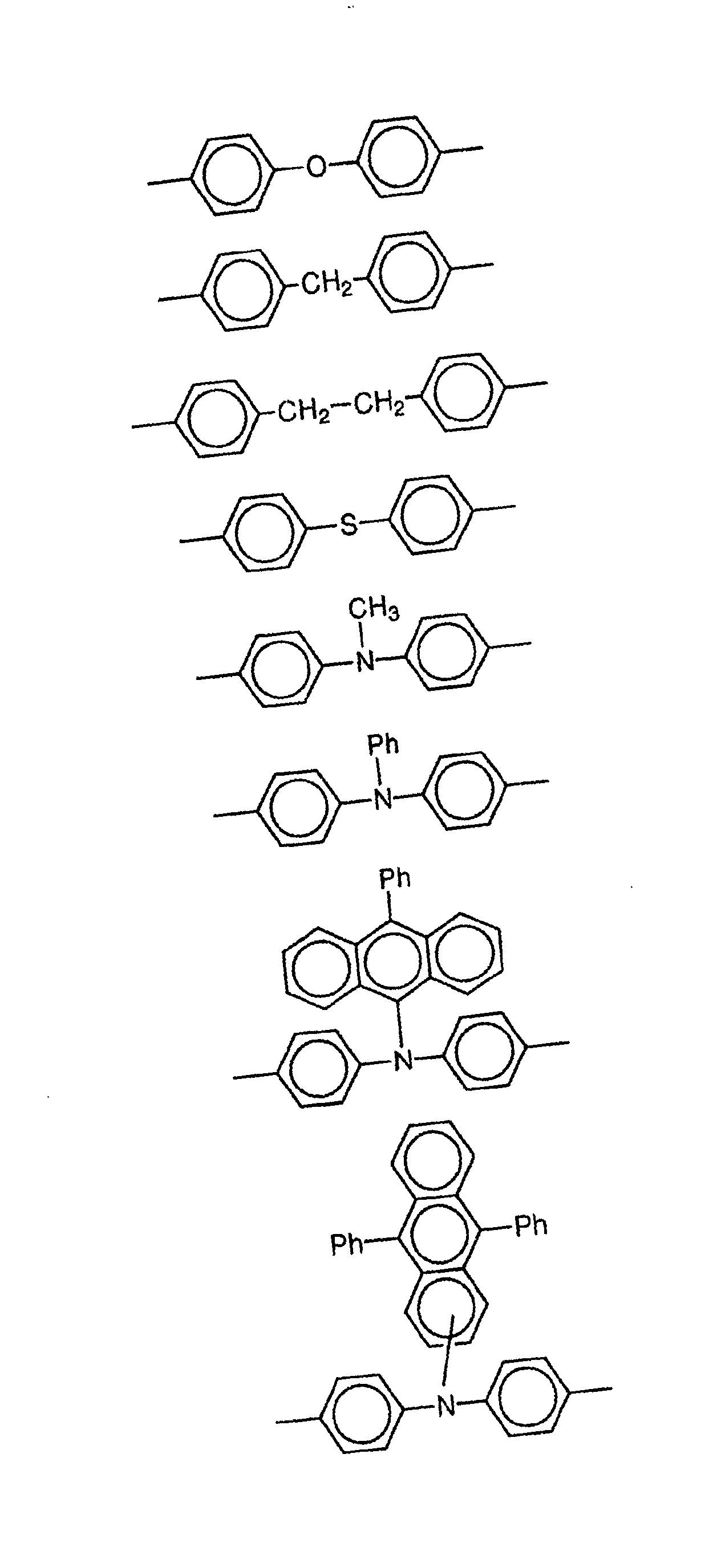
- the divalent linkage represented by L is preferably an arylene radical which may be separated by an alkylene or analogous group. The arylene radical will be described later.
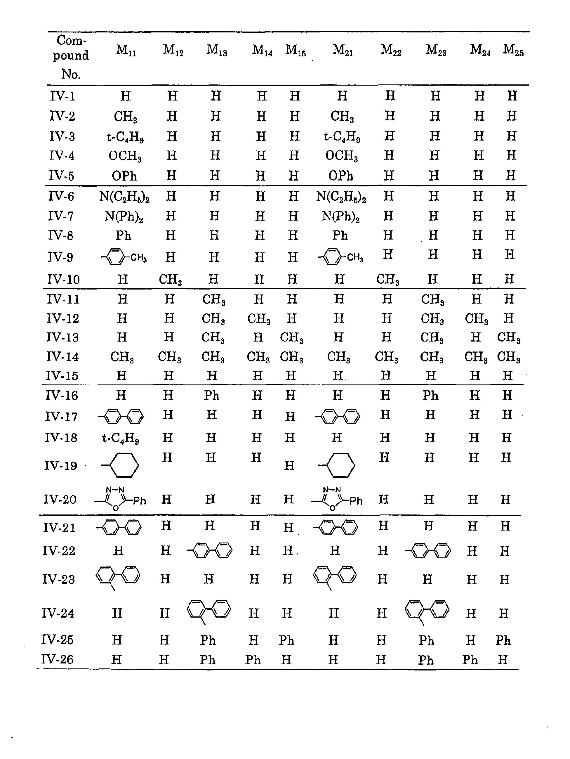
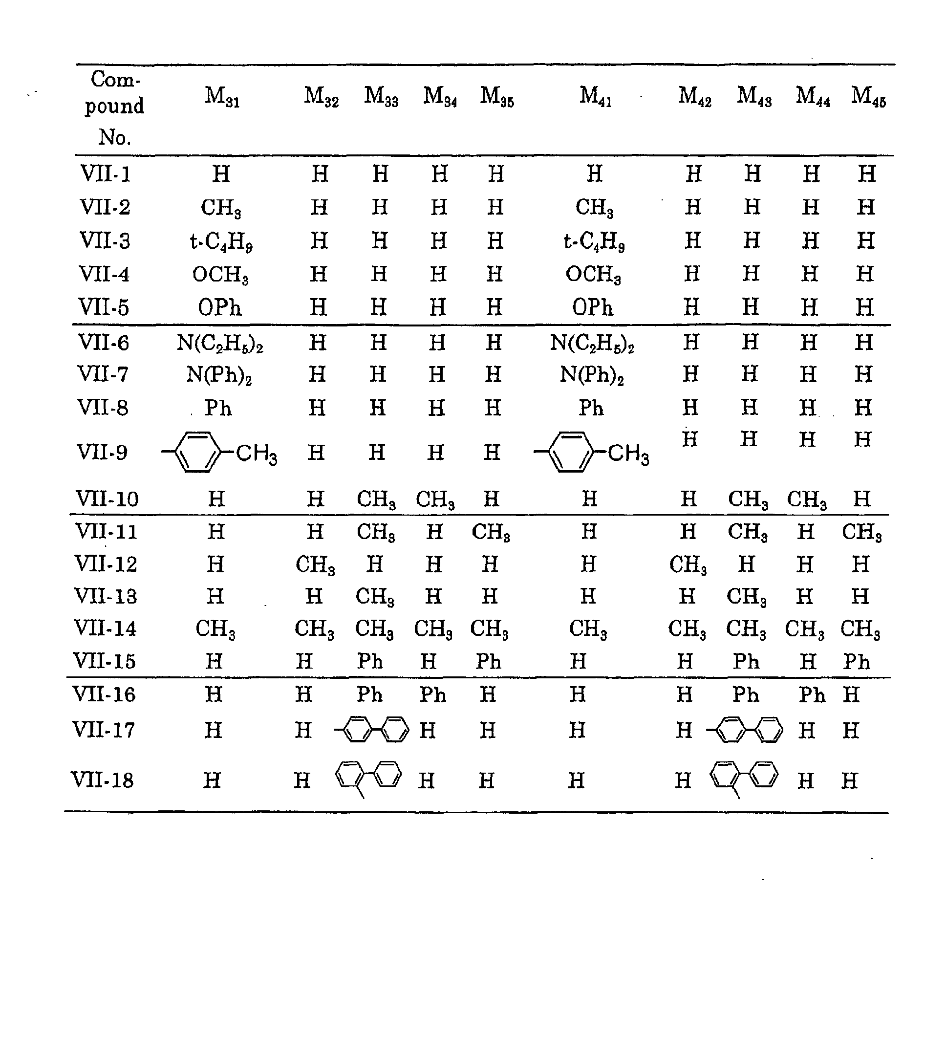
- M 1 and M 2 each are alkyl, cycloalkyl, aryl, alkoxy, aryloxy, amino or heterocyclic radicals.
- the alkyl radicals represented by M 1 and M 2 may be substituted or unsubstituted, straight or branched alkyl radicals, preferably of 1 to 10 carbon atoms, more preferably 1 to 4 carbon atoms. Unsubstituted alkyl radicals of 1 to 4 carbon atoms are preferred, such as, for example, methyl, ethyl, n- and i-propyl, and n-, i-, sec-and tert-butyl.
- Exemplary of the cycloalkyl radicals represented by M 1 and M 2 are cyclohexyl and cyclopentyl.
- the aryl radicals represented by M 1 and M 2 are preferably those aryl radicals having 6 to 20 carbon atoms which may have substituents such as phenyl and tolyl.
- Preferred examples of the aryl radical include phenyl, o-, m- and p-tolyl, pyrenyl, naphthyl, anthryl, biphenyl, phenylanthryl and tolylanthryl.
- alkenyl radicals represented by M 1 and M 2 are preferably those having 6 to 50 carbon atoms in total, which may be substituted or unsubstituted, with the substituted ones being preferred. Such substituents are aryl groups such as phenyl. Exemplary alkenyl radicals are triphenylvinyl, tritolylvinyl and tribiphenylvinyl.
- the alkoxy radicals represented by M 1 and M 2 are preferably those having an alkyl moiety of 1 to 6 carbon atoms, for example, methoxy and ethoxy.
- the alkoxy radicals may have substituents.
- Exemplary of the aryloxy radicals represented by M 1 and M 2 is phenoxy.
- the amino radicals represented by M 1 and M 2 may be substituted or unsubstituted, with the substituted amino radicals being preferred.
- substituents are alkyl groups such as methyl and ethyl and aryl groups such as phenyl.
- Illustrative examples of the amino radical include diethylamino, diphenylamino and di(m-tolyl)amino radicals.
- the heterocyclic radicals represented by M 1 and M 2 include bipyridyl, pyrimidyl, quinolyl, pyridyl, thienyl, furyl and oxadiazoyl radicals and may have substituents such as methyl and phenyl.
- q1 and q2 each are 0 or an integer of 1 to 5, especially 0 or 1.
- M 1 and M 2 each are preferably alkyl, aryl, alkenyl, alkoxy, aryloxy or amino radicals.
- M 1 and M 2 may be the same or different. Where a plurality of M 1 or M 2 are included, the M 1 groups or M 2 groups may be the same or different. Alternatively, the M 1 groups or M 2 groups bond together to form a ring such as a benzene ring. The ring formation is also a preferred embodiment.
- L 1 is hydrogen, a single bond or an arylene radical.
- the arylene radicals represented by L 1 are preferably unsubstituted ones, for example, ordinary arylene radicals such as phenylene, biphenylene and anthrylene as well as two or more arylene radicals which are directly bonded.
- L 1 is preferably a single bond, p-phenylene or 4,4'-biphenylene.
- the arylene radical represented by L 1 may consist of two or more arylene radicals which are connected by an alkylene radical, -O-, -S- or -NR- wherein R is an alkyl or aryl radical.
- alkyl radicals are methyl and ethyl, and an exemplary aryl radical is phenyl.
- R is preferably an aryl radical, such as phenyl.
- R is A 101 or a phenyl radical having A 101 substituted thereon.
- alkylene radicals are preferably methylene and ethylene.
- Illustrative examples of the arylene radical are given below.
- M 3 and M 4 are the same as M 1 and M 2 in formula (5-1), q3 and q4 are the same as q1 and q2 in formula (5-1), and L 2 is the same as L 1 in formula (5-1). Preferred examples of these radicals are also the same.
- M 3 and M 4 may be the same or different. Where a plurality of M 3 or M 4 are included, the M 3 groups or M 4 groups may be the same or different. Alternatively, the M 3 groups or M 4 groups bond together to form a ring such as a benzene ring. The ring formation is also a preferred embodiment.
- phenylanthracene derivatives used herein can be prepared by
- the phenylanthracene derivatives have a molecular weight of about 400 to about 2,000, preferably about 400 to about 1,000, a high melting point of about 200 to about 500°C, and a high glass transition temperature (Tg) of about 80 to about 250°C, preferably about 100 to 250°C, more preferably about 130 to 250°C, especially about 150 to 250°C.
- Tg glass transition temperature
- phenylanthracene derivatives are relatively neutral compounds, better results are obtained on use of them in a light emitting layer.
- a freedom of design of the recombination/light emitting region is available by controlling the film thickness in consideration of the carrier mobility and carrier density (which is dependent on ionization potential and electron affinity) of the light emitting layer, hole injecting and transporting layer, and electron injecting and transporting layer to be combined. This enables free design of luminous color, control of the luminance and spectrum of light emission by the interference of the electrodes, and control of the space distribution of light emission.
- One exemplary construction of the organic EL light emitting device fabricated using the inventive compounds has on a substrate, a hole injecting electrode, a hole injecting and transporting layer, a light emitting and electron injecting and transporting layer, and an electron injecting electrode in the described order. If desired, an auxiliary electrode and a sealing layer are provided on the electron injecting electrode.
- the organic EL device of the invention is not limited to the above exemplary construction and may have various other constructions.
- the light emitting layer is provided singly and an electron injecting and transporting layer is interposed between the light emitting layer and the electron injecting electrode.
- the light emitting layer may be mixed with the hole injecting and transporting layer, if desired.
- the thicknesses of the light emitting layer, hole injecting and transporting layer, and electron injecting and transporting layer are not critical and vary with a particular formation technique. Usually a single layer is about 5 to 500 nm thick, especially about 10 to 300 nm thick.
- the thicknesses of the hole injecting and transporting layer and electron injecting and transporting layer are equal to or range from 1/10 to 10 times the thickness of the light emitting layer although they depend on the design of a recombination/light emitting region.
- the electron or hole injecting and transporting layer is divided into an injecting layer and a transporting layer, preferably the injecting layer is at least 1 nm thick and the transporting layer is at least 1 nm thick.
- the upper limit of thickness is generally about 500 nm for the injecting layer and about 500 nm for the transporting layer. The same applies when two injecting and transporting layers are provided.
- the hole injecting and transporting layer has functions of facilitating injection of holes from the hole injecting electrode, transporting them stably, and blocking electrons.
- the electron injecting and transporting layer has functions of facilitating injection of electrons from the electron injecting electrode, transporting them stably, and blocking holes. These layers are effective for increasing the number of holes and electrons injected into the light emitting layer and confining holes and electrons therein for optimizing the recombination region to improve light emission efficiency.
- the hole injecting and transporting layer aside from the inventive compounds, there may be used various organic compounds as described, for example, in JP-A 63-295695, 2-191694, 3-792, 5-234681, 5-239455, 5-299174, 7-126225, 7-126226, and 8-100172, and EPO 650955A1.
- exemplary are tetraarylbenzidine compounds (triaryldiamines or triphenyldiamines: TPD), aromatic tertiary amines, hydrazone derivatives, carbazole derivatives, triazole derivatives, imidazole derivatives, oxadiazole derivatives having an amino group, and polythiophenes. Two or more of these compounds may be used, and on such combined use, they may be formed as separate layers or mixed.
- the hole injecting and transporting layer is formed separately as a hole injecting layer and a hole transporting layer
- two or more compounds are selected in a proper combination from the compounds commonly used in hole injecting and transporting layers.
- laminate layers in such an order that a layer of a compound having a lower ionization potential may be disposed adjacent the hole injecting electrode (ITO).
- ITO hole injecting electrode
- the order of lamination also applies where a plurality of hole injecting and transporting layers are provided. Such an order of lamination is effective for lowering the drive voltage and preventing current leakage and the development and growth of dark spots.
- the hole injecting and transporting layer may be formed by evaporating the above-mentioned compounds.
- the electron injecting and transporting layer aside from the inventive compounds, there may be used quinoline derivatives including organic metal complexes having 8-quinolinol or a derivative thereof as a ligand such as tris(8-quinolinolato)aluminum (Alq3), oxadiazole derivatives, perylene derivatives, nitrogen-containing heterocyclic aromatics such as pyridine derivatives, pyrimidine derivatives, quinoxaline derivatives and phenanthroline derivatives, diphenylquinone derivatives, and nitro-substituted fluorene derivatives.
- the electron injecting and transporting layer can also serve as the light emitting layer, and in such a case, the light emitting layer according to the invention is preferably employed.
- the electron injecting and transporting layer may be formed by evaporation or the like.
- the electron injecting and transporting layer is formed separately as an electron injecting layer and an electron transporting layer
- two or more compounds are selected in a proper combination from the compounds commonly used in electron injecting and transporting layers.
- the order of stacking also applies where a plurality of electron injecting and transporting layers are provided.
- vacuum evaporation is preferably used because homogeneous thin films are available.
- vacuum evaporation there is obtained a homogeneous thin film which is amorphous or has a crystal grain size of up to 0.1 ⁇ m. If the grain size is more than 0.1 pm, uneven light emission would take place and the drive voltage of the device must be increased with a substantial drop of hole injection efficiency.
- the conditions for vacuum evaporation are not critical although a vacuum of 10 -4 Pa or lower and a deposition rate of about 0.01 to 1 nm/sec are preferred. It is preferred to successively form layers in vacuum because the successive formation in vacuum can avoid adsorption of impurities on the interface between the layers, thus ensuring better performance. Also, the drive voltage of a device can be reduced and the development and growth of dark spots be restrained.
- boats having the compounds received therein are individually temperature controlled to achieve co-deposition.
- the electron injecting electrode is preferably made of metals, alloys or intermetallic compounds having a work function of up to 4 eV. With a work function of more than 4 eV, the electron injecting efficiency lowers and consequently, the light emission efficiency lowers.
- the metal having a work function of up to 4 eV of which the electron injecting electrode film is constructed include alkali metals such as Li, Na and K, alkaline earth metals such as Mg, Ca, Sr and Ba, rare earth metals such as La and Ce, and Al, In, Ag, Sn, Zn, and Zr.
- Examples of the film-forming alloy having a work function of up to 4 eV include Ag-Mg (Ag: 0.1 to 50 at%), Al-Li (Li: 0.01 to 12 at%), In-Mg (Mg: 50 to 80 at%), and Al-Ca (Ca: 0.01 to 20 at%). These materials may be present alone or in combination of two or more. Where two or more materials are combined, their mixing ratio is arbitrary. It is also acceptable that an oxide or halide of an alkali metal, alkaline earth metal or rare earth metal is thinly deposited and a supporting electrode (auxiliary electrode or wiring electrode) of aluminum etc. is used.
- the electron injecting electrode may be formed by evaporation or sputtering.
- the electron injecting electrode may have at least a sufficient thickness to effect electron injection, for example, a thickness of at least 0.1 nm. Although the upper limit is not critical, the electrode thickness is typically about 0.1 to about 500 nm.
- the hole injecting electrode is preferably formed of such a material to such a thickness that the electrode may have a transmittance of at least 80% of emitted light.
- oxide transparent conductive thin films are preferred.
- materials based on tin-doped indium oxide (ITO), zinc-doped indium oxide (IZO), indium oxide (In 2 O 3 ), tin oxide (SnO 2 ) or zinc oxide (ZnO) are preferable. These oxides may deviate somewhat from their stoichiometry.
- An appropriate proportion of SnO 2 mixed with In 2 O 3 is 1 to 20%, more preferably 5 to 12% by weight.
- An appropriate proportion of ZnO 2 mixed with In 2 O 3 is 12 to 32% by weight.
- the hole injecting electrode should preferably have a light transmittance of at least 80%, especially at least 90% in the light emission band, typically from 350 to 800 nm, and especially at each light emission. Since the emitted light is generally taken out through the hole injecting electrode, with a lower transmittance, the light emitted by the light emitting layer would be attenuated through the electrode, failing to provide a luminance necessary as a light emitting device. It is noted that only the side from which the emitted light exits has a transmittance of at least 80%.
- the hole injecting electrode has at least a sufficient thickness to effect hole injection, preferably a thickness of 50 to 500 nm, especially 50 to 300 nm.
- a sufficient thickness to effect hole injection preferably a thickness of 50 to 500 nm, especially 50 to 300 nm.
- the upper limit of the electrode thickness is not critical, a too thick electrode would have the risk of separation. Too thin an electrode would have problems with respect to film strength during fabrication, hole transporting ability, and resistance value.
- a sputtering process is preferred.
- the sputtering process may be a high-frequency sputtering process using an RF power supply although a DC sputtering process is preferably used when the ease of control of physical properties of the hole injecting electrode being deposited and the flatness of the deposited film are taken into account.
- a protective film may be formed if necessary.
- the protective film may be formed using an inorganic material such as SiO x or an organic material such as TeflonTM.
- the protective film may be either transparent or opaque and have a thickness of about 50 to 1,200 nm.
- the protective film may also be formed by an ordinary sputtering or evaporation process.
- a sealing layer is preferably provided on the device in order to prevent the organic layers and electrodes from oxidation.
- the sealing layer is formed by attaching a sealing plate such as a glass plate to the substrate with an adhesive resin layer such as a commercially available low moisture absorption photo-curable adhesive, epoxy base adhesive, silicone base adhesive, or crosslinking ethylenevinyl acetate copolymer adhesive sheet.
- an adhesive resin layer such as a commercially available low moisture absorption photo-curable adhesive, epoxy base adhesive, silicone base adhesive, or crosslinking ethylenevinyl acetate copolymer adhesive sheet.
- Metal plates and plastic plates may also be used instead of the glass plate.
- Transparent or translucent materials such as glass, quartz and resins are used as the substrate when the emitted light exits from the substrate side.
- the substrate may be provided with a color filter film, a fluorescent material-containing color conversion film or a dielectric reflecting film for controlling the color of light emission.
- the substrate may be either transparent or opaque.
- ceramic and other materials may be used for the opaque substrate.
- the color filter film used herein may be a color filter as used in liquid crystal displays and the like.
- the properties of a color filter may be adjusted in accordance with the light emission of the organic EL device so as to optimize the extraction efficiency and chromatic purity.
- a color filter capable of cutting external light of short wavelength which is otherwise absorbed by the EL device materials and fluorescence conversion layer, because the light resistance and display contrast of the device are improved.
- An optical thin film such as a dielectric multilayer film may be used instead of the color filter.
- the organic EL device of the invention is constructed, as shown in FIG. 1, for example, to have on a substrate 1, a hole injecting electrode (or anode) 2, a hole injecting and transporting layer 3, a light emitting layer 4, an electron injecting and transporting layer 5, and an electron injecting electrode (or cathode) 6 in the described order.
- the order of lamination may be inverse to the above-described order.
- the hole injecting and transporting layer 3 and the electron injecting and transporting layer 5 may be omitted or either one of them may be a common layer to the light emitting layer 4.
- Each of these constituent layers may be adjusted optimum depending on the required function of the device.
- the organic EL device of the invention is generally of the DC or pulse drive type while it can be of the AC drive type.
- the applied voltage is generally about 2 to 30 volts.
- the precipitated end compound was recovered and purified by silica gel chromatography, obtaining 1 g of yellow crystals.
- a transparent ITO electrode thin film was deposited to a thickness of 100 nm by RF sputtering and patterned.
- the glass substrate having the transparent ITO electrode was subjected to ultrasonic washing with neutral detergent, acetone, and ethanol, pulled up from boiling ethanol, and dried.
- the transparent electrode surface was further cleaned with UV/O 3 . Thereafter, the substrate was secured by a holder in a vacuum evaporation chamber, which was evacuated to a vacuum of 1 ⁇ 10 -4 Pa or lower.
- N,N'-diphenyl-N,N'-bis[N-(4-methylphenyl)-N-phenyl-(4-aminophenyl)]-1,1'-biphenyl-4,4'-diamine of the structure shown below was evaporated at a deposition rate of 0.1 nm/sec. to a thickness of 100 nm, forming a hole injecting layer.
- N,N,N',N'-tetrakis(m-biphenyl)-1,1'-biphenyl-4,4'-diamine of the structure shown below was evaporated at a deposition rate of 0.1 nm/sec to a thickness of 10 nm, forming a hole transporting layer.
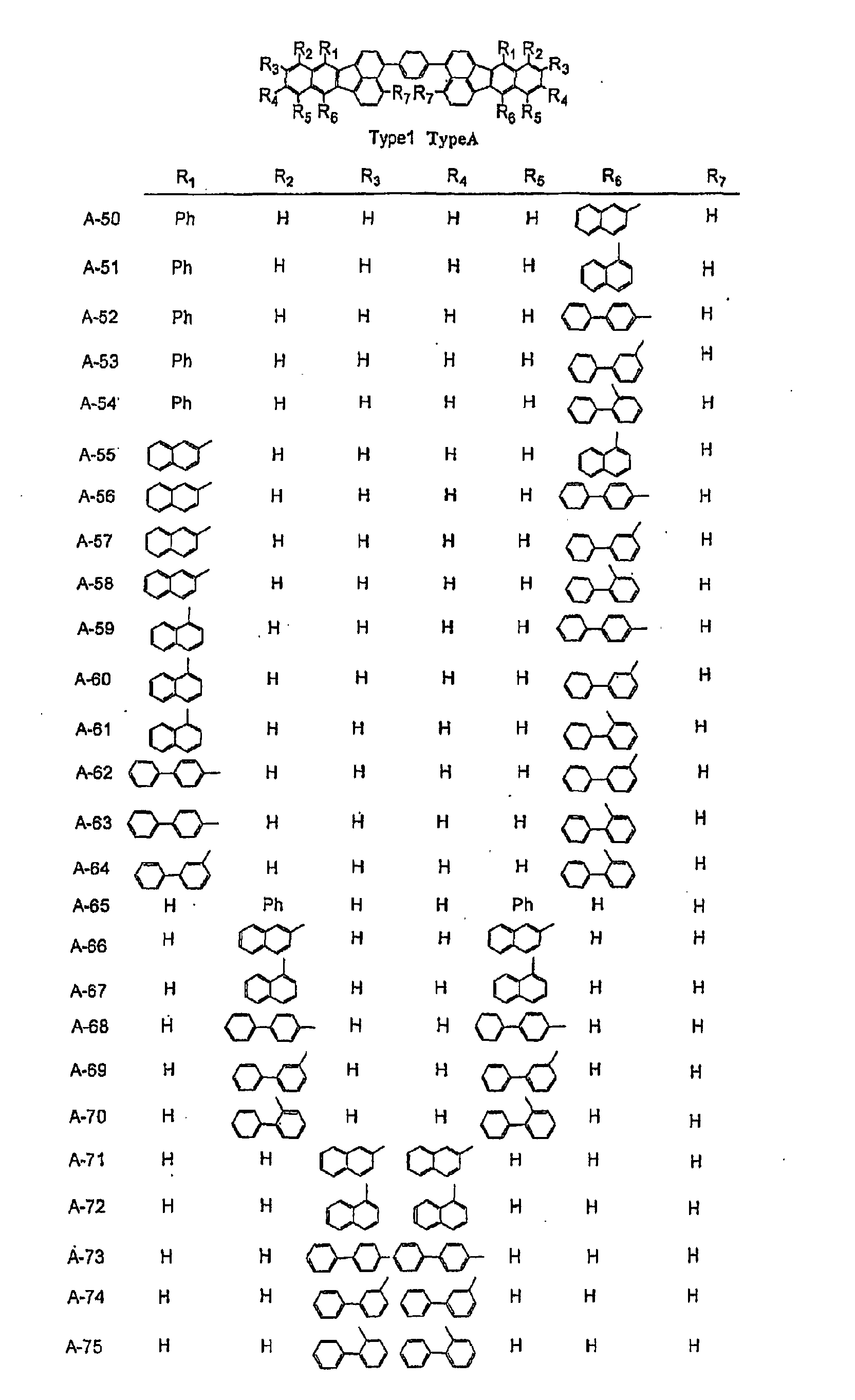
- the anthracene base host material and the inventive compound A-2 as the dopant both of the structures shown below, were evaporated in a weight ratio of 98:2 and at an overall deposition rate of 0.1 nm/sec to a thickness of 40 nm, forming a light emitting layer.
- tris(8-hydroxyquinoline)-aluminum (Alq3) was evaporated at a deposition rate of 0.1 nm/sec to a thickness of 15 nm, forming an electron injecting and transporting layer.
- LiF was evaporated at a deposition rate of 0.1 nm/sec to a thickness of 0.5 nm, forming an electron injecting electrode.
- Aluminum was evaporated to a thickness of 100 nm to form a protective electrode.
- Final glass sealing completed an organic EL device.
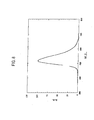
- a DC voltage was applied across the organic EL device. Initially, the device was found to produce light emission to a luminance of at least 730 cd/m 2 when operated at a current density of 10 mA/cm 2 and a drive voltage of 8.6 volts. At this point, the peak wavelength was 450 nm and the chromaticity coordinates (x, y) were (0.15, 0.11). When the device was continuously driven by conducting a constant current of 10 mA/cm 2 , it exhibited a luminance half-life period of at least 500 hours from the initial luminance of at least 730 cd/m 2 . Therefore, the luminance (cd) multiplied by the half-life period (h) was 365,000. The spectrum of light emission is shown in FIG. 5.
- Example 1 N,N'-diphenyl-N,N'-bis[N-(4-methylphenyl)-N-phenyl-(4-aminophenyl)]-1,1'-biphenyl-4,4'-diamine was evaporated at a deposition rate of 0.1 nm/sec. to a thickness of 50 nm, forming a hole injecting layer.
- N,N,N',N'-tetrakis(m-biphenyl)-1,1'-biphenyl-4,4'-diamine as the host material and the inventive compound A-2 as the dopant were evaporated in a weight ratio of 98:2 and at an overall deposition rate of 0.1 nm/sec to a thickness of 30 nm, forming a hole transporting and light emitting layer.
- tris(8-hydroxyquinoline)-aluminum (Alq3) was evaporated at a deposition rate of 0.1 nm/sec to a thickness of 40 nm, forming an electron injecting and transporting layer.
- LiF was evaporated at a deposition rate of 0.1 nm/sec to a thickness of 0.3 nm, forming an electron injecting electrode.
- Aluminum was evaporated to a thickness of 200 nm to form a protective electrode.
- Final glass sealing completed an organic EL device.
- a DC voltage was applied across the organic EL device. Initially, the device was found to produce light emission to a luminance of at least 780 cd/m 2 when operated at a current density of 10 mA/cm 2 and a drive voltage of 7.9 volts. At this point, the peak wavelength was 450 nm and the chromaticity coordinates (x, y) were (0.15, 0.11). When the device was continuously driven by conducting a constant current of 10 mA/cm 2 , it exhibited a luminance half-life period of at least 400 hours from the initial luminance of at least 780 cd/m 2 .
- Example 1 N,N'-diphenyl-N,N'-bis[N-(4-methylphenyl)-N-phenyl-(4-aminophenyl)]-1,1'-biphenyl-4,4'-diamine was evaporated at a deposition rate of 0.1 nm/sec. to a thickness of 50 nm, forming a hole injecting layer.
- N,N,N',N'-tetrakis(m-biphenyl)-1,1'-biphenyl-4,4'-diamine was evaporated at a deposition rate of 0.1 nm/sec to a thickness of 20 nm, forming a hole transporting layer.
- the inventive compound A-2 of Example 1 as the host material and a naphthacene base compound of the structures shown below as the dopant were evaporated in a weight ratio of 98:2 and at an overall deposition rate of 0.1 nm/sec to a thickness of 40 nm, forming a light emitting layer.
- tris(8-hydroxyquinoline)-aluminum (Alq3) was evaporated at a deposition rate of 0.1 nm/sec to a thickness of 30 nm, forming an electron injecting and transporting layer.
- LiF was evaporated at a deposition rate of 0.1 nm/sec to a thickness of 0.3 nm, forming an electron injecting electrode.
- Aluminum was evaporated to a thickness of 150 nm to form a protective electrode.
- Final glass sealing completed an organic EL device.
- a DC voltage was applied across the organic EL device. Initially, the device was found to produce light emission to a luminance of at least 900 cd/m 2 when operated at a current density of 10 mA/cm 2 and a drive voltage of 6.3 volts. At this point, the peak wavelength was 560 nm and the chromaticity coordinates (x, y) were (0.45, 0.55). When the device was continuously driven by conducting a constant current of 10 mA/cm 2 , it exhibited a luminance half-life period of at least 3,000 hours from the initial luminance of at least 900 cd/m 2 .
- An organic EL device was fabricated as in Example 3 except that the dopant used in the light emitting layer in Example 3 was replaced by a naphthacene base compound of the structure shown below.
- a DC voltage was applied across the organic EL device. Initially, the device was found to produce light emission to a luminance of at least 910 cd/m 2 when operated at a current density of 10 mA/cm 2 and a drive voltage of 6.3 volts. At this point, the peak wavelength was 560 nm and the chromaticity coordinates (x, y) were (0.45, 0.55). When the device was continuously driven by conducting a constant current of 10 mA/cm 2 , it exhibited a luminance half-life period of at least 3,000 hours from the initial luminance of at least 910 cd/m 2 .
- Example 3 An organic EL device was fabricated as in Example 3 except that the dopant used in the light emitting layer in Example 3 was replaced by a compound of the structure shown below.
- a DC voltage was applied across the organic EL device. Initially, the device was found to produce light emission to a luminance of at least 750 cd/m 2 when operated at a current density of 10 mA/cm 2 and a drive voltage of 6.5 volts. At this point, the peak wavelength was 580 nm and the chromaticity coordinates (x, y) were (0.52, 0.48). When the device was continuously driven by conducting a constant current of 10 mA/cm 2 , it exhibited a luminance half-life period of at least 3 , 000 hours from the initial luminance of at least 750 cd/m 2 .
- Example 3 An organic EL device was fabricated as in Example 3 except that the dopant used in the light emitting layer in Example 3 was replaced by a compound of the structure shown below.
- a DC voltage was applied across the organic EL device. Initially, the device was found to produce light emission to a luminance of at least 1100 cd/m 2 when operated at a current density of 10 mA/cm 2 and a drive voltage of 6.6 volts. At this point, the peak wavelength was 515 nm and the chromaticity coordinates (x, y) were (0.30, 0.65). When the device was continuously driven by conducting a constant current of 10 mA/cm 2 , it exhibited a luminance half-life period of at least 3,000 hours from the initial luminance of at least 1100 cd/m 2 .
- Example 3 An organic EL device was fabricated as in Example 3 except that the dopant used in Example 3 was replaced by a compound of the structure shown below.
- a DC voltage was applied across the organic EL device. Initially, the device was found to produce light emission to a luminance of at least 550 cd/m 2 when operated at a current density of 10 mA/cm 2 and a drive voltage of 6.5 volts. At this point, the peak wavelength was 610 nm and the chromaticity coordinates (x, y) were (0.65, 0.35). When the device was continuously driven by conducting a constant current of 10 mA/cm 2 , it exhibited a luminance half-life period of at least 5, 000 hours from the initial luminance of at least 550 cd/m 2 .
- Example 1 N,N'-diphenyl-N,N'-bis[N-(4-methylphenyl)-N-phenyl-(4-aminophenyl)]-1,1'-biphenyl-4,4'-diamine was evaporated at a deposition rate of 0.1 nm/sec. to a thickness of 50 nm, forming a hole injecting layer.
- N,N,N',N'-tetrakis(m-biphenyl)-1,1'-biphenyl-4,4'-diamine was evaporated at a deposition rate of 0.1 nm/sec to a thickness of 20 nm, forming a first hole transporting layer.
- the inventive compound A-2 of Example 1 was evaporated at a deposition rate of 0.1 nm/sec to a thickness of 10 nm, forming a second hole transporting layer.
- a compound of the following structure as the host material and a compound of the following structure: as the dopant were evaporated in a weight ratio of 98:2 and at an overall deposition rate of 0.1 nm/sec to a thickness of 40 nm, forming a light emitting layer.
- tris(8-hydroxyquinoline)-aluminum (Alq3) was evaporated at a deposition rate of 0.1 nm/sec to a thickness of 30 nm, forming an electron injecting and transporting layer.
- LiF was evaporated at a deposition rate of 0.1 nm/sec to a thickness of 0.3 nm, forming an electron injecting electrode.
- Aluminum was evaporated to a thickness of 150 nm to form a protective electrode.
- Final glass sealing completed an organic EL device.
- a DC voltage was applied across the organic EL device. Initially, the device was found to produce light emission to a luminance of at least 820 cd/m 2 when operated at a current density of 10 mA/cm 2 and a drive voltage of 6.0 volts. At this point, the peak wavelength was 556 nm and the chromaticity coordinates (x, y) were (0.45, 0.55).
- Example 1 N,N'-diphenyl-N,N'-bis[N-(4-methylphenyl)-N-phenyl-(4-aminophenyl)]-1,1'-biphenyl-4,4'-diamine was evaporated at a deposition rate of 0.1 nm/sec. to a thickness of 90 nm, forming a hole injecting layer.
- N,N,N',N'-tetrakis(m-biphenyl)-1,1'-biphenyl-4,4'-diamine was evaporated at a deposition rate of 0.1 nm/sec to a thickness of 10 nm, forming a hole transporting layer.
- the inventive compound A-2 was evaporated at a deposition rate of 0.1 nm/sec to a thickness of 10 nm, forming a second hole transporting layer.
- Example 8 the compound used in Example 8 as the host material and the inventive compound A-2 as the dopant were evaporated in a weight ratio of 98:2 and at an overall deposition rate of 0.1 nm/sec to a thickness of 40 nm, forming a light emitting layer.
- tris(8-hydroxyquinoline)-aluminum (Alq3) was evaporated at a deposition rate of 0.1 nm/sec to a thickness of 15 nm, forming an electron injecting and transporting layer.
- LiF was evaporated at a deposition rate of 0.1 nm/sec to a thickness of 0.5 nm, forming an electron injecting electrode.
- Aluminum was evaporated to a thickness of 100 nm to form a protective electrode.
- Final glass sealing completed an organic EL device.
- a DC voltage was applied across the organic EL device. Initially, the device was found to produce light emission to a luminance of at least 700 cd/m 2 when operated at a current density of 10 mA/cm 2 and a drive voltage of 8.0 volts. At this point, the peak wavelength was 450 nm and the chromaticity coordinates (x, y) were (0.15, 0.11). When the device was continuously driven by conducting a constant current of 10 mA/cm 2 , it exhibited a luminance half-life period of at least 1,000 hours from the initial luminance of at least 700 cd/m 2 .
- Example 1 N,N'-diphenyl-N,N'-bis[N-(4-methylphenyl)-N-phenyl-(4-aminophenyl)]-1,1'-biphenyl-4,4'-diamine was evaporated at a deposition rate of 0.1 nm/sec. to a thickness of 10 nm, forming a hole injecting layer.
- N,N,N',N'-tetrakis(m-biphenyl)-1,1'-biphenyl-4,4'-diamine was evaporated at a deposition rate of 0.1 nm/sec to a thickness of 20 nm, forming a hole transporting layer.
- N,N,N',N'-tetrakis(m-biphenyl)-1,1'-biphenyl-4,4'-diamine, the compound of [C70], and the compound of [C69] as the dopant were evaporated in a weight ratio of 49:49:2 and at an overall deposition rate of 0.1 nm/sec to a thickness of 15 nm, forming a first (red) light emitting layer.
- N,N,N',N'-tetrakis(m-biphenyl)-1,1'-biphenyl-4,4'-diamine, the compound of [C70], and the compound of [C68] as the dopant were evaporated in a weight ratio of 49:49:2 and at an overall deposition rate of 0.1 nm/sec to a thickness of 20 nm, forming a second (green) light emitting layer.
- N,N,N',N'-tetrakis(m-biphenyl)-1,1'-biphenyl-4,4'-diamine, the compound of [C70], and the inventive compound A-2 as the dopant were evaporated in a weight ratio of 49:49:2 and at an overall deposition rate of 0.1 nm/sec to a thickness of 20 nm, forming a second (blue) light emitting layer.
- Example 2 Otherwise as in Example 1, an organic EL device was fabricated.
- a DC voltage was applied across the organic EL device. Initially, the device was found to produce light emission to a luminance of at least 750 cd/m 2 when operated at a current density of 10 mA/cm 2 and a drive voltage of 8.5 volts.
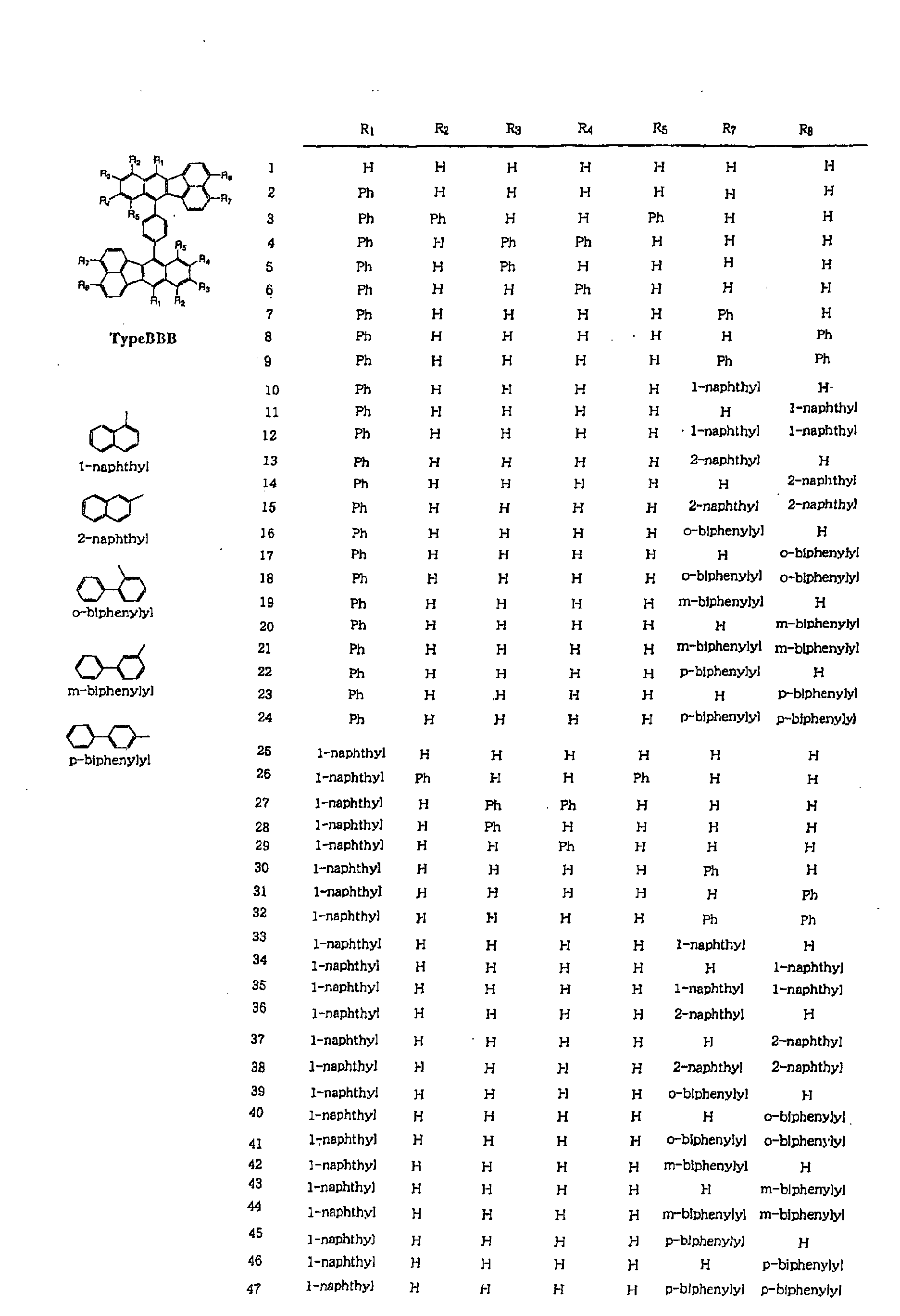
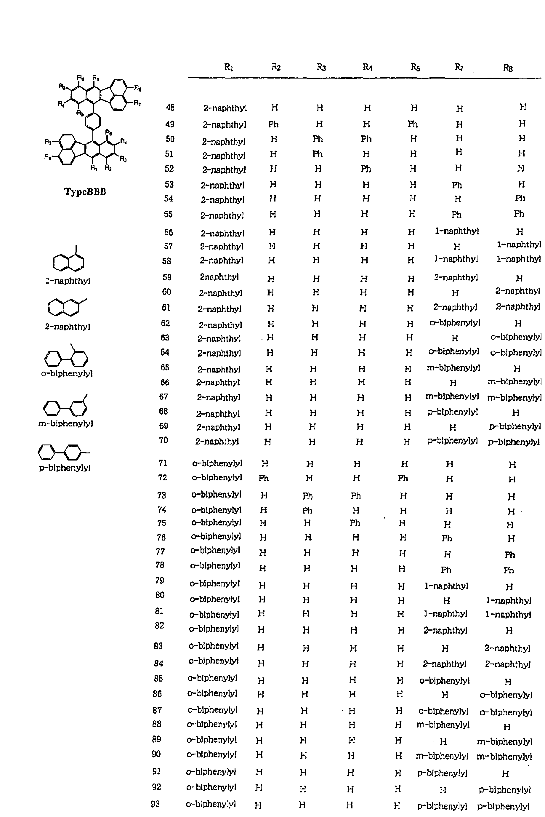
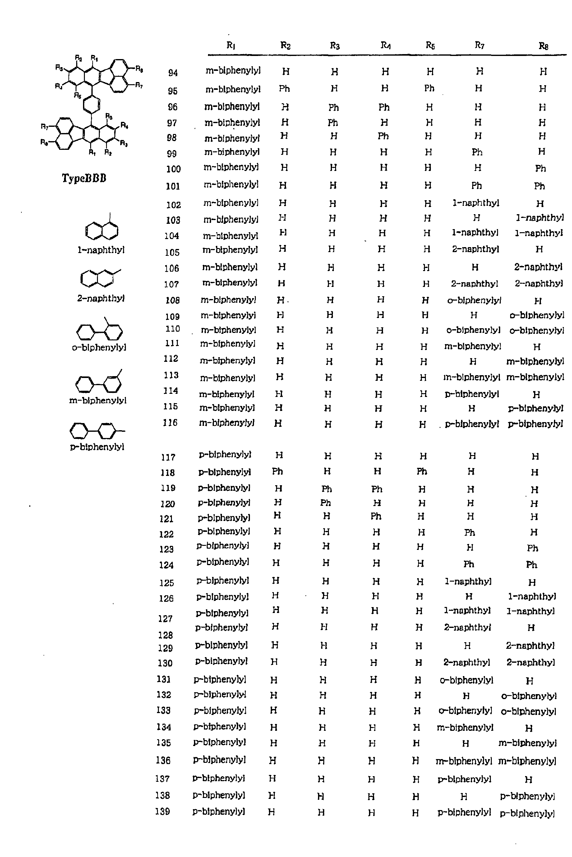
- Example 1 An organic EL device was fabricated as in Example 1 except that the dopant used in the light emitting layer in Example 1 was replaced by a compound of the structure (Type BBB-9) shown below.
- a DC voltage was applied across the organic EL device. Initially, the device was found to produce light emission to a luminance of at least 800 cd/m 2 when operated at a current density of 10 mA/cm 2 and a drive voltage of 8.6 volts. At this point, the peak wavelength was 452 nm and the chromaticity coordinates (x, y) were (0.15, 0.11).
- the device When the device was continuously driven by conducting a constant current of 10 mA/cm 2 , it exhibited a luminance half-life period of at least 1,200 hours from the initial luminance of at least 800 cd/m 2 . Therefore, the luminance (cd) multiplied by the half-life period (h) was 960,000.
- the spectrum of light emission is shown in FIG. 6.
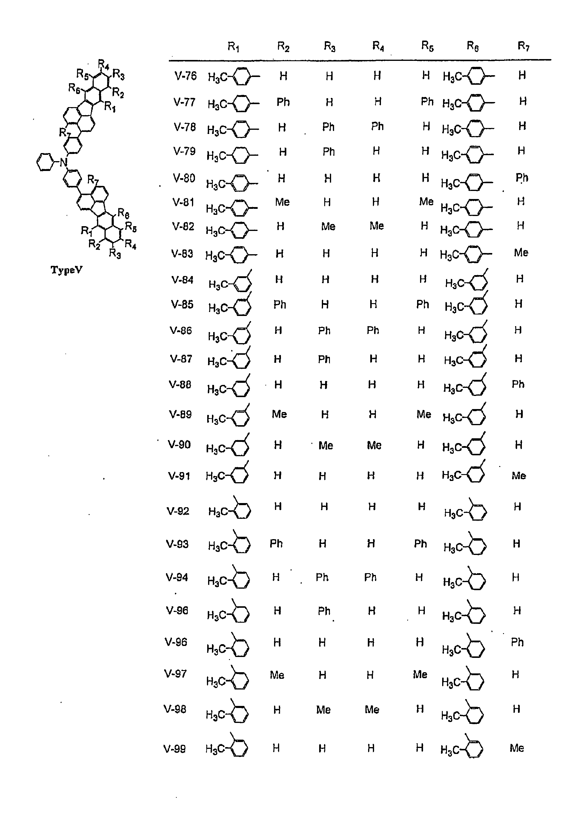
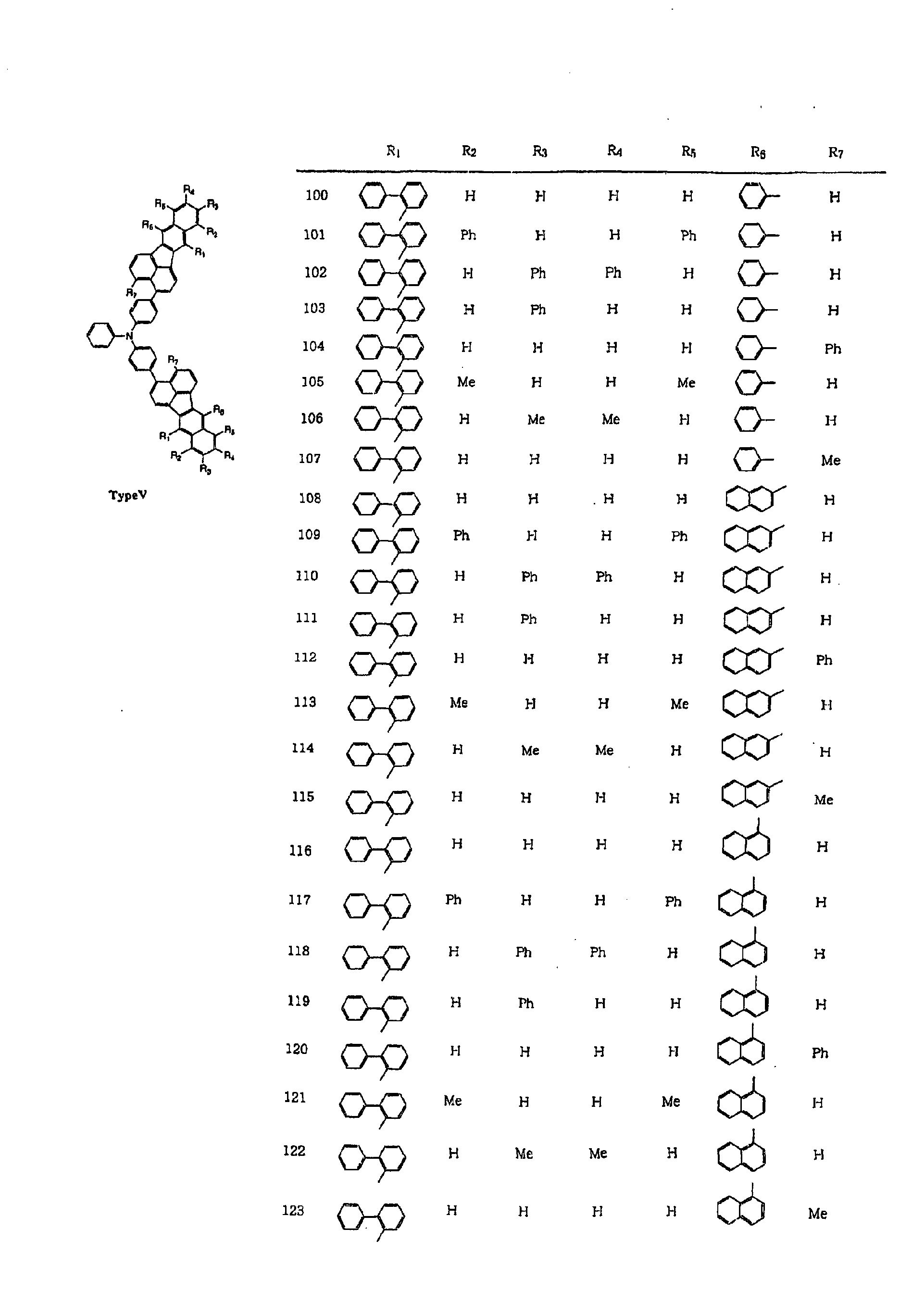
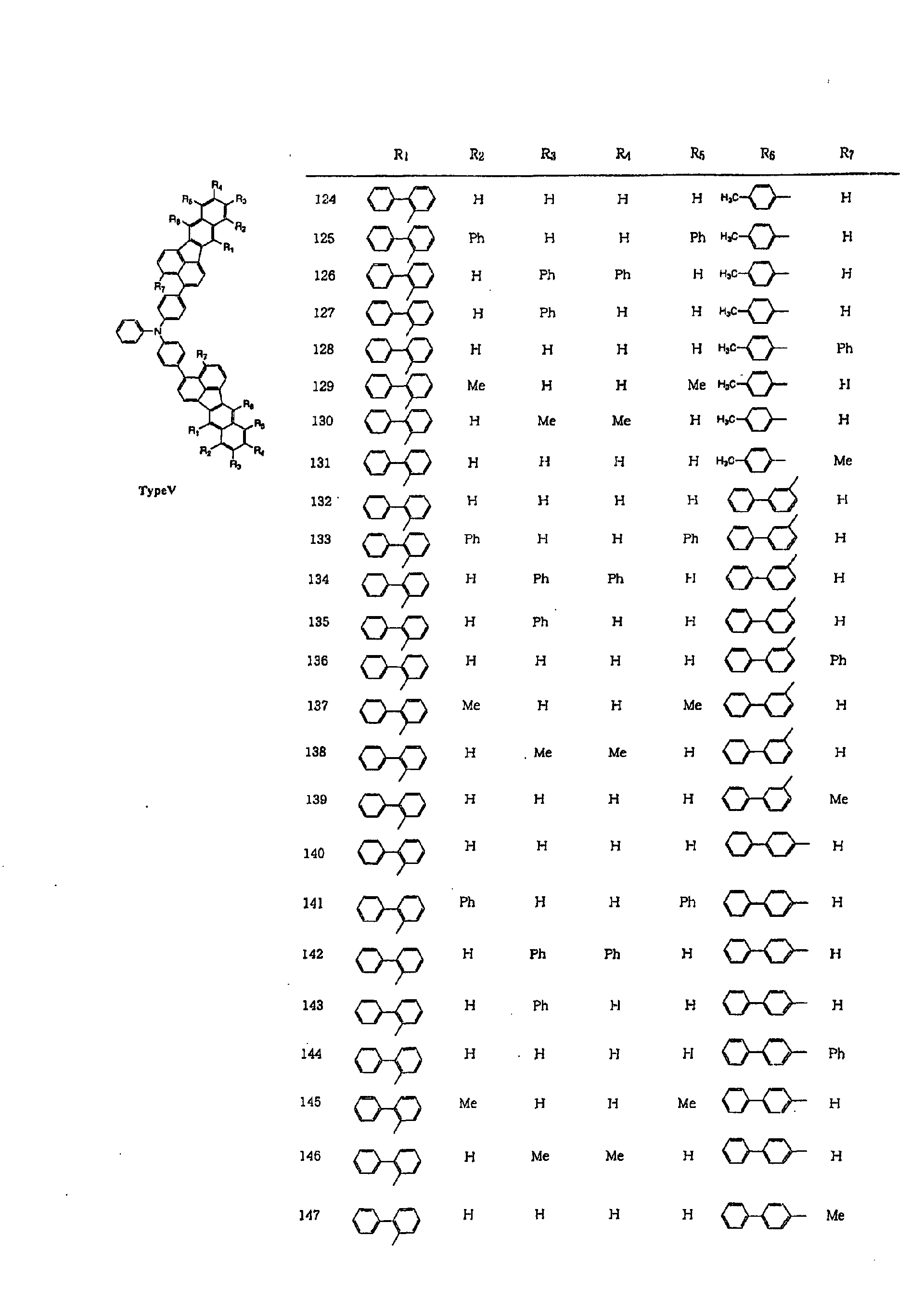
- Example 1 An organic EL device was fabricated as in Example 1 except that the dopant used in the light emitting layer in Example 1 was replaced by a compound of the structure (Type V-2) shown below.
- a DC voltage was applied across the organic EL device. Initially, the device was found to produce light emission to a luminance of at least 900 cd/m 2 when operated at a current density of 10 mA/cm 2 and a drive voltage of 8.6 volts. At this point, the peak wavelength was 473 nm and the chromaticity coordinates (x, y) were (0.14, 0.27).
- the device When the device was continuously driven by conducting a constant current of 50 mA/cm 2 , it exhibited an initial luminance of at least 4500 cd/m 2 and a luminance half-life period of at least 500 hours. Therefore, the luminance (cd) multiplied by the half-life period (h) was 22,500,000.
- the spectrum of light emission is shown in FIG. 7.
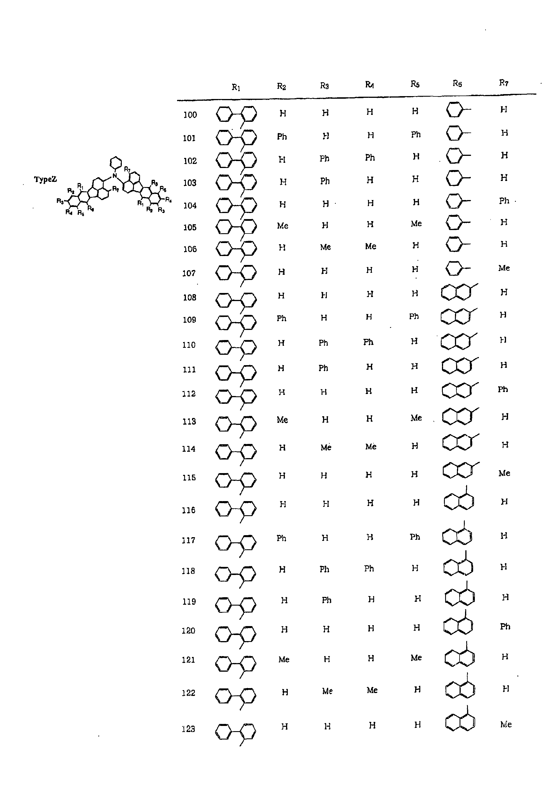
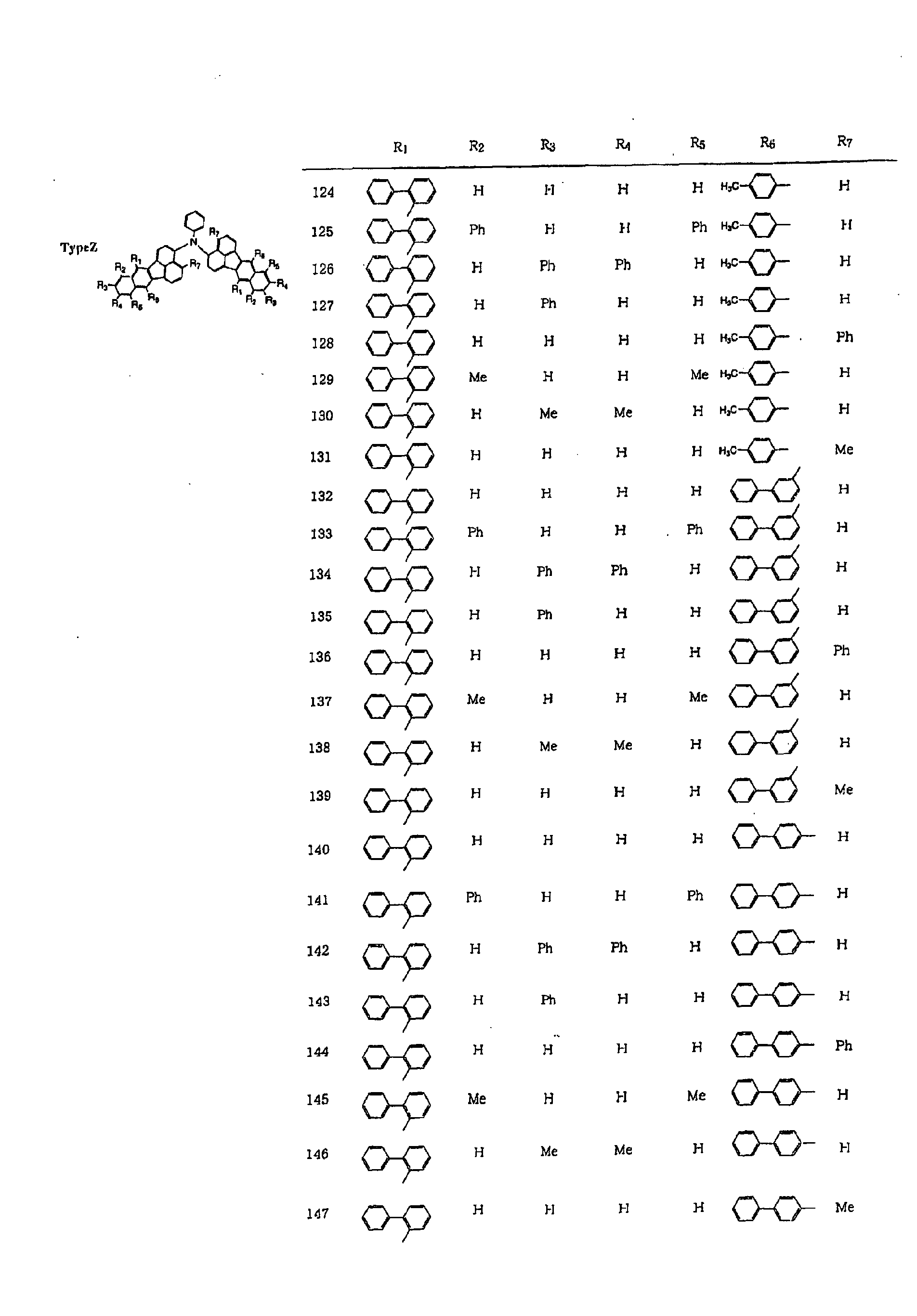
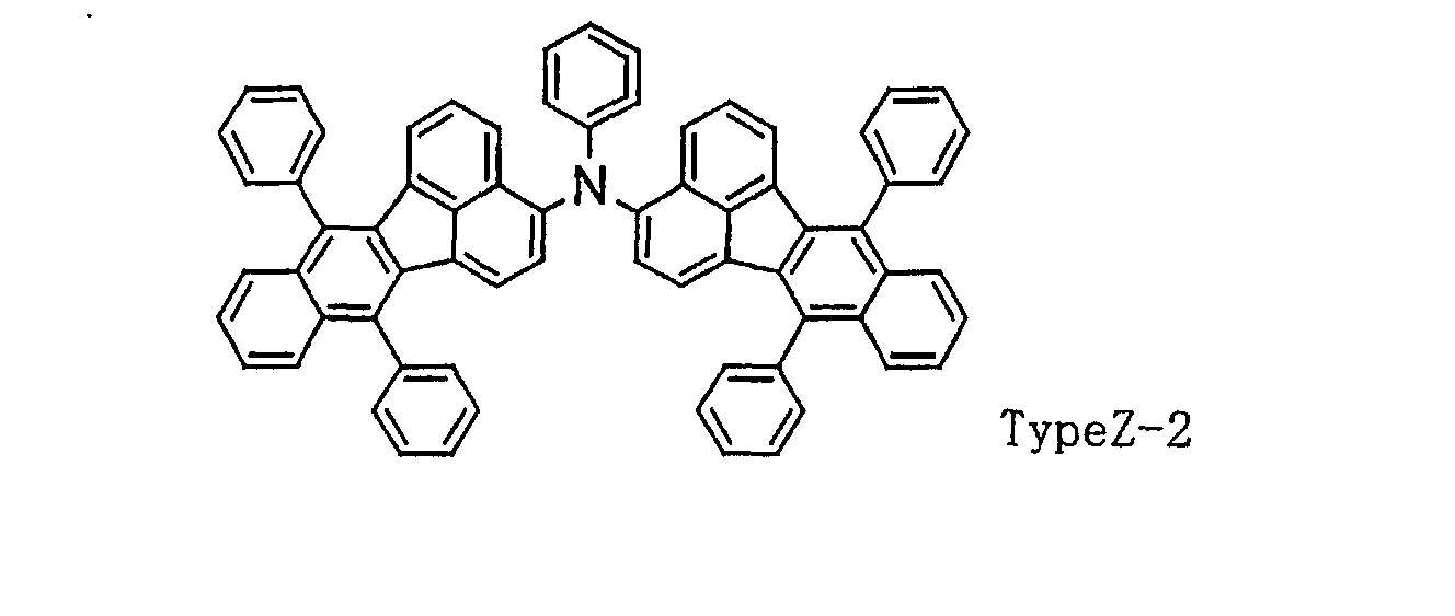
- Example 2 An organic EL device was fabricated as in Example 1 except that the dopant used in the light emitting layer in Example 1 was replaced by a compound of the structure (Type Z-2) shown below.
- a DC voltage was applied across the organic EL device. Initially, the device was found to produce light emission to a luminance of at least 1100 cd/m 2 when operated at a current density of 10 mA/cm 2 and a drive voltage of 8.6 volts. At this point, the peak wavelength was 518 nm and the chromaticity coordinates (x, y) were (0.28, 0.61).
- the device When the device was continuously driven by conducting a constant current of 50 mA/cm 2 , it exhibited an initial luminance of at least 5500 cd/m 2 and a luminance half-life period of at least 500 hours. Therefore, the luminance (cd) multiplied by the half-life period (h) was 27,500,000.
- the spectrum of light emission is shown in FIG. 8.
- An organic EL device was fabricated as in Example 1 except that the light emitting layer was not doped with the dopant.
- a DC voltage was applied across the organic EL device. Initially, the device was found to produce light emission to a luminance of up to 180 cd/m 2 when operated at a current density of 10 mA/cm 2 and a drive voltage of 6.5 volts. At this point, the peak wavelength was 440 nm and the chromaticity coordinates (x, y) were (0.16, 0.07).
- the device was continuously driven by conducting a constant current of 10 mA/cm 2 , it exhibited a luminance half-life period of up to 250 hours from the initial luminance of 180 cd/m 2 . Therefore, the luminance (cd) multiplied by the half-life period (h) was 4,500.
- An organic EL device was fabricated as in Example 1 except that the dopant in the light emitting layer was replaced by a compound of the following structure.
- a DC voltage was applied across the organic EL device. Initially, the device was found to produce light emission to a luminance of 700 cd/m 2 when operated at a current density of 10 mA/cm 2 and a drive voltage of 6.6 volts. At this point, the peak wavelength was 465 nm and the chromaticity coordinates (x, y) were (0.20, 0.20), indicating that the color of light emission was shifted from blue toward a longer wavelength side. When the device was continuously driven by conducting a constant current of 10 mA/cm 2 , it exhibited a luminance half-life period of 500 hours from the initial luminance of 700 cd/m 2 .
- An organic EL device was fabricated as in Example 1 except that the dopant in the light emitting layer was replaced by a compound of the following structure.
- a DC voltage was applied across the organic EL device. Initially, the device was found to produce light emission to a luminance of 180 cd/m 2 when operated at a current density of 10 mA/cm 2 and a drive voltage of 6.5 volts. At this point, the peak wavelength was 440 nm and the chromaticity coordinates (x, y) were (0.16, 0.07). When the device was continuously driven by conducting a constant current of 10 mA/cm 2 , it exhibited a luminance half-life period of 250 hours from the initial luminance of 180 cd/m 2 .
- compounds for use in organic EL devices capable of light emission to a satisfactory luminance, especially at a long wavelength, and with a high color purity, especially a color purity sufficient for use in full color displays, and having a sufficient durability to sustain such improved light emission performance over a long time are provided as well as organic EL devices using the same.
Landscapes
- Chemical & Material Sciences (AREA)
- Organic Chemistry (AREA)
- Engineering & Computer Science (AREA)
- Materials Engineering (AREA)
- Physics & Mathematics (AREA)
- Spectroscopy & Molecular Physics (AREA)
- Electroluminescent Light Sources (AREA)
- Organic Low-Molecular-Weight Compounds And Preparation Thereof (AREA)
Abstract

Description






at least one of the organic layers containing one or more compound for use in organic EL devices according to any one of (1) to (22).




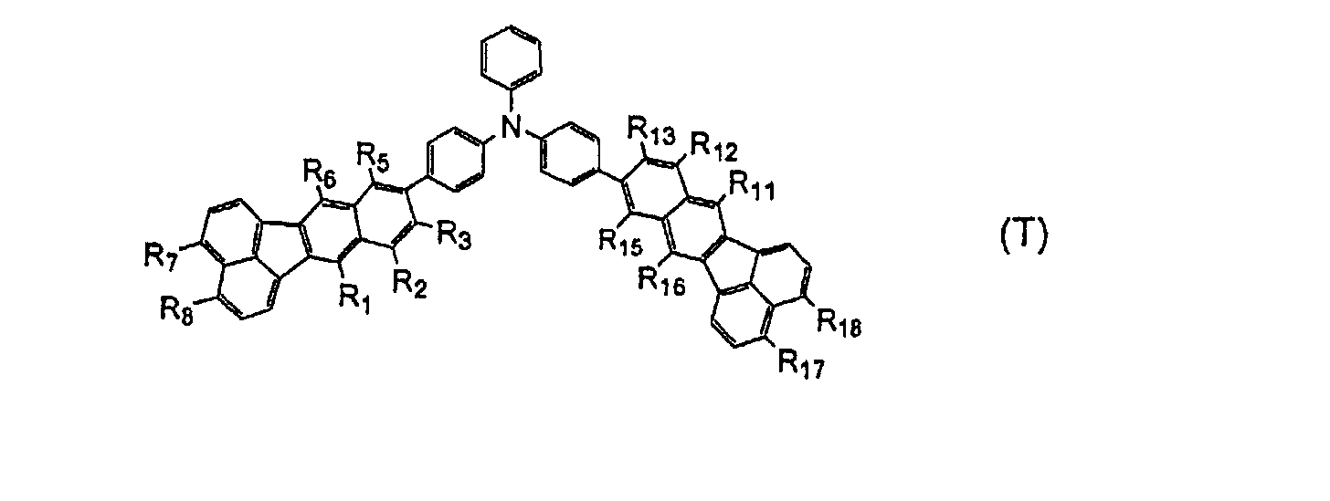
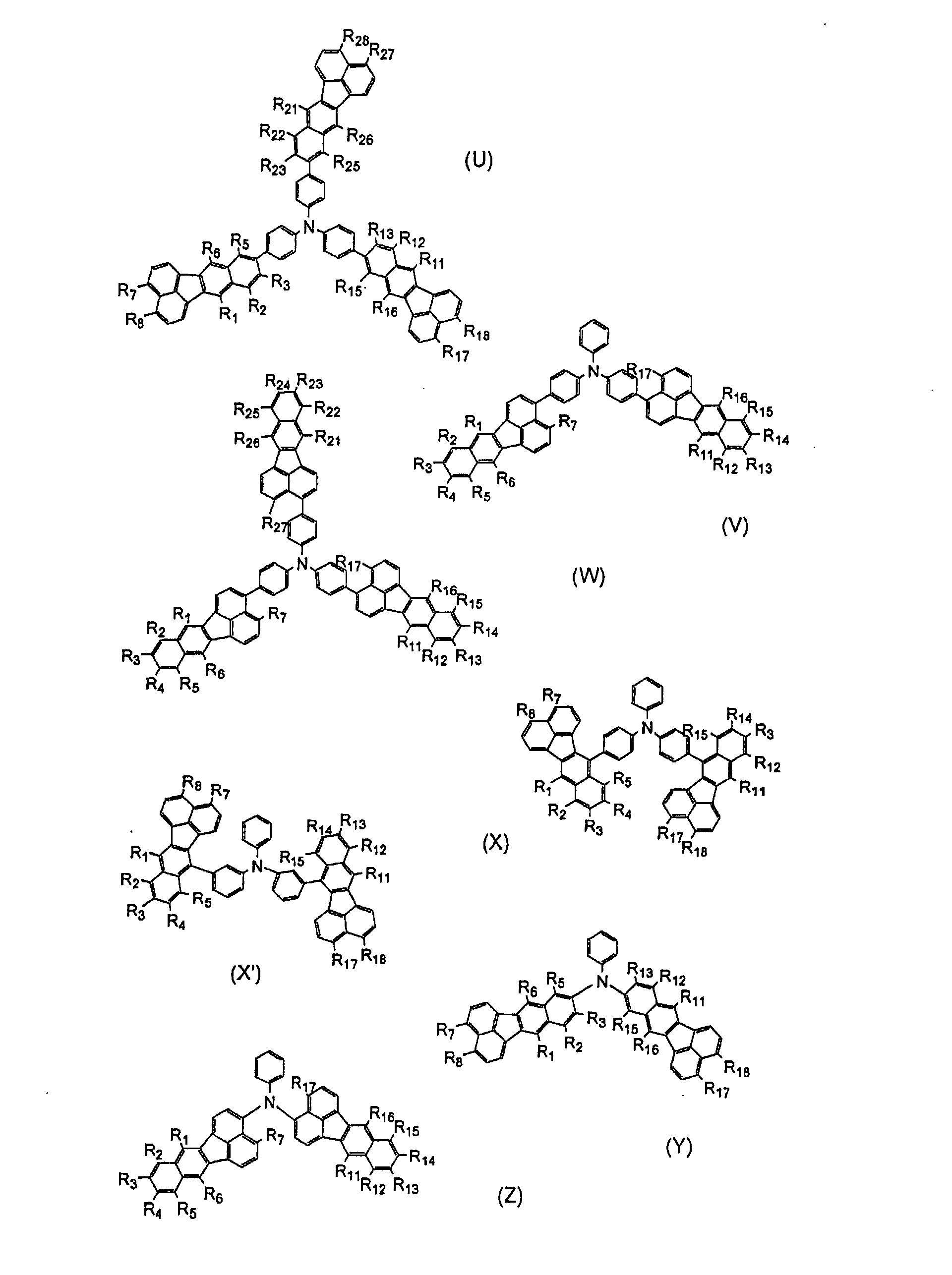


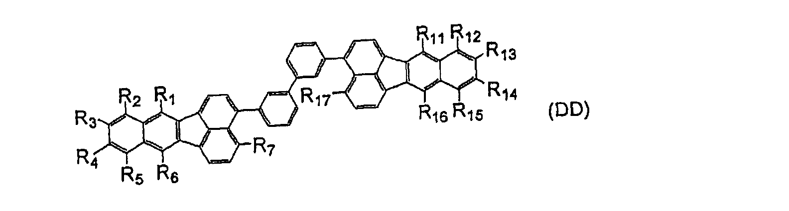
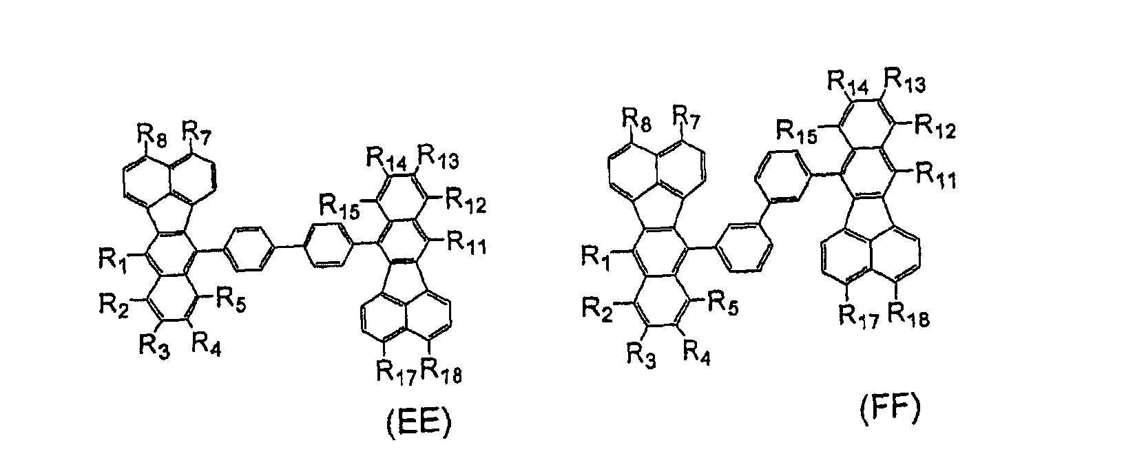











































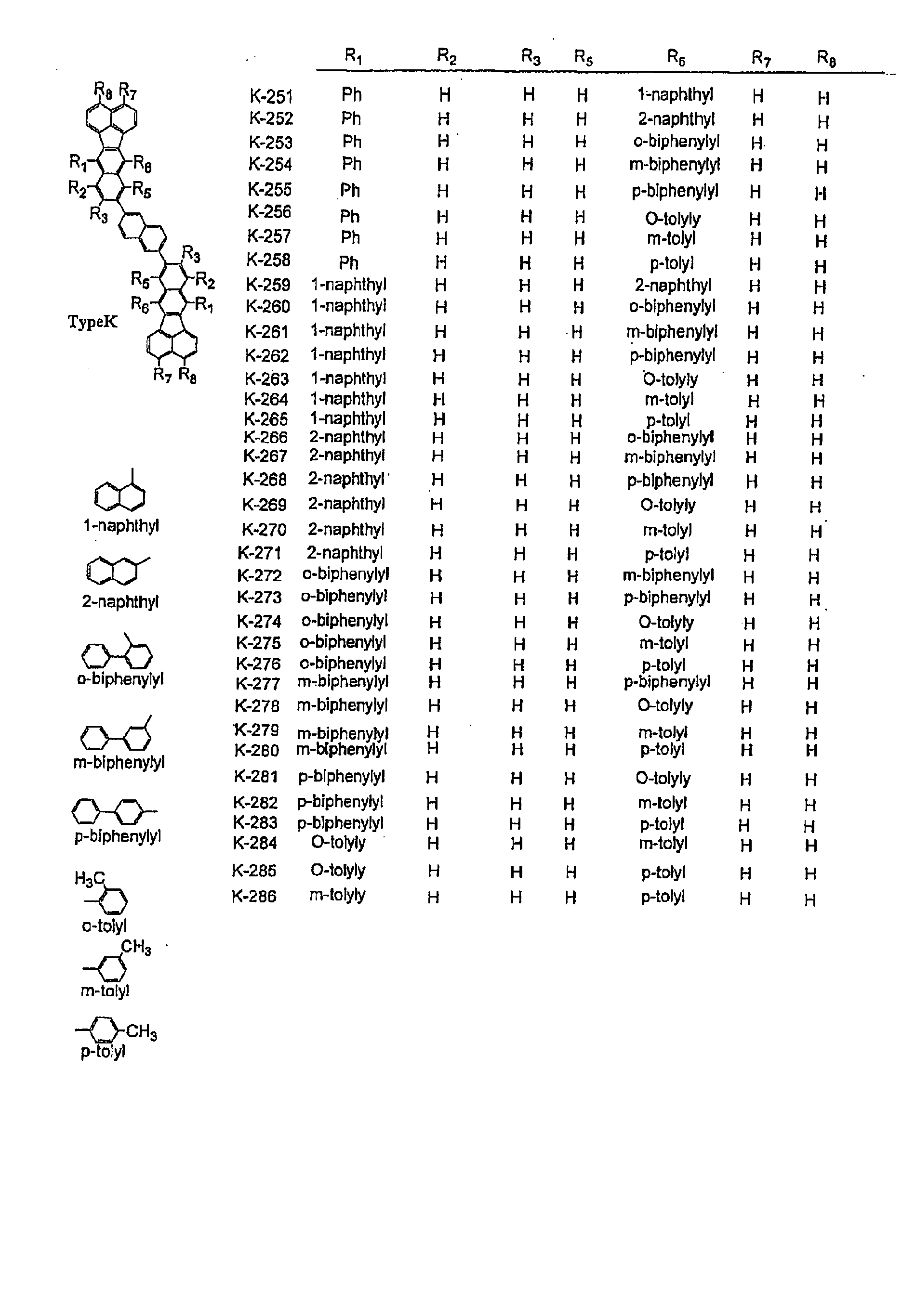
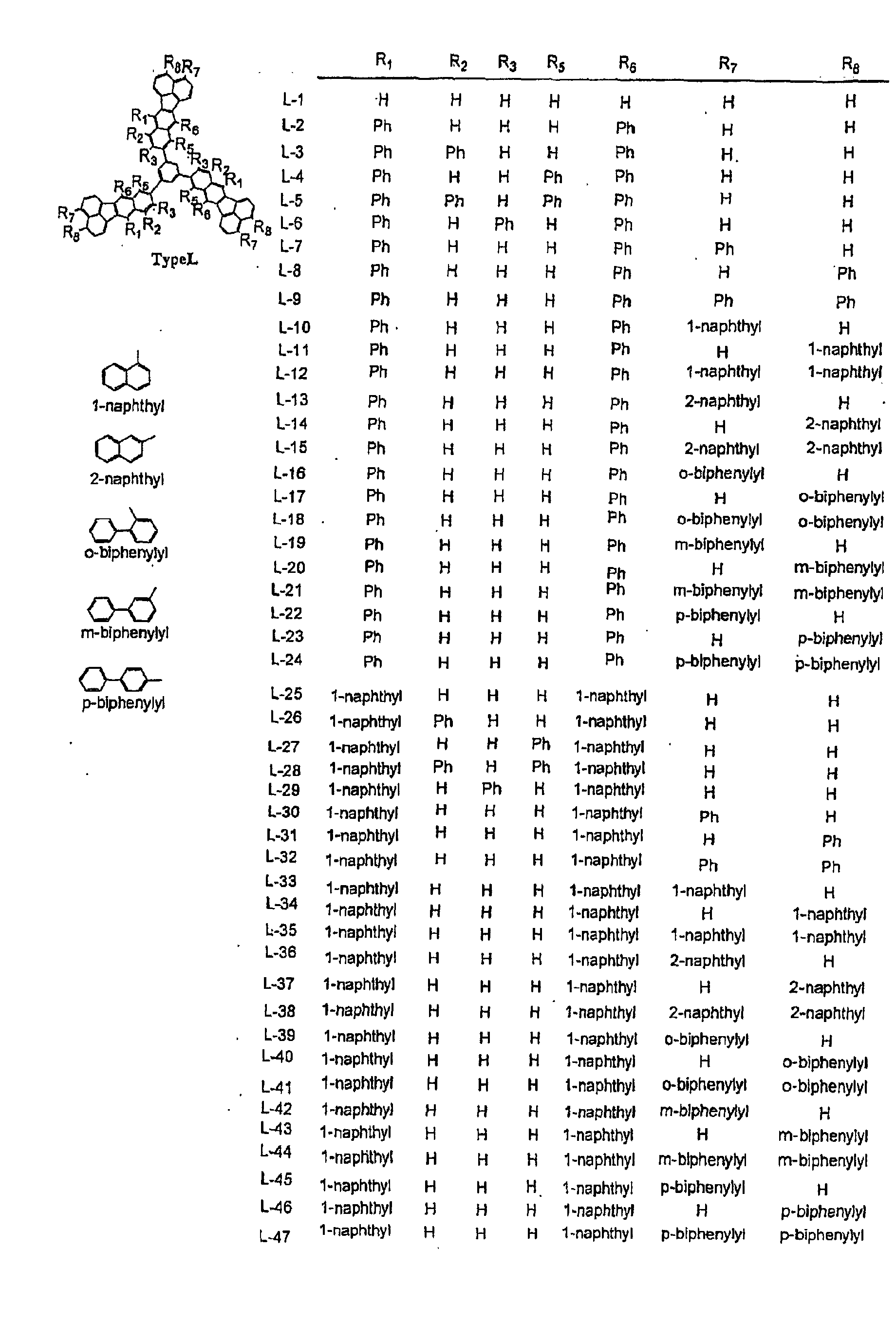
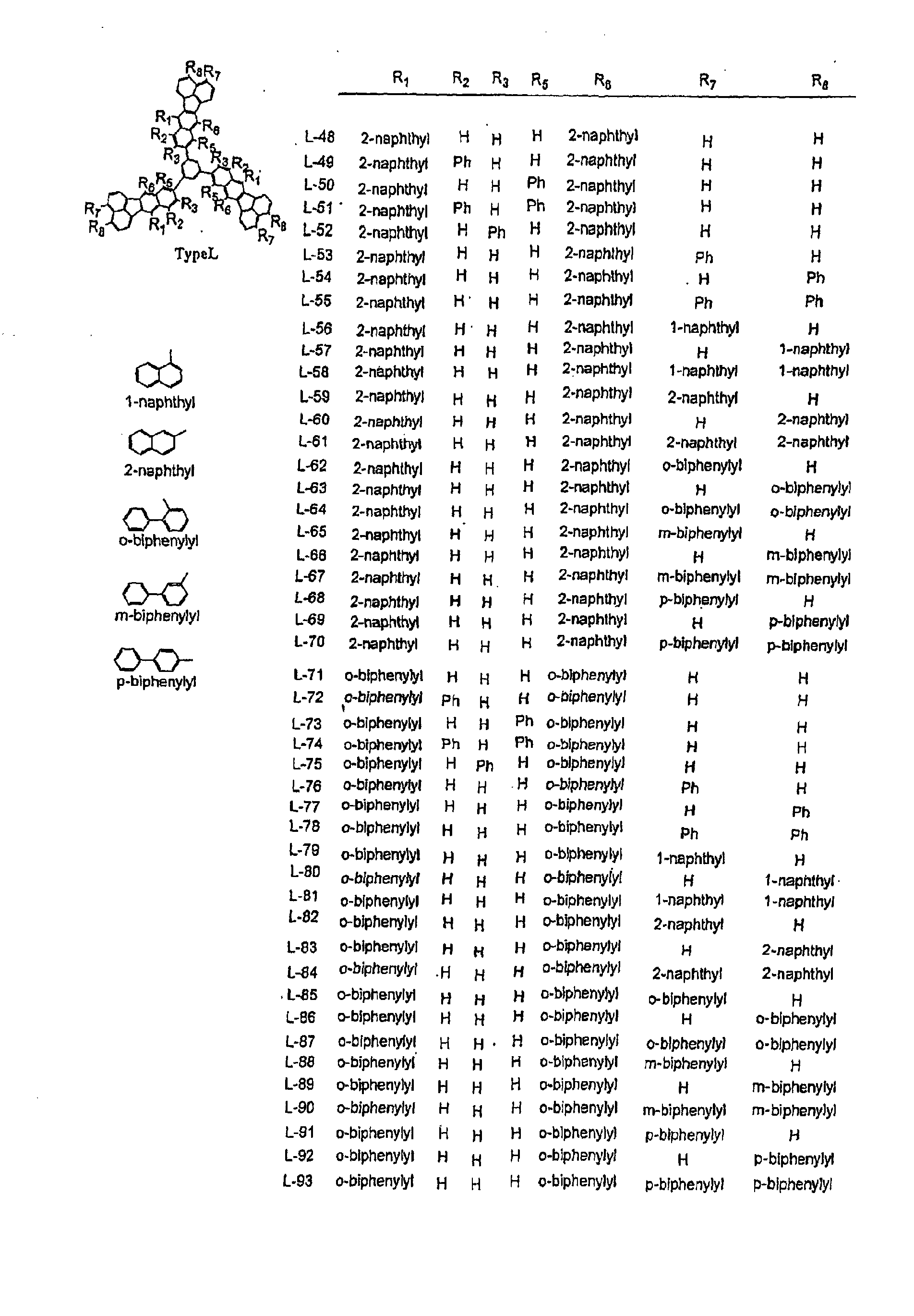


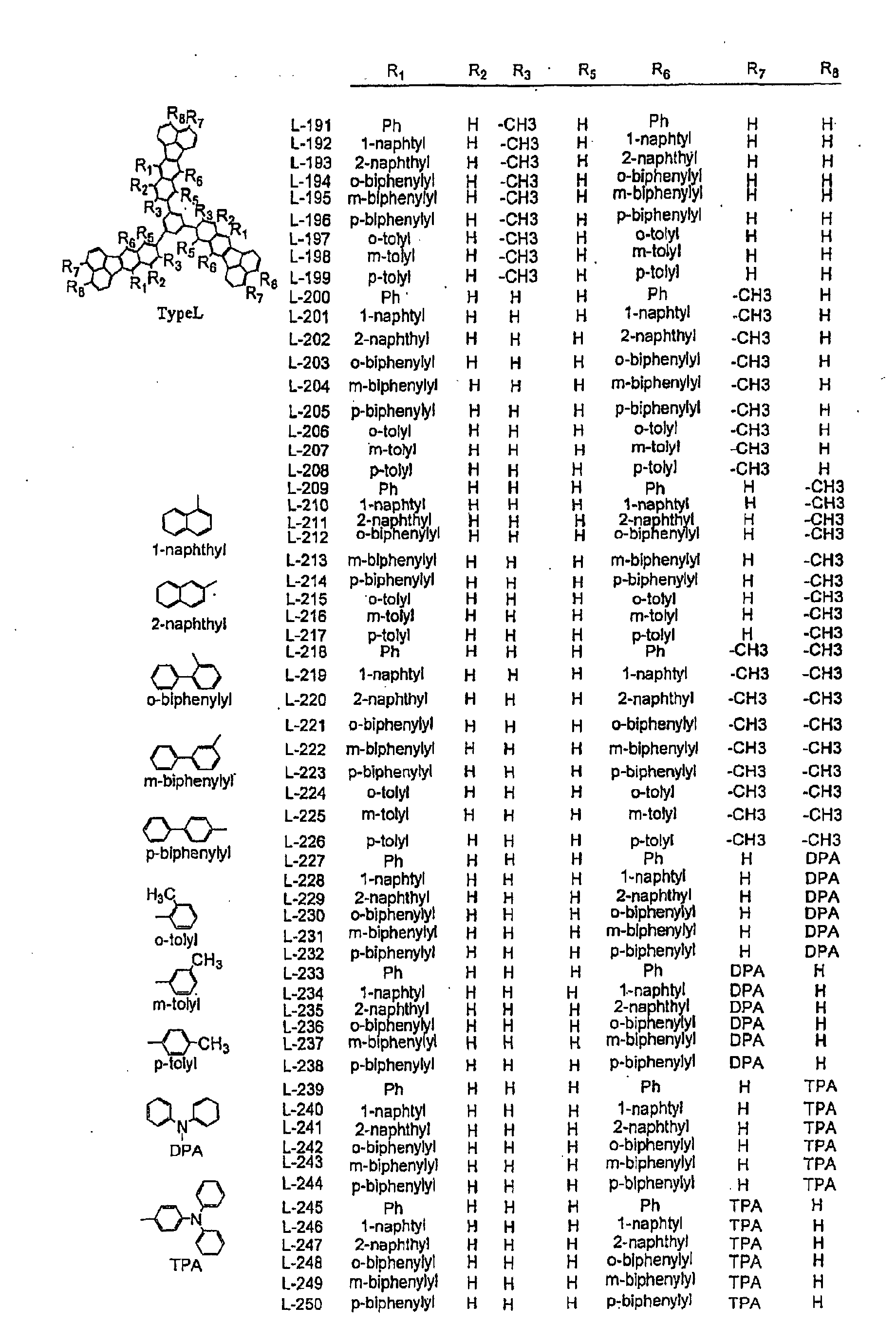




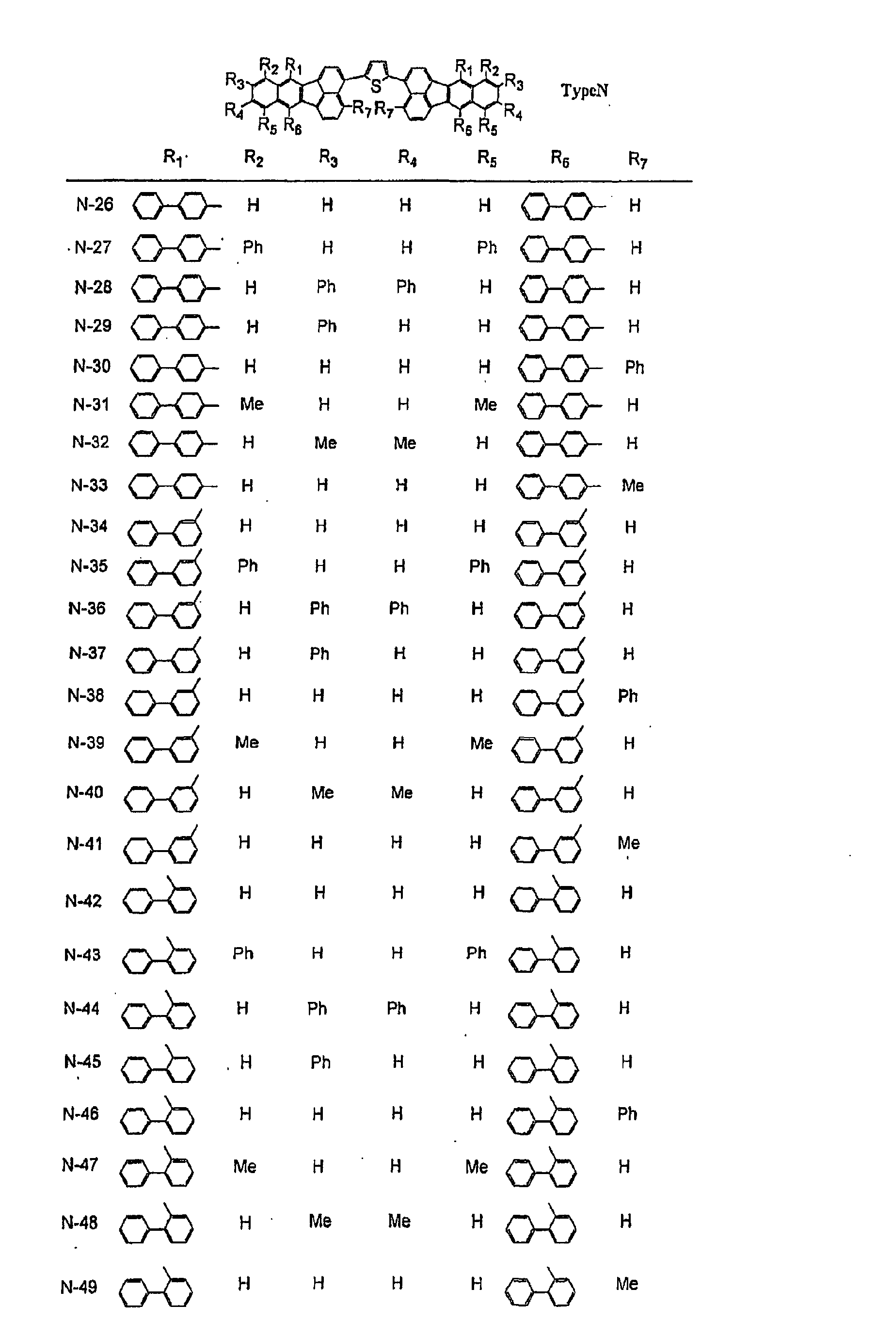

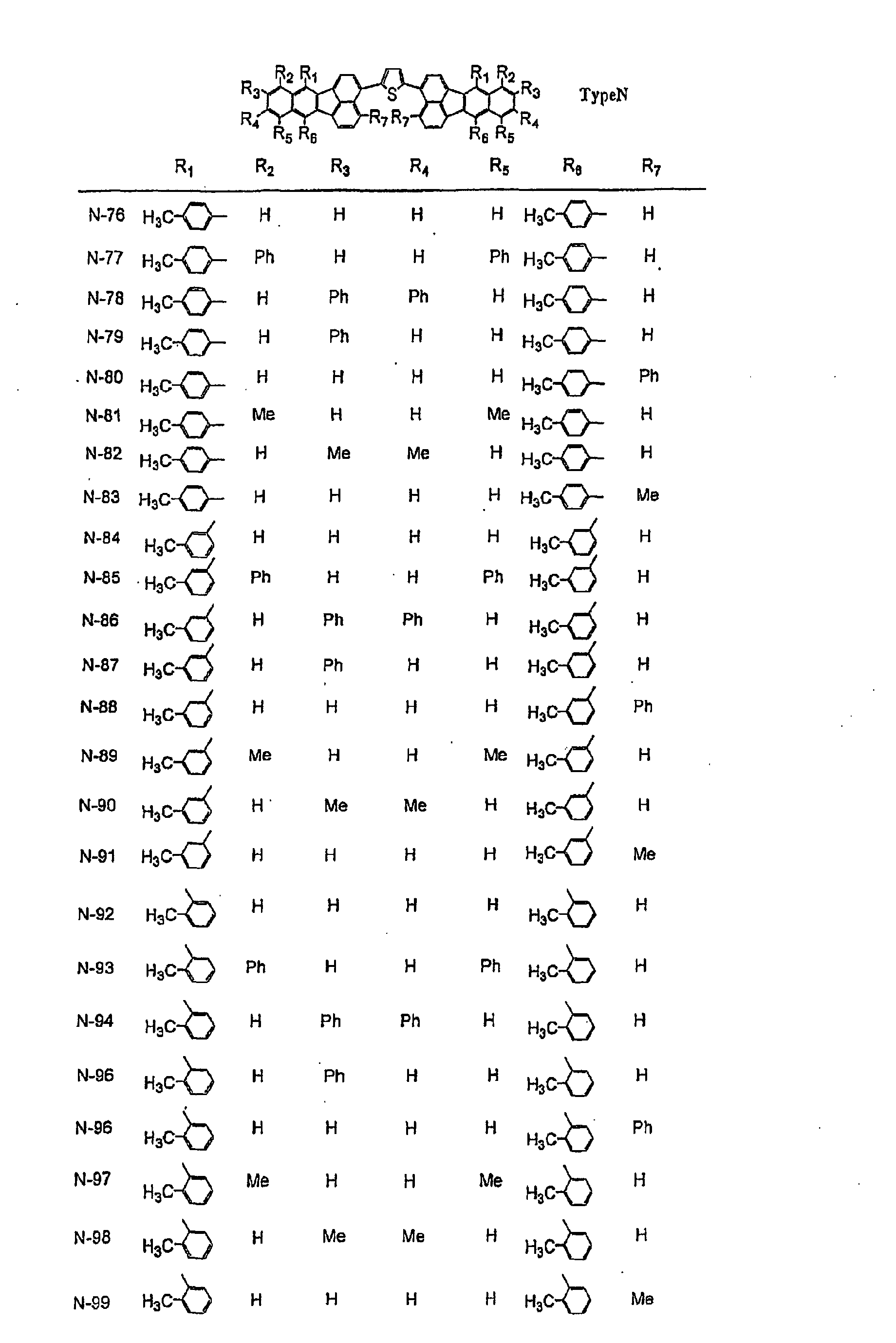


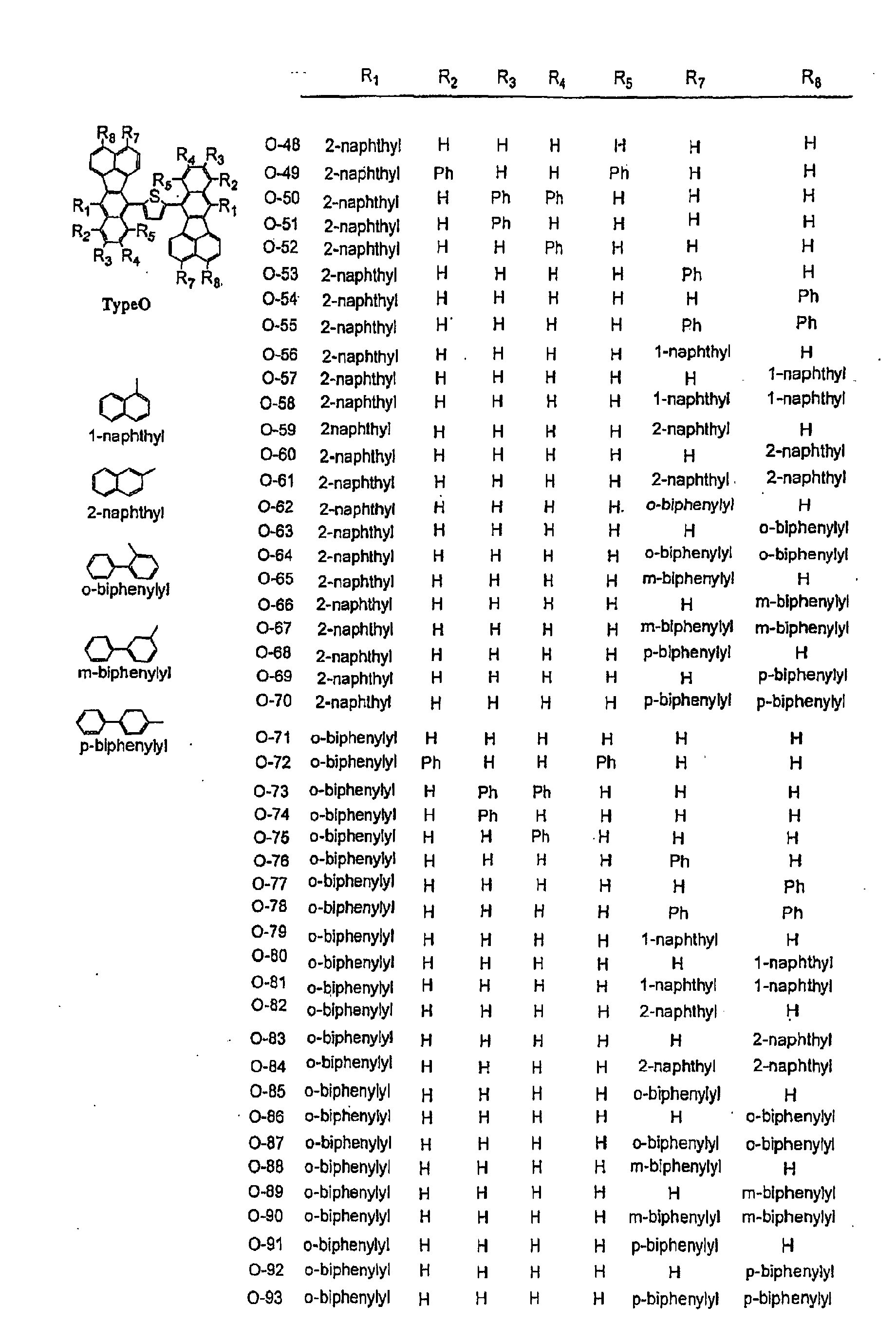

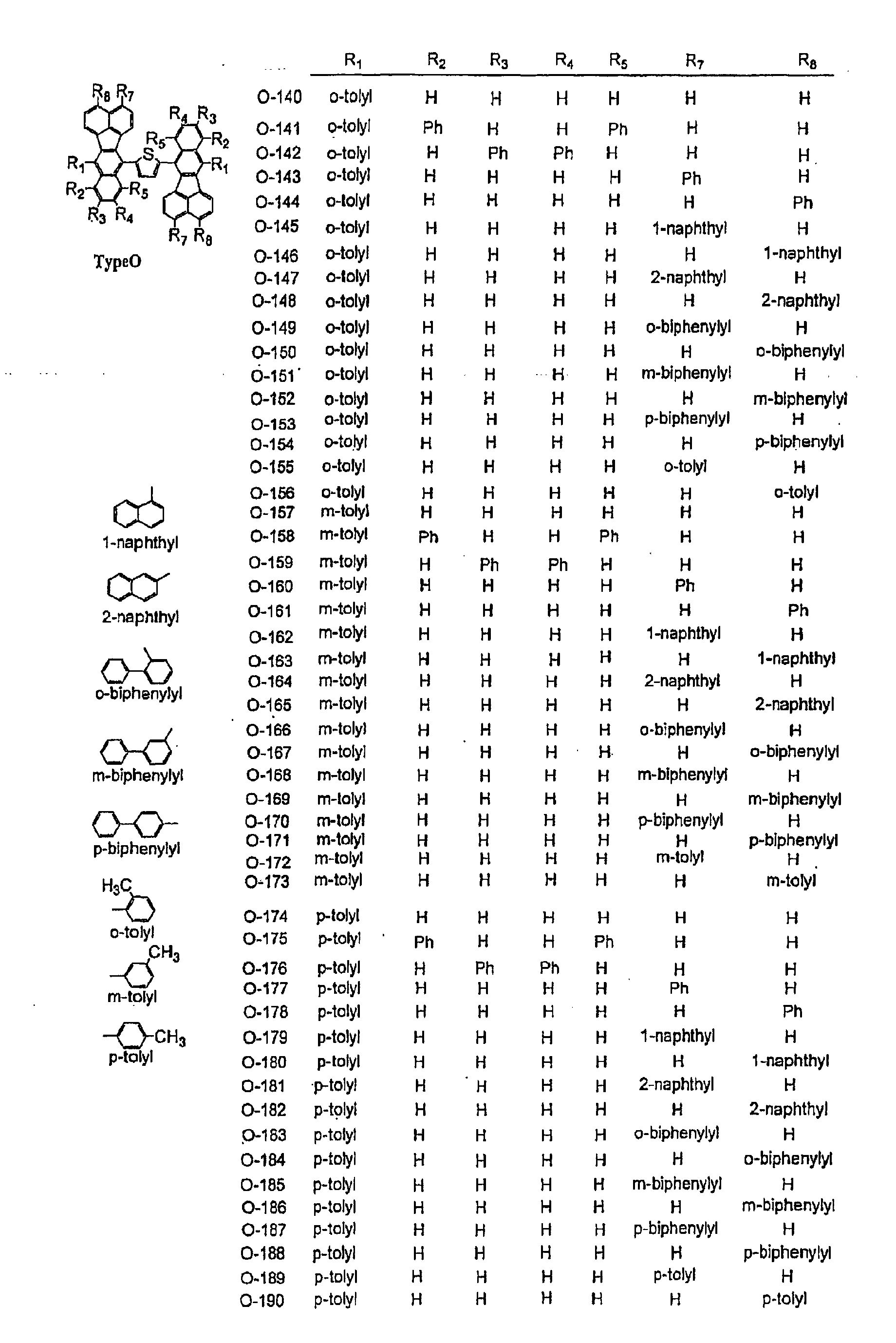















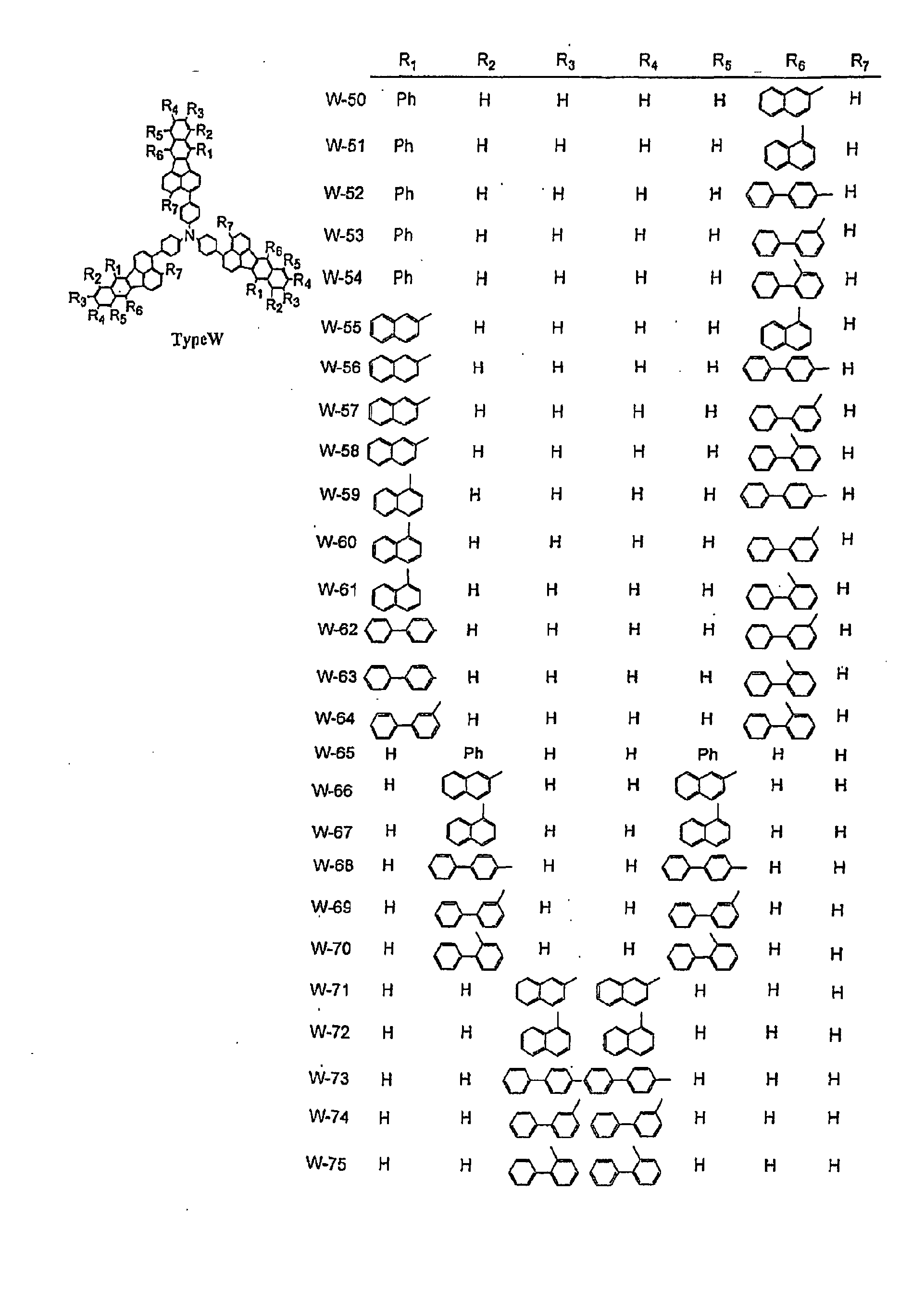
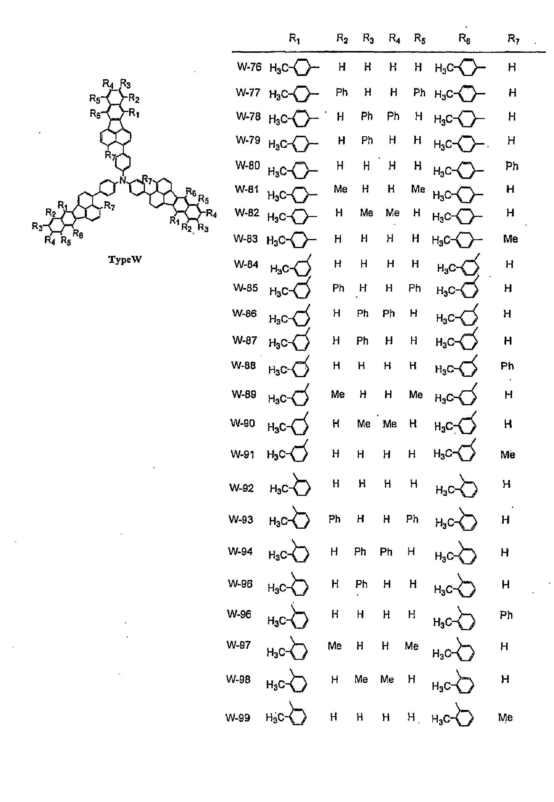
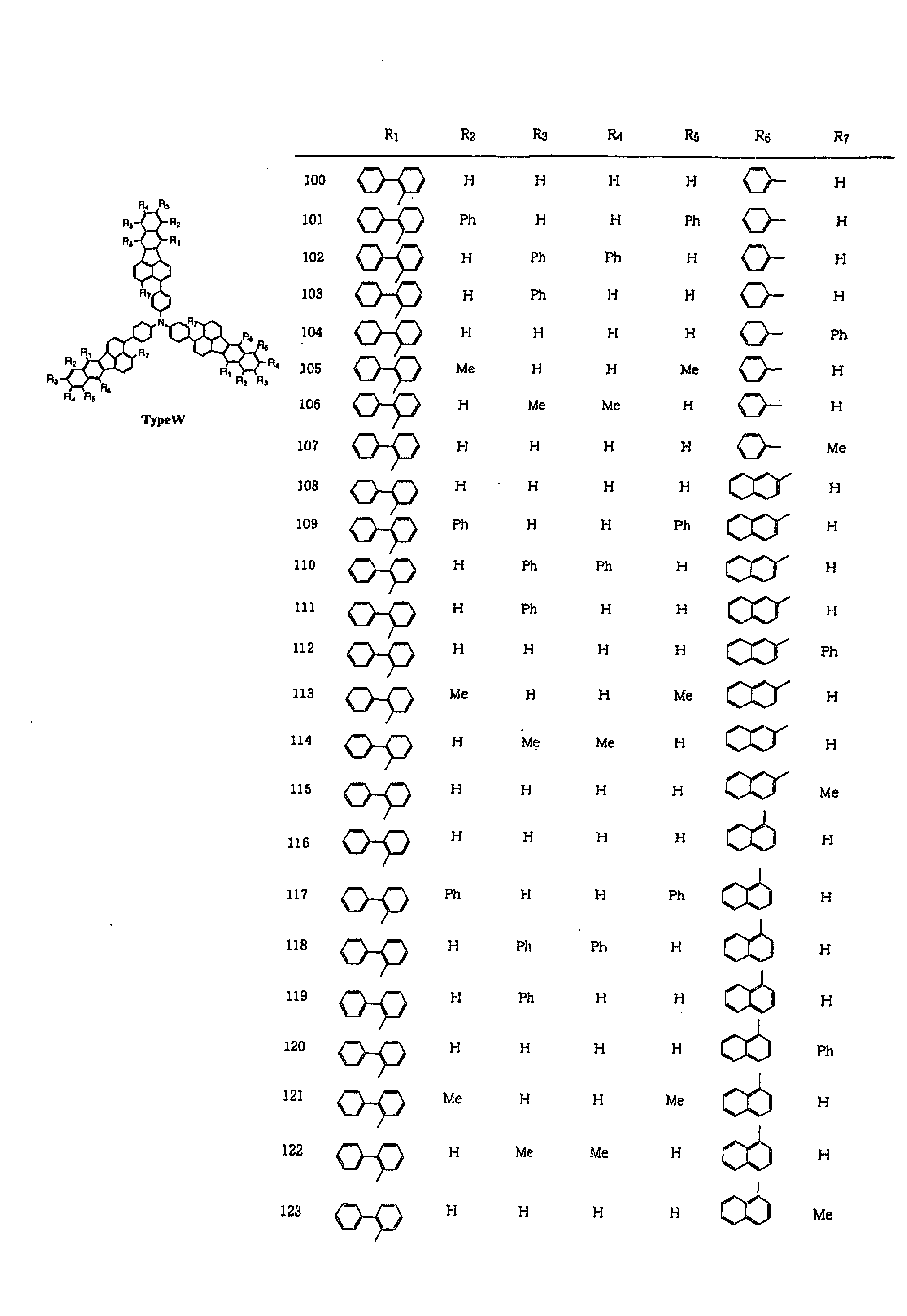


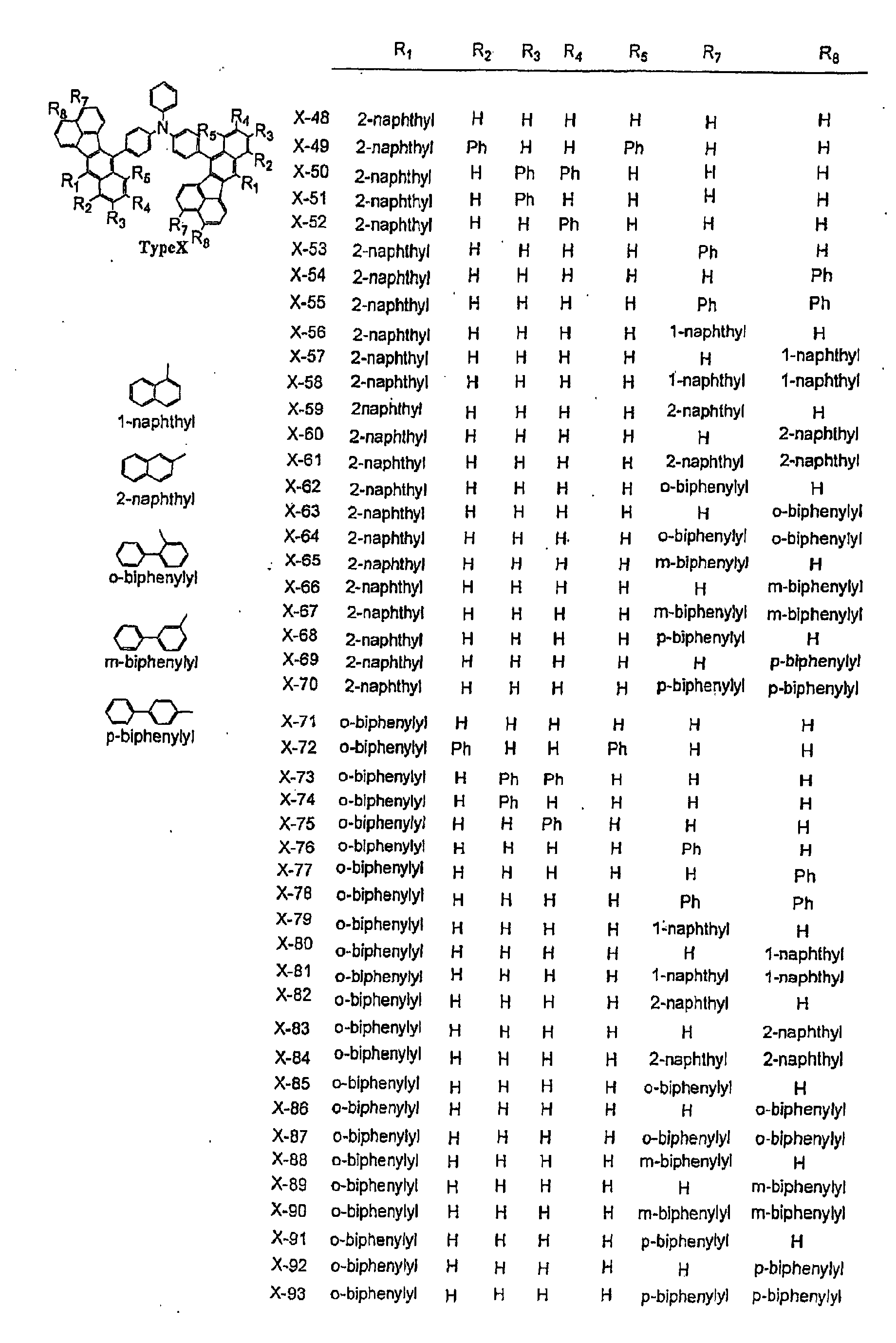







































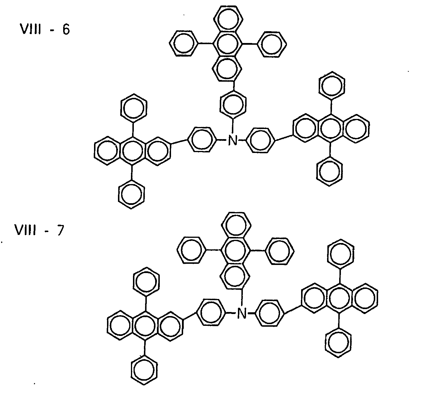


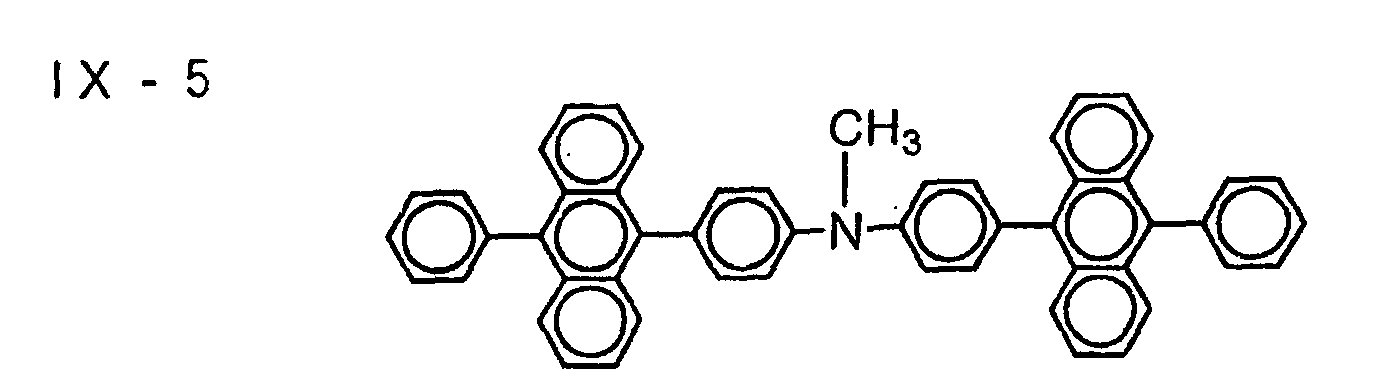
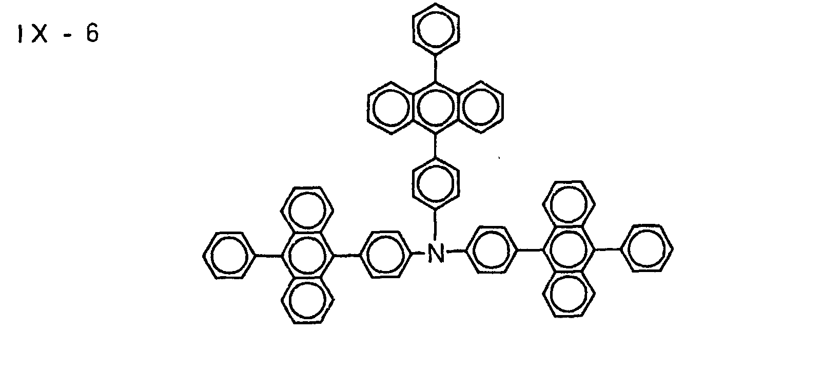

Exemplary are tetraarylbenzidine compounds (triaryldiamines or triphenyldiamines: TPD), aromatic tertiary amines, hydrazone derivatives, carbazole derivatives, triazole derivatives, imidazole derivatives, oxadiazole derivatives having an amino group, and polythiophenes. Two or more of these compounds may be used, and on such combined use, they may be formed as separate layers or mixed.
Mass spectrum m/e = 883 (M+1)+ FIG. 2
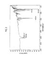
IR absorption spectrum FIG. 3
NMR FIG. 4
Glass transition temperature (Tg) 251°C
Mass spectrum m/e = 1050 (M+1)+
Mass spectrum m/e = 898 (M+1)+


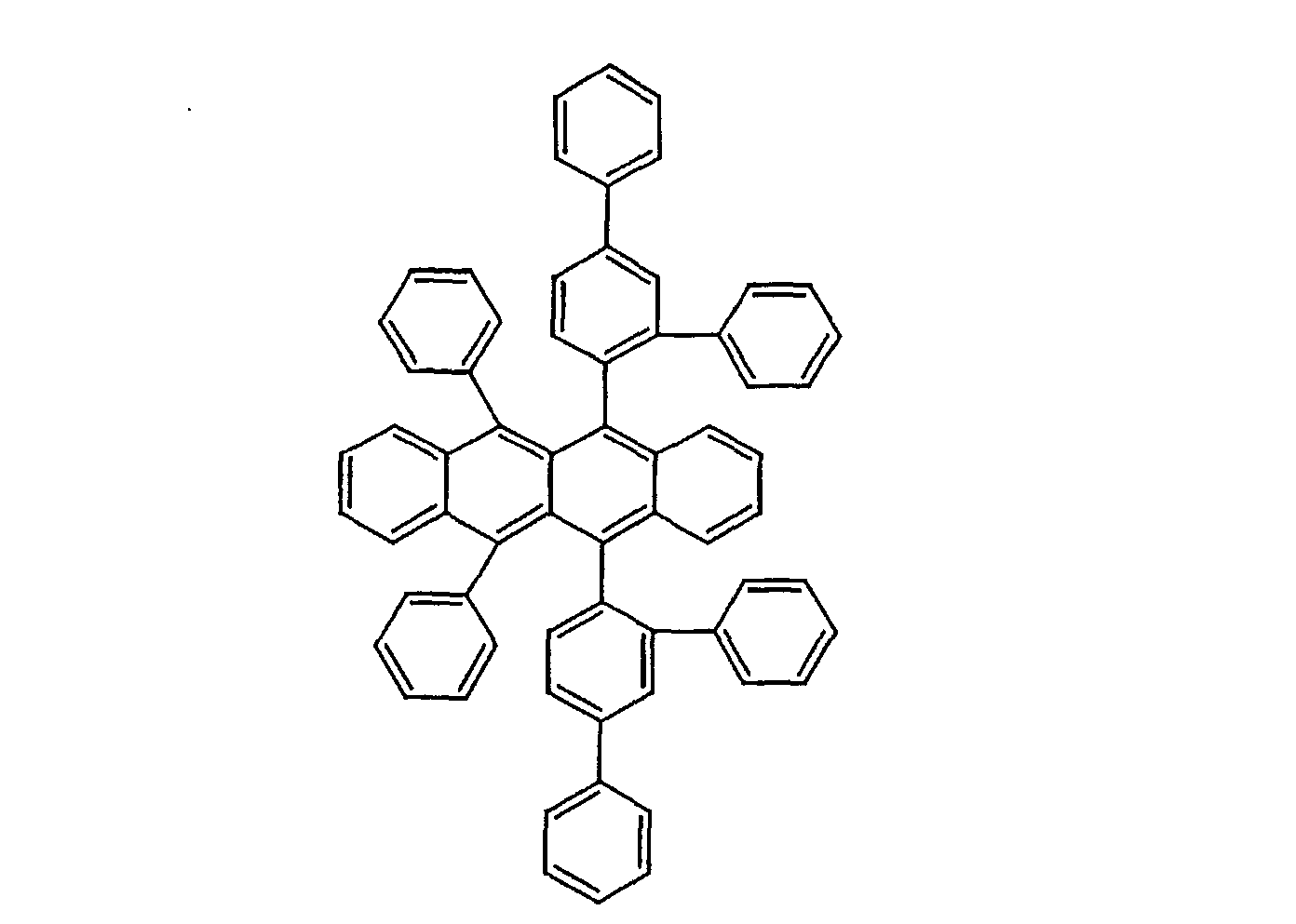




Claims (30)
- A compound for use in organic EL devices having a basic skeleton of the following formula (1):wherein R1 to R8 and a to d each are selected from among hydrogen, an alkyl group, an aryl group which may be substituted, an allyl group which may be substituted, a heterocyclic group which may be substituted, an amino group, and an arylamino group which may be substituted.
- The compound for use in organic EL devices of claim 1 wherein Y is at least one group selected from the following compounds:

- The compound for use in organic EL devices of claim 1 wherein n is 2.
- The compound for use in organic EL devices of claim 1 which is used as a dopant.
- The compound for use in organic EL devices of claim 1 which is an electron transporting material.
- The compound for use in organic EL devices of claim 1 which is a hole injecting or transporting material.
- The compound for use in organic EL devices of claim 1 having a basic skeleton of the following formula (3a):wherein R1 to R8, a1 to d1, R11 to R18 and a2 to d2 each are selected from among hydrogen, an alkyl group, an aryl group which may be substituted, an allyl group which may be substituted, a heterocyclic group which may be substituted, an amino group, and an arylamino group which may be substituted; Y is a linking group selected from the class consisting of substituted or unsubstituted phenylene, biphenylene, naphthacene, perylene, pyrene, phenanthrene, thiophene, pyridine, pyrazine, triazine, amine, triarylamine, pyrrole derivatives, thiazole, thiadiazole, phenanthroline, quinoline and quinoxaline.

- The compound for use in organic EL devices of claim 1 having a basic skeleton of the following formula (3b):wherein R1 to R8, a1 to d1, R11 to R18 and a2 to d2 each are selected from among hydrogen, an alkyl group, an aryl group which may be substituted, an allyl group which may be substituted, a heterocyclic group which may be substituted, an amino group, and an arylamino group which may be substituted; Y is a linking group selected from among a single bond, a substituted or unsubstituted aryl group, and a heterocyclic group.
- The compound for use in organic EL devices of claim 1 having a basic skeleton of the following formula (3c):wherein R1 to R8, a1 to d1, R11 to R18 and a2 to d2 each are selected from among hydrogen, an alkyl group, an aryl group which may be substituted, an allyl group which may be substituted, a heterocyclic group which may be substituted, an amino group, and an arylamino group which may be substituted; Y is a linking group selected from among a single bond, a substituted or unsubstituted aryl group, and a heterocyclic group.
- The compound for use in organic EL devices of claim 1 having a basic skeleton of the following formula (A):wherein R1 to R7 and R11 to R17 each are hydrogen, an alkyl group, a substituted or unsubstituted aryl group, or a heterocyclic group.
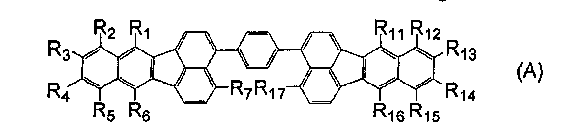
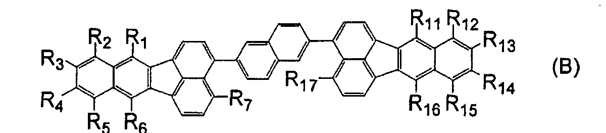
- The compound for use in organic EL devices of claim 1 having a basic skeleton of the following formula (B):wherein R1 to R7 and R11 to R17 each are hydrogen, an alkyl group, a substituted or unsubstituted aryl group, or a heterocyclic group.

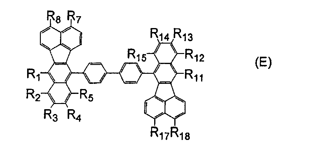
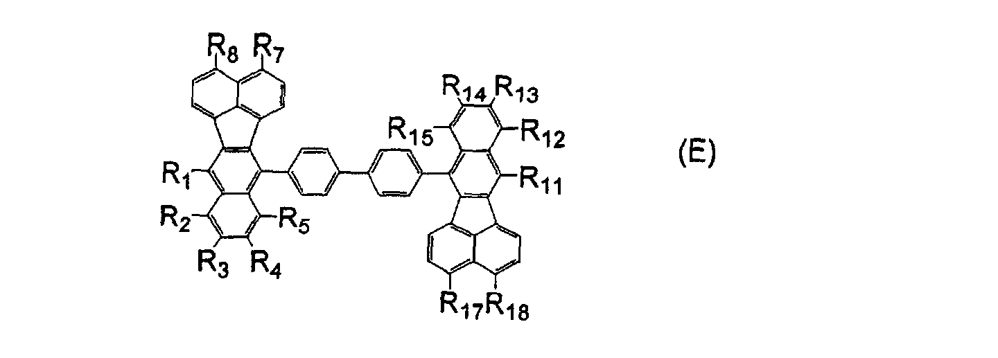
- The compound for use in organic EL devices of claim 1 having a basic skeleton of the following formula (E):wherein R1 to R8 and R11 to R18 each are hydrogen, an alkyl group, a substituted or unsubstituted aryl group, or a heterocyclic group.

- The compound for use in organic EL devices of claim 1 having a basic skeleton of the following formula (H):wherein R1 to R8 and R11 to R18 each are hydrogen, an alkyl group, a substituted or unsubstituted aryl group, or a heterocyclic group.

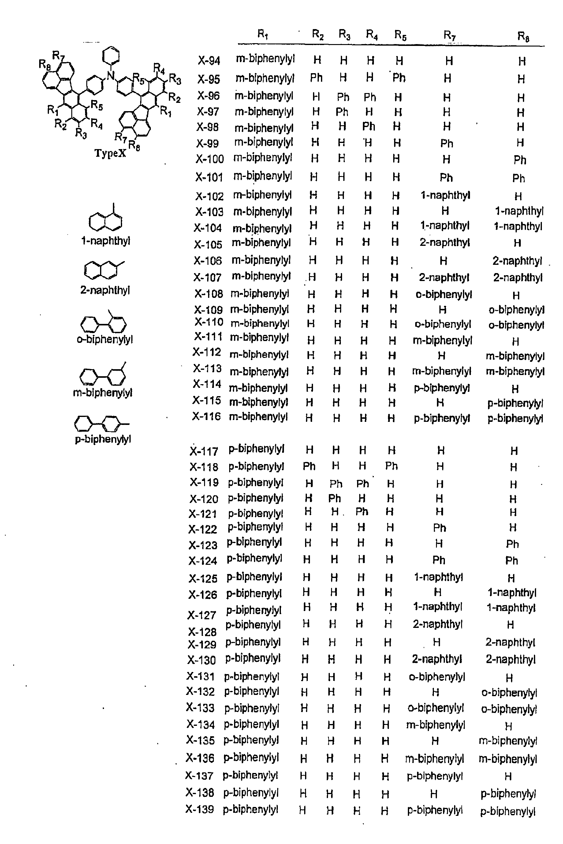
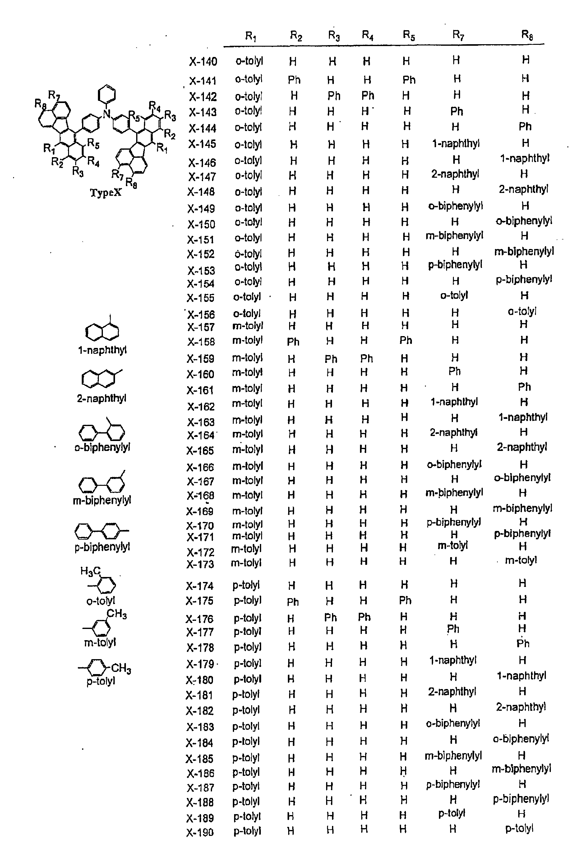
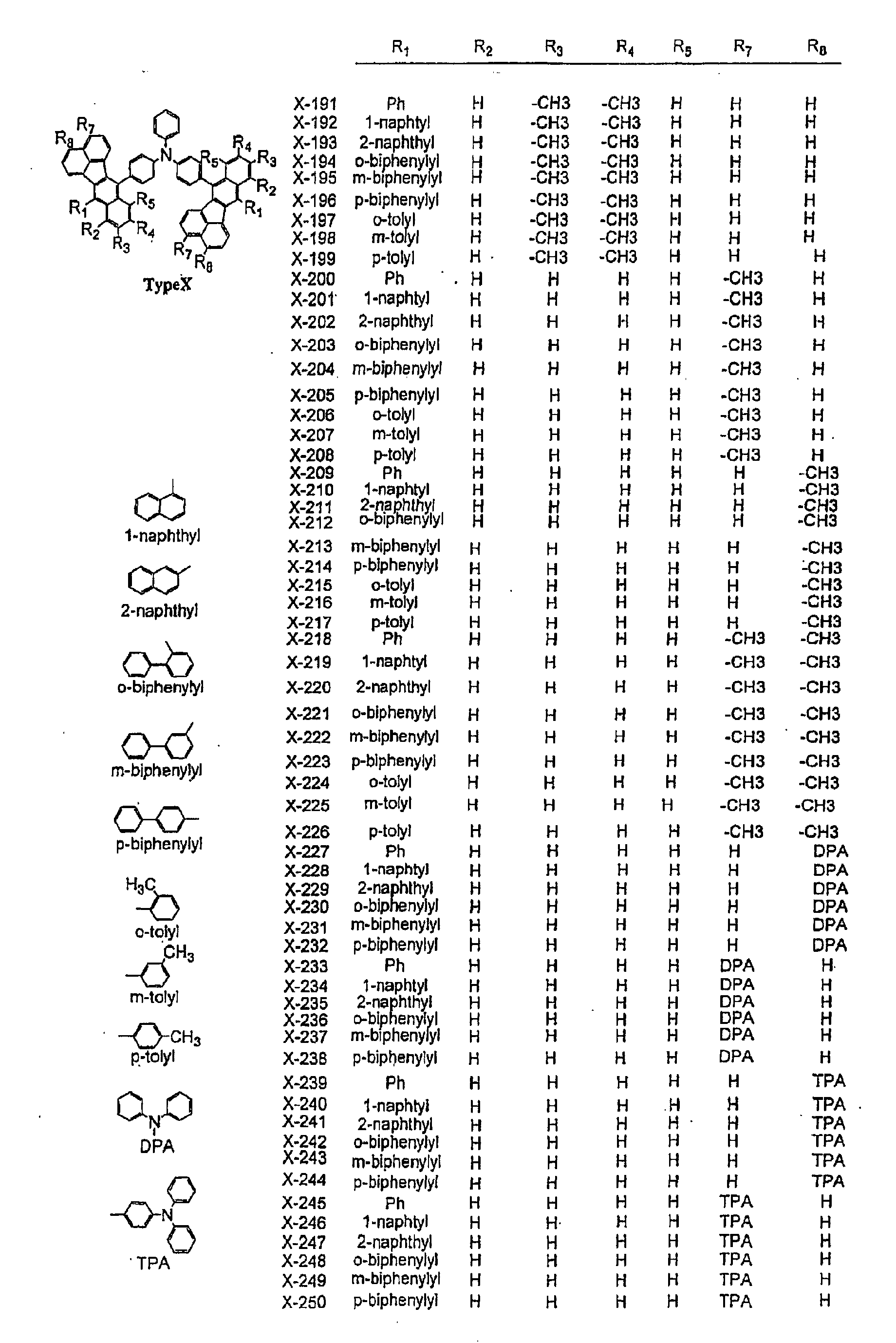
- The compound for use in organic EL devices of claim 1 having a basic skeleton of the following formula (X):wherein R1 to R8 and R11 to R18 each are hydrogen, an alkyl group, a substituted or unsubstituted aryl group, or a heterocyclic group.

- The compound for use in organic EL devices of claim 1 having a basic skeleton of the following formula (Z):wherein R1 to R7 and R11 to R17, R each are hydrogen, an alkyl group, a substituted or unsubstituted aryl group, or a heterocyclic group.
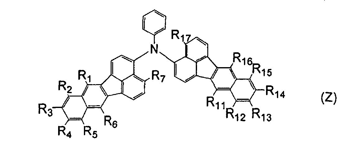
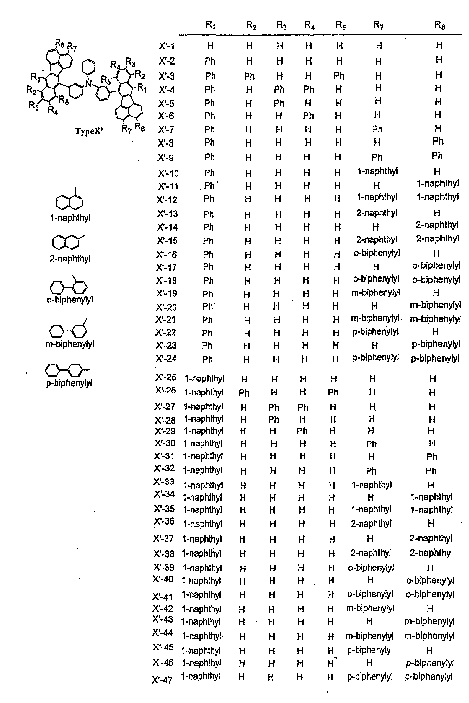
- The compound for use in organic EL devices of claim 1 having a basic skeleton of the following formula (AAA'):wherein R1 to R8 and R11 to R18 each are selected from among hydrogen, an alkyl group, an aryl group which may be substituted, an allyl group which may be substituted, a heterocyclic group which may be substituted, an amino group, and an arylamino group which may be substituted.

- The compound for use in organic EL devices of claim 1 having a basic skeleton of the following formula (BBB'):wherein R1 to R8 and R11 to R18 each are selected from among hydrogen, an alkyl group, an aryl group which may be substituted, an allyl group which may be substituted, a heterocyclic group which may be substituted, an amino group, and an arylamino group which may be substituted.

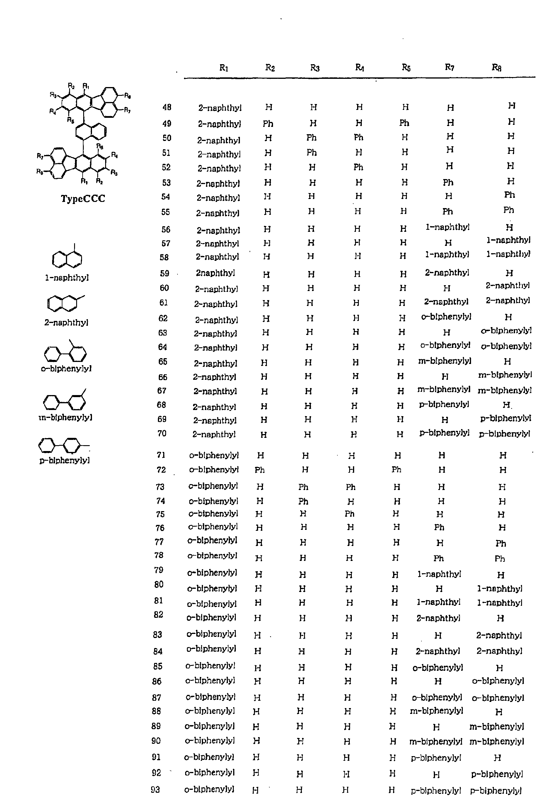
- The compound for use in organic EL devices of claim 1 having a basic skeleton of the following formula (CCC'):wherein R1 to R8 and R11 to R18 each are selected from among hydrogen, an alkyl group, an aryl group which may be substituted, an allyl group which may be substituted, a heterocyclic group which may be substituted, an amino group, and an arylamino group which may be substituted.

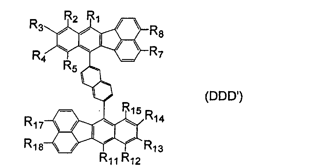
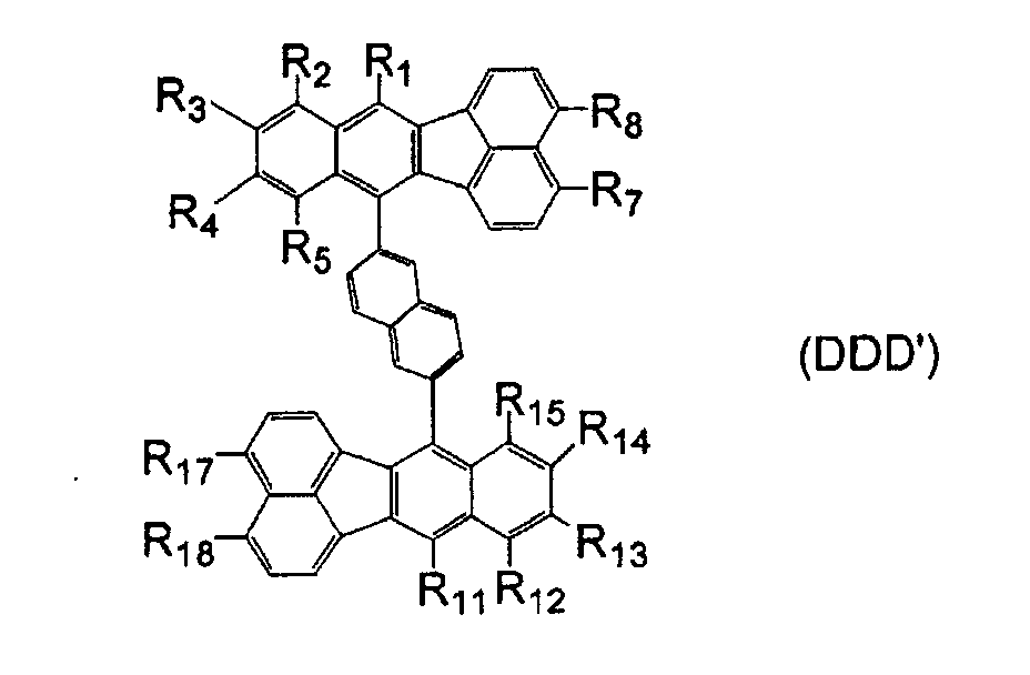
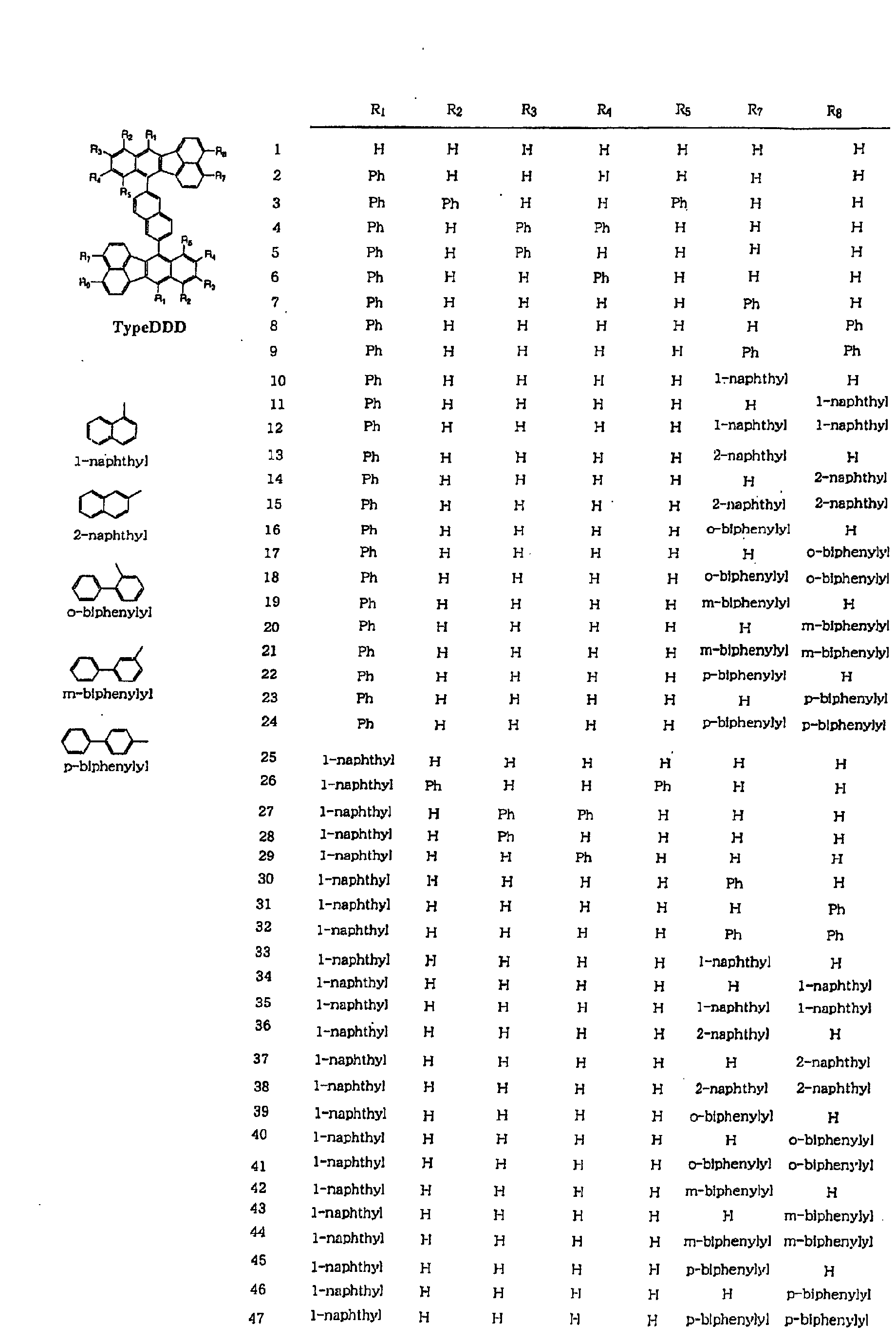
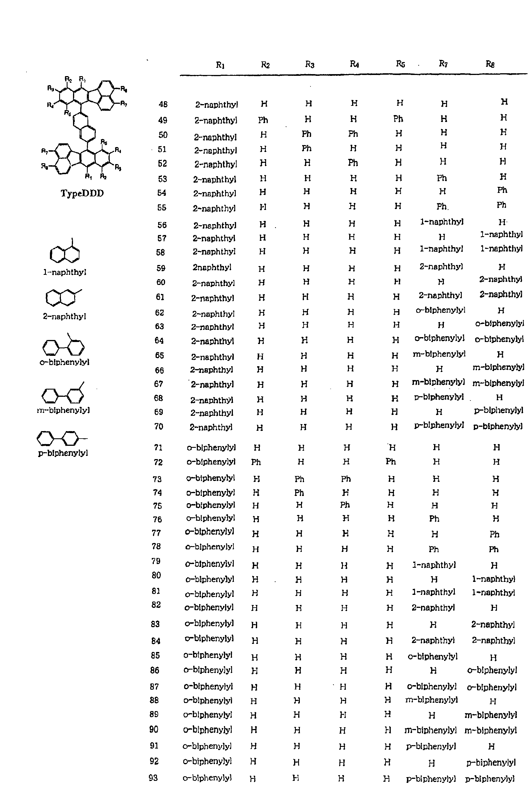
- The compound for use in organic EL devices of claim 1 having a basic skeleton of the following formula (DDD'):wherein R1 to R8 and R11 to R18 each are selected from among hydrogen, an alkyl group, an aryl group which may be substituted, an allyl group which may be substituted, a heterocyclic group which may be substituted, an amino group, and an arylamino group which may be substituted.

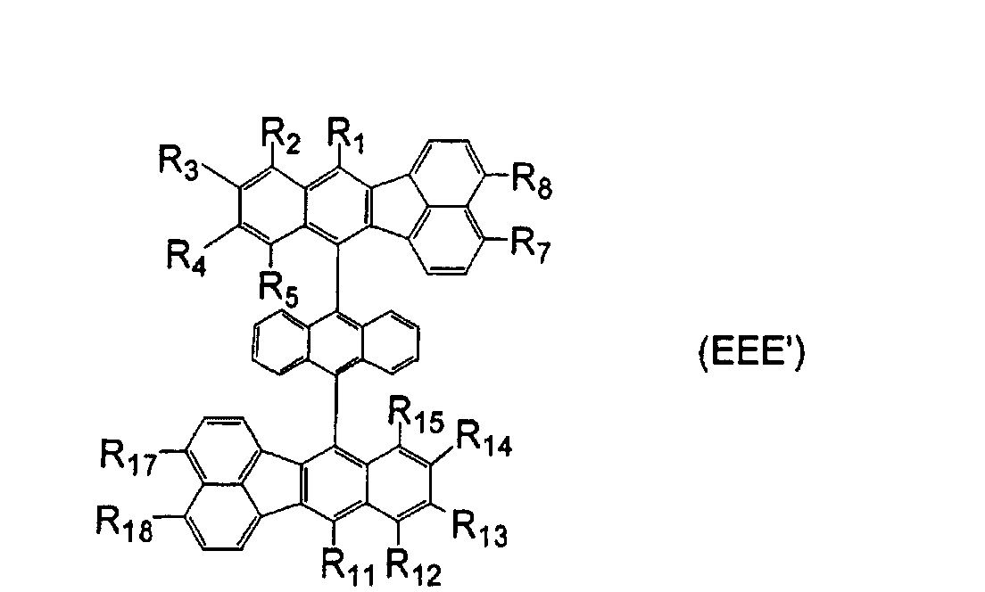
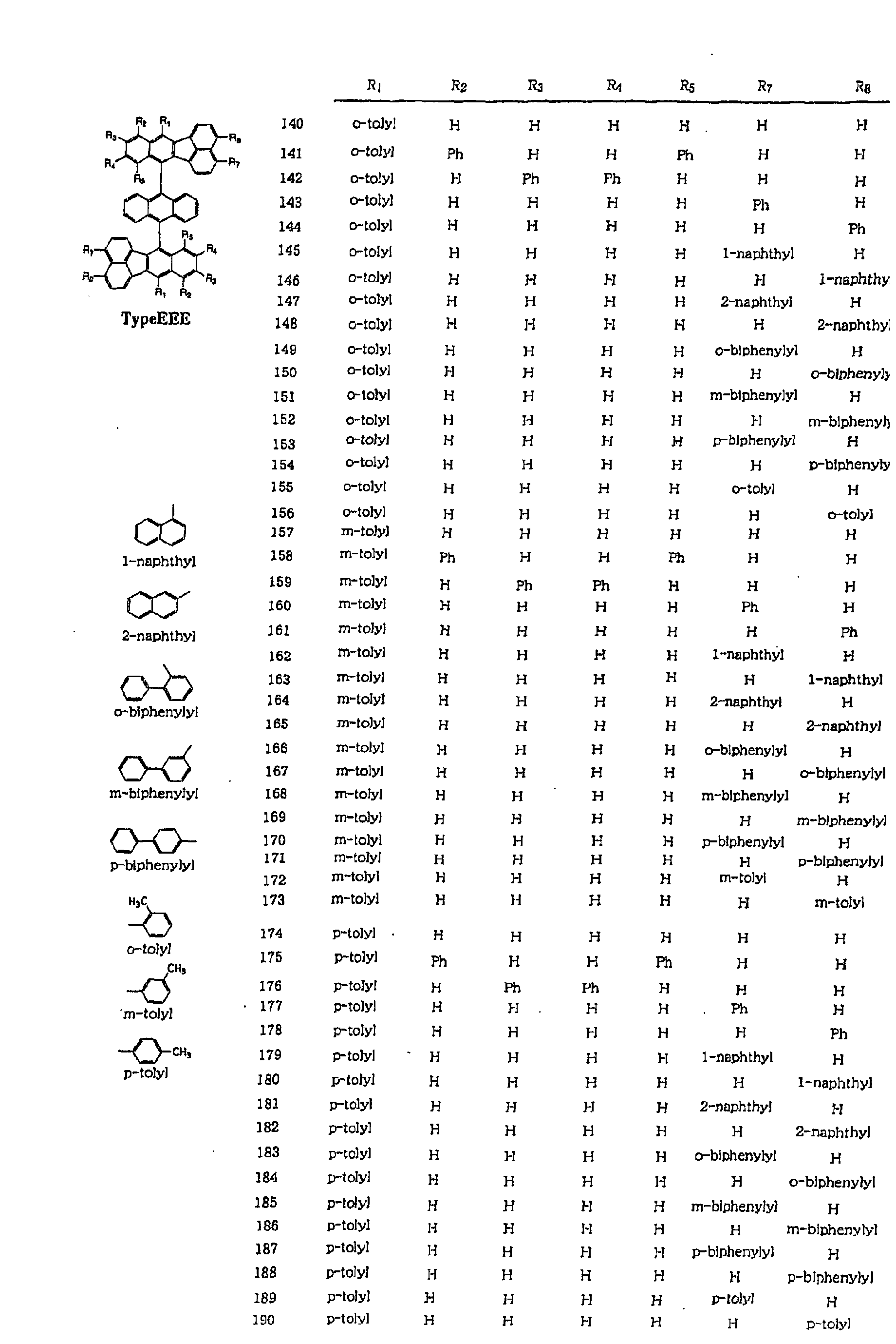
- The compound for use in organic EL devices of claim 1 having a basic skeleton of the following formula (EEE'):wherein R1 to R8 and R11 to R18 each are selected from among hydrogen, an alkyl group, an aryl group which may be substituted, an allyl group which may be substituted, a heterocyclic group which may be substituted, an amino group, and an arylamino group which may be substituted.
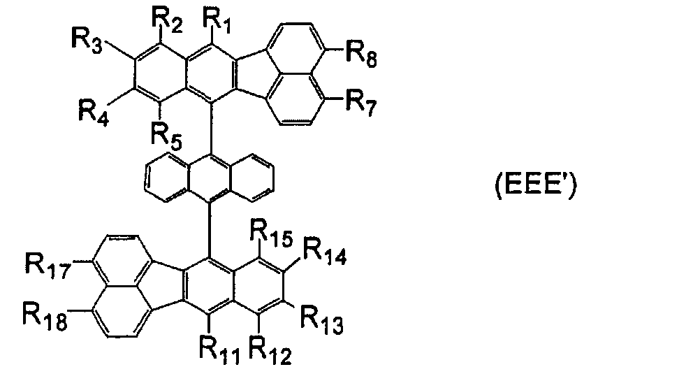
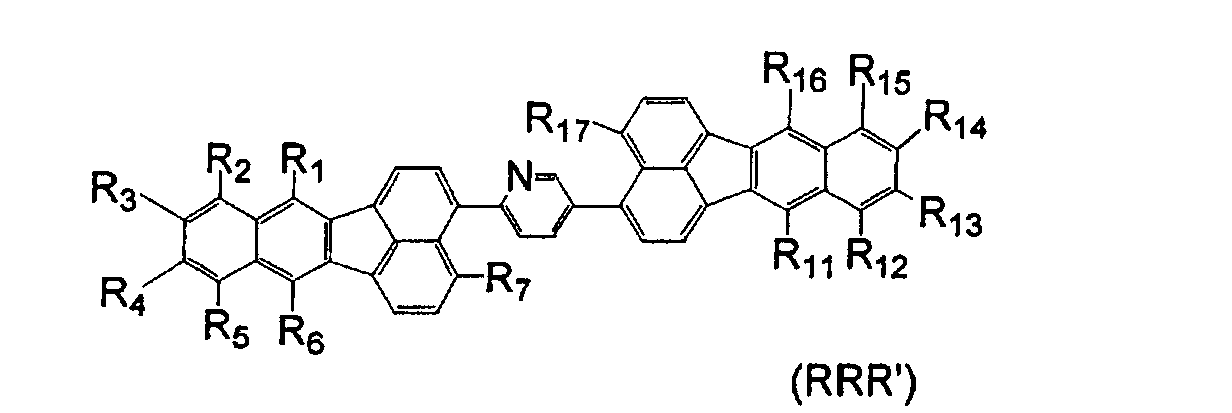
- The compound for use in organic EL devices of claim 1 having a basic skeleton of the following formula (RRR'):wherein R1 to R8 and R11 to R18 each are selected from among hydrogen, an alkyl group, an aryl group which may be substituted, an allyl group which may be substituted, a heterocyclic group which may be substituted, an amino group, and an arylamino group which may be substituted.
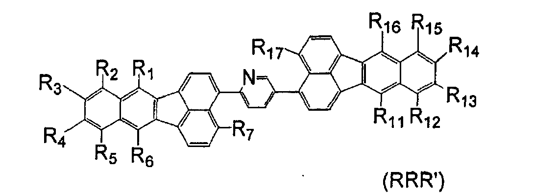
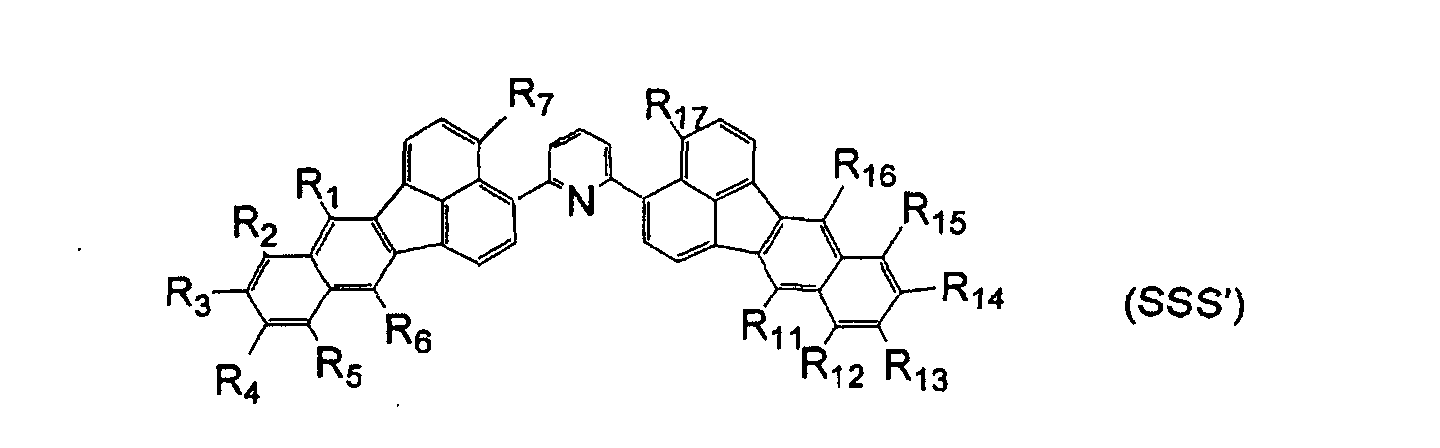
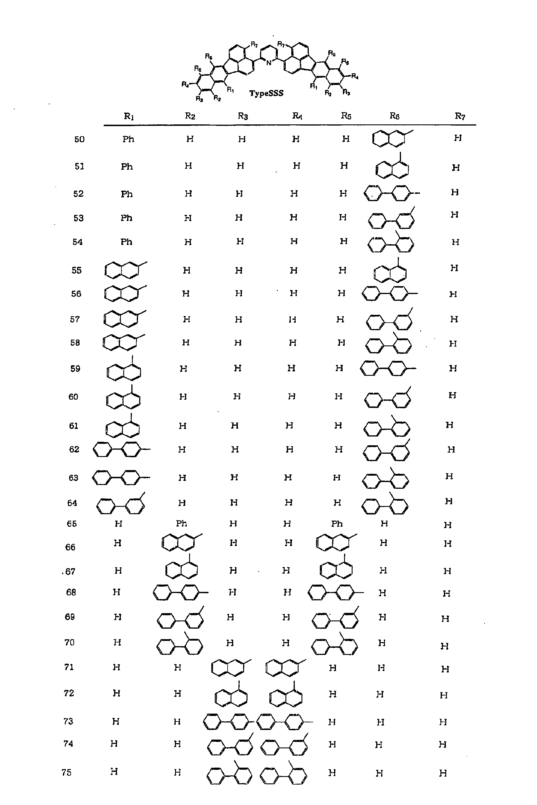
- The compound for use in organic EL devices of claim 1 having a basic skeleton of the following formula (SSS'):wherein R1 to R8 and R11 to R18 each are selected from among hydrogen, an alkyl group, an aryl group which may be substituted, an allyl group which may be substituted, a heterocyclic group which may be substituted, an amino group, and an arylamino group which may be substituted.

- An organic EL device comprising one or more organic layers between a pair of electrodes participating in at least a light emitting function,
at least one of the organic layers containing one or more compound for use in organic EL devices according to claim 1. - The organic EL device of claim 23, further comprising one or more anthracene compound in addition to the compound for use in organic EL devices.
- The organic EL device of claim 24 wherein the anthracene compound is contained as a host material for a light emitting layer.
- The organic EL device of claim 23 wherein the compound for use in organic EL devices is contained as a dopant.
- The organic EL device of claim 23 wherein the compound for use in organic EL devices is contained in a light emitting layer.
- The organic EL device of claim 23 wherein the compound for use in organic EL devices is contained in an electron transporting layer.
- The organic EL device of claim 23 wherein the compound for use in organic EL devices is contained in a hole injecting and transporting layer.
- The organic EL device of claim 23 exhibiting at least two maximum wavelengths of light emission ascribable to at least two light-emitting materials.
Priority Applications (1)
| Application Number | Priority Date | Filing Date | Title |
|---|---|---|---|
| EP06116129A EP1719748B1 (en) | 2001-04-19 | 2002-04-19 | Fluoranthene derivatives for use in organic electroluminescent devices |
Applications Claiming Priority (3)
| Application Number | Priority Date | Filing Date | Title |
|---|---|---|---|
| JP2001121788 | 2001-04-19 | ||
| JP2001121788 | 2001-04-19 | ||
| PCT/JP2002/003925 WO2002085822A1 (en) | 2001-04-19 | 2002-04-19 | Compound for organic el element and organic el element |
Related Child Applications (2)
| Application Number | Title | Priority Date | Filing Date |
|---|---|---|---|
| EP06116129A Division EP1719748B1 (en) | 2001-04-19 | 2002-04-19 | Fluoranthene derivatives for use in organic electroluminescent devices |
| EP06116129.5 Division-Into | 2006-06-27 |
Publications (3)
| Publication Number | Publication Date |
|---|---|
| EP1380556A1 true EP1380556A1 (en) | 2004-01-14 |
| EP1380556A4 EP1380556A4 (en) | 2004-08-25 |
| EP1380556B1 EP1380556B1 (en) | 2010-06-30 |
Family
ID=18971590
Family Applications (2)
| Application Number | Title | Priority Date | Filing Date |
|---|---|---|---|
| EP06116129A Expired - Lifetime EP1719748B1 (en) | 2001-04-19 | 2002-04-19 | Fluoranthene derivatives for use in organic electroluminescent devices |
| EP02722710A Expired - Lifetime EP1380556B1 (en) | 2001-04-19 | 2002-04-19 | Compound for organic el element and organic el element |
Family Applications Before (1)
| Application Number | Title | Priority Date | Filing Date |
|---|---|---|---|
| EP06116129A Expired - Lifetime EP1719748B1 (en) | 2001-04-19 | 2002-04-19 | Fluoranthene derivatives for use in organic electroluminescent devices |
Country Status (7)
| Country | Link |
|---|---|
| US (1) | US7097917B1 (en) |
| EP (2) | EP1719748B1 (en) |
| KR (1) | KR100554358B1 (en) |
| CN (1) | CN1325449C (en) |
| DE (2) | DE60236859D1 (en) |
| TW (1) | TW581751B (en) |
| WO (1) | WO2002085822A1 (en) |
Cited By (3)
| Publication number | Priority date | Publication date | Assignee | Title |
|---|---|---|---|---|
| EP2004580A4 (en) * | 2006-03-31 | 2009-07-15 | Canon Kk | INNOVATIVE COMPOUND AND ORGANIC ELECTROLUMINESCENT DEVICE USING THE COMPOUND |
| WO2010151654A1 (en) * | 2009-06-24 | 2010-12-29 | Cyalume Technologies, Inc. | Blue/violet diphenylanthracene chemiluminescent fluorescers |
| EP2190044A3 (en) * | 2008-11-19 | 2012-02-29 | Canon Kabushiki Kaisha | Light-emitting device, image display apparatus, and novel organic compound |
Families Citing this family (29)
| Publication number | Priority date | Publication date | Assignee | Title |
|---|---|---|---|---|
| US20040126617A1 (en) * | 2002-12-31 | 2004-07-01 | Eastman Kodak Company | Efficient electroluminescent device |
| JP2005123164A (en) * | 2003-09-24 | 2005-05-12 | Fuji Photo Film Co Ltd | Light emitting element |
| KR100721571B1 (en) * | 2005-03-07 | 2007-05-23 | 삼성에스디아이 주식회사 | Organic electroluminescent device and manufacturing method thereof |
| US9214636B2 (en) * | 2006-02-28 | 2015-12-15 | Idemitsu Kosan Co., Ltd. | Organic electroluminescence device |
| JP4819655B2 (en) * | 2006-04-27 | 2011-11-24 | キヤノン株式会社 | 4-Arylfluorene compound and organic light-emitting device using the same |
| KR101084100B1 (en) * | 2006-06-01 | 2011-11-16 | 가부시키가이샤 한도오따이 에네루기 켄큐쇼 | Light emitting element |
| JP5084208B2 (en) * | 2006-09-15 | 2012-11-28 | 出光興産株式会社 | ORGANIC ELECTROLUMINESCENT ELEMENT AND MATERIAL FOR ORGANIC ELECTROLUMINESCENT ELEMENT |
| US8277955B2 (en) * | 2006-10-17 | 2012-10-02 | Seiko Epson Corporation | Compound for organic EL device and organic EL device |
| EP2085371B1 (en) * | 2006-11-15 | 2015-10-07 | Idemitsu Kosan Co., Ltd. | Fluoranthene compound, organic electroluminescent device using the fluoranthene compound, and organic electroluminescent material-containing solution |
| US9397308B2 (en) * | 2006-12-04 | 2016-07-19 | Semiconductor Energy Laboratory Co., Ltd. | Light emitting element, light emitting device, and electronic device |
| JP5064787B2 (en) * | 2006-12-26 | 2012-10-31 | キヤノン株式会社 | Benzofluoranthene compound and organic light-emitting device using the same |
| US8779655B2 (en) * | 2007-07-07 | 2014-07-15 | Idemitsu Kosan Co., Ltd. | Organic electroluminescence device and material for organic electroluminescence device |
| US8129039B2 (en) | 2007-10-26 | 2012-03-06 | Global Oled Technology, Llc | Phosphorescent OLED device with certain fluoranthene host |
| US8431242B2 (en) | 2007-10-26 | 2013-04-30 | Global Oled Technology, Llc. | OLED device with certain fluoranthene host |
| US8420229B2 (en) | 2007-10-26 | 2013-04-16 | Global OLED Technologies LLC | OLED device with certain fluoranthene light-emitting dopants |
| US8076009B2 (en) | 2007-10-26 | 2011-12-13 | Global Oled Technology, Llc. | OLED device with fluoranthene electron transport materials |
| US7931975B2 (en) | 2008-11-07 | 2011-04-26 | Global Oled Technology Llc | Electroluminescent device containing a flouranthene compound |
| US8088500B2 (en) | 2008-11-12 | 2012-01-03 | Global Oled Technology Llc | OLED device with fluoranthene electron injection materials |
| JP2010121035A (en) * | 2008-11-19 | 2010-06-03 | Canon Inc | New organic compound, light-emitting element and imaging display |
| US7968215B2 (en) | 2008-12-09 | 2011-06-28 | Global Oled Technology Llc | OLED device with cyclobutene electron injection materials |
| JP5575547B2 (en) | 2010-05-28 | 2014-08-20 | 双葉電子工業株式会社 | Organic EL device |
| CN102731533B (en) | 2011-04-12 | 2016-08-10 | 精工爱普生株式会社 | Thiadiazole-based compound, compound for light-emitting device, light-emitting device, light-emitting device, authentication device, and electronic device |
| KR20130018547A (en) | 2011-08-09 | 2013-02-25 | 세이코 엡슨 가부시키가이샤 | Thiadiazole, light-emitting element, light-emitting apparatus, authentication apparatus, and electronic device |
| JP5970811B2 (en) | 2011-12-28 | 2016-08-17 | セイコーエプソン株式会社 | LIGHT EMITTING ELEMENT, LIGHT EMITTING DEVICE, AND ELECTRONIC DEVICE |
| US9324952B2 (en) | 2012-02-28 | 2016-04-26 | Seiko Epson Corporation | Thiadiazole, compound for light-emitting elements, light-emitting element, light-emitting apparatus, authentication apparatus, and electronic device |
| CN103772416B (en) | 2012-10-18 | 2018-01-19 | 精工爱普生株式会社 | Thiadiazole-based compound, compound for light-emitting device, light-emitting device, light-emitting device, authentication device, and electronic device |
| KR102167041B1 (en) * | 2013-08-14 | 2020-10-19 | 삼성디스플레이 주식회사 | Heterocyclic compound and organic light emitting device comprising same |
| CN111187225B (en) * | 2015-09-30 | 2021-06-11 | 北京鼎材科技有限公司 | Condensed ring aromatic hydrocarbon derivative with quinoxaline group and application thereof |
| CN108349932A (en) | 2015-10-27 | 2018-07-31 | 默克专利有限公司 | Materials for Organic Electroluminescent Devices |
Family Cites Families (18)
| Publication number | Priority date | Publication date | Assignee | Title |
|---|---|---|---|---|
| US4720432A (en) | 1987-02-11 | 1988-01-19 | Eastman Kodak Company | Electroluminescent device with organic luminescent medium |
| JP2651233B2 (en) | 1989-01-20 | 1997-09-10 | 出光興産株式会社 | Thin-film organic EL device |
| JPH03792A (en) | 1989-02-17 | 1991-01-07 | Pioneer Electron Corp | Electroluminescent element |
| US5061569A (en) | 1990-07-26 | 1991-10-29 | Eastman Kodak Company | Electroluminescent device with organic electroluminescent medium |
| JP3565870B2 (en) | 1992-02-25 | 2004-09-15 | 株式会社リコー | Electroluminescent device |
| JPH05299174A (en) | 1992-04-20 | 1993-11-12 | Ricoh Co Ltd | Organic thin film type el element |
| JP3274939B2 (en) | 1994-09-30 | 2002-04-15 | 松下電器産業株式会社 | EL device |
| JP3220950B2 (en) | 1993-11-01 | 2001-10-22 | 保土谷化学工業株式会社 | Benzidine compound |
| DE69412567T2 (en) | 1993-11-01 | 1999-02-04 | Hodogaya Chemical Co., Ltd., Tokio/Tokyo | Amine compound and electroluminescent device containing it |
| JP3574860B2 (en) | 1993-11-01 | 2004-10-06 | 保土谷化学工業株式会社 | Tetraphenylbenzidine compound |
| JP3794819B2 (en) | 1997-04-18 | 2006-07-12 | 三井化学株式会社 | Fluoranthene derivatives and organic electroluminescent devices |
| JPH11112205A (en) * | 1997-09-29 | 1999-04-23 | Kyocera Corp | Dielectric filter and filter device |
| JP3794846B2 (en) | 1998-12-17 | 2006-07-12 | 三井化学株式会社 | Hydrocarbon compounds and organic electroluminescent devices |
| JP3794847B2 (en) | 1998-12-21 | 2006-07-12 | 三井化学株式会社 | Hydrocarbon compounds and organic electroluminescent devices |
| JP3792096B2 (en) * | 2000-03-03 | 2006-06-28 | 三井化学株式会社 | Hydrocarbon compounds and organic electroluminescent devices |
| JP4274668B2 (en) * | 2000-03-10 | 2009-06-10 | 三井化学株式会社 | Hydrocarbon compounds and organic electroluminescent devices |
| JP4024009B2 (en) * | 2000-04-21 | 2007-12-19 | Tdk株式会社 | Organic EL device |
| JP4330055B2 (en) * | 2000-05-12 | 2009-09-09 | 三井化学株式会社 | Hydrocarbon compounds and organic electroluminescent devices |
-
2002
- 2002-04-19 DE DE60236859T patent/DE60236859D1/en not_active Expired - Lifetime
- 2002-04-19 DE DE60233080T patent/DE60233080D1/en not_active Expired - Lifetime
- 2002-04-19 CN CNB028013026A patent/CN1325449C/en not_active Expired - Fee Related
- 2002-04-19 TW TW091108294A patent/TW581751B/en not_active IP Right Cessation
- 2002-04-19 KR KR1020027017225A patent/KR100554358B1/en not_active Expired - Fee Related
- 2002-04-19 WO PCT/JP2002/003925 patent/WO2002085822A1/en not_active Ceased
- 2002-04-19 EP EP06116129A patent/EP1719748B1/en not_active Expired - Lifetime
- 2002-04-19 US US10/125,480 patent/US7097917B1/en not_active Expired - Lifetime
- 2002-04-19 EP EP02722710A patent/EP1380556B1/en not_active Expired - Lifetime
Cited By (7)
| Publication number | Priority date | Publication date | Assignee | Title |
|---|---|---|---|---|
| EP2004580A4 (en) * | 2006-03-31 | 2009-07-15 | Canon Kk | INNOVATIVE COMPOUND AND ORGANIC ELECTROLUMINESCENT DEVICE USING THE COMPOUND |
| US8072136B2 (en) | 2006-03-31 | 2011-12-06 | Canon Kabushiki Kaisha | Compound and organic light emitting device using the compound |
| US8384286B2 (en) | 2006-03-31 | 2013-02-26 | Canon Kabushiki Kaisha | Compound and organic light emitting device using the compound |
| CN101410356B (en) * | 2006-03-31 | 2013-08-07 | 佳能株式会社 | Novel compound and organic light-emitting device using the same |
| EP2190044A3 (en) * | 2008-11-19 | 2012-02-29 | Canon Kabushiki Kaisha | Light-emitting device, image display apparatus, and novel organic compound |
| WO2010151654A1 (en) * | 2009-06-24 | 2010-12-29 | Cyalume Technologies, Inc. | Blue/violet diphenylanthracene chemiluminescent fluorescers |
| US8257620B2 (en) | 2009-06-24 | 2012-09-04 | Cyalume Technologies, Inc. | Blue/violet diphenylanthracene chemiluminescent fluorescers |
Also Published As
| Publication number | Publication date |
|---|---|
| EP1719748A3 (en) | 2006-11-15 |
| CN1325449C (en) | 2007-07-11 |
| CN1464871A (en) | 2003-12-31 |
| KR100554358B1 (en) | 2006-02-24 |
| DE60236859D1 (en) | 2010-08-12 |
| EP1719748A2 (en) | 2006-11-08 |
| WO2002085822A1 (en) | 2002-10-31 |
| EP1380556B1 (en) | 2010-06-30 |
| DE60233080D1 (en) | 2009-09-03 |
| EP1719748B1 (en) | 2009-07-22 |
| TW581751B (en) | 2004-04-01 |
| EP1380556A4 (en) | 2004-08-25 |
| KR20030009541A (en) | 2003-01-29 |
| US7097917B1 (en) | 2006-08-29 |
Similar Documents
| Publication | Publication Date | Title |
|---|---|---|
| EP1719748B1 (en) | Fluoranthene derivatives for use in organic electroluminescent devices | |
| US6203933B1 (en) | Organic EL element | |
| JP4024009B2 (en) | Organic EL device | |
| US6150043A (en) | OLEDs containing thermally stable glassy organic hole transporting materials | |
| US6020078A (en) | Green organic electroluminescent devices | |
| JP3816969B2 (en) | Organic EL device | |
| KR100902524B1 (en) | Light emitting element and aromatic compound | |
| US6830829B2 (en) | Fused polynuclear compound and organic luminescence device | |
| KR100965811B1 (en) | 1,3,6,8-substituted pyrene compounds, organic EL devices and organic EL displays | |
| KR100701143B1 (en) | Organic electroluminescent element | |
| US5935720A (en) | Red organic electroluminescent devices | |
| EP0999256A1 (en) | Compounds for organic el element and organic el element | |
| JPWO1998030071A1 (en) | organic EL element | |
| JP4224252B2 (en) | Compound for organic EL element, organic EL element | |
| JP3650200B2 (en) | Organic EL devices using quinoxaline compounds | |
| JP2003040873A (en) | Novel quinoxaline derivative and organic electroluminescent device using the same | |
| KR101326668B1 (en) | Electron transporting-injection material and Organic electroluminescent device using the same | |
| JP2004002351A (en) | Organic EL device | |
| US7318965B2 (en) | Perylene derivative synthesis process, perylene derivative and organic EL device | |
| JP2003104916A (en) | Method for synthesizing perylene derivative, perylene derivative, and organic EL device | |
| KR20060121288A (en) | Stable Organic Light-Emitting Device Using Aminoanthracene | |
| JP2000016973A (en) | Novel triarylamine compound and light emitting device using the compound | |
| KR20040079803A (en) | organic electroluminescence device | |
| US20030113579A1 (en) | Dinaphthopyrene compound, and organic EL element and organic EL display using the same | |
| KR20090100438A (en) | Benzo [a] fluoranthene compound and organic light emitting device using the same |
Legal Events
| Date | Code | Title | Description |
|---|---|---|---|
| PUAI | Public reference made under article 153(3) epc to a published international application that has entered the european phase |
Free format text: ORIGINAL CODE: 0009012 |
|
| 17P | Request for examination filed |
Effective date: 20030802 |
|
| AK | Designated contracting states |
Kind code of ref document: A1 Designated state(s): AT BE CH CY DE DK ES FI FR GB GR IE IT LI LU MC NL PT SE TR |
|
| A4 | Supplementary search report drawn up and despatched |
Effective date: 20040714 |
|
| RIC1 | Information provided on ipc code assigned before grant |
Ipc: 7C 07C 13/62 A Ipc: 7C 07D 213/06 B Ipc: 7H 05B 33/22 B Ipc: 7C 07D 333/08 B Ipc: 7H 05B 33/14 B Ipc: 7C 07C 211/61 B Ipc: 7C 09K 11/06 B Ipc: 7C 07D 333/76 B Ipc: 7H 01L 51/30 B Ipc: 7C 07D 213/16 B Ipc: 7C 07C 211/54 B |
|
| GRAP | Despatch of communication of intention to grant a patent |
Free format text: ORIGINAL CODE: EPIDOSNIGR1 |
|
| GRAS | Grant fee paid |
Free format text: ORIGINAL CODE: EPIDOSNIGR3 |
|
| GRAA | (expected) grant |
Free format text: ORIGINAL CODE: 0009210 |
|
| AK | Designated contracting states |
Kind code of ref document: B1 Designated state(s): DE NL |
|
| REF | Corresponds to: |
Ref document number: 60236859 Country of ref document: DE Date of ref document: 20100812 Kind code of ref document: P |
|
| REG | Reference to a national code |
Ref country code: NL Ref legal event code: T3 |
|
| PLBE | No opposition filed within time limit |
Free format text: ORIGINAL CODE: 0009261 |
|
| STAA | Information on the status of an ep patent application or granted ep patent |
Free format text: STATUS: NO OPPOSITION FILED WITHIN TIME LIMIT |
|
| 26N | No opposition filed |
Effective date: 20110331 |
|
| REG | Reference to a national code |
Ref country code: DE Ref legal event code: R097 Ref document number: 60236859 Country of ref document: DE Effective date: 20110330 |
|
| REG | Reference to a national code |
Ref country code: DE Ref legal event code: R082 Ref document number: 60236859 Country of ref document: DE Representative=s name: VON KREISLER SELTING WERNER, DE |
|
| REG | Reference to a national code |
Ref country code: NL Ref legal event code: SD Effective date: 20120807 |
|
| REG | Reference to a national code |
Ref country code: DE Ref legal event code: R082 Ref document number: 60236859 Country of ref document: DE Representative=s name: VON KREISLER SELTING WERNER, DE Effective date: 20120814 Ref country code: DE Ref legal event code: R081 Ref document number: 60236859 Country of ref document: DE Owner name: FUTABA CORPORATION, JP Free format text: FORMER OWNER: TDK CORP., TOKYO, JP Effective date: 20120814 Ref country code: DE Ref legal event code: R082 Ref document number: 60236859 Country of ref document: DE Representative=s name: VON KREISLER SELTING WERNER - PARTNERSCHAFT VO, DE Effective date: 20120814 Ref country code: DE Ref legal event code: R081 Ref document number: 60236859 Country of ref document: DE Owner name: FUTABA CORPORATION, MOBARA-SHI, JP Free format text: FORMER OWNER: TDK CORP., TOKYO, JP Effective date: 20120814 Ref country code: DE Ref legal event code: R082 Ref document number: 60236859 Country of ref document: DE Representative=s name: DOMPATENT VON KREISLER SELTING WERNER - PARTNE, DE Effective date: 20120814 |
|
| PGFP | Annual fee paid to national office [announced via postgrant information from national office to epo] |
Ref country code: NL Payment date: 20180314 Year of fee payment: 17 |
|
| PGFP | Annual fee paid to national office [announced via postgrant information from national office to epo] |
Ref country code: DE Payment date: 20190410 Year of fee payment: 18 |
|
| REG | Reference to a national code |
Ref country code: NL Ref legal event code: MM Effective date: 20190501 |
|
| PG25 | Lapsed in a contracting state [announced via postgrant information from national office to epo] |
Ref country code: NL Free format text: LAPSE BECAUSE OF NON-PAYMENT OF DUE FEES Effective date: 20190501 |
|
| REG | Reference to a national code |
Ref country code: DE Ref legal event code: R119 Ref document number: 60236859 Country of ref document: DE |
|
| PG25 | Lapsed in a contracting state [announced via postgrant information from national office to epo] |
Ref country code: DE Free format text: LAPSE BECAUSE OF NON-PAYMENT OF DUE FEES Effective date: 20201103 |