EP1377084A2 - Kreuzschienenschalterstruktur mit eingangpositionsabhängiger Zwischenverstärkerstruktur - Google Patents
Kreuzschienenschalterstruktur mit eingangpositionsabhängiger Zwischenverstärkerstruktur Download PDFInfo
- Publication number
- EP1377084A2 EP1377084A2 EP03101772A EP03101772A EP1377084A2 EP 1377084 A2 EP1377084 A2 EP 1377084A2 EP 03101772 A EP03101772 A EP 03101772A EP 03101772 A EP03101772 A EP 03101772A EP 1377084 A2 EP1377084 A2 EP 1377084A2
- Authority
- EP
- European Patent Office
- Prior art keywords
- crossbar
- inputs
- specified
- repeater
- circuit
- Prior art date
- Legal status (The legal status is an assumption and is not a legal conclusion. Google has not performed a legal analysis and makes no representation as to the accuracy of the status listed.)
- Withdrawn
Links
Images


Classifications
-
- H—ELECTRICITY
- H04—ELECTRIC COMMUNICATION TECHNIQUE
- H04Q—SELECTING
- H04Q3/00—Selecting arrangements
- H04Q3/42—Circuit arrangements for indirect selecting controlled by common circuits, e.g. register controller, marker
- H04Q3/52—Circuit arrangements for indirect selecting controlled by common circuits, e.g. register controller, marker using static devices in switching stages, e.g. electronic switching arrangements
- H04Q3/521—Circuit arrangements for indirect selecting controlled by common circuits, e.g. register controller, marker using static devices in switching stages, e.g. electronic switching arrangements using semiconductors in the switching stages
-
- H—ELECTRICITY
- H04—ELECTRIC COMMUNICATION TECHNIQUE
- H04Q—SELECTING
- H04Q2213/00—Indexing scheme relating to selecting arrangements in general and for multiplex systems
- H04Q2213/13003—Constructional details of switching devices
-
- H—ELECTRICITY
- H04—ELECTRIC COMMUNICATION TECHNIQUE
- H04Q—SELECTING
- H04Q2213/00—Indexing scheme relating to selecting arrangements in general and for multiplex systems
- H04Q2213/1302—Relay switches
-
- H—ELECTRICITY
- H04—ELECTRIC COMMUNICATION TECHNIQUE
- H04Q—SELECTING
- H04Q2213/00—Indexing scheme relating to selecting arrangements in general and for multiplex systems
- H04Q2213/1304—Coordinate switches, crossbar, 4/2 with relays, coupling field
-
- H—ELECTRICITY
- H04—ELECTRIC COMMUNICATION TECHNIQUE
- H04Q—SELECTING
- H04Q2213/00—Indexing scheme relating to selecting arrangements in general and for multiplex systems
- H04Q2213/1305—Software aspects
-
- H—ELECTRICITY
- H04—ELECTRIC COMMUNICATION TECHNIQUE
- H04Q—SELECTING
- H04Q2213/00—Indexing scheme relating to selecting arrangements in general and for multiplex systems
- H04Q2213/13054—Expert system
-
- H—ELECTRICITY
- H04—ELECTRIC COMMUNICATION TECHNIQUE
- H04Q—SELECTING
- H04Q2213/00—Indexing scheme relating to selecting arrangements in general and for multiplex systems
- H04Q2213/13191—Repeater
-
- H—ELECTRICITY
- H04—ELECTRIC COMMUNICATION TECHNIQUE
- H04Q—SELECTING
- H04Q2213/00—Indexing scheme relating to selecting arrangements in general and for multiplex systems
- H04Q2213/13322—Integrated circuits
Definitions
- the present invention is generally related to crossbar circuits, and more particularly to large crossbar circuits utilized in large integrated circuits such as VLSI chips.
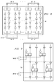
- Crossbars are structures which can connect any input to any output. It is common in VLSI chips to implement large crossbars, such as shown at 10 in Figure 1, to switch inputs coupled to one circuit block 12 to outputs feeding a second circuit block 14.
- a crossbar may have 64 inputs and 64 outputs, where each of the inputs and outputs is 16 bits wide.
- the crossbar is built largely out of multiplexers, where each output is driven by a 16 bit wide, 64 input multiplexer.
- the 64 input mux is in practice implemented as a tree of smaller muxes. With 64 crossbar outputs, there are 64 instances of this 64-input, 16 bit wide mux.
- Crossbars conventionally can be efficiently implemented as regular datapath structures, where each output mux is a bitstack, or a regular datapath component.
- the 64 output muxes are then placed in a sequence. For example, as shown at 16 in Figure 2, the mux bitstacks are horizontal, with bit 0 on the left and bit 15 on the right.
- the datapath is then built up vertically, with output mux 0 on the bottom and output mux 63 on the top.
- each of the 64 16 bit input wires must be broadcast to all 64 output muxes.
- Figure 3 shows these 1024 wires at 18 running vertically the entire height of the crossbar 10. It is typically the case that the load represented by the inputs of the 64 muxes is too large to be driven by a single wire, where the wire 18 is long enough that the resulting RC time constant is unacceptable.
- repeaters 20 must be inserted in the input wires 18, as shown in Figure 4 for the case of an input wire divided into 4 segments by 3 repeaters.
- the output data wires 18 may also be registered by registers 22, as shown in Figure 5, giving a full clock cycle for the crossbar to function, and allowing time for the input and output signals on the wires 18 to travel potentially long distances.
- the repeaters 20 are driven from the buffered output of the registers.
- Figure 5 The arrangement of Figure 5 is a conventional case where all 1024 data input wires are input to the bottom of the crossbar module. It is also possible to input wires to the top of the module, as shown in Figure 6, using repeaters to form a basic repeater structure as shown.
- the present invention achieves technical advantages as a crossbar circuit having a plurality of repeaters forming different repeater arrangements, whereby inputs to the crossbar circuit are defined about a perimeter of the circuit, with each input coupled to one repeater arrangement and being configured as a function of the input location relative to the crossbar circuit on the die.
- the repeater topology is dependent upon the physical location of the repeater structure in the crossbar, which location is a function of the input locations to be interconnected thereto.
- the muxes are petitioned into mux groups, wherein each mux group is driven by repeaters positioned proximate to the respective group.
- Each input preferably has the plurality of bits, wherein the repeater arrangement is provided for each bit.
- the various repeater arrangements comprise serially connected repeaters, and a data register associated with each repeater arrangement may feed the repeater arrangements at different sections thereof. For instance, one data register may feed the end of the repeater structure, while other data registers feed the midsection of the repeater arrangements, depending upon where the input to the respective data register is located relative to the die periphery.
- the data register/repeater arrangements are adapted to be programmed by a pseudo code and executed by a layout compiler, such that inputs are selectively coupled to the repeater arrangements as a function of the relative position of the input at the crossbar periphery.
- the inputs can be selectively arranged about the perimeter of the crossbar die such that the crossbar can be custom configured to interface to other circuit blocks designed thereabout for a particular design.
- the present invention derives technical advantages as a crossbar accommodating inputs from many sides to interconnect large circuits defined about the periphery of the crossbar.
- the arrangement of repeaters in the crossbar is different, as shown at 30 and 40 in Figures 7-8.
- Figure 8 shows a crossbar 40 having some inputs coming from the bottom and some from the top of the crossbar module.
- inputs 0-31 arrive, with the 32 vertically extending wires for bit 0 on the left, and then 32 wires for each successive bit until finally the 32 input wires for bit 15 lie on the right.
- bit 0 is on the left and bit 15 is on the right with downwardly extending wires.
- Each of these wires includes repeaters 42 forming a repeater topology as a function of the input location as will now be discussed further.
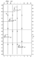
- Figure 9 shows a crossbar arrangement at 50 where some inputs are defined at the left side of the crossbar.
- the 16 bits of input 12 arrive in sequence, following which are the 16 input bits of the next input. Further up the left side of the crossbar, the 16 bits of input 27 are shown arriving in sequence.
- the relative location of the input relative to the crossbar determines the associated repeater structure topology, as shown.
- Nseg the number of segments the data input wires will be broken into is determined, identified as Nseg.
- Nseg repeater buffers 62 driving each wire, where one of the wire segments is driven directly by a buffer off the data input register 22, and the other segments are driven from other respective repeaters 62.
- the signal naming of the 4 repeated versions of a data input signal is as follows: dinbuf[inpsig][repeat] ⁇ bit> where "inpsig” ranges from 0 to 63 for the 64 data inputs, “repeat” ranges from 0 to 3 for the 4 segments of the buffered data input wire, and "bit” ranges from 0 to 15.
- the index repeat corresponds to the physical location of the data input wire segment, from 0 on the bottom to 3 on the top. Namely: The bottom 16 output muxes 0 to 15 are fed from the wires: dinbuf[inpsig][0] ⁇ bit>, the next adjacent 16 output muxes 16-31 are fed from the wires: dinbuf[inpsig] [1] ⁇ bit>, the next adjacent 16 output muxes 32-47 are fed from the wires: dinbuf[inpsig][2] ⁇ bit>, and the last adjacent 16 output muxes 48-63 are fed from the wires: dinbuf[inpsig][3] ⁇ bit>.
- Input_segment be a function which given the data input number, returns which segment the data input lies in. This function can be designed custom for each crossbar application to indicate desired port locations, allowing flexibility in design. In this example, inputs at the bottom of the crossbar return 0, inputs at the top of the crossbar return 3, and other inputs along the left or right sides of the crossbar return from 0 to 3, depending on which 25% of the crossbar height they fell upon.
- Each arrow in the line represents one repeater out of the final 3 repeaters in the sequence, located at the 25%, 50% and 75% portions along the vertical extent of the crossbar module. If the input is below repeater 1 at the 25% point, repeater 1 takes dinbuf[inpsig][0] and produces dinbuf[inpsig][1], i.e., 0->1. If the input is above repeater 1 at the 25% point, repeater 1 takes dinbuf[inpsig][1] and produces dinbuf[inpsig][0], i.e., 1->0.
- the first buffer driven from the registered data input, has a repeat index corresponding to its physical location, so for an input arriving in segment 2, the buffers would produce signals: dinbuf[data_input][2] ⁇ bit>.
- a crossbar 60 will be discussed which has 64 inputs and 64 outputs, each 16 bits wide.
- the 64 inputs are distributed to all 4 sides of the crossbar module periphery, with 16 inputs per side. Inputs 0-15 come from the bottom, inputs 16-31 come from the right side, inputs 32-47 come from the top and inputs 48-63 come from the left side.
- each of the vertical data input wires are separated into 4 segments, each separated from the next by a repeater 62.
- a function input_segment which for each data input, returns which input segment the data falls into.
- Inputs 0-15 on the bottom belong to segment 0, while inputs 32-47 on the top belong to segment 3.
- Inputs 16-31 on the right side are distributed among the four segments, with four consecutive inputs to each segment. Thus: inputs 16-19 belong to segment 0 inputs 20-23 belong to segment 1 inputs 24-27 belong to segment 2 inputs 28-31 belong to segment 3.
- Inputs 48-63 on the left are distributed among the four segments, with four consecutive inputs to each segment.
- inputs 48-51 belong to segment 3
- inputs 52-55 belong to segment 2
- inputs 56-59 belong to segment 1 inputs 60-63 belong to segment 0.
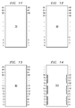
- a crossbar 70 is shown in Figure 11, again with 64 inputs and 64 outputs, each 16 bits wide.
- the data input wires are again separated into 4 segments. This time, the data inputs will all come from the left and right sides of the crossbar, alternating sides, starting from the bottom.
- Figure 12 shows a crossbar 80 with the inputs alternating from left to right in a serpentine pattern.
- Figure 13 shows a crossbar 90 with the inputs alternating from left to right in groups of 4 signals; first 4 on the left, then 4 on the right, etc.
- Figure 14 shows a crossbar 100 with the inputs serpentining from left to right, in groups of 4 signals; where they are on the left, then right, right, left sides. All of these data input pin location patterns in Figures 12-14 share the same input_segment function above.
- the algorithm for defining the crossbar configuration is as follows: Let there be N output muxes. Let there be Nseg segments in the data input wires, with repeaters between them, so that each wire drives N/Nseg output muxes. Divide the output muxes into Nseg groups of physically adjacent muxes, numbered from 0 to Nseg-1. Then, muxes in group K from 0 to Nseg-1 are driven by data input wire segment K. Let input_segment be which one of the Nseg groups a data input wire port physically lies in. Let the registered data input be called din q.
- the first buffer takes din_q as its input and produces dinbuf[input_segment] as its output.
- buffer M takes dinbuf[M] as its input and produces dinbuf[M-1] as its output.
- buffer M takes dinbuf[M-1] as its input and produces dinbuf[M] as its output.
Landscapes
- Engineering & Computer Science (AREA)
- Computer Networks & Wireless Communication (AREA)
- Logic Circuits (AREA)
- Semiconductor Integrated Circuits (AREA)
- Electronic Switches (AREA)
Applications Claiming Priority (2)
| Application Number | Priority Date | Filing Date | Title |
|---|---|---|---|
| US10/174,123 US6970967B2 (en) | 2002-06-18 | 2002-06-18 | Crossbar circuit having a plurality of repeaters forming different repeater arrangements |
| US174123 | 2002-06-18 |
Publications (2)
| Publication Number | Publication Date |
|---|---|
| EP1377084A2 true EP1377084A2 (de) | 2004-01-02 |
| EP1377084A3 EP1377084A3 (de) | 2005-11-30 |
Family
ID=29717792
Family Applications (1)
| Application Number | Title | Priority Date | Filing Date |
|---|---|---|---|
| EP03101772A Withdrawn EP1377084A3 (de) | 2002-06-18 | 2003-06-17 | Kreuzschienenschalterstruktur mit eingangpositionsabhängiger Zwischenverstärkerstruktur |
Country Status (3)
| Country | Link |
|---|---|
| US (1) | US6970967B2 (de) |
| EP (1) | EP1377084A3 (de) |
| JP (1) | JP2004023793A (de) |
Families Citing this family (4)
| Publication number | Priority date | Publication date | Assignee | Title |
|---|---|---|---|---|
| FR2946441A1 (fr) * | 2009-06-08 | 2010-12-10 | Commissariat Energie Atomique | Reseau d'interconnexions a sous-reseaux dynamiques. |
| US9189438B2 (en) * | 2013-03-13 | 2015-11-17 | Qualcomm Incorporated | Method and apparatus for dynamic power saving with flexible gating in a cross-bar architecture |
| US10169511B2 (en) * | 2017-03-29 | 2019-01-01 | International Business Machines Corporation | Method to synthesize a cross bar switch in a highly congested environment |
| US10333508B2 (en) | 2017-03-29 | 2019-06-25 | International Business Machines Corporation | Cross bar switch structure for highly congested environments |
Family Cites Families (8)
| Publication number | Priority date | Publication date | Assignee | Title |
|---|---|---|---|---|
| US5218240A (en) * | 1990-11-02 | 1993-06-08 | Concurrent Logic, Inc. | Programmable logic cell and array with bus repeaters |
| US5306967A (en) * | 1992-05-29 | 1994-04-26 | Integrated Device Technology, Inc. | Apparatus for improving signal transmission along parallel lines |
| US5530813A (en) * | 1994-08-04 | 1996-06-25 | Pattern Processing Technology | Field-programmable electronic crossbar system and method for using same |
| US5692147A (en) * | 1995-06-07 | 1997-11-25 | International Business Machines Corporation | Memory mapping method and apparatus to fold sparsely populated structures into densely populated memory columns or rows by selectively transposing X and Y address portions, and programmable gate array applications thereof |
| US5894565A (en) * | 1996-05-20 | 1999-04-13 | Atmel Corporation | Field programmable gate array with distributed RAM and increased cell utilization |
| US5995735A (en) * | 1997-06-23 | 1999-11-30 | Sun Microsystems, Inc. | Directional repeater physical assignment and connection for high-performance microprocessors |
| US6463574B1 (en) * | 1998-06-12 | 2002-10-08 | Sun Microsystems, Inc. | Apparatus and method for inserting repeaters into a complex integrated circuit |
| US6137167A (en) * | 1998-11-24 | 2000-10-24 | Micron Technology, Inc. | Multichip module with built in repeaters and method |
-
2002
- 2002-06-18 US US10/174,123 patent/US6970967B2/en not_active Expired - Lifetime
-
2003
- 2003-06-17 JP JP2003172113A patent/JP2004023793A/ja active Pending
- 2003-06-17 EP EP03101772A patent/EP1377084A3/de not_active Withdrawn
Also Published As
| Publication number | Publication date |
|---|---|
| US6970967B2 (en) | 2005-11-29 |
| EP1377084A3 (de) | 2005-11-30 |
| US20030233508A1 (en) | 2003-12-18 |
| JP2004023793A (ja) | 2004-01-22 |
Similar Documents
| Publication | Publication Date | Title |
|---|---|---|
| US7290190B2 (en) | Semiconductor integrated circuit with a test circuit | |
| US5519629A (en) | Tileable gate array cell for programmable logic devices and gate array having tiled gate array cells | |
| US5317698A (en) | FPGA architecture including direct logic function circuit to I/O interconnections | |
| EP0256661A2 (de) | Feldrechner | |
| JPH11512546A (ja) | シリアル動作式デジタルメモリの所定のラインを飛び越しアドレス指定するための装置 | |
| RU2001126575A (ru) | Гибкий интерфейс и способ его применения | |
| US7256614B2 (en) | Scalable non-blocking switching network for programmable logic | |
| JP2005516508A5 (de) | ||
| US5596578A (en) | Time division multiplexing data transfer system for digital audio data distribution | |
| EP1377084A2 (de) | Kreuzschienenschalterstruktur mit eingangpositionsabhängiger Zwischenverstärkerstruktur | |
| KR100311192B1 (ko) | 인터록선입선출제어회로 | |
| US6175665B1 (en) | Image inquiry circuit capable of comparing reference image and retrieval object image | |
| JP3068394B2 (ja) | センサシステム | |
| US6188091B1 (en) | FPGA one turn routing structure using minimum diffusion area | |
| JP5313531B2 (ja) | 互い違いにされた論理アレイブロックのアーキテクチャ | |
| US6895570B2 (en) | System and method for optimizing routing lines in a programmable logic device | |
| US7315540B2 (en) | Random access memory based space time switch architecture | |
| CN218630768U (zh) | 红外触摸框以及终端设备 | |
| US4853831A (en) | Bus connection structure for interruption control system | |
| SE515563C2 (sv) | Dataöverföringssystem | |
| US8059640B2 (en) | Multistage switch control circuit | |
| EP0186595A2 (de) | Leitwegsteuerungstechnik | |
| CN115081370B (zh) | 可灵活配置驱动能力的驱动单元 | |
| KR0176845B1 (ko) | 마이크로컴퓨터의 입출력포트 확장 방법 및 회로 | |
| US6212179B1 (en) | Single-type fabric card networks and method of implementing same |
Legal Events
| Date | Code | Title | Description |
|---|---|---|---|
| PUAI | Public reference made under article 153(3) epc to a published international application that has entered the european phase |
Free format text: ORIGINAL CODE: 0009012 |
|
| AK | Designated contracting states |
Kind code of ref document: A2 Designated state(s): AT BE BG CH CY CZ DE DK EE ES FI FR GB GR HU IE IT LI LU MC NL PT RO SE SI SK TR |
|
| AX | Request for extension of the european patent |
Extension state: AL LT LV MK |
|
| PUAL | Search report despatched |
Free format text: ORIGINAL CODE: 0009013 |
|
| AK | Designated contracting states |
Kind code of ref document: A3 Designated state(s): AT BE BG CH CY CZ DE DK EE ES FI FR GB GR HU IE IT LI LU MC NL PT RO SE SI SK TR |
|
| AX | Request for extension of the european patent |
Extension state: AL LT LV MK |
|
| RIC1 | Information provided on ipc code assigned before grant |
Ipc: 7H 04L 12/56 B Ipc: 7H 03K 19/177 B Ipc: 7H 04Q 3/52 A |
|
| 17P | Request for examination filed |
Effective date: 20060530 |
|
| D17P | Request for examination filed (deleted) | ||
| AKX | Designation fees paid | ||
| 17Q | First examination report despatched |
Effective date: 20060803 |
|
| REG | Reference to a national code |
Ref country code: DE Ref legal event code: 8566 |
|
| STAA | Information on the status of an ep patent application or granted ep patent |
Free format text: STATUS: THE APPLICATION IS DEEMED TO BE WITHDRAWN |
|
| 18D | Application deemed to be withdrawn |
Effective date: 20060601 |