EP1376293A2 - System, Vorrichtung und Verfahren für Spannung-Strom-Wandlung - Google Patents
System, Vorrichtung und Verfahren für Spannung-Strom-Wandlung Download PDFInfo
- Publication number
- EP1376293A2 EP1376293A2 EP03012321A EP03012321A EP1376293A2 EP 1376293 A2 EP1376293 A2 EP 1376293A2 EP 03012321 A EP03012321 A EP 03012321A EP 03012321 A EP03012321 A EP 03012321A EP 1376293 A2 EP1376293 A2 EP 1376293A2
- Authority
- EP
- European Patent Office
- Prior art keywords
- amplifier
- output
- voltage
- cancellation
- current
- Prior art date
- Legal status (The legal status is an assumption and is not a legal conclusion. Google has not performed a legal analysis and makes no representation as to the accuracy of the status listed.)
- Withdrawn
Links
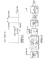
Images


Classifications
-
- H—ELECTRICITY
- H03—ELECTRONIC CIRCUITRY
- H03F—AMPLIFIERS
- H03F1/00—Details of amplifiers with only discharge tubes, only semiconductor devices or only unspecified devices as amplifying elements
- H03F1/32—Modifications of amplifiers to reduce non-linear distortion
-
- G—PHYSICS
- G05—CONTROLLING; REGULATING
- G05F—SYSTEMS FOR REGULATING ELECTRIC OR MAGNETIC VARIABLES
- G05F1/00—Automatic systems in which deviations of an electric quantity from one or more predetermined values are detected at the output of the system and fed back to a device within the system to restore the detected quantity to its predetermined value or values, i.e. retroactive systems
- G05F1/10—Regulating voltage or current
- G05F1/46—Regulating voltage or current wherein the variable actually regulated by the final control device is dc
- G05F1/56—Regulating voltage or current wherein the variable actually regulated by the final control device is dc using semiconductor devices in series with the load as final control devices
- G05F1/561—Voltage to current converters
Definitions
- This invention relates generally to voltage to current converters.
- Radio signals can include many different frequency components that are commonly referred to as channels. Usually, it is desired to select and isolate one particular channel for analog processing to be delivered to a speaker, or similar device, so that the information contained in the selected channel can be perceived by a listener as sound. In order to isolate the selected channel, radio receivers are tuned to a particular frequency, which corresponds to the selected channel.
- Tuning a radio receiver requires that circuitry within the radio receiver be configured to respond primarily to a frequency corresponding to the selected channel.
- tuning the radio receiver included tuning a narrow-band radio-frequency (RF) filter near the antenna input to filter the radio signal prior to that signal being amplified.
- the narrow filtering provided by the narrow-band filter removed essentially all frequencies from the radio signal, except for a very narrow band of frequencies around the selected channel. Passing only the frequency used for the selected channel provided for a relatively high degree of selectivity, and allowed the filtered signal to be amplified by relatively simple amplifiers.
- Narrow-band RF filters while providing good selectivity, have the disadvantage of adding expense and complexity to the radio receiver, since tuning of the narrow-band filter must be precisely coordinated with the tuning of other circuitry within the radio for optimum performance.
- the precise tuning requirements of narrow-band filters often require more parts with close tolerances, which can significantly add to the cost of building a radio receiver.
- manufacturers have more recently begun specifying that broadband filters should be used at the antenna input in place of narrow-band filters.
- FIG. 1 shows a desired signal 140, a first adjacent signal 110 and a second adjacent signal 120 which are all passed through a broadband filter.
- the broadband filtering will be centered about the wanted signal 140, and that for purposes of illustration that one or more adjacent signals will generally exist on both sides of the wanted signal 140. However, for purposes of discussion, only the adjacent signals on one side of the wanted signal 140 are illustrated. In older radio systems which employ a narrow-band filter, first adjacent signal 110 and second adjacent signal 120 would be filtered out, but this is not the case when using a broadband filter.
- a mixer with a voltage-to-current converter is presented with a radio signal that includes adjacent signals, such as first and second adjacent signals 110 and 120, third order signals 130 and 132 will be produced.
- Third order signals 130 and 132 associated with the first and second adjacent signals are unwanted artifacts produced because of non-linearities in the voltage-to-current converter that correspond to the third term in a power series equation.
- These third order signals can reside at a frequency close enough to the frequency of the wanted signal 140 to cause distortion and interference.
- Subsequent narrow band filters in the radio circuitry will filter out first adjacent signal 110, second adjacent signal 120 and third order signal 132 without too much difficulty, because these signals have frequencies that are substantially different from wanted signal 140.
- the narrow band filters may have difficulty filtering out third order signal 130, because it is so close in frequency to wanted signal 140.
- a voltage-to-current converter that can be used in conjunction with broadband input filters.
- a voltage-to-current converter could be made more linear to avoid or decrease problems with third order signals generated due to the non-linearity, while at the same time not introducing phase shift problems such as those introduced by some conventional voltage-to-current converters, degrade the overall noise figure of the receiver or use large bias currents to achieve the required linearity.
- FIGs. 2-6 illustrate a frequency modulated (FM) radio receiver and a voltage-to-current converter used therein.
- the input to the voltage-to-current converter is received from a broadband filter, which does not filter out all frequency components adjacent to a desired channel's frequency.
- the voltage-to-current converter employs a main differential amplifier and a cancellation differential amplifier to produce an output having reduced third order distortion components.
- the output of the voltage-to-current converter is fed into a mixer where the signal is mixed with a signal from a local oscillator to produce an intermediate frequency (IF) which is then filtered, amplified, and demodulated to produce an audio output.
- IF intermediate frequency
- the voltage-to-current converter described in at least one embodiment does not introduce unacceptable phase shifts nor excessive non-linearities when used in radio receivers.
- Radio 200 includes an antenna 208, a broadband input filter 210, a voltage to current converter 220, a local oscillator 232, a mixer 230, a narrow band intermediate frequency (IF) filter 240, an IF amplifier 250 and an FM demodulator 260.
- broadband input filter 210 receives a radio signal from an antenna 208.
- the radio signal received from antenna 208 includes a number of channels corresponding to particular frequencies, including a desired channel, and a number of undesired channels.
- Broadband input filter 210 filters out some of the undesired channels contained in the radio signal received from antenna 208.
- the channels filtered out by broadband input filter 210 include primarily channels corresponding to frequencies that are relatively distant from the frequency of the desired channel. However, frequency components from at least two adjacent channels are not completely filtered out by broadband input filter 210.
- the filtered radio signal is passed from broadband input filter 210 to voltage-to-current converter 220.
- Voltage-to-current converter 220 linearly converts the filtered radio signal voltage to an output current and passes the output current to mixer 230.
- voltage-to-current converter 220 employs two differential amplifiers with their outputs cross-coupled.
- Main amplifier 222 which in the illustrated embodiment is a differential. amplifier, performs a voltage-to-current conversion in a manner well known to those skilled in the art.
- Cancellation amplifier 224 which is also illustrated as a differential amplifier in FIG. 2, receives the same inputs as main amplifier 222, but the outputs of cancellation amplifier 224 are cross-coupled to the outputs of main amplifier 222. This means that the positive output of cancellation amplifier 224 is connected to the inverting output of main amplifier 222, while the inverting output of cancellation amplifier 224 is connected to the non-inverting output of main amplifier 224.
- Both main amplifier 222 and cancellation amplifier 224 have a characteristic forward tansconductance (g m ), which is essentially a measure of how much the output current of the differential amplifier changes for a given change in the input voltage.
- the g m of main amplifier 222 is configured to be significantly larger than the g m of cancellation amplifier 224. In at least one embodiment, the g m of main amplifier 222 is approximately ten times greater than the g m of cancellation amplifier 224. In other embodiments, the g m of main amplifier 224 is configured to be between about five times and fifteen times greater than the g m of cancellation amplifier 224.
- the ratio of the g m of main amplifier 222 to the g m of cancellation amplifier 224 is configured to be greater than 15:1, matching transistors within the differential amplifiers can become more of a problem. Conversely, if the ratio of the g m of main amplifier 222 to the g m of cancellation amplifier 224 is configured to be less than 5:1, significant signal loss of the wanted signal 140 may impact the effectiveness of the cross-coupling arrangement. It will be appreciated that according to the teachings set forth herein the ratio of the g m of main amplifier 222 to the g m of cancellation amplifier 224 can be configured outside the range stated herein, however it is anticipated that g m ratios lying outside of the stated ranges may be somewhat problematic.
- the amount of bias current supplied to each of the amplifiers is different.
- the bias current supplied to main amplifier 222 is greater than the amount of bias current supplied to cancellation amplifier 224.
- cancellation amplifier 224 will produce a greater relative amount of distortion than that produced by main amplifier 222.
- the g m of main amplifier 222 is configured to be greater than the g m of cancellation amplifier 224.
- the ratio of the distortion to the desired signal produced in cancellation amplifier 224 is much greater than the ratio of the distortion of the desired signal in main amplifier 222.
- the end effect is that the output of voltage-to-current converter 220 has a significantly reduced amount of third order distortion produced by the undesired signals than would main op amp 222 without the cancellation provided by cancellation amp 224.
- the process of canceling out the undesired third order distortion, without significantly lowering the amount of desired signal, will be discussed subsequently in relation to FIGs. 4-6.
- the output of voltage-to-current converter 220 which has a reduced amount of third order distortion, is then fed into mixer 230.
- Mixer 230 mixes the output of voltage-to-current converter 220 with the output of local oscillator 232 in a manner well known to those skilled in the art, to produce an intermediate frequency (IF) signal.
- IF intermediate frequency
- This IF frequency signal is used by other circuitry within radio 200 to produce the audio output.
- the output of mixer 230 which still includes a desired channel, some undesired channels in a band around the desired channel, and some small amount of third order distortion is now passed to narrow-band IF filter 240.
- Narrow band IF filter 240 removes undesired frequency components from the signal, except for any undesired frequencies that are too close to the desired channel. Recall that some third order distortion is normally close enough to the desired signal such that narrow band IF filter 240 does not completely remove it. Therefore, by the time the signal reaches narrow band IF filter 240 it is desirable that third order distortion have been previously removed or minimized so that the quality of the audio output of the radio will not be significantly affected. Recall also that due to the cross-coupling of main amplifier 222 and cancellation amplifier 224 in voltage-to-current converter 220, at least one embodiment of the present invention provides an output having a reduced amount of third order distortion.
- IF amplifier 250 After the signal leaves narrow band IF filter 240 it is fed into an IF amplifier 250.
- IF amplifier 250 amplifies the IF signal and provides it to an FM demodulator 260.
- the FM demodulator 260 separates the information in the signal from the carrier, and then processes the information into an audio output signal that can be delivered to speakers, equalizers, or other suitable signal handling circuitry or equipment (not shown).
- FIG. 3 an embodiment of a voltage-to-current converter according to one embodiment of the present invention is illustrated and designated generally as converter 300.
- the input to converter 300 is Vin, which in at least one embodiment is the output of a broadband radio frequency filter as discussed in FIG. 2.
- the transistors outside of the dotted line, Q1, Q2, Q3 and Q4 form main differential amplifier 360, and the transistors inside of the dotted lines, Q11, Q12, Q13 and Q14 form cancellation amplifier 350.
- Transistors Q3 and Q4, along with resistors RB1, form constant current tails for main amplifier 360, while transistors Q13, Q14 and resistors RB2 form constant current tails for cancellation amplifier 350.
- Constant current tails are well known to those skilled in the art, and so the following discussion will focus primarily on transistors Q1, Q2, Q11, Q12 and resistors RE2 and RE1. Proper biasing of the illustrated transistors using bias voltages VB is also well understood by those skilled in the art.
- the g m of main amplifier 360 should be set to be greater than the g m of cancellation amplifier 350.
- the g m of main amplifier 360 is primarily governed by the value of resistor RE1, while the gain of cancellation amplifier 350 is primarily controlled by the value of resistor RE2.
- main amplifier 360 which includes transistors Q and Q2, is configured to have a g m approximately ten times greater than the g m of cancellation amplifier 350, which includes transistors Q11 and Q12. To understand why this is necessary, consider the case where the g m of main amplifier 360 is the same as the g m of cancellation amplifier 350.
- output current IO1 which is the sum of collector current IC1 from transistor Q1 and collector current IC12 from transistor Q12
- output current IO2 is the sum of collector current IC2 from transistor Q2 and IC11 from transistor Q11, and will also have a non-zero value, but will be 180 degrees out of phase with IO1. Note that as long as the ratio of g m between main amplifier 260 (which includes transistors Q1 and Q2) and cancellation amplifier 350 (which includes transistors Q11 and Q12) is greater than about 5:1, the amount of signal lost due to the cross-coupling should not significantly adversely affect the operation of converter 300.
- the values of RE2 and RE1 are set to have a ratio of approximately 10:1, and the values of RB1 and RB2 are chosen to match the magnitude of the third level distortion components produced by main amplifier 360 and cancellation amplifier 350.
- the value of RB2 effectively sets the amount of bias current that flows through transistors Q11 and Q12, while the value of RB1 effectively sets the amount of bias current that flows through transistors Q1 and Q2.
- the value RB2 By making the value RB2 higher than the value of RB1, the amount of bias current in Q11 and Q12 is made correspondingly smaller than the amount of bias current that flows through transistors Q1 and Q2, thus increasing third order distortion in cancellation amplifier 350.
- the third order distortion in cancellation amplifier 350 can be increased until it is equal in magnitude to the third order distortion in amplifier 360.
- the g m of cancellation amplifier 350 is still much less than the g m of main amplifier 360 because the value of RE2 is much greater than the value of RE1.
- the ratio of resistors RB1 to RB2 which is selected to be consistent with the ration of RE1 to RE2, also plays a role in increasing the amount of distortion in cancellation amplifier 350 over the amount of distortion produced by main amplifier 360.
- RB1 has a smaller value that RB2, more current flows through transistors Q 1 and Q2 than flows through transistors Q11 and Q12.
- a decrease in the amount of current flowing through a transistor increases the amount of third order distortion produced by a transistor. Therefore, the reduced amount of current flowing through transistors Q11 and Q12 increases the distortion generated by cancellation op amp 350 as compared to the amount of distortion produced by main amplifier 360.
- the amount of current flowing through transistors Q11 and Q12 is approximately 18 times less than the amount of current flowing through transistors Q1 and Q2.
- FIG. 3 illustrates conventional bi-polar junction transistors (BJT), other transistors such as field effect transistors (FET) and the like may be used in implementing a converter according to the principles discussed herein.
- BJT bi-polar junction transistors
- FET field effect transistors
- converter 300 shows the outputs of a main amplifier 360 and a cancellation amplifier 350 as being cross-coupled, in other embodiments the inputs of a main amplifier and a cancellation amplifier may be cross-coupled, while the outputs are coupled in parallel, thereby achieving the same or similar effect as that discussed with respect to FIG. 3.
- FIG. 4 shows the generation of third order frequency peak 430 due to amplification of two separate frequency peaks 410 and 420 by a non-linear amplifier.
- the desired signal was not included in the illustrated simulation, nor were additional undesired frequencies on the other side of the desired signal. If the desired signal were included in the simulation, it would be at the same frequency as third order frequency peak 430, and have the same amplitude as frequency peaks 410 and 420.
- the two frequency peaks 410 and 420 which represent undesired frequencies have an amplitude of approximately -14 db.
- peak 430 is approximately -85 db.
- the difference between frequency peaks 410 and 420 and third order frequency peak 430 is approximately 70 dB.
- the desired signal (not shown) will have an amplitude of approximately the same as the undesired signals and therefore the difference between the amplitude of a desired signal and third order frequency peak 430 as shown in FIG. 4 will also be approximately 70 db.
- Undesired frequency peaks 510 and 520 have a maximum value of approximately -35 dB while distortion peak 530 has a value of approximately -85 dB.
- the difference in amplitude between undesired frequency peaks 510 and 520 and distortion peak 530 is approximately 50 dB, as compared to a difference of approximately 70 dB in the main differential amplifier (see FIGS. 3 and 4) without any cancellation applied.
- the desired signal not shown
- the output of the cancellation differential amplifier generates a higher ratio of third order distortion to desired signal than does the main differential amplifier (see FIG. 4).
- FIG. 6 shows, in effect, the output of a cancellation amplifier illustrated in FIG. 5 subtracted from the output of a main amplifier shown in FIG. 4.
- third order distortion 530 (FIG. 5) which is the output of a cancellation amplifier
- third order distortion 430 (FIG. 4) which is the output of a main differential amplifier
- the magnitude of combined third order distortion 630 is approximately-115 dB, whereas the distortion of the main amplifier without a cancellation amplifier was approximately -85 dbs.
- the third order distortion has been improved by approximately 30 db.
- the amplitude of frequency peaks 610 and 620 is approximately -15 dB, which is only about one dB less than the magnitude of frequency peaks 410 and 420 (FIG. 4). It is apparent, therefore, that by using the cancellation differential amplifier in the manner disclosed herein, the third order distortion of an output signal from a voltage to current converter, is significantly reduced, but there is no corresponding significant reduction in the output of other frequency peaks. Maintaining the assumption that the magnitude of the desired frequency peak (not shown) is approximately the same as the magnitude of the undesired frequency peaks 610 an 620, it should be clear that it will be much easier for subsequent circuitry to distinguish between the desired frequency peak (not shown) and third order distortion peak 630, than would have been otherwise possible.
- the distortion produced by the cancellation amplifier can be used to cancel out some of the distortion in the main amplifier without seriously degrading the amplitude of the desired signal.
Landscapes
- Engineering & Computer Science (AREA)
- Physics & Mathematics (AREA)
- Electromagnetism (AREA)
- General Physics & Mathematics (AREA)
- Radar, Positioning & Navigation (AREA)
- Automation & Control Theory (AREA)
- Nonlinear Science (AREA)
- Power Engineering (AREA)
- Amplifiers (AREA)
- Noise Elimination (AREA)
Applications Claiming Priority (2)
| Application Number | Priority Date | Filing Date | Title |
|---|---|---|---|
| US10/160,348 US6798289B2 (en) | 2002-05-31 | 2002-05-31 | System, apparatus and method for voltage to current conversion |
| US160348 | 2002-05-31 |
Publications (2)
| Publication Number | Publication Date |
|---|---|
| EP1376293A2 true EP1376293A2 (de) | 2004-01-02 |
| EP1376293A3 EP1376293A3 (de) | 2005-02-09 |
Family
ID=29583124
Family Applications (1)
| Application Number | Title | Priority Date | Filing Date |
|---|---|---|---|
| EP03012321A Withdrawn EP1376293A3 (de) | 2002-05-31 | 2003-05-29 | System, Vorrichtung und Verfahren für Spannung-Strom-Wandlung |
Country Status (3)
| Country | Link |
|---|---|
| US (1) | US6798289B2 (de) |
| EP (1) | EP1376293A3 (de) |
| KR (1) | KR20030094052A (de) |
Families Citing this family (3)
| Publication number | Priority date | Publication date | Assignee | Title |
|---|---|---|---|---|
| US7403758B2 (en) * | 2005-10-04 | 2008-07-22 | Freescale Semicondutor, Inc. | Linearized and balanced mixer apparatus and signal mixing method |
| US9136787B2 (en) * | 2012-10-25 | 2015-09-15 | Texas Instruments Incorporated | Back EMF monitor for motor control |
| IT202000004159A1 (it) * | 2020-02-28 | 2021-08-28 | St Microelectronics Srl | Convertitore tensione-corrente, dispositivo e procedimento corrispondenti |
Citations (3)
| Publication number | Priority date | Publication date | Assignee | Title |
|---|---|---|---|---|
| US4390848A (en) * | 1981-02-12 | 1983-06-28 | Signetics | Linear transconductance amplifier |
| US4749957A (en) * | 1986-02-27 | 1988-06-07 | Yannis Tsividis | Semiconductor transconductor circuits |
| EP0324273A2 (de) * | 1988-01-13 | 1989-07-19 | Tektronix, Inc. | Breitbandig linearisierter emitterrückgekoppelter Verstärker |
Family Cites Families (5)
| Publication number | Priority date | Publication date | Assignee | Title |
|---|---|---|---|---|
| US4147971A (en) * | 1977-08-22 | 1979-04-03 | Motorola, Inc. | Impedance trim network for use in integrated circuit applications |
| US4555673A (en) * | 1984-04-19 | 1985-11-26 | Signetics Corporation | Differential amplifier with rail-to-rail input capability and controlled transconductance |
| EP0352009B1 (de) * | 1988-07-18 | 1994-11-17 | Sony Corporation | Verstärkerschaltung |
| CA2163559C (en) * | 1994-04-04 | 2000-11-07 | Thomas A. Freeburg | A wide bandwidth discriminator for use in a radio receiver |
| DE69426650T2 (de) * | 1994-11-07 | 2001-09-06 | Alcatel Sa | Mischer für Sender, mit einem Eingang im Strom-Modus |
-
2002
- 2002-05-31 US US10/160,348 patent/US6798289B2/en not_active Expired - Lifetime
-
2003
- 2003-05-29 EP EP03012321A patent/EP1376293A3/de not_active Withdrawn
- 2003-05-30 KR KR10-2003-0034754A patent/KR20030094052A/ko not_active Application Discontinuation
Patent Citations (3)
| Publication number | Priority date | Publication date | Assignee | Title |
|---|---|---|---|---|
| US4390848A (en) * | 1981-02-12 | 1983-06-28 | Signetics | Linear transconductance amplifier |
| US4749957A (en) * | 1986-02-27 | 1988-06-07 | Yannis Tsividis | Semiconductor transconductor circuits |
| EP0324273A2 (de) * | 1988-01-13 | 1989-07-19 | Tektronix, Inc. | Breitbandig linearisierter emitterrückgekoppelter Verstärker |
Also Published As
| Publication number | Publication date |
|---|---|
| US6798289B2 (en) | 2004-09-28 |
| EP1376293A3 (de) | 2005-02-09 |
| US20030222714A1 (en) | 2003-12-04 |
| KR20030094052A (ko) | 2003-12-11 |
Similar Documents
| Publication | Publication Date | Title |
|---|---|---|
| US8594603B2 (en) | Systems and methods for cancelling interferers in a receiver | |
| US4907293A (en) | Adjacent channel interference suppressing system for FM receiver | |
| US7146141B2 (en) | Direct conversion receiver with DC offset compensation and method thereof | |
| US20060001489A1 (en) | Highly linear variable gain amplifier | |
| JP3190551B2 (ja) | マルチキャリア信号の処理方法及び装置 | |
| JP2001044860A (ja) | 自動利得制御回路を有する受信器 | |
| US7403760B1 (en) | DC offset correction for direct-conversion receiver | |
| KR910000686B1 (ko) | 주파수콘버터 | |
| KR100687012B1 (ko) | 주파수 변환장치와 이를 포함하는 수신기 및 주파수 변환방법 | |
| JP3177388B2 (ja) | 無線フロントエンド装置 | |
| US7493097B2 (en) | High dynamic range compact mixer output stage for a wireless receiver | |
| EP1376293A2 (de) | System, Vorrichtung und Verfahren für Spannung-Strom-Wandlung | |
| TW200308141A (en) | Amplifier and radio frequency tuner | |
| US6137359A (en) | Low-distortion high-frequency amplifier | |
| US5151939A (en) | Adaptive audio processor for am stereo signals | |
| EP1385268B1 (de) | Digital-Analog Wandler | |
| CA1246151A (en) | Autodyne receiver | |
| US4404431A (en) | AM Stereo receiver | |
| KR101374855B1 (ko) | 증폭기에서의 고조파 및 혼변조 왜곡제거 장치 및 방법 | |
| US5942939A (en) | Amplifier and method of canceling distortion by combining hyperbolic tangent and hyperbolic sine transfer functions | |
| US4146842A (en) | Noise muting circuit in fm receiver | |
| JPH11289240A (ja) | 調節可能な高域通過フィルタ用回路装置 | |
| JPH0752851B2 (ja) | Fm受信装置 | |
| JP2006513615A (ja) | 一定の入力インピーダンスを有する制御可能なrf広帯域増幅器 | |
| JPS60212038A (ja) | 受信機 |
Legal Events
| Date | Code | Title | Description |
|---|---|---|---|
| PUAI | Public reference made under article 153(3) epc to a published international application that has entered the european phase |
Free format text: ORIGINAL CODE: 0009012 |
|
| AK | Designated contracting states |
Kind code of ref document: A2 Designated state(s): AT BE BG CH CY CZ DE DK EE ES FI FR GB GR HU IE IT LI LU MC NL PT RO SE SI SK TR |
|
| AX | Request for extension of the european patent |
Extension state: AL LT LV MK |
|
| RAP1 | Party data changed (applicant data changed or rights of an application transferred) |
Owner name: FREESCALE SEMICONDUCTOR, INC. |
|
| PUAL | Search report despatched |
Free format text: ORIGINAL CODE: 0009013 |
|
| AK | Designated contracting states |
Kind code of ref document: A3 Designated state(s): AT BE BG CH CY CZ DE DK EE ES FI FR GB GR HU IE IT LI LU MC NL PT RO SE SI SK TR |
|
| AX | Request for extension of the european patent |
Extension state: AL LT LV MK |
|
| 17P | Request for examination filed |
Effective date: 20050809 |
|
| AKX | Designation fees paid |
Designated state(s): DE FR GB IT |
|
| STAA | Information on the status of an ep patent application or granted ep patent |
Free format text: STATUS: THE APPLICATION IS DEEMED TO BE WITHDRAWN |
|
| 18D | Application deemed to be withdrawn |
Effective date: 20091201 |