EP1365447A2 - Manufacturing method of semiconductor substrate - Google Patents
Manufacturing method of semiconductor substrate Download PDFInfo
- Publication number
- EP1365447A2 EP1365447A2 EP03010842A EP03010842A EP1365447A2 EP 1365447 A2 EP1365447 A2 EP 1365447A2 EP 03010842 A EP03010842 A EP 03010842A EP 03010842 A EP03010842 A EP 03010842A EP 1365447 A2 EP1365447 A2 EP 1365447A2
- Authority
- EP
- European Patent Office
- Prior art keywords
- ions
- sige layer
- substrate
- layer
- silicon
- Prior art date
- Legal status (The legal status is an assumption and is not a legal conclusion. Google has not performed a legal analysis and makes no representation as to the accuracy of the status listed.)
- Withdrawn
Links
Images


Classifications
-
- H—ELECTRICITY
- H10—SEMICONDUCTOR DEVICES; ELECTRIC SOLID-STATE DEVICES NOT OTHERWISE PROVIDED FOR
- H10P—GENERIC PROCESSES OR APPARATUS FOR THE MANUFACTURE OR TREATMENT OF DEVICES COVERED BY CLASS H10
- H10P10/00—Bonding of wafers, substrates or parts of devices
-
- H—ELECTRICITY
- H10—SEMICONDUCTOR DEVICES; ELECTRIC SOLID-STATE DEVICES NOT OTHERWISE PROVIDED FOR
- H10P—GENERIC PROCESSES OR APPARATUS FOR THE MANUFACTURE OR TREATMENT OF DEVICES COVERED BY CLASS H10
- H10P90/00—Preparation of wafers not covered by a single main group of this subclass, e.g. wafer reinforcement
- H10P90/19—Preparing inhomogeneous wafers
- H10P90/1904—Preparing vertically inhomogeneous wafers
- H10P90/1906—Preparing SOI wafers
-
- H—ELECTRICITY
- H10—SEMICONDUCTOR DEVICES; ELECTRIC SOLID-STATE DEVICES NOT OTHERWISE PROVIDED FOR
- H10W—GENERIC PACKAGES, INTERCONNECTIONS, CONNECTORS OR OTHER CONSTRUCTIONAL DETAILS OF DEVICES COVERED BY CLASS H10
- H10W10/00—Isolation regions in semiconductor bodies between components of integrated devices
- H10W10/01—Manufacture or treatment
- H10W10/061—Manufacture or treatment using SOI processes together with lateral isolation, e.g. combinations of SOI and shallow trench isolations
-
- H—ELECTRICITY
- H10—SEMICONDUCTOR DEVICES; ELECTRIC SOLID-STATE DEVICES NOT OTHERWISE PROVIDED FOR
- H10W—GENERIC PACKAGES, INTERCONNECTIONS, CONNECTORS OR OTHER CONSTRUCTIONAL DETAILS OF DEVICES COVERED BY CLASS H10
- H10W10/00—Isolation regions in semiconductor bodies between components of integrated devices
- H10W10/10—Isolation regions comprising dielectric materials
- H10W10/181—Semiconductor-on-insulator [SOI] isolation regions, e.g. buried oxide regions of SOI wafers
-
- H—ELECTRICITY
- H10—SEMICONDUCTOR DEVICES; ELECTRIC SOLID-STATE DEVICES NOT OTHERWISE PROVIDED FOR
- H10P—GENERIC PROCESSES OR APPARATUS FOR THE MANUFACTURE OR TREATMENT OF DEVICES COVERED BY CLASS H10
- H10P90/00—Preparation of wafers not covered by a single main group of this subclass, e.g. wafer reinforcement
- H10P90/19—Preparing inhomogeneous wafers
- H10P90/1904—Preparing vertically inhomogeneous wafers
- H10P90/1906—Preparing SOI wafers
- H10P90/1908—Preparing SOI wafers using silicon implanted buried insulating layers, e.g. oxide layers [SIMOX]
-
- H—ELECTRICITY
- H10—SEMICONDUCTOR DEVICES; ELECTRIC SOLID-STATE DEVICES NOT OTHERWISE PROVIDED FOR
- H10W—GENERIC PACKAGES, INTERCONNECTIONS, CONNECTORS OR OTHER CONSTRUCTIONAL DETAILS OF DEVICES COVERED BY CLASS H10
- H10W10/00—Isolation regions in semiconductor bodies between components of integrated devices
- H10W10/01—Manufacture or treatment
- H10W10/011—Manufacture or treatment of isolation regions comprising dielectric materials
- H10W10/014—Manufacture or treatment of isolation regions comprising dielectric materials using trench refilling with dielectric materials, e.g. shallow trench isolations
-
- H—ELECTRICITY
- H10—SEMICONDUCTOR DEVICES; ELECTRIC SOLID-STATE DEVICES NOT OTHERWISE PROVIDED FOR
- H10W—GENERIC PACKAGES, INTERCONNECTIONS, CONNECTORS OR OTHER CONSTRUCTIONAL DETAILS OF DEVICES COVERED BY CLASS H10
- H10W10/00—Isolation regions in semiconductor bodies between components of integrated devices
- H10W10/10—Isolation regions comprising dielectric materials
- H10W10/17—Isolation regions comprising dielectric materials formed using trench refilling with dielectric materials, e.g. shallow trench isolations
Definitions
- the present invention relates to a manufacturing method of a semiconductor substrate.
- the present invention relates to a manufacturing method of a semiconductor substrate that is effective in gaining a high quality silicon substrate wherein distortion of silicon is utilized.
- Figs 3(a) to 3(e) The technology shown in Figs 3(a) to 3(e) is cited as an example of a manufacturing technology for a MOSFET wherein distortion is utilized.
- a SiGe layer 2 is grown in an epitaxial manner to have a thickness of approximately 300 nm and to have a concentration of Ge of 20 atom% on a silicon substrate 1 and a Si layer 3 is sequentially grown in an epitaxial manner to have a thickness of approximately 20 nm on the SiGe layer.
- the procedure passes through a conventional STI (Shallow Trench Isolation) process so that element isolation regions 11 are formed and, furthermore, as shown in Fig 3(e), a gate insulating film 12, a gate electrode 13 and source/drain regions 14 are formed according to a general manufacturing process so that a MOSFET is completed.
- STI Shallow Trench Isolation
- the amount of implantation of hydrogen ions is set at an amount of implantation lower than the amount that completely relaxes SiGe layer 2 and, thereby, prevention of the occurrence of threading dislocations 6 due to micro voids 4 of hydrogen in the subsequent heat treatment is attempted.
- the procedure passes through a conventional STI process as shown in Figs 3(c) and 3(d) under such conditions so that a MOSFET is fabricated and, then, many threading dislocations 6 are found beneath source/drain regions 14 as shown in Fig 3(e) wherein the leakage current increases at the time when a reverse voltage is applied to these junctions and, therefore, there is a problem wherein a manufacturing technology for a high quality MOSFET cannot be established.
- the present invention is provided in view of the above described problem and a purpose thereof is to provide a manufacturing method of a semiconductor device wherein threading dislocations 6 can be relaxed so that the junction leakage current can be restricted to the minimum even in the case wherein threading dislocations 6 occur starting from the interface between SiGe layer 2 and silicon substrate 1.
- the present invention provides a manufacturing method of a semiconductor substrate comprising the steps of: (a) forming a SiGe layer on a substrate of which the surface is made of silicon; (b) further forming a semiconductor layer on the SiGe layer; and (c) implanting ions into regions of the SiGe layer in the substrate that become element isolation formation regions, and carrying out a heat treatment.
- Step (a) a SiGe layer is formed on a substrate of which the surface is made of silicon.
- the substrate of which the surface is made of silicon may be a silicon substrate made of amorphous silicon, microcrystal silicon, single crystal silicon, polycrystal silicon or silicon wherein two, or more, of these crystal conditions are mixed or may be a so-called SOI substrate having such a silicon layer on the surface.
- a single crystal silicon substrate is preferable.
- the SiGe layer can be formed according to a variety of conventional methods such as, for example, a CVD method, a sputter method, a vacuum deposition method or an MEB method. In particular, it is preferable to form the SiGe layer according to an epitaxial growth method by means of a CVD method.
- the film formation conditions in this case can be selected from the conditions known in the field of the art and, in particular, a film formation temperature of, for example, from 400°C to 900°C, preferably from approximately 400°C to 650°C, is appropriate.
- the film formation temperature it is preferable for the film formation temperature to be 500°C, or below, in the case wherein a SiGe layer is grown to have a concentration of Ge in the range described below, for example, a SiGe layer is grown to have a concentration of Ge of 30 atom%.
- the concentration of Ge in this SiGe layer is not specifically limited and, for example, a concentration of from approximately 10 atom% to 50 atom%, preferably, from 10 atom% to 40 atom%, more preferably, from 20 atom% to 30 atom%, can be cited.
- the SiGe layer is a thick film so that shift dislocations at the interface between the SiGe layer and the silicon substrate that occur in a subsequent annealing step for relaxation of distortion do not negatively affect a semiconductor device, for example a MOSFET, that may be formed on top of the above.
- the lowering of the growth temperature is effective as a technique for increasing film thickness.
- the film it is preferable for the film to have a film thickness that is thinner than the film thickness wherein relaxation of lattice distortion in an SiGe layer occurs when the SiGe layer is deposited on the substrate, that is to say, to have a film thickness that is thinner than the critical film thickness.
- a thickness of from approximately 50 nm to 500 nm can be cited and, furthermore, a thickness of from approximately 100 nm to 500 nm is appropriate.
- the SiGe layer it is preferable for the SiGe layer to have a film thickness of 300 nm, or greater, taking into consideration the formation of a PN junction in a subsequent step.
- a semiconductor layer is formed on the gained substrate.
- the semiconductor layer is not specifically limited as long as it has a diamond structure in the same manner as silicon.
- Si Si to which C has been added or a SiGe layer having a concentration of Ge that is lower than that in the above described SiGe layer, for example, can be cited as the semiconductor layer.
- a silicon (Si) layer is preferable.
- the concentration of C in SiC is not specifically limited and a concentration of from approximately 0.1 atom% to 2 atom%, for example, can be cited.
- it is appropriate for the concentration of Ge in the SiGe to be approximately 10 atom%, or less.
- the semiconductor layer can be formed according to the same method as is the SiGe layer and it is preferable for the semiconductor layer to be formed within the same device after the formation of the SiGe layer by, for example, switching the growth gases. Thereby, oxygen pollution, or the like, on the surface of the SiGe layer can be reduced. It is preferable for the temperature of the substrate in this case to be from approximately 400°C to 650°C.
- the film thickness of the semiconductor layer is a thick film, taking into consideration the reduction in the film thickness in subsequent manufacturing steps for the semiconductor device as well as diffusion of Ge from the SiGe layer, and the like, while it is preferable for the semiconductor layer to be formed so as to have a film thickness less than the critical film thickness in order to suppress the occurrence of defects on the Si layer caused by distortion due to stretching after the step of relaxation of distortion of the SiGe layer.
- the film thickness is from approximately 1 nm to 100 nm and, more preferably, from approximately 5 nm to 30 nm, and, in particular, it is appropriate for the film thickness to be approximately 20 nm, or less, in the case wherein the semiconductor layer is formed on a SiGe layer having a concentration of Ge of 30 atom% and it is appropriate for the film thickness to be approximately 50 nm, or less, in the case of a concentration of Ge of 20 atom%.
- ions into the gained substrate and to carry out a heat treatment after the formation of the SiGe layer and after the formation of the semiconductor layer.
- ion implantation using elements that can introduce lattice defects in the surface of the utilized silicon substrate as well as elements that can create micro cavities in the silicon substrate as a result of annealing after ion implantation, or the like, and such elements can be selected from the group consisting of hydrogen, inert gases and elements of group IV. Concretely, hydrogen, helium, neon, silicon, carbon, germanium, and the like can be cited as such elements and, in particular, hydrogen is preferable.
- the acceleration energy for ion implantation can be appropriately adjusted depending on the type of used ions, the film thickness of the SiGe layer, the material and film thickness of the semiconductor layer, and the like. It is desirable to set the acceleration energy at a value, for example, wherein the implantation peak is located at a position in the silicon substrate in the vicinity of the interface between the SiGe layer and the substrate and, more concretely, wherein the peak is located at a depth of approximately 20 nm, or greater, (preferably at a depth of from approximately 30 nm to 70 nm) in the substrate from the interface in order to prevent defects in the SiGe layer and in order to prevent the SiGe layer from becoming a thin film.
- a dose value of approximately 2 ⁇ 10 16 cm -2 , or less, can be cited.
- Furnace annealing, lamp annealing, RTA, and the like can be cited as types of annealing that can be carried out in an inert gas atmosphere, in a standard atmosphere, in a nitrogen gas atmosphere, in an oxygen gas atmosphere, in a hydrogen gas atmosphere, or the like, at a temperature in a range of from 600°C to 900°C for from approximately 10 minutes to 30 minutes.
- ions are implanted into regions of the SiGe layer on the substrate that become element isolation formation regions and a heat treatment is carried out.
- the implanted ions can be selected, for example, from the group comprising of hydrogen, inert gases and elements of groups II to V.
- ions of hydrogen, helium, neon, silicon, carbon, germanium, arsenic, phosphorous, boron, and the like can be cited and, in particular, silicon ions, germanium ions, arsenic ions, and the like, are preferable wherein silicon ions are more preferable.
- the acceleration energy for ion implantation can be appropriately adjusted depending on the type of used ions, the film thickness of the SiGe layer, the material and film thickness of the semiconductor layer, and the like. It is preferable to set the acceleration energy, for example, at a value wherein the implantation peak is located in an upper portion of the SiGe layer and, more concretely, wherein the peak is located at a position of the SiGe layer approximately 20 nm above the interface. A value of from approximately 20 keV to 150 keV, for example, can be cited as the implantation energy. A dose value of approximately 1 ⁇ 10 15 cm -2 , or greater, for example, can be cited.
- trenches of which the bottoms are located in the SiGe layer, in regions that become element isolation formation regions before the ion implantation in the above step so that ions are implanted into the bottoms of these trenches.
- Trenches can be created according to a well-known photolithographic and etching process.
- etching may be by anisotropic or isotropic etching or by dry or wet etching, and anisotropic etching is preferable.
- the size and form of trenches are not specifically limited and can be appropriately adjusted in accordance with the design of the semiconductor device that is desired to be gained.
- the depth of trenches can be appropriately adjusted depending on the film thickness, or the like, of the SiGe layer and a depth of from approximately 200 nm to 450 nm can be cited.
- the heat treatment can be carried out according to the same method as described above.
- the temperature it is preferable for the temperature to be set at from approximately 550°C to 650°C.
- SiGe layer 2 is grown in an epitaxial manner to have a thickness of approximately 300 nm and to have a concentration of Ge of 30 atom% using a well-known CVD (Chemical Vapor Deposition) method at a temperature of from 400°C to 900°C in an atmosphere of a mixed gas of SiH 4 and GeH 4 diluted with a hydrogen gas on the surface of a p type Si single crystal substrate (hereinafter referred to as silicon substrate 1) in the plane direction (100) having a concentration of doped boron of approximately 1 ⁇ 10 15 cm -3 that is used in a conventional Si manufacturing process.
- CVD Chemical Vapor Deposition
- Si semiconductor layer 3 is grown in an epitaxial manner to have a thickness of approximately 20 nm on SiGe layer 2 using a CVD method at a temperature of from 400°C to 900°C wherein the growth gas is switched to a SiH 4 gas diluted with a hydrogen gas utilizing the same manufacturing unit.
- a dose of hydrogen ions of 2 ⁇ 10 16 cm -2 , or less, is implanted using an implantation energy of from 30 keV to 35 keV and, after that, a heat treatment is carried out at a temperature of 600°C, or higher.
- the positions wherein micro voids 4 of the hydrogen ions are created correspond to the position of the implantation peak and threading dislocations 6, which have reached to the inner surfaces of the stacking faults that have occurred due to a factor other than the hydrogen at this time, are thermodynamically stable and remain until the final step, in the case wherein there are no elimination sites, so as to cause leakage from a PN junction and, therefore, it is necessary to reduce such threading dislocations.
- a well-known photolithographic technology is used to form a resist pattern 7 for the formation of element isolation regions and this resist pattern (resist as an etching mask) 7 is used to etch SiGe layer 2 and Si layer 3 to a depth of 350 nm by means of a well-known RIE (Reactive Ion Etching) method using a SF 6 gas and, thereby, trenches 8 for element isolation are created.
- RIE Reactive Ion Etching
- a dose of Si ions of 1 ⁇ 10 15 cm -2 is implanted into the bottoms of trenches 8 for element isolation using an implantation energy of 40 KeV by means of a well-known ion implantation method.
- a heat treatment is carried out at the comparatively low temperature of approximately 600°C and, thereby, stacking faults 9 are created in the bottoms of trenches 8 for element isolation.
- the amount of the implantation of the Si ions is 1 ⁇ 10 15 cm -2 , or greater, in order to convert SiGe layer 2 into an amorphous layer and the conditions concerning the implantation energy are selected so that the implantation peak is 20 nm, or greater, in order to form nuclei of stacking faults.
- the annealing temperature is set at 600°C in the case of utilization of SiGe so that recovery from damage can progress and nuclei can be formed.
- trenches 8 for element isolation are filled in with SiO 2 , which is formed of a SiH 4 gas and an O 2 gas by means of a well-known CVD method and, then, flattening is carried out by removing the SiO 2 film from regions other than the element isolation regions by means of a well-known CMP (Chemical Mechanical Polishing) method so that element isolation regions 11 are formed.
- SiO 2 is formed of a SiH 4 gas and an O 2 gas by means of a well-known CVD method and, then, flattening is carried out by removing the SiO 2 film from regions other than the element isolation regions by means of a well-known CMP (Chemical Mechanical Polishing) method so that element isolation regions 11 are formed.
- CMP Chemical Mechanical Polishing
- a SiO 2 film may be formed by means of the well-known CVD method and, next, a SiN film may be formed in an atmosphere of SiH 4 and NH 3 by means of the well-known CVD method after the step of Fig 1(b) in order to increase the process margin for the etching of the SiO 2 according to the above described CMP method.
- the SiN film is used to stop the etching at the time of the CMP.
- a heat treatment is carried out at a temperature of from 800°C to 1000°C.
- the threading dislocations 6 in the active regions in Fig 1(c) can be shifted towards stacking faults 9 created in Fig 1(d) so as to be trapped in stacking faults 9.
- These trapped dislocations 10 are thermally stable and are not released again as a result of the heat treatment at a temperature of 1000°C, or below, that is subsequently carried out in the Si manufacturing process.
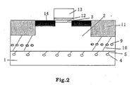
- a gate insulating film 12 a gate electrode made of an N type polycrystal Si film and N type source/drain regions 14 are formed according to a well-known MOSFET manufacturing technology so that the MOSFET is completed.
- SiGe layer 2 which has a thickness of 300 nm
- Si layer 3 which has a thickness of 20 nm
- gate electrode 13 is formed above the Si layer with gate insulating film 12 intervened in the semiconductor device manufactured in the above described manner, as shown in Fig 2.
- Source/drain regions 14 are formed on both sides of gate electrode 13 and a channel region is formed in SiGe layer 2 directly beneath gate electrode 13 between source/drain regions 14. This semiconductor device is isolated from other elements by means of trench-type element isolation regions 11.
- micro voids 4 are created at a depth of approximately 50 nm from the interface between SiGe layer 2 and silicon substrate 1 and stacking faults (dislocations) 5 that develop from these micro voids 4 extend to the interface between SiGe layer 2 and silicon substrate 1 so as to relax the majority of the distortion in SiGe layer 2.
- stacking faults 9 are created beneath element isolation regions 11 wherein dislocations 10 occurring due to the relaxation of the distortion in SiGe layer 2 are captured by these stacking faults 9.
- relaxation of the distortion at the interface between the silicon substrate and the SiGe layer is promoted and, at the same time, stacking faults that occur due to shift at the SiGe/Si interface can be prevented by utilizing the stacking faults that develop from microscopic defects by means of a heat treatment after the relaxation of distortion due to hydrogen ion implantation.
- an amount of ions smaller than an amount that will completely relax the SiGe layer is implanted and a heat treatment is carried out so that stacking faults that have developed from the interface between the SiGe layer and the silicon layer also partially relax the SiGe layer.
- the stacking faults that have developed from the interface between the SiGe layer and the silicon layer and that have reached the surface shift in a thermally random manner in the direction perpendicular to the surface of the substrate when the temperature is raised. Therefore, according to the present invention, the stacking faults are shifted toward the element isolation regions that cover the periphery of a normally active region so that dislocations are erased therein.
- an excessive amount of silicon ions is introduced into the silicon substrate by means of an ion implantation method so that stacking faults that occur at the time when a device is formed at a comparatively low temperature are utilized.
- the dislocations that have once been captured by these stacking faults are converted to a stable condition with respect to energy and, therefore, most of these dislocations do not shift toward the active region during heat treatment in a conventional manufacturing process for a transistor and, therefore, no problems are caused.
- dislocations in an active region which cause problems in the case wherein a high speed MOSFET is formed using a provisional substrate including SiGe, are trapped beneath element isolation regions so that the active region is not negatively affected and, thereby, a semiconductor substrate can be manufactured wherein junction leakage, which has conventionally been problematic, can be greatly reduced. It becomes possible by utilizing such a semiconductor substrate to implement a high speed LSI that requires a low consumption of power and that cannot conventionally be manufactured using distorted Si.
Landscapes
- Insulated Gate Type Field-Effect Transistor (AREA)
- Element Separation (AREA)
- Recrystallisation Techniques (AREA)
Abstract
Description
Claims (20)
- A manufacturing method of a semiconductor substrate comprising the steps of: (a) forming a SiGe layer on a substrate of which the surface is made of silicon; (b) further forming a semiconductor layer on the SiGe layer; and (c) implanting ions into regions of the SiGe layer in the substrate that become element isolation formation regions, and carrying out a heat treatment.
- The method according to Claim 1, wherein the ions implanted in Step (c) are selected from the group consisting of hydrogen, inert gases and elements of groups II to V and the dose of the ions is 1 × 1015 cm-2, or greater.
- The method according to Claim 2, wherein the ions are silicon ions, germanium ions or arsenic ions.
- The method according to Claim 1, wherein trenches of which the bottoms are located in the SiGe layer are created in the regions that become the element isolation formation regions before the ion implantation of Step (c) so that the ions are implanted in the bottoms of the trenches in Step (c).
- The method according to Claim 1, wherein the SiGe layer is formed so as to have a concentration of Ge of from 10 atom% to 50 atom% and so as to have a film thickness of from 50 nm to 500 nm.
- The method according to Claim 1, wherein the semiconductor layer is a SiGe layer with a concentration of Ge lower than in the Si and SiGe layers to which Si or C has been added.
- The method according to Claim 1, wherein the semiconductor substrate is used for a MOS transistor.
- A manufacturing method of a semiconductor substrate comprising the steps of: (a) forming a SiGe layer on a substrate of which the surface is made of silicon; (b) further forming a semiconductor layer on the SiGe layer; (c) implanting ions into regions of the SiGe layer in the substrate which become element isolation formation regions and carrying out a heat treatment; and (d) implanting ions into the substrate and carrying out a heat treatment, wherein Step (d) is carried out after Steps (a) and (b) and before Step (c).
- The method according to Claim 8, wherein the ions implanted in Step (c) are selected from the group consisting of hydrogen, inert gases and elements of groups II to V and the dose of the ions is 1 × 1015 cm-2, or greater.
- The method according to Claim 9, wherein the ions are silicon ions, germanium ions or arsenic ions.
- The method according to Claim 8, wherein trenches of which the bottoms are located in the SiGe layer are created in the regions that become the element isolation formation regions before the ion implantation of Step (c) so that the ions are implanted in the bottoms of the trenches in Step (c).
- The method according to Claim 8, wherein the ions implanted in Step (d) are selected from the group consisting of hydrogen, inert gases and elements of group IV and the dose of the ions is 2 × 1016 cm-2, or less.
- The method according to Claim 12, wherein the ions are hydrogen ions, helium ions, neon ions, silicon ions, carbon ions or germanium ions.
- The method according to Claim 8, wherein the ion implantation of Step (d) is carried out by adjusting the acceleration energy so that the implantation peak is located at a position in the silicon substrate in the vicinity of the SiGe layer/substrate interface.
- The method according to Claim 8, wherein the ion implantation of Step (d) is carried out by adjusting the acceleration energy so that the implantation peak is located at a depth of 20 nm, or greater, in the substrate from the interface between the SiGe layer and the substrate.
- The method according to Claim 8, wherein the amount of ions implanted in Step (d) is smaller than the amount that allows SiGe to be completely relaxed.
- The method according to Claim 8, wherein the SiGe layer is formed so as to have a concentration of Ge of from 10 atom% to 50 atom% and so as to have a film thickness of from 50 nm to 500 nm.
- The method according to Claim 8, wherein the semiconductor layer is a SiGe layer with a concentration of Ge lower than in the Si and SiGe layers to which Si or C has been added.
- The method according to Claim 8, wherein the semiconductor substrate is used for a MOS transistor.
- A manufacturing method of a semiconductor substrate comprising the steps of: (a) forming a SiGe layer on a substrate of which the surface is made of silicon; (b) further forming a semiconductor layer on the SiGe layer; (c) implanting ions into regions of the SiGe layer in the substrate which become element isolation formation regions and carrying out a heat treatment; and (d') implanting ions that can create micro cavities into the substrate and carrying out a heat treatment, wherein Step (d') is carried out after Steps (a) and (b) and before Step (c), and trenches of which the bottoms are located in the SiGe layer are created in the regions that become the element isolation formation regions before the ion implantation of Step (c) so that the silicon ions are implanted in the bottoms of the trenches in Step (c).
Applications Claiming Priority (2)
| Application Number | Priority Date | Filing Date | Title |
|---|---|---|---|
| JP2002149588A JP2003347399A (en) | 2002-05-23 | 2002-05-23 | Semiconductor substrate manufacturing method |
| JP2002149588 | 2002-05-23 |
Publications (2)
| Publication Number | Publication Date |
|---|---|
| EP1365447A2 true EP1365447A2 (en) | 2003-11-26 |
| EP1365447A3 EP1365447A3 (en) | 2005-11-09 |
Family
ID=29397915
Family Applications (1)
| Application Number | Title | Priority Date | Filing Date |
|---|---|---|---|
| EP03010842A Withdrawn EP1365447A3 (en) | 2002-05-23 | 2003-05-14 | Manufacturing method of semiconductor substrate |
Country Status (6)
| Country | Link |
|---|---|
| US (1) | US6852604B2 (en) |
| EP (1) | EP1365447A3 (en) |
| JP (1) | JP2003347399A (en) |
| KR (1) | KR100540018B1 (en) |
| CN (1) | CN1241238C (en) |
| TW (1) | TWI236707B (en) |
Cited By (6)
| Publication number | Priority date | Publication date | Assignee | Title |
|---|---|---|---|---|
| DE102004054564A1 (en) * | 2004-11-11 | 2006-05-24 | Siltronic Ag | Semiconductor substrate and method for its production |
| DE102005054218A1 (en) * | 2005-11-14 | 2007-05-24 | Infineon Technologies Ag | Production process for a semiconductor element in a substrate implants dopant atoms to give defects and removes some using micro cavities |
| DE102005054219B4 (en) * | 2005-11-14 | 2011-06-22 | Infineon Technologies AG, 81669 | Method for producing a field effect transistor and field effect transistor |
| EP1746643B1 (en) * | 2005-07-18 | 2015-09-02 | STMicroelectronics (Crolles 2) SAS | Process of making a MOS transistor. |
| DE102008064719B4 (en) | 2007-05-14 | 2018-06-07 | Infineon Technologies Ag | Method for producing a semiconductor element in a substrate |
| US11158535B2 (en) * | 2019-10-10 | 2021-10-26 | Globalfoundries U.S. Inc. | Multi-depth regions of high resistivity in a semiconductor substrate |
Families Citing this family (22)
| Publication number | Priority date | Publication date | Assignee | Title |
|---|---|---|---|---|
| US6960781B2 (en) * | 2003-03-07 | 2005-11-01 | Amberwave Systems Corporation | Shallow trench isolation process |
| US7519408B2 (en) * | 2003-11-19 | 2009-04-14 | Dexcom, Inc. | Integrated receiver for continuous analyte sensor |
| US20050054164A1 (en) * | 2003-09-09 | 2005-03-10 | Advanced Micro Devices, Inc. | Strained silicon MOSFETs having reduced diffusion of n-type dopants |
| TWI239569B (en) * | 2004-02-06 | 2005-09-11 | Ind Tech Res Inst | Method of making strain relaxation SiGe epitaxial pattern layer to control the threading dislocation density |
| KR100560815B1 (en) | 2004-03-16 | 2006-03-13 | 삼성전자주식회사 | Release semiconductor substrate and method of forming the same |
| EP1605498A1 (en) * | 2004-06-11 | 2005-12-14 | S.O.I. Tec Silicon on Insulator Technologies S.A. | A method of manufacturing a semiconductor wafer |
| US20060011906A1 (en) * | 2004-07-14 | 2006-01-19 | International Business Machines Corporation | Ion implantation for suppression of defects in annealed SiGe layers |
| JP2006140447A (en) * | 2004-10-14 | 2006-06-01 | Renesas Technology Corp | Semiconductor device and manufacturing method thereof |
| JP5055771B2 (en) * | 2005-02-28 | 2012-10-24 | 富士通セミコンダクター株式会社 | Semiconductor device and manufacturing method thereof |
| JP4867225B2 (en) * | 2005-07-27 | 2012-02-01 | セイコーエプソン株式会社 | Semiconductor substrate manufacturing method and semiconductor device manufacturing method |
| US8530934B2 (en) * | 2005-11-07 | 2013-09-10 | Atmel Corporation | Integrated circuit structures containing a strain-compensated compound semiconductor layer and methods and systems related thereto |
| JP2007281038A (en) * | 2006-04-03 | 2007-10-25 | Toshiba Corp | Semiconductor device |
| EP2033325A2 (en) * | 2006-04-26 | 2009-03-11 | Qualcomm Incorporated | Duty cycling power scheme |
| DE102007022533B4 (en) * | 2007-05-14 | 2014-04-30 | Infineon Technologies Ag | Method for producing a semiconductor element and semiconductor element |
| US7662680B2 (en) * | 2007-09-28 | 2010-02-16 | Infineon Technologies Ag | Method of producing a semiconductor element in a substrate and a semiconductor element |
| US9589792B2 (en) * | 2012-11-26 | 2017-03-07 | Soraa, Inc. | High quality group-III metal nitride crystals, methods of making, and methods of use |
| EP2256795B1 (en) * | 2009-05-29 | 2014-11-19 | Semiconductor Energy Laboratory Co., Ltd. | Manufacturing method for oxide semiconductor device |
| CN103938269A (en) * | 2014-04-28 | 2014-07-23 | 上海华力微电子有限公司 | Chamber temperature calibrating method of epitaxial technique |
| US9508718B2 (en) * | 2014-12-29 | 2016-11-29 | Taiwan Semiconductor Manufacturing Company, Ltd. | FinFET contact structure and method for forming the same |
| US9362278B1 (en) | 2014-12-29 | 2016-06-07 | Taiwan Semiconductor Manufacturing Company, Ltd. | FinFET with multiple dislocation planes and method for forming the same |
| EP3803986A1 (en) * | 2018-05-29 | 2021-04-14 | IQE plc | Optoeletronic devices formed over a buffer |
| CN111354679A (en) * | 2018-12-20 | 2020-06-30 | 夏泰鑫半导体(青岛)有限公司 | Semiconductor component and preparation method thereof, and electronic device |
Family Cites Families (10)
| Publication number | Priority date | Publication date | Assignee | Title |
|---|---|---|---|---|
| JPS57126131A (en) * | 1981-01-28 | 1982-08-05 | Toshiba Corp | Manufacture of semiconductor device |
| EP0881669B1 (en) * | 1997-05-30 | 2005-12-14 | STMicroelectronics S.r.l. | Manufacturing process of a germanium implanted heterojunction bipolar transistor |
| US5915195A (en) * | 1997-11-25 | 1999-06-22 | Advanced Micro Devices, Inc. | Ion implantation process to improve the gate oxide quality at the edge of a shallow trench isolation structure |
| US6486037B2 (en) * | 1997-12-22 | 2002-11-26 | International Business Machines Corporation | Control of buried oxide quality in low dose SIMOX |
| US6083324A (en) * | 1998-02-19 | 2000-07-04 | Silicon Genesis Corporation | Gettering technique for silicon-on-insulator wafers |
| US6258695B1 (en) * | 1999-02-04 | 2001-07-10 | International Business Machines Corporation | Dislocation suppression by carbon incorporation |
| US6235560B1 (en) * | 1999-08-16 | 2001-05-22 | Agere Systems Guardian Corp. | Silicon-germanium transistor and associated methods |
| US6429061B1 (en) * | 2000-07-26 | 2002-08-06 | International Business Machines Corporation | Method to fabricate a strained Si CMOS structure using selective epitaxial deposition of Si after device isolation formation |
| KR100402381B1 (en) * | 2001-02-09 | 2003-10-17 | 삼성전자주식회사 | Cmos transistor having germanium-contained policrystalline silicon gate and method of forming the same |
| US6703688B1 (en) * | 2001-03-02 | 2004-03-09 | Amberwave Systems Corporation | Relaxed silicon germanium platform for high speed CMOS electronics and high speed analog circuits |
-
2002
- 2002-05-23 JP JP2002149588A patent/JP2003347399A/en active Pending
-
2003
- 2003-04-30 US US10/425,619 patent/US6852604B2/en not_active Expired - Lifetime
- 2003-05-02 TW TW092112145A patent/TWI236707B/en not_active IP Right Cessation
- 2003-05-14 EP EP03010842A patent/EP1365447A3/en not_active Withdrawn
- 2003-05-20 KR KR10-2003-0031837A patent/KR100540018B1/en not_active Expired - Fee Related
- 2003-05-21 CN CNB031378129A patent/CN1241238C/en not_active Expired - Fee Related
Cited By (13)
| Publication number | Priority date | Publication date | Assignee | Title |
|---|---|---|---|---|
| DE102004054564A1 (en) * | 2004-11-11 | 2006-05-24 | Siltronic Ag | Semiconductor substrate and method for its production |
| US7279700B2 (en) | 2004-11-11 | 2007-10-09 | Siltronic Ag | Semiconductor substrate and process for producing it |
| DE102004054564B4 (en) * | 2004-11-11 | 2008-11-27 | Siltronic Ag | Semiconductor substrate and method for its production |
| EP1746643B1 (en) * | 2005-07-18 | 2015-09-02 | STMicroelectronics (Crolles 2) SAS | Process of making a MOS transistor. |
| DE102005054219B4 (en) * | 2005-11-14 | 2011-06-22 | Infineon Technologies AG, 81669 | Method for producing a field effect transistor and field effect transistor |
| DE102005054218B4 (en) * | 2005-11-14 | 2011-06-09 | Infineon Technologies Ag | Method for producing a semiconductor element and semiconductor element |
| US7825016B2 (en) | 2005-11-14 | 2010-11-02 | Infineon Technologies Ag | Method of producing a semiconductor element |
| US8772097B2 (en) | 2005-11-14 | 2014-07-08 | Infineon Technologies Ag | Method for fabricating a field effect transistor, and field effect transistor |
| DE102005054218A1 (en) * | 2005-11-14 | 2007-05-24 | Infineon Technologies Ag | Production process for a semiconductor element in a substrate implants dopant atoms to give defects and removes some using micro cavities |
| US9159830B2 (en) | 2005-11-14 | 2015-10-13 | Infineon Technologies Ag | Field effect transistor |
| DE102008064719B4 (en) | 2007-05-14 | 2018-06-07 | Infineon Technologies Ag | Method for producing a semiconductor element in a substrate |
| DE102008022502B4 (en) | 2007-05-14 | 2018-06-07 | Infineon Technologies Ag | Method for producing a semiconductor element in a substrate |
| US11158535B2 (en) * | 2019-10-10 | 2021-10-26 | Globalfoundries U.S. Inc. | Multi-depth regions of high resistivity in a semiconductor substrate |
Also Published As
| Publication number | Publication date |
|---|---|
| CN1461042A (en) | 2003-12-10 |
| TWI236707B (en) | 2005-07-21 |
| EP1365447A3 (en) | 2005-11-09 |
| KR20030091693A (en) | 2003-12-03 |
| JP2003347399A (en) | 2003-12-05 |
| CN1241238C (en) | 2006-02-08 |
| US6852604B2 (en) | 2005-02-08 |
| KR100540018B1 (en) | 2005-12-29 |
| US20030219954A1 (en) | 2003-11-27 |
| TW200401347A (en) | 2004-01-16 |
Similar Documents
| Publication | Publication Date | Title |
|---|---|---|
| US6852604B2 (en) | Manufacturing method of semiconductor substrate | |
| KR101155097B1 (en) | Fabricating method for semiconductor device and semiconductor device fabricated by the same | |
| EP1710842B1 (en) | Method for fabricating a bipolar transistor and a MISFET semiconductor device | |
| US20090130826A1 (en) | Method of Forming a Semiconductor Device Having a Strained Silicon Layer on a Silicon-Germanium Layer | |
| US20020001930A1 (en) | Method for fabricating a semiconductor device using a damascene process | |
| US7118973B1 (en) | Method of forming a transistor with a channel region in a layer of composite material | |
| US7544548B2 (en) | Trench liner for DSO integration | |
| JPH09106984A (en) | Method for forming element isolation insulating film of semiconductor element | |
| US20050217566A1 (en) | Method for producing one or more monocrystalline layers, each with a different lattice structure, on one plane of a series of layers | |
| US6566680B1 (en) | Semiconductor-on-insulator (SOI) tunneling junction transistor | |
| JP3792930B2 (en) | Method for forming ultra-thin SOI electrostatic discharge protection element | |
| JPH06216137A (en) | Semiconductor device and manufacture thereof | |
| JPH10214844A (en) | Semiconductor substrate manufacturing method | |
| KR100280105B1 (en) | Manufacturing Method of Semiconductor Device | |
| JP2004014878A (en) | Semiconductor substrate manufacturing method and semiconductor device | |
| JP2004111638A (en) | Method for manufacturing semiconductor substrate, method for manufacturing semiconductor device using this method, and semiconductor device | |
| KR20040015898A (en) | Method of fabricating MOS transistors | |
| CN114023651B (en) | NMOS transistor preparation method | |
| JP3376208B2 (en) | Semiconductor device and manufacturing method thereof | |
| US6284608B1 (en) | Method for making accumulation mode N-channel SOI | |
| KR100552825B1 (en) | Source / drain formation method of semiconductor device using epitaxial process | |
| JP2005072464A (en) | Semiconductor substrate manufacturing method and semiconductor device manufacturing method | |
| KR20060072411A (en) | Method of manufacturing semiconductor device using epitaxial process | |
| US6362061B1 (en) | Method to differentiate source/drain doping by using oxide slivers | |
| KR100743620B1 (en) | Low junction formation method of semiconductor device |
Legal Events
| Date | Code | Title | Description |
|---|---|---|---|
| PUAI | Public reference made under article 153(3) epc to a published international application that has entered the european phase |
Free format text: ORIGINAL CODE: 0009012 |
|
| AK | Designated contracting states |
Kind code of ref document: A2 Designated state(s): AT BE BG CH CY CZ DE DK EE ES FI FR GB GR HU IE IT LI LU MC NL PT RO SE SI SK TR |
|
| AX | Request for extension of the european patent |
Extension state: AL LT LV MK |
|
| RIN1 | Information on inventor provided before grant (corrected) |
Inventor name: BABA, TOMOYA |
|
| PUAL | Search report despatched |
Free format text: ORIGINAL CODE: 0009013 |
|
| AK | Designated contracting states |
Kind code of ref document: A3 Designated state(s): AT BE BG CH CY CZ DE DK EE ES FI FR GB GR HU IE IT LI LU MC NL PT RO SE SI SK TR |
|
| AX | Request for extension of the european patent |
Extension state: AL LT LV MK |
|
| 17P | Request for examination filed |
Effective date: 20060322 |
|
| AKX | Designation fees paid |
Designated state(s): DE FR |
|
| 17Q | First examination report despatched |
Effective date: 20080310 |
|
| STAA | Information on the status of an ep patent application or granted ep patent |
Free format text: STATUS: THE APPLICATION IS DEEMED TO BE WITHDRAWN |
|
| 18D | Application deemed to be withdrawn |
Effective date: 20100721 |