EP1361605A1 - Method for producing material of electronic device - Google Patents
Method for producing material of electronic device Download PDFInfo
- Publication number
- EP1361605A1 EP1361605A1 EP02715873A EP02715873A EP1361605A1 EP 1361605 A1 EP1361605 A1 EP 1361605A1 EP 02715873 A EP02715873 A EP 02715873A EP 02715873 A EP02715873 A EP 02715873A EP 1361605 A1 EP1361605 A1 EP 1361605A1
- Authority
- EP
- European Patent Office
- Prior art keywords
- film
- electronic device
- sio
- material according
- device material
- Prior art date
- Legal status (The legal status is an assumption and is not a legal conclusion. Google has not performed a legal analysis and makes no representation as to the accuracy of the status listed.)
- Withdrawn
Links
Images





Classifications
-
- C—CHEMISTRY; METALLURGY
- C23—COATING METALLIC MATERIAL; COATING MATERIAL WITH METALLIC MATERIAL; CHEMICAL SURFACE TREATMENT; DIFFUSION TREATMENT OF METALLIC MATERIAL; COATING BY VACUUM EVAPORATION, BY SPUTTERING, BY ION IMPLANTATION OR BY CHEMICAL VAPOUR DEPOSITION, IN GENERAL; INHIBITING CORROSION OF METALLIC MATERIAL OR INCRUSTATION IN GENERAL
- C23C—COATING METALLIC MATERIAL; COATING MATERIAL WITH METALLIC MATERIAL; SURFACE TREATMENT OF METALLIC MATERIAL BY DIFFUSION INTO THE SURFACE, BY CHEMICAL CONVERSION OR SUBSTITUTION; COATING BY VACUUM EVAPORATION, BY SPUTTERING, BY ION IMPLANTATION OR BY CHEMICAL VAPOUR DEPOSITION, IN GENERAL
- C23C16/00—Chemical coating by decomposition of gaseous compounds, without leaving reaction products of surface material in the coating, i.e. chemical vapour deposition [CVD] processes
- C23C16/44—Chemical coating by decomposition of gaseous compounds, without leaving reaction products of surface material in the coating, i.e. chemical vapour deposition [CVD] processes characterised by the method of coating
- C23C16/455—Chemical coating by decomposition of gaseous compounds, without leaving reaction products of surface material in the coating, i.e. chemical vapour deposition [CVD] processes characterised by the method of coating characterised by the method used for introducing gases into reaction chamber or for modifying gas flows in reaction chamber
- C23C16/45563—Gas nozzles
- C23C16/45565—Shower nozzles
-
- C—CHEMISTRY; METALLURGY
- C23—COATING METALLIC MATERIAL; COATING MATERIAL WITH METALLIC MATERIAL; CHEMICAL SURFACE TREATMENT; DIFFUSION TREATMENT OF METALLIC MATERIAL; COATING BY VACUUM EVAPORATION, BY SPUTTERING, BY ION IMPLANTATION OR BY CHEMICAL VAPOUR DEPOSITION, IN GENERAL; INHIBITING CORROSION OF METALLIC MATERIAL OR INCRUSTATION IN GENERAL
- C23C—COATING METALLIC MATERIAL; COATING MATERIAL WITH METALLIC MATERIAL; SURFACE TREATMENT OF METALLIC MATERIAL BY DIFFUSION INTO THE SURFACE, BY CHEMICAL CONVERSION OR SUBSTITUTION; COATING BY VACUUM EVAPORATION, BY SPUTTERING, BY ION IMPLANTATION OR BY CHEMICAL VAPOUR DEPOSITION, IN GENERAL
- C23C8/00—Solid state diffusion of only non-metal elements into metallic material surfaces; Chemical surface treatment of metallic material by reaction of the surface with a reactive gas, leaving reaction products of surface material in the coating, e.g. conversion coatings, passivation of metals
- C23C8/02—Pretreatment of the material to be coated
-
- C—CHEMISTRY; METALLURGY
- C23—COATING METALLIC MATERIAL; COATING MATERIAL WITH METALLIC MATERIAL; CHEMICAL SURFACE TREATMENT; DIFFUSION TREATMENT OF METALLIC MATERIAL; COATING BY VACUUM EVAPORATION, BY SPUTTERING, BY ION IMPLANTATION OR BY CHEMICAL VAPOUR DEPOSITION, IN GENERAL; INHIBITING CORROSION OF METALLIC MATERIAL OR INCRUSTATION IN GENERAL
- C23C—COATING METALLIC MATERIAL; COATING MATERIAL WITH METALLIC MATERIAL; SURFACE TREATMENT OF METALLIC MATERIAL BY DIFFUSION INTO THE SURFACE, BY CHEMICAL CONVERSION OR SUBSTITUTION; COATING BY VACUUM EVAPORATION, BY SPUTTERING, BY ION IMPLANTATION OR BY CHEMICAL VAPOUR DEPOSITION, IN GENERAL
- C23C8/00—Solid state diffusion of only non-metal elements into metallic material surfaces; Chemical surface treatment of metallic material by reaction of the surface with a reactive gas, leaving reaction products of surface material in the coating, e.g. conversion coatings, passivation of metals
- C23C8/06—Solid state diffusion of only non-metal elements into metallic material surfaces; Chemical surface treatment of metallic material by reaction of the surface with a reactive gas, leaving reaction products of surface material in the coating, e.g. conversion coatings, passivation of metals using gases
- C23C8/34—Solid state diffusion of only non-metal elements into metallic material surfaces; Chemical surface treatment of metallic material by reaction of the surface with a reactive gas, leaving reaction products of surface material in the coating, e.g. conversion coatings, passivation of metals using gases more than one element being applied in more than one step
-
- C—CHEMISTRY; METALLURGY
- C23—COATING METALLIC MATERIAL; COATING MATERIAL WITH METALLIC MATERIAL; CHEMICAL SURFACE TREATMENT; DIFFUSION TREATMENT OF METALLIC MATERIAL; COATING BY VACUUM EVAPORATION, BY SPUTTERING, BY ION IMPLANTATION OR BY CHEMICAL VAPOUR DEPOSITION, IN GENERAL; INHIBITING CORROSION OF METALLIC MATERIAL OR INCRUSTATION IN GENERAL
- C23C—COATING METALLIC MATERIAL; COATING MATERIAL WITH METALLIC MATERIAL; SURFACE TREATMENT OF METALLIC MATERIAL BY DIFFUSION INTO THE SURFACE, BY CHEMICAL CONVERSION OR SUBSTITUTION; COATING BY VACUUM EVAPORATION, BY SPUTTERING, BY ION IMPLANTATION OR BY CHEMICAL VAPOUR DEPOSITION, IN GENERAL
- C23C8/00—Solid state diffusion of only non-metal elements into metallic material surfaces; Chemical surface treatment of metallic material by reaction of the surface with a reactive gas, leaving reaction products of surface material in the coating, e.g. conversion coatings, passivation of metals
- C23C8/06—Solid state diffusion of only non-metal elements into metallic material surfaces; Chemical surface treatment of metallic material by reaction of the surface with a reactive gas, leaving reaction products of surface material in the coating, e.g. conversion coatings, passivation of metals using gases
- C23C8/36—Solid state diffusion of only non-metal elements into metallic material surfaces; Chemical surface treatment of metallic material by reaction of the surface with a reactive gas, leaving reaction products of surface material in the coating, e.g. conversion coatings, passivation of metals using gases using ionised gases, e.g. ionitriding
-
- H—ELECTRICITY
- H10—SEMICONDUCTOR DEVICES; ELECTRIC SOLID-STATE DEVICES NOT OTHERWISE PROVIDED FOR
- H10D—INORGANIC ELECTRIC SEMICONDUCTOR DEVICES
- H10D64/00—Electrodes of devices having potential barriers
- H10D64/01—Manufacture or treatment
- H10D64/013—Manufacture or treatment of electrodes having a conductor capacitively coupled to a semiconductor by an insulator
- H10D64/01302—Manufacture or treatment of electrodes having a conductor capacitively coupled to a semiconductor by an insulator the insulator being formed after the semiconductor body, the semiconductor being silicon
- H10D64/01332—Making the insulator
- H10D64/01336—Making the insulator on single crystalline silicon, e.g. chemical oxidation using a liquid
- H10D64/01342—Making the insulator on single crystalline silicon, e.g. chemical oxidation using a liquid by deposition, e.g. evaporation, ALD or laser deposition
-
- H—ELECTRICITY
- H10—SEMICONDUCTOR DEVICES; ELECTRIC SOLID-STATE DEVICES NOT OTHERWISE PROVIDED FOR
- H10D—INORGANIC ELECTRIC SEMICONDUCTOR DEVICES
- H10D64/00—Electrodes of devices having potential barriers
- H10D64/01—Manufacture or treatment
- H10D64/013—Manufacture or treatment of electrodes having a conductor capacitively coupled to a semiconductor by an insulator
- H10D64/01302—Manufacture or treatment of electrodes having a conductor capacitively coupled to a semiconductor by an insulator the insulator being formed after the semiconductor body, the semiconductor being silicon
- H10D64/01332—Making the insulator
- H10D64/01336—Making the insulator on single crystalline silicon, e.g. chemical oxidation using a liquid
- H10D64/01344—Making the insulator on single crystalline silicon, e.g. chemical oxidation using a liquid in a nitrogen-containing ambient, e.g. N2O oxidation
-
- H—ELECTRICITY
- H10—SEMICONDUCTOR DEVICES; ELECTRIC SOLID-STATE DEVICES NOT OTHERWISE PROVIDED FOR
- H10P—GENERIC PROCESSES OR APPARATUS FOR THE MANUFACTURE OR TREATMENT OF DEVICES COVERED BY CLASS H10
- H10P14/00—Formation of materials, e.g. in the shape of layers or pillars
- H10P14/40—Formation of materials, e.g. in the shape of layers or pillars of conductive or resistive materials
- H10P14/416—Formation of materials, e.g. in the shape of layers or pillars of conductive or resistive materials of highly doped semiconductor materials, e.g. polysilicon layers or amorphous silicon layers
-
- H—ELECTRICITY
- H10—SEMICONDUCTOR DEVICES; ELECTRIC SOLID-STATE DEVICES NOT OTHERWISE PROVIDED FOR
- H10P—GENERIC PROCESSES OR APPARATUS FOR THE MANUFACTURE OR TREATMENT OF DEVICES COVERED BY CLASS H10
- H10P14/00—Formation of materials, e.g. in the shape of layers or pillars
- H10P14/60—Formation of materials, e.g. in the shape of layers or pillars of insulating materials
- H10P14/65—Formation of materials, e.g. in the shape of layers or pillars of insulating materials characterised by treatments performed before or after the formation of the materials
- H10P14/6516—Formation of materials, e.g. in the shape of layers or pillars of insulating materials characterised by treatments performed before or after the formation of the materials of treatments performed after formation of the materials
- H10P14/6518—Formation of materials, e.g. in the shape of layers or pillars of insulating materials characterised by treatments performed before or after the formation of the materials of treatments performed after formation of the materials by introduction of substances into an already-existing insulating layer
- H10P14/6524—Formation of materials, e.g. in the shape of layers or pillars of insulating materials characterised by treatments performed before or after the formation of the materials of treatments performed after formation of the materials by introduction of substances into an already-existing insulating layer the substance being nitrogen
- H10P14/6526—Formation of materials, e.g. in the shape of layers or pillars of insulating materials characterised by treatments performed before or after the formation of the materials of treatments performed after formation of the materials by introduction of substances into an already-existing insulating layer the substance being nitrogen introduced into an oxide material, e.g. changing SiO to SiON
-
- H—ELECTRICITY
- H10—SEMICONDUCTOR DEVICES; ELECTRIC SOLID-STATE DEVICES NOT OTHERWISE PROVIDED FOR
- H10P—GENERIC PROCESSES OR APPARATUS FOR THE MANUFACTURE OR TREATMENT OF DEVICES COVERED BY CLASS H10
- H10P14/00—Formation of materials, e.g. in the shape of layers or pillars
- H10P14/60—Formation of materials, e.g. in the shape of layers or pillars of insulating materials
- H10P14/65—Formation of materials, e.g. in the shape of layers or pillars of insulating materials characterised by treatments performed before or after the formation of the materials
- H10P14/6516—Formation of materials, e.g. in the shape of layers or pillars of insulating materials characterised by treatments performed before or after the formation of the materials of treatments performed after formation of the materials
- H10P14/6529—Formation of materials, e.g. in the shape of layers or pillars of insulating materials characterised by treatments performed before or after the formation of the materials of treatments performed after formation of the materials by exposure to a gas or vapour
- H10P14/6532—Formation of materials, e.g. in the shape of layers or pillars of insulating materials characterised by treatments performed before or after the formation of the materials of treatments performed after formation of the materials by exposure to a gas or vapour by exposure to a plasma
-
- H—ELECTRICITY
- H10—SEMICONDUCTOR DEVICES; ELECTRIC SOLID-STATE DEVICES NOT OTHERWISE PROVIDED FOR
- H10P—GENERIC PROCESSES OR APPARATUS FOR THE MANUFACTURE OR TREATMENT OF DEVICES COVERED BY CLASS H10
- H10P14/00—Formation of materials, e.g. in the shape of layers or pillars
- H10P14/60—Formation of materials, e.g. in the shape of layers or pillars of insulating materials
- H10P14/69—Inorganic materials
- H10P14/692—Inorganic materials composed of oxides, glassy oxides or oxide-based glasses
- H10P14/6921—Inorganic materials composed of oxides, glassy oxides or oxide-based glasses containing silicon
- H10P14/69215—Inorganic materials composed of oxides, glassy oxides or oxide-based glasses containing silicon the material being a silicon oxide, e.g. SiO2
-
- H—ELECTRICITY
- H10—SEMICONDUCTOR DEVICES; ELECTRIC SOLID-STATE DEVICES NOT OTHERWISE PROVIDED FOR
- H10D—INORGANIC ELECTRIC SEMICONDUCTOR DEVICES
- H10D64/00—Electrodes of devices having potential barriers
- H10D64/01—Manufacture or treatment
- H10D64/013—Manufacture or treatment of electrodes having a conductor capacitively coupled to a semiconductor by an insulator
- H10D64/01302—Manufacture or treatment of electrodes having a conductor capacitively coupled to a semiconductor by an insulator the insulator being formed after the semiconductor body, the semiconductor being silicon
- H10D64/01304—Manufacture or treatment of electrodes having a conductor capacitively coupled to a semiconductor by an insulator the insulator being formed after the semiconductor body, the semiconductor being silicon characterised by the conductor
- H10D64/01314—Manufacture or treatment of electrodes having a conductor capacitively coupled to a semiconductor by an insulator the insulator being formed after the semiconductor body, the semiconductor being silicon characterised by the conductor the conductor comprising a layer of Ge, C or of compounds of Si, Ge or C contacting the insulator
-
- H—ELECTRICITY
- H10—SEMICONDUCTOR DEVICES; ELECTRIC SOLID-STATE DEVICES NOT OTHERWISE PROVIDED FOR
- H10P—GENERIC PROCESSES OR APPARATUS FOR THE MANUFACTURE OR TREATMENT OF DEVICES COVERED BY CLASS H10
- H10P14/00—Formation of materials, e.g. in the shape of layers or pillars
- H10P14/60—Formation of materials, e.g. in the shape of layers or pillars of insulating materials
- H10P14/63—Formation of materials, e.g. in the shape of layers or pillars of insulating materials characterised by the formation processes
- H10P14/6302—Non-deposition formation processes
- H10P14/6304—Formation by oxidation, e.g. oxidation of the substrate
- H10P14/6306—Formation by oxidation, e.g. oxidation of the substrate of the semiconductor materials
- H10P14/6308—Formation by oxidation, e.g. oxidation of the substrate of the semiconductor materials of Group IV semiconductors
- H10P14/6309—Formation by oxidation, e.g. oxidation of the substrate of the semiconductor materials of Group IV semiconductors of silicon in uncombined form, i.e. pure silicon
-
- H—ELECTRICITY
- H10—SEMICONDUCTOR DEVICES; ELECTRIC SOLID-STATE DEVICES NOT OTHERWISE PROVIDED FOR
- H10P—GENERIC PROCESSES OR APPARATUS FOR THE MANUFACTURE OR TREATMENT OF DEVICES COVERED BY CLASS H10
- H10P14/00—Formation of materials, e.g. in the shape of layers or pillars
- H10P14/60—Formation of materials, e.g. in the shape of layers or pillars of insulating materials
- H10P14/63—Formation of materials, e.g. in the shape of layers or pillars of insulating materials characterised by the formation processes
- H10P14/6302—Non-deposition formation processes
- H10P14/6319—Formation by plasma treatments, e.g. plasma oxidation of the substrate
-
- H—ELECTRICITY
- H10—SEMICONDUCTOR DEVICES; ELECTRIC SOLID-STATE DEVICES NOT OTHERWISE PROVIDED FOR
- H10P—GENERIC PROCESSES OR APPARATUS FOR THE MANUFACTURE OR TREATMENT OF DEVICES COVERED BY CLASS H10
- H10P14/00—Formation of materials, e.g. in the shape of layers or pillars
- H10P14/60—Formation of materials, e.g. in the shape of layers or pillars of insulating materials
- H10P14/63—Formation of materials, e.g. in the shape of layers or pillars of insulating materials characterised by the formation processes
- H10P14/6326—Deposition processes
- H10P14/6328—Deposition from the gas or vapour phase
- H10P14/6334—Deposition from the gas or vapour phase using decomposition or reaction of gaseous or vapour phase compounds, i.e. chemical vapour deposition
- H10P14/6336—Deposition from the gas or vapour phase using decomposition or reaction of gaseous or vapour phase compounds, i.e. chemical vapour deposition in the presence of a plasma [PECVD]
-
- H—ELECTRICITY
- H10—SEMICONDUCTOR DEVICES; ELECTRIC SOLID-STATE DEVICES NOT OTHERWISE PROVIDED FOR
- H10P—GENERIC PROCESSES OR APPARATUS FOR THE MANUFACTURE OR TREATMENT OF DEVICES COVERED BY CLASS H10
- H10P14/00—Formation of materials, e.g. in the shape of layers or pillars
- H10P14/60—Formation of materials, e.g. in the shape of layers or pillars of insulating materials
- H10P14/69—Inorganic materials
- H10P14/692—Inorganic materials composed of oxides, glassy oxides or oxide-based glasses
- H10P14/6921—Inorganic materials composed of oxides, glassy oxides or oxide-based glasses containing silicon
- H10P14/6922—Inorganic materials composed of oxides, glassy oxides or oxide-based glasses containing silicon the material containing Si, O and at least one of H, N, C, F or other non-metal elements, e.g. SiOC, SiOC:H or SiONC
- H10P14/6927—Inorganic materials composed of oxides, glassy oxides or oxide-based glasses containing silicon the material containing Si, O and at least one of H, N, C, F or other non-metal elements, e.g. SiOC, SiOC:H or SiONC the material being a silicon oxynitride, e.g. SiON or SiON:H
Definitions
- the present invention relates to a process which is suitably usable for the production of materials to be used for electronic devices.
- the process for producing a material for electronic device according to the present invention may be used, for example, for forming a material to be used for a semiconductor or semiconductor device (for example, those having an MOS-type semiconductor structure).
- the production process according to the present invention is widely applicable to the production of materials for electronic device such as semiconductors or semiconductor devices, and liquid crystal devices.
- materials for electronic device such as semiconductors or semiconductor devices, and liquid crystal devices.
- SiO 2 film As the most popular semiconductor device structure, in accordance with the so-called scaling rule, the demand for an extremely thin (e.g., the thickness on the order of 2.5 nm or less) and high-quality gate insulator (SiO 2 film) becomes extremely high.
- silicon oxide films SiO 2 films which have been obtained by directly oxidizing a silicon substrate (or base material) by use of a high-temperature heating furnace of about 850 °C to 1000 °C.
- the conventional thin gate insulator is simply intended to be thinned so as to provide a thickness thereof of 2.5 nm or less, the leakage current passing through the gate insulator (gate leakage current) becomes strong, and it causes some problems such as increase in the electric power consumption and acceleration of the deterioration in the device characteristics.
- the plasma nitridation (or nitriding) is liable to provide a high-quality gate oxynitride film having a small interface state and having a high nitrogen content (several percents) in the oxide film surface portion.
- the use of plasma is also advantageous because it is easy to conduct the nitridation at a low temperature.
- plasma damage can occur, and can deteriorate the device characteristics.
- An object of the present invention is to provide a process for producing materials for electronic device which can solve the above-mentioned problem encountered in the prior art.
- Another object of the present invention is to provide a process which is capable of providing an electronic device structure comprising an extremely thin (e.g., having a film thickness of 2.5 nm or less) and high-quality oxide film and/or oxynitride film.
- a further object of the present invention is to provide a process for producing materials for electronic device which can form an MOS-type semiconductor structure having an extremely thin (e.g., having a film thickness of 2.5 nm or less) and high-quality oxide film and/or oxynitride film.
- an oxide film (SiO 2 film) is formed on the surface of a substrate to be processed comprising Si as a main component in the presence of a process gas comprising at least O 2 and an inert gas, by using plasma based on microwave irradiation via a plane antenna member having a plurality of slits.
- the present invention also provides a process for producing electronic device material, comprising:
- the present invention further provides a process for producing electronic device material, comprising:
- an oxide film can be formed on the surface of a substrate to be processed comprising Si as a main component, by use of plasma which is based on the microwave irradiation via (or through the medium of) a plane antenna member having a plurality of slits.
- the substrate to be processed which is usable in the present invention is not particularly limited, as long as it comprises Si as a main component.
- a known substrate for an electronic device such as silicon (e.g., single-crystal silicon), and glass.
- the process gas may comprise at least O 2 and an inert gas.
- the inert gas usable in this case is not particularly limited, but it is possible to use a gas (or a combination of two or more kinds of gases) which is appropriately selected from known inert gases. In view of the quality of a film, it is preferred to use an inert gas such as krypton, argon or helium.
- a preferred example of process gas Gas comprising O 2 at a flow rate of 50-500 sccm, and krypton, argon or helium at a flow rate of 500-2000 sccm.
- a temperature of 300-700 °C is exemplified.
- a pressure of 2.7-270 Pa (20-2000 mTorr) is exemplified.
- plasma which is formed by the output of 1-4 W/cm 2 is exemplified.
- an SiO 2 oxide film it is preferred to nitride an SiO 2 oxide film, as desired, by using nitriding plasma based on the microwave irradiation via a plane antenna member.
- the SiO 2 oxide film to be nitrided in this case is not particularly limited.
- an underlying oxide film SiO 2 film which has been formed on the surface of a substrate to be processed comprising Si as a main component, by using plasma based on microwave irradiation via a plane antenna member in the presence of a process gas comprising an inert gas and O 2 .
- an underlying oxide film (SiO 2 film) is formed on the surface of a substrate to be processed comprising Si as a main component, by using plasma based on microwave irradiation via a plane antenna member in the presence of a process gas comprising an inert gas and O 2 ; and then the surface of the above-mentioned underlying oxide film is nitrided by using plasma based on microwave irradiation via a plane antenna member in the presence of a process gas comprising at least an inert gas and N 2 .
- the process gas comprises at least N 2 and an inert gas.
- the inert gas usable in this case is not particularly limited, but it is possible to use a gas (or a combination of two or more kinds of gases) which is appropriately selected from known inert gases. In view of the quality of a film, it is preferred to use an inert gas such as krypton, argon or helium.
- a preferred example of process gas in the nitridation of SiO 2 film a gas comprising N 2 at a flow rate of 4-200 sccm, and krypton, argon or helium at a flow rate of 500-2000 sccm; or a gas comprising N 2 at a flow rate of 4-200 sccm, krypton, argon or helium at a flow rate of 500-2000 sccm, and H 2 at a flow rate of 2-30 sccm.
- a preferred example of temperature in the nitridation of SiO 2 film a temperature of room temperature to 700 °C is exemplified.
- a preferred example of pressure in the nitridation of SiO 2 film a pressure of 2.7-135 Pa (20-1000 mTorr) is exemplified.
- a preferred example of plasma in the nitridation of SiO 2 film plasma which is formed by the output of 0.5-3 W/cm 2 .
- an electrode layer on an SiO 2 film or an SiON film, as desired.
- the electrode layer in view of the device characteristics, it is preferred to use an electrode layer comprising poly-silicon or amorphous-silicon or SiGe.
- the underlying SiO 2 film or SiON film to be used for such a purpose is not particularly limited.
- an underlying oxide film (SiO 2 film) which has been formed on the surface of a substrate to be processed comprising Si as a main component, by using plasma based on microwave irradiation via a plane antenna member in the presence of a process gas comprising at least an inert gas and O 2 ; or an SiON film which has been formed by using plasma based on microwave irradiation via a plane antenna member in the presence of a process gas comprising at least an inert gas and N 2 .
- SiO 2 film underlying oxide film
- an underlying oxide film (SiO 2 film) is formed on the surface of a substrate to be processed comprising Si as a main component, by using plasma based on microwave irradiation via a plane antenna member having a plurality of slits, in the presence of a process gas comprising at least an inert gas and O 2 ; the surface of the above-mentioned underlying SiO 2 film is nitrided by using plasma based on microwave irradiation via a plane antenna member having a plurality of slits, in the presence of a process gas comprising at least an inert gas and N 2 ; and the substrate to be processed having the above-mentioned SiO 2 film or surface-nitrided underlying SiO 2 film (SiON film) is heated in the presence of a layer-forming gas, to thereby an electrode layer (for example, electrode layer comprising poly-silicon or amorphous-silicon or SiG
- the electrode-forming gas which is usable in the present invention is not particularly limited. In accordance with the material and/or quality of an electrode layer to be formed, it is possible to use a gas by appropriately selecting either one of or a combination of at least two kinds of known electrode-forming gases.
- the electrode-forming gas may preferably comprise SiH 4 .
- preferred electrode-forming conditions are as follows:
- the electrode-forming gas may preferably comprise SiH 4 .
- preferred electrode-forming conditions are as follows:
- the electrode-forming gas may preferably comprise GeH 4 /SiH 4 .
- preferred electrode-forming conditions are as follows:
- the present invention is characterized in that a high-density plasma having a low electron temperature is generated by irradiating microwave via a plane antenna member having a plurality of slits; and the surface of a substrate to be processed is oxidized (as desired, nitrided) by utilizing the generated plasma.
- the present invention can provide a process which accomplishes a light plasma damage, and a high reactivity at a substrate low temperature.
- a paper (Ultra Clean Technology, Vol.10 Supplement 1, p.32, 1998, published by Ultra Clean Society) may be referred to, with respect to the details of microwave plasma apparatus which has such a plane antenna having many slits and is capable of generating plasma having a low electron temperature, providing a light plasma damage, and a high plasma density.
- a new plasma apparatus comprising this plane antenna is capable of providing high-density radicals even at a temperature of room temperature to about 700 °C, it is considered that it can suppress the deterioration of device characteristics due to heating, and it can provide a process having a high reactivity even at a low temperature.
- the prior art has never provided a high-quality oxide film or oxynitride film having an extremely thin film thickness (e.g., oxide film or oxynitride film having various characteristics at a high level, such as those which are required for the next-generations MOS-type semiconductor structure) yet.
- a high-quality oxide film or oxynitride film having an extremely thin film thickness e.g., oxide film or oxynitride film having various characteristics at a high level, such as those which are required for the next-generations MOS-type semiconductor structure
- the next-generations MOS-type semiconductor structure there is demanded an MOS-type semiconductor structure having an oxide film or oxynitride film having a film thickness of 2.5 nm or less.
- a gate electrode such as that comprising poly-silicon, amorphous-silicon, or SiGe.
- the characteristics of the plasma which may preferably be used in the present invention are as follows.
- the process according to the present invention can form a high-quality oxide film and/or oxynitride film having a small film thickness. Therefore, when another layer (for example, electrode layer) is formed on such an oxide film and/or an oxynitride film, a semiconductor device structure which is excellent in the characteristic may easily be formed.
- another layer for example, electrode layer
- the process according to the present invention can form a high-quality oxide film and/or oxynitride film having an extremely thin film thickness (for example, film thickness of 2.5 nm or less). Accordingly, for example, when poly-silicon or amorphous-silicon or Site is used as a gate electrode on this oxide film and/or oxynitride film, an MOS-type semiconductor structure having a high performance can be formed.
- the present invention can easily produce an oxide film having a preferred characteristic as descried below.
- the present invention can easily produce an oxynitride film having a preferred characteristic as descried below.
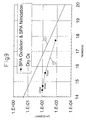
- Fig. 10 shows results of SIMS analysis of an oxide film which has been subjected to SPA-nitridation.
- nitridation was conducted on the underlying oxide film 15A for 8 seconds and 25 seconds, respectively.
- high-density nitrogen atoms are incorporated in the surface region, and it is possible to conduct nitriding while avoiding the deterioration of device characteristics due to the mixing of nitrogen atoms into the interface.
- the extent or range to which the production process according to the present invention is applicable is not particularly limited.
- the extremely thin high-quality oxide film and/or oxynitride film which can be formed by the present invention may particularly preferably be utilized as an insulator constituting a semiconductor device (particularly, gate insulator of an MOS semiconductor structure).
- the present invention can easily produce an MOS semiconductor structure having a preferred characteristic as follows.
- the characteristic of the oxide film and/or oxynitride film which has been formed by the present invention is evaluated, for example, instead of the evaluation of the physical property of the above-mentioned oxide film and/or oxynitride film per se, it is possible that a standard MOS semiconductor structure as described in a paper (OYO BUTURI (Applied Physics), Vol. 69, No. 9, pp. 1049-1059 (2000)) is formed, and the characteristic of the resultant MOS is evaluated. This is because, in such a standard MOS structure, the characteristic of the oxide film and/or oxynitride film constituting the structure has a strong influence on the resultant MOS characteristic.
- the reference numeral 1 denotes a silicon substrate
- the reference numeral 11 denotes a field oxide film
- the reference numeral 2 denotes a gate insulator
- the reference numeral 13 denotes a gate electrode in Fig. 1A.
- the production process according to the present invention can form an extremely thin and high-quality gate insulator 2.
- the gate insulator 2 comprises or consisting of a high-quality insulating film which has been formed at the interface thereof with the silicon substrate 1, as shown in Fig. 1B.
- the gate insulator 2 comprises an oxide film 2 having a thickness of about 2.5 nm.
- the high-quality oxide film 2 may preferably comprise a silicon oxide film (hereinafter, referred to as "SiO 2 film”) which has been produced by a method wherein a substrate to be processed comprising Si as a main component is irradiated with microwave via a plane antenna member having a plurality of .slits in the presence of a process gas comprising O 2 and an inert gas, to thereby generate plasma; and the SiO 2 film is formed on the surface of the above-mentioned substrate to be processed, by using the thus generated plasma.
- SiO 2 film silicon oxide film
- a gate electrode 13 comprising Si as a main component (poly-silicon or amorphous-silicon) is formed.
- Fig. 2 is schematic view (schematic plan view) showing an example of the total arrangement of a semiconductor manufacturing equipment 30 for conducting the process for producing electronic device material according to the present invention.
- a transportation chamber 31 for transporting a wafer W (Fig. 3).
- plasma processing units 32 and 33 for conducting various treatments on the wafer there are disposed: plasma processing units 32 and 33 for conducting various treatments on the wafer, two load lock units 34 and 35 for conducting the communication/cutoff between the respective processing chambers, a heating unit 36 for operating various heating treatments, and a heating reaction furnace 47 for conducting various heating treatments on the wafer.
- These units are disposed so as to surround the transportation chamber 31.
- a preliminary cooling unit 45 and a cooling unit 46 for conducting various kinds of preliminary cooling and cooling treatments are disposed.
- transportation arms 37 and 38 are disposed, so as to transport the wafer W (Fig. 3) between the above-mentioned respective units 32-36.
- loader arms 41 and 42 are disposed on the foreground side of the load lock units 34 and 35 in this figure. These loader arms 41 and 42 can put wafer W in and out with respect to four cassettes 44 which are set on the cassette stage 43, which is disposed on the foreground side of the loader arms 41 and 42.
- an SiO 2 film is formed in the plasma processing unit 32, and the SiO 2 film is surface-nitrided in the plasma processing unit 33.
- the formation of an SiO 2 film and the surface-nitriding of the SiO 2 film are conducted in parallel, in the plasma processing units 32 and 33.
- an SiO 2 film is formed in another apparatus, and the SiO 2 film is surface-nitrided in parallel, in the plasma processing units 32 and 33.
- Fig. 3 is a schematic sectional view in the vertical direction showing a plasma processing unit 32 (or 33) which is usable in the film formation of the gate insulator 2.
- reference numeral 50 denotes a vacuum container made of, e.g., aluminum.
- an opening portion 51 is formed so that the opening portion 51 is larger than a substrate (for example, wafer W).
- a top plate 54 in a flat cylindrical shape made of a dielectric such as quartz and aluminum nitride is provided so as to cover the opening portion 51.
- gas feed pipes 72 are disposed in the 16 positions, which are arranged along the circumferential direction so as to provide equal intervals therebetween.
- a process gas comprising at least one kind of gas selected from O 2 , inert gases, N 2 , H 2 , etc., can be supplied into the plasma region P in the vacuum container 50 from the gas feed pipes 72 evenly and uniformly.
- a radio-frequency power source On the outside of the top plate 54, there is provided a radio-frequency power source, via a plane antenna member having a plurality of slits, which comprises e.g., a slit plane antenna (SPA) made from a copper plate, for example.
- a waveguide 63 is disposed on the top plate 54 by the medium of the SPA 60, and the waveguide 63 is connected to a microwave power supply 61 for generating microwave of 2.45GHz, for example.
- the waveguide 63 comprises a combination of: a flat circular waveguide 63A, of which lower end is connected to the SPA 60; a circular waveguide 63B, one end of which is connected to the upper surface side of the circular waveguide 63A; a coaxial waveguide converter 63C connected to the upper surface side of the circular waveguide 63B; and a rectangular waveguide 63D, one end of which is connected to the side surface of the coaxial waveguide converter 63C so as to provide a right angle therebetween, and the other end of which is connected to the microwave power supply 61.
- a frequency region including UHF and microwave is referred to as radio-frequency (or high-frequency) region.
- the radio-frequency power supplied from the radio-frequency power source may preferably have a frequency of not smaller than 300 MHz and not larger than 2500 MHz, which may include UHF having a frequency of not smaller than 300 MHz and microwave having a frequency of not smaller than 1 GHz.
- the plasma generated by the radio-frequency power is referred to as "radio-frequency plasma".
- an axial portion 62 of an electroconductive material is coaxially provided, so that one end of the axial portion 62 is connected to the central (or nearly central) portion of the SPA 60 upper surface, and the other end of the axial portion 62 is connected to the upper surface of the circular waveguide 63B, whereby the circular waveguide 63B constitutes a coaxial structure.
- the circular waveguide 63B is constituted so as to function as a coaxial waveguide.
- a stage 52 for carrying the wafer W is provided so that the stage 52 is disposed opposite to the top plate 54.
- the stage 52 contains a temperature control unit (not shown) disposed therein, so that the stage can function as a hot plate.
- one end of an exhaust pipe 53 is connected to the bottom portion of the vacuum container 50, and the other end of the exhaust pipe 53 is connected to a vacuum pump 55.
- Fig. 4 is a schematic plan view showing an example of SPA 60 which is usable in an apparatus for producing an electronic device material according to the present invention.
- each slot 60a is a substantially square penetration-type groove.
- the adjacent slots are disposed perpendicularly to each other and arranged so as to form a shape of alphabetical "T"-type character.
- the length and the interval of the slot 60a arrangement are determined in accordance with the wavelength of the microwave supplied from the microwave power supply unit 61.
- Fig. 5 is schematic sectional view in the vertical direction showing an example of the heating reaction furnace 47 which is usable in an apparatus for producing an electronic device material according to the present invention.
- a processing chamber 82 of the heating reaction furnace 47 chamber is formed into an air-tight structure by using aluminum, for example.
- a heating mechanism and a cooling mechanism are provided in the processing chamber 82, although these mechanisms are not shown in Fig. 5.
- a gas introduction pipe 83 for introducing a gas into the processing chamber 82 is connected to the upper central portion of the processing chamber 82, the inside of the processing chamber 82 communicates with the inside of the gas introduction pipe 83.
- the gas introduction pipe 83 is connected to a gas supply source 84.
- a gas is supplied from the gas supply source 84 into the gas introduction pipe 83, and the gas is introduced into the processing chamber 82 through the gas introduction pipe 83.
- the gas in this case, it is possible to use one of various gases such as raw material for forming a gate electrode (electrode-forming gas) such as silane, for example.
- an inert gas as a carrier gas.
- a gas exhaust pipe 85 for exhausting the gas in the processing chamber 82 is connected to the lower portion of the processing chamber 82, and the gas exhaust pipe 85 is connected to exhaust means (not shown) such as vacuum pump. On the basis of the exhaust means, the gas in the processing chamber 82 is exhausted through the gas exhaust pipe 85, and the processing chamber 82 is maintained at a desired pressure.
- a stage 87 for carrying wafer W is provided in the lower portion of the processing chamber 82.
- the wafer W is carried on the stage 87 by means of an electrostatic chuck (not shown) having a diameter which is substantially the same as that of the wafer W.
- the stage 87 contains a heat source means (not shown) disposed therein, to thereby constitute a structure wherein the surface of the wafer W to be processed which is carried on the stage 87 can be adjusted to a desired temperature.
- the stage 87 has a mechanism which is capable of rotating the wafer W carried on the stage 87, as desired.
- an opening portion 82a for putting the wafer W in and out with respect to the processing chamber 82 is provided on the surface of the right side of the processing chamber 82 in this figure.
- the opening portion 82a can be opened and closed by moving a gate valve 98 vertically (up and down direction) in this figure.
- a transportation arm (not shown) for transporting the wafer is provided adjacent to the right side of the gate valve 98.
- the wafer W can be carried on the stage 87, and the wafer W after the processing thereof is transported from the processing chamber 82, as the transportation arm enters the processing chamber 82 and goes out therefrom through the medium of the opening portion 82a.
- a shower head 88 as a shower member is provided above the stage 87.
- the shower head 88 is constituted so as to define the space between the stage 87 and the gas introduction pipe 83, and the shower head 88 is formed from aluminum, for example.
- the shower head 88 is formed so that the gas exit 83a of the gas introduction pipe 83 is positioned at the upper central portion of the shower head 88.
- the gas is introduced into the processing chamber 82 through gas feeding holes 89 provided in the lower portion of the shower head 88.
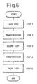
- Fig. 6 is a schematic production process flowchart showing an example of the flow of the respective steps constituting the production process according to the present invention.
- a field oxide film 11 (Fig. 1A) is formed on the surface of a wafer W.
- a gate valve (not shown) provided at the side wall of the vacuum container 50 in the plasma processing unit 32 (Fig. 2) is opened, and the above-mentioned wafer W comprising the silicon substrate 1, and the field oxide film 11 formed on the surface of the silicon substrate 1 is placed on the stage 52 (Fig. 3) by means of transportation arms 37 and 38.
- microwave e.g., of 1.80 GHz and 2200 W
- the microwave is generated by the microwave power supply 61, and the microwave is guided by the waveguide so that the microwave is introduced into the vacuum container 50 via the SPA 60 and the top plate 54, whereby radio-frequency plasma is generated in the plasma region P of an upper portion in the vacuum container 50.
- the microwave is transmitted in the rectangular waveguide 63D in a rectangular mode, and is converted from the rectangular mode into a circular mode by the coaxial waveguide converter 63C.
- the microwave is then transmitted in the cylindrical coaxial waveguide 63B in the circular mode, and transmitted in the circular waveguide 63A in the expanded state, and is emitted from the slots 60a of the SPA 60, and penetrates the plate 54 and is introduced into the vacuum container 50.
- microwave is used, and accordingly high-density plasma can be generated.
- the microwave is emitted from a large number of slots 60a of the SPA 60, and accordingly the plasma is caused to have a high plasma density.
- the first step formation of oxide film
- a process gas for an oxide film formation comprising an inert gas such as krypton and argon, and O 2 gas at flow rates of 1000 sccm, and 20 sccm respectively.
- the introduced process gas is activated (converted into plasma) by plasma flux which has been generated in the plasma processing unit 32, and on the basis of the thus generated plasma, as shown in the schematic sectional view of Fig. 7A, the surface of the silicon substrate 1 is oxidized, to thereby form an oxide film (SiO 2 film) 2.
- the oxidation step is conducted for 40 seconds, for example, so that a gate oxide film or underlying oxide film form (underlying SiO 2 film) for forming a gate oxynitride film having a thickness of 2.5 nm can be formed.
- the gate valve (not shown) is opened, and the transportation arms 37 and 38 (Fig. 2) are caused to enter the vacuum container 50, so as to receive the wafer W on the stage 52.
- the transportation arms 37 and 38 take out the wafer W from the plasma processing unit 32, and then set the wafer W in the stage in the adjacent plasma processing unit 33 (step 2).
- the wafer W is surface-nitrided in the plasma processing unit 33, and a nitride-containing layer 2a (Fig. 7 B) is formed on a surface portion of the underlying oxide (underlying SiO 2 ) film 2 which has been formed in advance.
- argon gas and N 2 gas are introduced into the container 50 from the gas introduction pipe at flow rates of 1000 sccm and 20 sccm, respectively, in a state where the wafer temperature is 400 °C, for example, and the process pressure is 66.7 Pa (500 mTorr), for example, in the vacuum container 50.
- microwave e.g., of 2 W/cm 2 is generated from the microwave power supply 61, and the microwave is guided by the waveguide so that the microwave is introduced into the vacuum container 50 via the SPA 60 and the top plate 54, whereby radio-frequency plasma is generated in the plasma region P of an upper portion in the vacuum container 50.
- the introduced gas is converted into plasma, and nitrogen radicals are formed. These nitrogen radicals are reacted on the SiO 2 film disposed on the wafer W surface, to thereby nitride the SiO 2 film surface in a relatively short period.
- a nitrogen-containing layer 2a is formed on the surface of the underlying oxide film (underlying SiO 2 film) 2 on the wafer W.
- SiON film a gate oxynitride film having a thickness of about 2 nm in terms of the equivalent film thickness by conducting this nitriding treatment for 20 seconds, for example.
- a gate electrode 13 (Fig. 1A) is formed on the SiO 2 film on the wafer W, or on the SiON film which has been formed by nitriding the underlying SiO 2 film on the wafer W.
- the wafer W on which the gate oxide film or gate oxynitride film has been formed is taken out from each of the plasma processing unit 32 or 33, so as to once accommodate the wafer W in the transportation chamber 31 (Fig. 2) side, and then the wafer W is accommodated into the heating reaction furnace 47 (step 4).
- the heating reaction furnace 47 the wafer W is heated under a predetermined processing condition to thereby form a predetermined gate electrode 13 on the gate oxide film or gate oxynitride film.
- the step is conducted under conditions such that SiH 4 is used as the process gas (electrode-forming gas), the pressure is 20.0-33.3 Pa (150-250 mTorr), and the temperature is 570-630 °C.
- the step is conducted under conditions such that SiH 4 is used as the process gas (electrode-forming gas), the pressure is 20.0-66.7 Pa (150-500 mTorr), and the temperature is 520-570 °C.
- the wafer W comprising Si as a main component is irradiated with microwave in the presence of a process gas via a plane antenna member (SPA) having a plurality of slits, so as to form plasma comprising oxygen (O 2 ) and an inert gas, to thereby form the oxide film on the surface of the above-mentioned substrate to be processed.
- SPA plane antenna member
- the quality of the oxide film in the first process is high as shown in the graph of Fig. 8.
- the Fig. 8 shows the leakage characteristic of an MOS-type semiconductor structure which has been formed on a silicon wafer W by the process for producing the electronic device material regarding the above-mentioned embodiment.
- the ordinate is the value of the leakage current
- the abscissa is the electric film thickness (equivalent film thickness).
- the graph (1) shown by a solid line denotes the leakage characteristic of the thermal oxide film (DryOx) which has been formed by the conventional thermal oxidation process (Dry thermal oxidation process), for the purpose of comparison
- the graph (2) denotes the leakage characteristic of the oxide film (SPAOx) which has been obtained by the plasma processing by use of SPA in the presence of O 2 and argon as an inert gas.
- the value of the leakage of the oxide film (2) which has been formed by the process for producing electronic device material according to the present invention is low, as compared with the leakage characteristic (1) of the thermal oxidation film which has been formed by the conventional thermal oxidation process. Therefore, a low power consumption is realized and good device characteristic can be obtained by using the oxide film formed by the present invention.
- a high-quality oxide film (gate oxide film, for example) having a low interface state could be obtained by a process for producing electronic device material according to the present invention.
- the reason for the improvement in the film quality of the oxide film which has been formed by the above-mentioned process may be presumed as follows.
- the plasma which has been formed by irradiating a process gas with microwave by use of an SPA is one having a relatively low electron temperature. Therefore, the bias between the plasma and the surface of the substrate to be processed can be suppressed to a relatively low value, and the plasma damage is light. Therefore, it is considered that an SiO 2 film having a good interfacial quality can be formed as shown in Fig. 8.
- the oxynitride film which has been obtained by the surface nitriding in the above-mentioned second step has an excellent quality. According to the present inventor's knowledge and investigations, the reason for such a film quality may be presumed as follow.
- the nitrogen radicals which have been generated on the oxide film surface on the basis of the above-mentioned SPA have a high density, and therefore they can introduce nitrogen atoms in a surface portion of the oxide film, to thereby mix the nitrogen radicals therein at a concentration of several percents.
- high-density radicals can be generated even at a low temperature (around room temperature), whereby the deterioration in the device characteristic due to heat (represented by those due to the diffusion of a dopant) can be suppressed.
- the nitrogen atoms in the film are incorporated in the surface portion of the oxide film, and accordingly, they can improve the dielectric constant and further can exhibit a certain performance (such as effect of preventing the penetration of boron atoms), without deteriorating the interfacial quality.
- the gate electrode is formed by the heat treatment under a specific condition in the above-mentioned third step, the resultant MOS-type semiconductor structure has an excellent characteristic. According to the present inventors' knowledge and investigations, the reason therefor may be presumed as follows.
- an extremely thin high-quality gate insulator can be formed.
- the high-quality gate insulator gate oxide film and/or gate oxynitride film
- the gate electrode for example, SiGe, amorphous-silicon, poly-silicon by CVD
- the exposure of the gate insulator to the atmosphere can be avoided during a period between the formation of the gate oxide film or gate oxynitride film, and the formation of the gate electrode, to thereby further improve the yield and device characteristic.
- an underlying SiO 2 film having a film thickness of 1.8 nm was formed on an N-type silicon substrate which had been subjected to element-isolation formation, by means of an appratus shown in Fig. 2 by using SPA plasma in the process unit 32.
- the resultant total thickness was 1.8 nm in terms of oxide film thickness (equivalent film thickness).
- the nitridation time was changed so as to provide values of 10 seconds, 20 seconds, and 40 seconds. A throughput of 25 sheets/hour per one chamber was achieved, and it was confirmed that such a throughput was sufficiently applicable to an industrial use.
- the equivalent film thickness was determined from the resultant C-V characteristic.
- the equivalent film thickness was decreased to about 1.4 nm, and the uniformity in the film thickness was 4 % in terms of three-sigma, whereby good results were provided.
- the gate leakage current characteristic was measured.
- the ordinate is the leakage current characteristic
- the abscissa is the electric film thickness (equivalent film thickness).
- the graph (1) shown by a straight line denotes the leakage characteristic of a normal (or standard) thermal oxide film
- the graph (2) shown by points denotes the leakage characteristic of a film which had been obtained by nitridation after the SPA oxidation.
- a reduction in the equivalent film thickness was observed along with an increase in the nitridation period.
- the leakage current was decreased by a factor of about one digit, at most, as compared with that of the normal thermal oxide film.
- the process for producing electronic device material according to the present invention could provide a high-performance MOS-type semiconductor structure having a good electric characteristic at a throughput which is sufficiently applicable to an industrial use.
- a substrate to be processed comprising Si as a main component is irradiated in the presence of a process gas with microwave via a plane antenna member having a plurality of slits (so-called SPA antenna), whereby plasma is directly supplied to the silicon-containing substrate to form an oxide film (SiO 2 film).
- SPA antenna plane antenna member having a plurality of slits
- the present invention can preferably control the characteristic of the interface (or boundary) between the silicon-containing substrate and the oxide film (SiO 2 film) to be foomed thereon.
- an underlying oxide film (SiO 2 film) is subjected to surface-nitriding by using a so-called SPA antenna, to thereby form a high-quality oxynitride film (SiON film).
- a gate electrode for example, gate electrode comprising poly-silicon or amorphous-silicon or SiGe
- an semiconductor structure for example, MOS-type semiconductor structure
Landscapes
- Chemical & Material Sciences (AREA)
- Chemical Kinetics & Catalysis (AREA)
- Engineering & Computer Science (AREA)
- Materials Engineering (AREA)
- Mechanical Engineering (AREA)
- Metallurgy (AREA)
- Organic Chemistry (AREA)
- General Chemical & Material Sciences (AREA)
- Formation Of Insulating Films (AREA)
- Insulated Gate Type Field-Effect Transistor (AREA)
Abstract
Description
a gas comprising N2 at a flow rate of 4-200 sccm, krypton, argon or helium at a flow rate of 500-2000 sccm, and H2 at a flow rate of 2-30 sccm.
the surface of the above-mentioned underlying SiO2 film is nitrided by using plasma based on microwave irradiation via a plane antenna member having a plurality of slits, in the presence of a process gas comprising at least an inert gas and N2; and
the substrate to be processed having the above-mentioned SiO2 film or surface-nitrided underlying SiO2 film (SiON film) is heated in the presence of a layer-forming gas, to thereby an electrode layer (for example, electrode layer comprising poly-silicon or amorphous-silicon or SiGe) on the above-mentioned SiO2 film or SiON film.
Claims (26)
- A process for producing electronic device material, wherein an oxide film (SiO2 film) is formed on the surface of a substrate to be processed comprising Si as a main component in the presence of a process gas comprising at least O2 and an inert gas, by using plasma based on microwave irradiation via a plane antenna member having a plurality of slits.
- A process for producing electronic device material according to claim 1, wherein the electronic device is a semiconductor device.
- A process for producing electronic device material according to claim 2, wherein the oxide film is a gate oxide film (SiO2 film) or an underlying oxide film (underlying SiO2 film) for a gate oxynitride film.
- A process for producing electronic device material according to any one of claims 1-3, wherein the oxide film has a thickness of 2.5 nm or less.
- A process for producing electronic device material according to any one of claims 1-4, wherein the inert gas is at least one selected from krypton, argon and helium.
- A process for producing electronic device material according to any one of claims 1-5, wherein the process gas comprises O2 at a flow rate of 5-500 sccm, and krypton, argon or helium at a flow rate of 500-3000 sccm.
- A process for producing electronic device material according to any one of claims 1-6, wherein the SiO2 film is formed at a temperature of room temperature to 700 °C.
- A process for producing electronic device material according to any one of claims 1-4, wherein the SiO2 film is formed at a pressure of 20-5000 mTorr.
- A process for producing electronic device material according to any one of claims 1-8, wherein the plasma is generated by an output of 0.5-5 W/cm2.
- A process for producing electronic device material, comprising:a step of forming an underlying oxide film (SiO2 film) in the presence of a process gas comprising at least O2 and an inert gas, on the surface of a substrate to be processed comprising Si as a main component, by using plasma based on microwave irradiation via a plane antenna member having a plurality of slits; anda step of nitriding the surface portion of the underlying SiO2 film, in the presence of a process gas comprising at least N2 and an inert gas, by using plasma based on microwave irradiation via a plane antenna member having a plurality of slits.
- A process for producing electronic device material according to claim 10, wherein the electronic device is a semiconductor device.
- A process for producing electronic device material according to claim 10 or 11, wherein the process gas further comprises H2.
- A process for producing electronic device material according to any one of claims 10-12, wherein the oxide film is a gate oxide film (SiO2 film) or an underlying oxide film (underlying SiO2 film) for a gate oxynitride film.
- A process for producing electronic device material according to any one of claims 10-13, wherein the oxide film has a thickness of 2.5 nm or less.
- A process for producing electronic device material according to any one of claims 10-14, wherein the inert gas is at least one selected from krypton, argon and helium.
- A process for producing electronic device material according to any one of claims 10-15, wherein the process gas comprises N2 at a flow rate of 2-500 sccm, and krypton, argon or helium at a flow rate of 200-2000 sccm; or comprises N2 at a flow rate of 2-500 sccm, and krypton, argon or helium at a flow rate of 200-2000 sccm, and H at a flow rate of 1-100 sccm.
- A process for producing electronic device material according to any.one of claims 10-16, wherein the underlying SiO2 film is nitrided at a temperature of room temperature to 700 °C.
- A process for producing electronic device material according to any one of claims 10-17, wherein the underlying SiO2 film is nitrided at a pressure of 10-3000 mTorr.
- A process for producing electronic device material according to any one of claims 10-18, wherein the nitriding plasma is generated by an output of 0.5-4 W/cm2.
- A process for producing electronic device material, comprising:a step of forming an underlying oxide film (SiO2 film) in the presence of a process gas comprising at least O2 and an inert gas, on the surface of a substrate to be processed comprising Si as a main component, by using plasma based on microwave irradiation via a plane antenna member having a plurality of slits;a step of nitriding the surface portion of the underlying SiO2 film, in the presence of a process gas comprising at least N2 and an inert gas, by using plasma based on microwave irradiation via a plane antenna member having a plurality of slits; anda step of forming an electrode layer on the SiO2 film or the surface-nitrided underlying SiO2 film (SiON film) by heating the substrate to be processed having the SiO2 film or SiON film in the presence of a layer-forming gas.
- A process for producing electronic device material according to claim 20, wherein the electrode layer comprises poly-silicon or amorphous-silicon or SiGe.
- A process for producing electronic device material according to claim 20 or 21, wherein the electronic device is a semiconductor device.
- A process for producing electronic device material according to any one of claims 20-22, wherein the electrode layer is a gate electrode.
- A process for producing electronic device material according to any one of claims 20-23, wherein the layer-forming gas is SiH4, the pressure is 20.0-40 Pa (150-300 mTorr), and the temperature is 570-650 °C, and the gate electrode to be formed comprises poly-silicon.
- A process for producing electronic device material according to any one of claims 20-23, wherein the layer-forming gas is SiH4, the pressure is 20.0-66.7 Pa (150-500 mTorr), the temperature is 520-570 °C, and the gate electrode to be formed comprises amorphous-silicon.
- A process for producing electronic device material according to any one of claims 20-23, wherein the layer-forming gas is a mixed gas of GeH4/SiH4 = 10/90-60/40 %, the pressure is 20-60 Pa, the temperature is 460-560 °C, he gate electrode to be formed comprises SiGe.
Applications Claiming Priority (3)
| Application Number | Priority Date | Filing Date | Title |
|---|---|---|---|
| JP2001012917 | 2001-01-22 | ||
| JP2001012917 | 2001-01-22 | ||
| PCT/JP2002/000439 WO2002058130A1 (en) | 2001-01-22 | 2002-01-22 | Method for producing material of electronic device |
Publications (2)
| Publication Number | Publication Date |
|---|---|
| EP1361605A1 true EP1361605A1 (en) | 2003-11-12 |
| EP1361605A4 EP1361605A4 (en) | 2006-02-15 |
Family
ID=18879853
Family Applications (1)
| Application Number | Title | Priority Date | Filing Date |
|---|---|---|---|
| EP02715873A Withdrawn EP1361605A4 (en) | 2001-01-22 | 2002-01-22 | PRODUCTION PROCESS |
Country Status (6)
| Country | Link |
|---|---|
| US (3) | US20040142577A1 (en) |
| EP (1) | EP1361605A4 (en) |
| JP (3) | JP3916565B2 (en) |
| KR (4) | KR100994387B1 (en) |
| CN (2) | CN100477113C (en) |
| WO (1) | WO2002058130A1 (en) |
Cited By (12)
| Publication number | Priority date | Publication date | Assignee | Title |
|---|---|---|---|---|
| WO2003096403A1 (en) | 2002-05-13 | 2003-11-20 | Tokyo Electron Limited | Method of treating substrate |
| EP1361606A4 (en) * | 2001-01-25 | 2005-06-29 | Tokyo Electron Ltd | METHOD FOR MANUFACTURING ELECTRONIC DEVICE MATERIAL |
| WO2006107416A3 (en) * | 2005-03-30 | 2007-11-15 | Tokyo Electron Ltd | Method and system for forming an oxynitride layer by performing oxidation and nitridation concurrently |
| WO2007053269A3 (en) * | 2005-10-31 | 2007-12-21 | Tokyo Electron Ltd | Method and system for forming a nitrided germanium-containing layer using plasma processing |
| EP1670049A4 (en) * | 2003-09-17 | 2008-06-04 | Tokyo Electron Ltd | PRODUCTION OF INSULATING FILM WITH LOW DIELECTRIC CONSTANT |
| US7501352B2 (en) | 2005-03-30 | 2009-03-10 | Tokyo Electron, Ltd. | Method and system for forming an oxynitride layer |
| US7517812B2 (en) | 2005-10-31 | 2009-04-14 | Tokyo Electron Limited | Method and system for forming a nitrided germanium-containing layer using plasma processing |
| US7713876B2 (en) | 2005-09-28 | 2010-05-11 | Tokyo Electron Limited | Method for integrating a ruthenium layer with bulk copper in copper metallization |
| CN101313393B (en) * | 2006-02-28 | 2010-06-09 | 东京毅力科创株式会社 | Plasma oxidation treatment method and semiconductor device manufacturing method |
| DE112010001364T5 (en) | 2009-03-26 | 2012-10-11 | Tokyo Electron Ltd. | A method of forming a high k gate stack with reduced effective oxide thickness |
| US20140346650A1 (en) * | 2009-08-14 | 2014-11-27 | Asm Ip Holding B.V. | Systems and methods for thin-film deposition of metal oxides using excited nitrogen-oxygen species |
| EP2732065B1 (en) * | 2011-07-12 | 2019-02-13 | HQ-Dielectrics GmbH | Method for forming a layer on a substrate at low temperatures |
Families Citing this family (380)
| Publication number | Priority date | Publication date | Assignee | Title |
|---|---|---|---|---|
| CN100477113C (en) * | 2001-01-22 | 2009-04-08 | 东京毅力科创株式会社 | Method for manufacturing electronic device material |
| JP4256340B2 (en) * | 2002-05-16 | 2009-04-22 | 東京エレクトロン株式会社 | Substrate processing method |
| US7122454B2 (en) * | 2002-06-12 | 2006-10-17 | Applied Materials, Inc. | Method for improving nitrogen profile in plasma nitrided gate dielectric layers |
| US7067439B2 (en) | 2002-06-14 | 2006-06-27 | Applied Materials, Inc. | ALD metal oxide deposition process using direct oxidation |
| TWI235433B (en) * | 2002-07-17 | 2005-07-01 | Tokyo Electron Ltd | Oxide film forming method, oxide film forming apparatus and electronic device material |
| JP2004175927A (en) * | 2002-11-27 | 2004-06-24 | Canon Inc | Surface modification method |
| WO2004070816A1 (en) * | 2003-02-06 | 2004-08-19 | Tokyo Electron Limited | Plasma processing method, semiconductor substrate and plasma processing system |
| TWI229368B (en) * | 2003-02-13 | 2005-03-11 | Tokyo Electron Ltd | Manufacturing method for semiconductor device and semiconductor manufacturing device |
| JP2004266075A (en) * | 2003-02-28 | 2004-09-24 | Tokyo Electron Ltd | Substrate processing method |
| TW200511430A (en) * | 2003-05-29 | 2005-03-16 | Tokyo Electron Ltd | Plasma processing apparatus and plasma processing method |
| US20040262701A1 (en) * | 2003-06-24 | 2004-12-30 | Texas Instruments Incorporated | Nitridation process for independent control of device gate leakage and drive current |
| US7291568B2 (en) * | 2003-08-26 | 2007-11-06 | International Business Machines Corporation | Method for fabricating a nitrided silicon-oxide gate dielectric |
| JP4555143B2 (en) * | 2004-05-11 | 2010-09-29 | 東京エレクトロン株式会社 | Substrate processing method |
| US8119210B2 (en) | 2004-05-21 | 2012-02-21 | Applied Materials, Inc. | Formation of a silicon oxynitride layer on a high-k dielectric material |
| JPWO2006046634A1 (en) | 2004-10-28 | 2008-05-22 | 東京エレクトロン株式会社 | Method for forming gate insulating film, semiconductor device, and computer recording medium |
| JP4718189B2 (en) | 2005-01-07 | 2011-07-06 | 東京エレクトロン株式会社 | Plasma processing method |
| CN101053083B (en) * | 2005-02-01 | 2011-01-12 | 东京毅力科创株式会社 | Semiconductor device manufacturing method and plasma oxidation method |
| US8974868B2 (en) * | 2005-03-21 | 2015-03-10 | Tokyo Electron Limited | Post deposition plasma cleaning system and method |
| US20060228898A1 (en) * | 2005-03-30 | 2006-10-12 | Cory Wajda | Method and system for forming a high-k dielectric layer |
| JP2006310736A (en) * | 2005-03-30 | 2006-11-09 | Tokyo Electron Ltd | Method for manufacturing gate insulating film and method for manufacturing semiconductor device |
| KR101028625B1 (en) * | 2005-03-31 | 2011-04-12 | 도쿄엘렉트론가부시키가이샤 | Nitriding treatment method of substrate and forming method of insulating film |
| KR101123442B1 (en) * | 2005-04-15 | 2012-03-23 | 도쿄엘렉트론가부시키가이샤 | Method for manufacturing semiconductor device manufacturing method, semiconductor device, method for plasma nitriding treatment method, control program and computer storage medium |
| US8318554B2 (en) * | 2005-04-28 | 2012-11-27 | Semiconductor Energy Laboratory Co., Ltd. | Method of forming gate insulating film for thin film transistors using plasma oxidation |
| WO2006132262A1 (en) * | 2005-06-08 | 2006-12-14 | Tohoku University | Plasma nitriding method, method for manufacturing semiconductor device and plasma processing apparatus |
| JP2007073395A (en) | 2005-09-08 | 2007-03-22 | Tokyo Electron Ltd | Magnetron control method, magnetron life determination method, microwave generator, magnetron life determination device, processing device, and storage medium |
| US20070065593A1 (en) * | 2005-09-21 | 2007-03-22 | Cory Wajda | Multi-source method and system for forming an oxide layer |
| US20070066084A1 (en) * | 2005-09-21 | 2007-03-22 | Cory Wajda | Method and system for forming a layer with controllable spstial variation |
| KR100649874B1 (en) * | 2005-12-29 | 2006-11-27 | 동부일렉트로닉스 주식회사 | Transistor manufacturing method using SOH wafer |
| KR100745370B1 (en) * | 2006-01-20 | 2007-08-02 | 삼성전자주식회사 | Method of manufacturing insulating film of semiconductor device |
| US7837838B2 (en) | 2006-03-09 | 2010-11-23 | Applied Materials, Inc. | Method of fabricating a high dielectric constant transistor gate using a low energy plasma apparatus |
| US7645710B2 (en) | 2006-03-09 | 2010-01-12 | Applied Materials, Inc. | Method and apparatus for fabricating a high dielectric constant transistor gate using a low energy plasma system |
| US7678710B2 (en) | 2006-03-09 | 2010-03-16 | Applied Materials, Inc. | Method and apparatus for fabricating a high dielectric constant transistor gate using a low energy plasma system |
| US8580034B2 (en) * | 2006-03-31 | 2013-11-12 | Tokyo Electron Limited | Low-temperature dielectric formation for devices with strained germanium-containing channels |
| WO2008039845A2 (en) | 2006-09-26 | 2008-04-03 | Applied Materials, Inc. | Fluorine plasma treatment of high-k gate stack for defect passivation |
| US20100029093A1 (en) * | 2006-09-29 | 2010-02-04 | Tokyo Electron Limited | Plasma oxidizing method, plasma processing apparatus, and storage medium |
| JP5231232B2 (en) * | 2006-09-29 | 2013-07-10 | 東京エレクトロン株式会社 | Plasma oxidation processing method, plasma processing apparatus, and storage medium |
| WO2008041599A1 (en) * | 2006-09-29 | 2008-04-10 | Tokyo Electron Limited | Plasma oxidizing method, storage medium, and plasma processing apparatus |
| JP4864661B2 (en) * | 2006-11-22 | 2012-02-01 | 東京エレクトロン株式会社 | Solar cell manufacturing method and solar cell manufacturing apparatus |
| KR100850138B1 (en) * | 2006-12-26 | 2008-08-04 | 동부일렉트로닉스 주식회사 | Gate insulating film and method of forming the semiconductor device |
| US7767579B2 (en) | 2007-12-12 | 2010-08-03 | International Business Machines Corporation | Protection of SiGe during etch and clean operations |
| KR101249611B1 (en) * | 2008-01-24 | 2013-04-01 | 도쿄엘렉트론가부시키가이샤 | Method for forming silicon oxide film, storage medium, and plasma processing apparatus |
| JP4593652B2 (en) * | 2008-06-06 | 2010-12-08 | 東京エレクトロン株式会社 | Microwave plasma processing equipment |
| KR101111962B1 (en) * | 2008-10-24 | 2012-06-12 | 한국기초과학지원연구원 | Apparatus and method for forming nitridation film of using the nitrogen atom beam |
| US9394608B2 (en) | 2009-04-06 | 2016-07-19 | Asm America, Inc. | Semiconductor processing reactor and components thereof |
| TWI529774B (en) * | 2010-03-31 | 2016-04-11 | 東京威力科創股份有限公司 | Plasma Nitriding Process and Plasma Processing Device |
| US8753456B2 (en) * | 2010-06-25 | 2014-06-17 | Apple Inc. | Selective nitriding on a 3D surface |
| JP2011204687A (en) * | 2011-05-20 | 2011-10-13 | Tokyo Electron Ltd | Lifetime determination method for magnetron, lifetime determination device for magnetron, and processing apparatus |
| US9312155B2 (en) | 2011-06-06 | 2016-04-12 | Asm Japan K.K. | High-throughput semiconductor-processing apparatus equipped with multiple dual-chamber modules |
| US10854498B2 (en) | 2011-07-15 | 2020-12-01 | Asm Ip Holding B.V. | Wafer-supporting device and method for producing same |
| US20130023129A1 (en) | 2011-07-20 | 2013-01-24 | Asm America, Inc. | Pressure transmitter for a semiconductor processing environment |
| US9017481B1 (en) | 2011-10-28 | 2015-04-28 | Asm America, Inc. | Process feed management for semiconductor substrate processing |
| US10714315B2 (en) | 2012-10-12 | 2020-07-14 | Asm Ip Holdings B.V. | Semiconductor reaction chamber showerhead |
| US20160376700A1 (en) | 2013-02-01 | 2016-12-29 | Asm Ip Holding B.V. | System for treatment of deposition reactor |
| US10683571B2 (en) | 2014-02-25 | 2020-06-16 | Asm Ip Holding B.V. | Gas supply manifold and method of supplying gases to chamber using same |
| US10167557B2 (en) | 2014-03-18 | 2019-01-01 | Asm Ip Holding B.V. | Gas distribution system, reactor including the system, and methods of using the same |
| US11015245B2 (en) | 2014-03-19 | 2021-05-25 | Asm Ip Holding B.V. | Gas-phase reactor and system having exhaust plenum and components thereof |
| US10858737B2 (en) | 2014-07-28 | 2020-12-08 | Asm Ip Holding B.V. | Showerhead assembly and components thereof |
| US9890456B2 (en) | 2014-08-21 | 2018-02-13 | Asm Ip Holding B.V. | Method and system for in situ formation of gas-phase compounds |
| KR102293862B1 (en) | 2014-09-15 | 2021-08-25 | 삼성전자주식회사 | Method for manufacturing of a semiconductor device |
| US9657845B2 (en) | 2014-10-07 | 2017-05-23 | Asm Ip Holding B.V. | Variable conductance gas distribution apparatus and method |
| US10941490B2 (en) | 2014-10-07 | 2021-03-09 | Asm Ip Holding B.V. | Multiple temperature range susceptor, assembly, reactor and system including the susceptor, and methods of using the same |
| US10276355B2 (en) | 2015-03-12 | 2019-04-30 | Asm Ip Holding B.V. | Multi-zone reactor, system including the reactor, and method of using the same |
| US10458018B2 (en) | 2015-06-26 | 2019-10-29 | Asm Ip Holding B.V. | Structures including metal carbide material, devices including the structures, and methods of forming same |
| US10600673B2 (en) | 2015-07-07 | 2020-03-24 | Asm Ip Holding B.V. | Magnetic susceptor to baseplate seal |
| US10211308B2 (en) | 2015-10-21 | 2019-02-19 | Asm Ip Holding B.V. | NbMC layers |
| US11139308B2 (en) | 2015-12-29 | 2021-10-05 | Asm Ip Holding B.V. | Atomic layer deposition of III-V compounds to form V-NAND devices |
| US10529554B2 (en) | 2016-02-19 | 2020-01-07 | Asm Ip Holding B.V. | Method for forming silicon nitride film selectively on sidewalls or flat surfaces of trenches |
| US10343920B2 (en) | 2016-03-18 | 2019-07-09 | Asm Ip Holding B.V. | Aligned carbon nanotubes |
| US10190213B2 (en) | 2016-04-21 | 2019-01-29 | Asm Ip Holding B.V. | Deposition of metal borides |
| US10865475B2 (en) | 2016-04-21 | 2020-12-15 | Asm Ip Holding B.V. | Deposition of metal borides and silicides |
| US10367080B2 (en) | 2016-05-02 | 2019-07-30 | Asm Ip Holding B.V. | Method of forming a germanium oxynitride film |
| US10032628B2 (en) | 2016-05-02 | 2018-07-24 | Asm Ip Holding B.V. | Source/drain performance through conformal solid state doping |
| US11453943B2 (en) | 2016-05-25 | 2022-09-27 | Asm Ip Holding B.V. | Method for forming carbon-containing silicon/metal oxide or nitride film by ALD using silicon precursor and hydrocarbon precursor |
| US10612137B2 (en) | 2016-07-08 | 2020-04-07 | Asm Ip Holdings B.V. | Organic reactants for atomic layer deposition |
| US9859151B1 (en) | 2016-07-08 | 2018-01-02 | Asm Ip Holding B.V. | Selective film deposition method to form air gaps |
| US10714385B2 (en) | 2016-07-19 | 2020-07-14 | Asm Ip Holding B.V. | Selective deposition of tungsten |
| US9887082B1 (en) | 2016-07-28 | 2018-02-06 | Asm Ip Holding B.V. | Method and apparatus for filling a gap |
| US9812320B1 (en) | 2016-07-28 | 2017-11-07 | Asm Ip Holding B.V. | Method and apparatus for filling a gap |
| KR102532607B1 (en) | 2016-07-28 | 2023-05-15 | 에이에스엠 아이피 홀딩 비.브이. | Substrate processing apparatus and method of operating the same |
| US10643826B2 (en) | 2016-10-26 | 2020-05-05 | Asm Ip Holdings B.V. | Methods for thermally calibrating reaction chambers |
| US11532757B2 (en) | 2016-10-27 | 2022-12-20 | Asm Ip Holding B.V. | Deposition of charge trapping layers |
| US10714350B2 (en) | 2016-11-01 | 2020-07-14 | ASM IP Holdings, B.V. | Methods for forming a transition metal niobium nitride film on a substrate by atomic layer deposition and related semiconductor device structures |
| US10229833B2 (en) | 2016-11-01 | 2019-03-12 | Asm Ip Holding B.V. | Methods for forming a transition metal nitride film on a substrate by atomic layer deposition and related semiconductor device structures |
| US10643904B2 (en) | 2016-11-01 | 2020-05-05 | Asm Ip Holdings B.V. | Methods for forming a semiconductor device and related semiconductor device structures |
| US10134757B2 (en) | 2016-11-07 | 2018-11-20 | Asm Ip Holding B.V. | Method of processing a substrate and a device manufactured by using the method |
| KR102546317B1 (en) | 2016-11-15 | 2023-06-21 | 에이에스엠 아이피 홀딩 비.브이. | Gas supply unit and substrate processing apparatus including the same |
| KR102762543B1 (en) | 2016-12-14 | 2025-02-05 | 에이에스엠 아이피 홀딩 비.브이. | Substrate processing apparatus |
| US11581186B2 (en) | 2016-12-15 | 2023-02-14 | Asm Ip Holding B.V. | Sequential infiltration synthesis apparatus |
| US11447861B2 (en) | 2016-12-15 | 2022-09-20 | Asm Ip Holding B.V. | Sequential infiltration synthesis apparatus and a method of forming a patterned structure |
| KR102700194B1 (en) | 2016-12-19 | 2024-08-28 | 에이에스엠 아이피 홀딩 비.브이. | Substrate processing apparatus |
| US10269558B2 (en) | 2016-12-22 | 2019-04-23 | Asm Ip Holding B.V. | Method of forming a structure on a substrate |
| US10867788B2 (en) | 2016-12-28 | 2020-12-15 | Asm Ip Holding B.V. | Method of forming a structure on a substrate |
| US11390950B2 (en) | 2017-01-10 | 2022-07-19 | Asm Ip Holding B.V. | Reactor system and method to reduce residue buildup during a film deposition process |
| US10655221B2 (en) | 2017-02-09 | 2020-05-19 | Asm Ip Holding B.V. | Method for depositing oxide film by thermal ALD and PEALD |
| US10468261B2 (en) | 2017-02-15 | 2019-11-05 | Asm Ip Holding B.V. | Methods for forming a metallic film on a substrate by cyclical deposition and related semiconductor device structures |
| US10529563B2 (en) | 2017-03-29 | 2020-01-07 | Asm Ip Holdings B.V. | Method for forming doped metal oxide films on a substrate by cyclical deposition and related semiconductor device structures |
| USD876504S1 (en) | 2017-04-03 | 2020-02-25 | Asm Ip Holding B.V. | Exhaust flow control ring for semiconductor deposition apparatus |
| KR102457289B1 (en) | 2017-04-25 | 2022-10-21 | 에이에스엠 아이피 홀딩 비.브이. | Method for depositing a thin film and manufacturing a semiconductor device |
| US10892156B2 (en) | 2017-05-08 | 2021-01-12 | Asm Ip Holding B.V. | Methods for forming a silicon nitride film on a substrate and related semiconductor device structures |
| US10770286B2 (en) | 2017-05-08 | 2020-09-08 | Asm Ip Holdings B.V. | Methods for selectively forming a silicon nitride film on a substrate and related semiconductor device structures |
| US12040200B2 (en) | 2017-06-20 | 2024-07-16 | Asm Ip Holding B.V. | Semiconductor processing apparatus and methods for calibrating a semiconductor processing apparatus |
| US11306395B2 (en) | 2017-06-28 | 2022-04-19 | Asm Ip Holding B.V. | Methods for depositing a transition metal nitride film on a substrate by atomic layer deposition and related deposition apparatus |
| US10685834B2 (en) | 2017-07-05 | 2020-06-16 | Asm Ip Holdings B.V. | Methods for forming a silicon germanium tin layer and related semiconductor device structures |
| TWI794238B (en) | 2017-07-13 | 2023-03-01 | 荷蘭商Asm智慧財產控股公司 | Apparatus and method for removal of oxide and carbon from semiconductor films in a single processing chamber |
| KR20190009245A (en) | 2017-07-18 | 2019-01-28 | 에이에스엠 아이피 홀딩 비.브이. | Methods for forming a semiconductor device structure and related semiconductor device structures |
| US10541333B2 (en) | 2017-07-19 | 2020-01-21 | Asm Ip Holding B.V. | Method for depositing a group IV semiconductor and related semiconductor device structures |
| US11374112B2 (en) | 2017-07-19 | 2022-06-28 | Asm Ip Holding B.V. | Method for depositing a group IV semiconductor and related semiconductor device structures |
| US11018002B2 (en) | 2017-07-19 | 2021-05-25 | Asm Ip Holding B.V. | Method for selectively depositing a Group IV semiconductor and related semiconductor device structures |
| US10590535B2 (en) | 2017-07-26 | 2020-03-17 | Asm Ip Holdings B.V. | Chemical treatment, deposition and/or infiltration apparatus and method for using the same |
| TWI815813B (en) | 2017-08-04 | 2023-09-21 | 荷蘭商Asm智慧財產控股公司 | Showerhead assembly for distributing a gas within a reaction chamber |
| US10770336B2 (en) | 2017-08-08 | 2020-09-08 | Asm Ip Holding B.V. | Substrate lift mechanism and reactor including same |
| US10692741B2 (en) | 2017-08-08 | 2020-06-23 | Asm Ip Holdings B.V. | Radiation shield |
| US11139191B2 (en) | 2017-08-09 | 2021-10-05 | Asm Ip Holding B.V. | Storage apparatus for storing cassettes for substrates and processing apparatus equipped therewith |
| US11769682B2 (en) | 2017-08-09 | 2023-09-26 | Asm Ip Holding B.V. | Storage apparatus for storing cassettes for substrates and processing apparatus equipped therewith |
| US10249524B2 (en) | 2017-08-09 | 2019-04-02 | Asm Ip Holding B.V. | Cassette holder assembly for a substrate cassette and holding member for use in such assembly |
| USD900036S1 (en) | 2017-08-24 | 2020-10-27 | Asm Ip Holding B.V. | Heater electrical connector and adapter |
| US11830730B2 (en) | 2017-08-29 | 2023-11-28 | Asm Ip Holding B.V. | Layer forming method and apparatus |
| US11056344B2 (en) | 2017-08-30 | 2021-07-06 | Asm Ip Holding B.V. | Layer forming method |
| US11295980B2 (en) | 2017-08-30 | 2022-04-05 | Asm Ip Holding B.V. | Methods for depositing a molybdenum metal film over a dielectric surface of a substrate by a cyclical deposition process and related semiconductor device structures |
| KR102491945B1 (en) | 2017-08-30 | 2023-01-26 | 에이에스엠 아이피 홀딩 비.브이. | Substrate processing apparatus |
| KR102401446B1 (en) | 2017-08-31 | 2022-05-24 | 에이에스엠 아이피 홀딩 비.브이. | Substrate processing apparatus |
| KR102630301B1 (en) | 2017-09-21 | 2024-01-29 | 에이에스엠 아이피 홀딩 비.브이. | Method of sequential infiltration synthesis treatment of infiltrateable material and structures and devices formed using same |
| US10844484B2 (en) | 2017-09-22 | 2020-11-24 | Asm Ip Holding B.V. | Apparatus for dispensing a vapor phase reactant to a reaction chamber and related methods |
| US10658205B2 (en) | 2017-09-28 | 2020-05-19 | Asm Ip Holdings B.V. | Chemical dispensing apparatus and methods for dispensing a chemical to a reaction chamber |
| US10403504B2 (en) | 2017-10-05 | 2019-09-03 | Asm Ip Holding B.V. | Method for selectively depositing a metallic film on a substrate |
| US10319588B2 (en) | 2017-10-10 | 2019-06-11 | Asm Ip Holding B.V. | Method for depositing a metal chalcogenide on a substrate by cyclical deposition |
| US10923344B2 (en) | 2017-10-30 | 2021-02-16 | Asm Ip Holding B.V. | Methods for forming a semiconductor structure and related semiconductor structures |
| KR102443047B1 (en) | 2017-11-16 | 2022-09-14 | 에이에스엠 아이피 홀딩 비.브이. | Substrate processing apparatus method and apparatus manufactured thereby |
| US10910262B2 (en) | 2017-11-16 | 2021-02-02 | Asm Ip Holding B.V. | Method of selectively depositing a capping layer structure on a semiconductor device structure |
| US11022879B2 (en) | 2017-11-24 | 2021-06-01 | Asm Ip Holding B.V. | Method of forming an enhanced unexposed photoresist layer |
| WO2019103613A1 (en) | 2017-11-27 | 2019-05-31 | Asm Ip Holding B.V. | A storage device for storing wafer cassettes for use with a batch furnace |
| TWI791689B (en) | 2017-11-27 | 2023-02-11 | 荷蘭商Asm智慧財產控股私人有限公司 | Apparatus including a clean mini environment |
| US10872771B2 (en) | 2018-01-16 | 2020-12-22 | Asm Ip Holding B. V. | Method for depositing a material film on a substrate within a reaction chamber by a cyclical deposition process and related device structures |
| US11482412B2 (en) | 2018-01-19 | 2022-10-25 | Asm Ip Holding B.V. | Method for depositing a gap-fill layer by plasma-assisted deposition |
| TWI799494B (en) | 2018-01-19 | 2023-04-21 | 荷蘭商Asm 智慧財產控股公司 | Deposition method |
| USD903477S1 (en) | 2018-01-24 | 2020-12-01 | Asm Ip Holdings B.V. | Metal clamp |
| US11018047B2 (en) | 2018-01-25 | 2021-05-25 | Asm Ip Holding B.V. | Hybrid lift pin |
| USD880437S1 (en) | 2018-02-01 | 2020-04-07 | Asm Ip Holding B.V. | Gas supply plate for semiconductor manufacturing apparatus |
| US11081345B2 (en) | 2018-02-06 | 2021-08-03 | Asm Ip Holding B.V. | Method of post-deposition treatment for silicon oxide film |
| US10896820B2 (en) | 2018-02-14 | 2021-01-19 | Asm Ip Holding B.V. | Method for depositing a ruthenium-containing film on a substrate by a cyclical deposition process |
| WO2019158960A1 (en) | 2018-02-14 | 2019-08-22 | Asm Ip Holding B.V. | A method for depositing a ruthenium-containing film on a substrate by a cyclical deposition process |
| US10731249B2 (en) | 2018-02-15 | 2020-08-04 | Asm Ip Holding B.V. | Method of forming a transition metal containing film on a substrate by a cyclical deposition process, a method for supplying a transition metal halide compound to a reaction chamber, and related vapor deposition apparatus |
| KR102636427B1 (en) | 2018-02-20 | 2024-02-13 | 에이에스엠 아이피 홀딩 비.브이. | Substrate processing method and apparatus |
| US10658181B2 (en) | 2018-02-20 | 2020-05-19 | Asm Ip Holding B.V. | Method of spacer-defined direct patterning in semiconductor fabrication |
| US10975470B2 (en) | 2018-02-23 | 2021-04-13 | Asm Ip Holding B.V. | Apparatus for detecting or monitoring for a chemical precursor in a high temperature environment |
| US11473195B2 (en) | 2018-03-01 | 2022-10-18 | Asm Ip Holding B.V. | Semiconductor processing apparatus and a method for processing a substrate |
| US11629406B2 (en) | 2018-03-09 | 2023-04-18 | Asm Ip Holding B.V. | Semiconductor processing apparatus comprising one or more pyrometers for measuring a temperature of a substrate during transfer of the substrate |
| US11114283B2 (en) | 2018-03-16 | 2021-09-07 | Asm Ip Holding B.V. | Reactor, system including the reactor, and methods of manufacturing and using same |
| KR102646467B1 (en) | 2018-03-27 | 2024-03-11 | 에이에스엠 아이피 홀딩 비.브이. | Method of forming an electrode on a substrate and a semiconductor device structure including an electrode |
| US11230766B2 (en) | 2018-03-29 | 2022-01-25 | Asm Ip Holding B.V. | Substrate processing apparatus and method |
| US11088002B2 (en) | 2018-03-29 | 2021-08-10 | Asm Ip Holding B.V. | Substrate rack and a substrate processing system and method |
| KR102501472B1 (en) | 2018-03-30 | 2023-02-20 | 에이에스엠 아이피 홀딩 비.브이. | Substrate processing method |
| KR102600229B1 (en) | 2018-04-09 | 2023-11-10 | 에이에스엠 아이피 홀딩 비.브이. | Substrate supporting device, substrate processing apparatus including the same and substrate processing method |
| TWI843623B (en) | 2018-05-08 | 2024-05-21 | 荷蘭商Asm Ip私人控股有限公司 | Methods for depositing an oxide film on a substrate by a cyclical deposition process and related device structures |
| US12025484B2 (en) | 2018-05-08 | 2024-07-02 | Asm Ip Holding B.V. | Thin film forming method |
| US12272527B2 (en) | 2018-05-09 | 2025-04-08 | Asm Ip Holding B.V. | Apparatus for use with hydrogen radicals and method of using same |
| KR20190129718A (en) | 2018-05-11 | 2019-11-20 | 에이에스엠 아이피 홀딩 비.브이. | Methods for forming a doped metal carbide film on a substrate and related semiconductor device structures |
| KR102596988B1 (en) | 2018-05-28 | 2023-10-31 | 에이에스엠 아이피 홀딩 비.브이. | Method of processing a substrate and a device manufactured by the same |
| US11718913B2 (en) | 2018-06-04 | 2023-08-08 | Asm Ip Holding B.V. | Gas distribution system and reactor system including same |
| TWI840362B (en) | 2018-06-04 | 2024-05-01 | 荷蘭商Asm Ip私人控股有限公司 | Wafer handling chamber with moisture reduction |
| US11286562B2 (en) | 2018-06-08 | 2022-03-29 | Asm Ip Holding B.V. | Gas-phase chemical reactor and method of using same |
| US10797133B2 (en) | 2018-06-21 | 2020-10-06 | Asm Ip Holding B.V. | Method for depositing a phosphorus doped silicon arsenide film and related semiconductor device structures |
| KR102568797B1 (en) | 2018-06-21 | 2023-08-21 | 에이에스엠 아이피 홀딩 비.브이. | Substrate processing system |
| KR20250134000A (en) | 2018-06-27 | 2025-09-09 | 에이에스엠 아이피 홀딩 비.브이. | Cyclic deposition methods for forming metal-containing material and films and structures including the metal-containing material |
| WO2020003000A1 (en) | 2018-06-27 | 2020-01-02 | Asm Ip Holding B.V. | Cyclic deposition methods for forming metal-containing material and films and structures including the metal-containing material |
| US10612136B2 (en) | 2018-06-29 | 2020-04-07 | ASM IP Holding, B.V. | Temperature-controlled flange and reactor system including same |
| KR102686758B1 (en) | 2018-06-29 | 2024-07-18 | 에이에스엠 아이피 홀딩 비.브이. | Method for depositing a thin film and manufacturing a semiconductor device |
| US10755922B2 (en) | 2018-07-03 | 2020-08-25 | Asm Ip Holding B.V. | Method for depositing silicon-free carbon-containing film as gap-fill layer by pulse plasma-assisted deposition |
| US10388513B1 (en) | 2018-07-03 | 2019-08-20 | Asm Ip Holding B.V. | Method for depositing silicon-free carbon-containing film as gap-fill layer by pulse plasma-assisted deposition |
| US10767789B2 (en) | 2018-07-16 | 2020-09-08 | Asm Ip Holding B.V. | Diaphragm valves, valve components, and methods for forming valve components |
| US11053591B2 (en) | 2018-08-06 | 2021-07-06 | Asm Ip Holding B.V. | Multi-port gas injection system and reactor system including same |
| US10883175B2 (en) | 2018-08-09 | 2021-01-05 | Asm Ip Holding B.V. | Vertical furnace for processing substrates and a liner for use therein |
| US10829852B2 (en) | 2018-08-16 | 2020-11-10 | Asm Ip Holding B.V. | Gas distribution device for a wafer processing apparatus |
| US11430674B2 (en) | 2018-08-22 | 2022-08-30 | Asm Ip Holding B.V. | Sensor array, apparatus for dispensing a vapor phase reactant to a reaction chamber and related methods |
| KR102707956B1 (en) | 2018-09-11 | 2024-09-19 | 에이에스엠 아이피 홀딩 비.브이. | Method for deposition of a thin film |
| US11024523B2 (en) | 2018-09-11 | 2021-06-01 | Asm Ip Holding B.V. | Substrate processing apparatus and method |
| US11049751B2 (en) | 2018-09-14 | 2021-06-29 | Asm Ip Holding B.V. | Cassette supply system to store and handle cassettes and processing apparatus equipped therewith |
| CN110970344B (en) | 2018-10-01 | 2024-10-25 | Asmip控股有限公司 | Substrate holding device, system including the same and method of using the same |
| US11232963B2 (en) | 2018-10-03 | 2022-01-25 | Asm Ip Holding B.V. | Substrate processing apparatus and method |
| KR102592699B1 (en) | 2018-10-08 | 2023-10-23 | 에이에스엠 아이피 홀딩 비.브이. | Substrate support unit and apparatuses for depositing thin film and processing the substrate including the same |
| US10847365B2 (en) | 2018-10-11 | 2020-11-24 | Asm Ip Holding B.V. | Method of forming conformal silicon carbide film by cyclic CVD |
| US10811256B2 (en) | 2018-10-16 | 2020-10-20 | Asm Ip Holding B.V. | Method for etching a carbon-containing feature |
| KR102546322B1 (en) | 2018-10-19 | 2023-06-21 | 에이에스엠 아이피 홀딩 비.브이. | Substrate processing apparatus and substrate processing method |
| KR102605121B1 (en) | 2018-10-19 | 2023-11-23 | 에이에스엠 아이피 홀딩 비.브이. | Substrate processing apparatus and substrate processing method |
| USD948463S1 (en) | 2018-10-24 | 2022-04-12 | Asm Ip Holding B.V. | Susceptor for semiconductor substrate supporting apparatus |
| US12378665B2 (en) | 2018-10-26 | 2025-08-05 | Asm Ip Holding B.V. | High temperature coatings for a preclean and etch apparatus and related methods |
| US11087997B2 (en) | 2018-10-31 | 2021-08-10 | Asm Ip Holding B.V. | Substrate processing apparatus for processing substrates |
| KR102748291B1 (en) | 2018-11-02 | 2024-12-31 | 에이에스엠 아이피 홀딩 비.브이. | Substrate support unit and substrate processing apparatus including the same |
| US11572620B2 (en) | 2018-11-06 | 2023-02-07 | Asm Ip Holding B.V. | Methods for selectively depositing an amorphous silicon film on a substrate |
| US11031242B2 (en) | 2018-11-07 | 2021-06-08 | Asm Ip Holding B.V. | Methods for depositing a boron doped silicon germanium film |
| US10818758B2 (en) | 2018-11-16 | 2020-10-27 | Asm Ip Holding B.V. | Methods for forming a metal silicate film on a substrate in a reaction chamber and related semiconductor device structures |
| US10847366B2 (en) | 2018-11-16 | 2020-11-24 | Asm Ip Holding B.V. | Methods for depositing a transition metal chalcogenide film on a substrate by a cyclical deposition process |
| US10559458B1 (en) | 2018-11-26 | 2020-02-11 | Asm Ip Holding B.V. | Method of forming oxynitride film |
| US12040199B2 (en) | 2018-11-28 | 2024-07-16 | Asm Ip Holding B.V. | Substrate processing apparatus for processing substrates |
| US11217443B2 (en) * | 2018-11-30 | 2022-01-04 | Applied Materials, Inc. | Sequential deposition and high frequency plasma treatment of deposited film on patterned and un-patterned substrates |
| US11217444B2 (en) | 2018-11-30 | 2022-01-04 | Asm Ip Holding B.V. | Method for forming an ultraviolet radiation responsive metal oxide-containing film |
| KR102636428B1 (en) | 2018-12-04 | 2024-02-13 | 에이에스엠 아이피 홀딩 비.브이. | A method for cleaning a substrate processing apparatus |
| US11158513B2 (en) | 2018-12-13 | 2021-10-26 | Asm Ip Holding B.V. | Methods for forming a rhenium-containing film on a substrate by a cyclical deposition process and related semiconductor device structures |
| JP7504584B2 (en) | 2018-12-14 | 2024-06-24 | エーエスエム・アイピー・ホールディング・ベー・フェー | Method and system for forming device structures using selective deposition of gallium nitride - Patents.com |
| TWI866480B (en) | 2019-01-17 | 2024-12-11 | 荷蘭商Asm Ip 私人控股有限公司 | Methods of forming a transition metal containing film on a substrate by a cyclical deposition process |
| KR102727227B1 (en) | 2019-01-22 | 2024-11-07 | 에이에스엠 아이피 홀딩 비.브이. | Semiconductor processing device |
| CN111524788B (en) | 2019-02-01 | 2023-11-24 | Asm Ip私人控股有限公司 | Method for forming topologically selective films of silicon oxide |
| TWI845607B (en) | 2019-02-20 | 2024-06-21 | 荷蘭商Asm Ip私人控股有限公司 | Cyclical deposition method and apparatus for filling a recess formed within a substrate surface |
| KR102638425B1 (en) | 2019-02-20 | 2024-02-21 | 에이에스엠 아이피 홀딩 비.브이. | Method and apparatus for filling a recess formed within a substrate surface |
| TWI838458B (en) | 2019-02-20 | 2024-04-11 | 荷蘭商Asm Ip私人控股有限公司 | Apparatus and methods for plug fill deposition in 3-d nand applications |
| KR102626263B1 (en) | 2019-02-20 | 2024-01-16 | 에이에스엠 아이피 홀딩 비.브이. | Cyclical deposition method including treatment step and apparatus for same |
| TWI842826B (en) | 2019-02-22 | 2024-05-21 | 荷蘭商Asm Ip私人控股有限公司 | Substrate processing apparatus and method for processing substrate |
| KR102858005B1 (en) | 2019-03-08 | 2025-09-09 | 에이에스엠 아이피 홀딩 비.브이. | Method for Selective Deposition of Silicon Nitride Layer and Structure Including Selectively-Deposited Silicon Nitride Layer |
| US11742198B2 (en) | 2019-03-08 | 2023-08-29 | Asm Ip Holding B.V. | Structure including SiOCN layer and method of forming same |
| KR102782593B1 (en) | 2019-03-08 | 2025-03-14 | 에이에스엠 아이피 홀딩 비.브이. | Structure Including SiOC Layer and Method of Forming Same |
| JP2020167398A (en) | 2019-03-28 | 2020-10-08 | エーエスエム・アイピー・ホールディング・ベー・フェー | Door openers and substrate processing equipment provided with door openers |
| KR102809999B1 (en) | 2019-04-01 | 2025-05-19 | 에이에스엠 아이피 홀딩 비.브이. | Method of manufacturing semiconductor device |
| KR102897355B1 (en) | 2019-04-19 | 2025-12-08 | 에이에스엠 아이피 홀딩 비.브이. | Layer forming method and apparatus |
| KR20200125453A (en) | 2019-04-24 | 2020-11-04 | 에이에스엠 아이피 홀딩 비.브이. | Gas-phase reactor system and method of using same |
| KR102869364B1 (en) | 2019-05-07 | 2025-10-10 | 에이에스엠 아이피 홀딩 비.브이. | Method for Reforming Amorphous Carbon Polymer Film |
| KR102929471B1 (en) | 2019-05-07 | 2026-02-20 | 에이에스엠 아이피 홀딩 비.브이. | Chemical source vessel with dip tube |
| KR102929472B1 (en) | 2019-05-10 | 2026-02-20 | 에이에스엠 아이피 홀딩 비.브이. | Method of depositing material onto a surface and structure formed according to the method |
| JP7598201B2 (en) | 2019-05-16 | 2024-12-11 | エーエスエム・アイピー・ホールディング・ベー・フェー | Wafer boat handling apparatus, vertical batch furnace and method |
| JP7612342B2 (en) | 2019-05-16 | 2025-01-14 | エーエスエム・アイピー・ホールディング・ベー・フェー | Wafer boat handling apparatus, vertical batch furnace and method |
| USD947913S1 (en) | 2019-05-17 | 2022-04-05 | Asm Ip Holding B.V. | Susceptor shaft |
| USD975665S1 (en) | 2019-05-17 | 2023-01-17 | Asm Ip Holding B.V. | Susceptor shaft |
| USD935572S1 (en) | 2019-05-24 | 2021-11-09 | Asm Ip Holding B.V. | Gas channel plate |
| USD922229S1 (en) | 2019-06-05 | 2021-06-15 | Asm Ip Holding B.V. | Device for controlling a temperature of a gas supply unit |
| KR20200141003A (en) | 2019-06-06 | 2020-12-17 | 에이에스엠 아이피 홀딩 비.브이. | Gas-phase reactor system including a gas detector |
| KR102918757B1 (en) | 2019-06-10 | 2026-01-28 | 에이에스엠 아이피 홀딩 비.브이. | Method for cleaning quartz epitaxial chambers |
| KR20200143254A (en) | 2019-06-11 | 2020-12-23 | 에이에스엠 아이피 홀딩 비.브이. | Method of forming an electronic structure using an reforming gas, system for performing the method, and structure formed using the method |
| USD944946S1 (en) | 2019-06-14 | 2022-03-01 | Asm Ip Holding B.V. | Shower plate |
| USD931978S1 (en) | 2019-06-27 | 2021-09-28 | Asm Ip Holding B.V. | Showerhead vacuum transport |
| KR102911421B1 (en) | 2019-07-03 | 2026-01-12 | 에이에스엠 아이피 홀딩 비.브이. | Temperature control assembly for substrate processing apparatus and method of using same |
| JP7499079B2 (en) | 2019-07-09 | 2024-06-13 | エーエスエム・アイピー・ホールディング・ベー・フェー | Plasma device using coaxial waveguide and substrate processing method |
| CN112216646B (en) | 2019-07-10 | 2026-02-10 | Asmip私人控股有限公司 | Substrate support assembly and substrate processing apparatus including the thereof |
| KR102895115B1 (en) | 2019-07-16 | 2025-12-03 | 에이에스엠 아이피 홀딩 비.브이. | Substrate processing apparatus |
| KR102955799B1 (en) | 2019-07-17 | 2026-04-21 | 에이에스엠 아이피 홀딩 비.브이. | Radical assist ignition plasma system and method |
| KR102860110B1 (en) | 2019-07-17 | 2025-09-16 | 에이에스엠 아이피 홀딩 비.브이. | Methods of forming silicon germanium structures |
| US11643724B2 (en) | 2019-07-18 | 2023-05-09 | Asm Ip Holding B.V. | Method of forming structures using a neutral beam |
| TWI839544B (en) | 2019-07-19 | 2024-04-21 | 荷蘭商Asm Ip私人控股有限公司 | Method of forming topology-controlled amorphous carbon polymer film |
| KR102903090B1 (en) | 2019-07-19 | 2025-12-19 | 에이에스엠 아이피 홀딩 비.브이. | Method of Forming Topology-Controlled Amorphous Carbon Polymer Film |
| TWI851767B (en) | 2019-07-29 | 2024-08-11 | 荷蘭商Asm Ip私人控股有限公司 | Methods for selective deposition utilizing n-type dopants and/or alternative dopants to achieve high dopant incorporation |
| KR102971074B1 (en) | 2019-07-30 | 2026-05-29 | 에이에스엠 아이피 홀딩 비.브이. | Substrate processing apparatus and method |
| CN112309899B (en) | 2019-07-30 | 2025-11-14 | Asmip私人控股有限公司 | Substrate processing equipment |
| CN112309900B (en) | 2019-07-30 | 2025-11-04 | Asmip私人控股有限公司 | Substrate processing equipment |
| US11587814B2 (en) | 2019-07-31 | 2023-02-21 | Asm Ip Holding B.V. | Vertical batch furnace assembly |
| US11227782B2 (en) | 2019-07-31 | 2022-01-18 | Asm Ip Holding B.V. | Vertical batch furnace assembly |
| US12622218B2 (en) | 2019-07-31 | 2026-05-05 | Asm Ip Holding B.V. | Cassette lid opening device |
| US11587815B2 (en) | 2019-07-31 | 2023-02-21 | Asm Ip Holding B.V. | Vertical batch furnace assembly |
| CN112323048B (en) | 2019-08-05 | 2024-02-09 | Asm Ip私人控股有限公司 | Liquid level sensor for chemical source container |
| CN112342526A (en) | 2019-08-09 | 2021-02-09 | Asm Ip私人控股有限公司 | Heater assembly including cooling device and method of using same |
| USD965044S1 (en) | 2019-08-19 | 2022-09-27 | Asm Ip Holding B.V. | Susceptor shaft |
| USD965524S1 (en) | 2019-08-19 | 2022-10-04 | Asm Ip Holding B.V. | Susceptor support |
| JP7810514B2 (en) | 2019-08-21 | 2026-02-03 | エーエスエム・アイピー・ホールディング・ベー・フェー | Film-forming raw material mixed gas generating device and film-forming device |
| KR102983146B1 (en) | 2019-08-22 | 2026-06-26 | 에이에스엠 아이피 홀딩 비.브이. | Method for forming a structure with a hole |
| USD930782S1 (en) | 2019-08-22 | 2021-09-14 | Asm Ip Holding B.V. | Gas distributor |
| USD940837S1 (en) | 2019-08-22 | 2022-01-11 | Asm Ip Holding B.V. | Electrode |
| USD949319S1 (en) | 2019-08-22 | 2022-04-19 | Asm Ip Holding B.V. | Exhaust duct |
| USD979506S1 (en) | 2019-08-22 | 2023-02-28 | Asm Ip Holding B.V. | Insulator |
| KR102928101B1 (en) | 2019-08-23 | 2026-02-13 | 에이에스엠 아이피 홀딩 비.브이. | Method for depositing silicon oxide film having improved quality by peald using bis(diethylamino)silane |
| US11286558B2 (en) | 2019-08-23 | 2022-03-29 | Asm Ip Holding B.V. | Methods for depositing a molybdenum nitride film on a surface of a substrate by a cyclical deposition process and related semiconductor device structures including a molybdenum nitride film |
| CN112442674A (en) | 2019-09-03 | 2021-03-05 | Asm Ip私人控股有限公司 | Method and apparatus for depositing chalcogenide films and structures including films |
| KR102806450B1 (en) | 2019-09-04 | 2025-05-12 | 에이에스엠 아이피 홀딩 비.브이. | Methods for selective deposition using a sacrificial capping layer |
| KR102733104B1 (en) | 2019-09-05 | 2024-11-22 | 에이에스엠 아이피 홀딩 비.브이. | Substrate processing apparatus |
| US12469693B2 (en) | 2019-09-17 | 2025-11-11 | Asm Ip Holding B.V. | Method of forming a carbon-containing layer and structure including the layer |
| US11562901B2 (en) | 2019-09-25 | 2023-01-24 | Asm Ip Holding B.V. | Substrate processing method |
| CN112593212B (en) | 2019-10-02 | 2023-12-22 | Asm Ip私人控股有限公司 | Method for forming topologically selective silicon oxide film through cyclic plasma enhanced deposition process |
| TWI846953B (en) | 2019-10-08 | 2024-07-01 | 荷蘭商Asm Ip私人控股有限公司 | Substrate processing device |
| KR102948143B1 (en) | 2019-10-08 | 2026-04-07 | 에이에스엠 아이피 홀딩 비.브이. | Reactor system including a gas distribution assembly for use with activated species and method of using same |
| TWI925822B (en) | 2019-10-08 | 2026-05-21 | 荷蘭商Asm Ip私人控股有限公司 | Gas injection system, reactor system, and method of depositing material on surface of substratewithin reaction chamber |
| KR102879443B1 (en) | 2019-10-10 | 2025-11-03 | 에이에스엠 아이피 홀딩 비.브이. | Method of forming a photoresist underlayer and structure including same |
| US12009241B2 (en) | 2019-10-14 | 2024-06-11 | Asm Ip Holding B.V. | Vertical batch furnace assembly with detector to detect cassette |
| TWI834919B (en) | 2019-10-16 | 2024-03-11 | 荷蘭商Asm Ip私人控股有限公司 | Method of topology-selective film formation of silicon oxide |
| US11637014B2 (en) | 2019-10-17 | 2023-04-25 | Asm Ip Holding B.V. | Methods for selective deposition of doped semiconductor material |
| KR102845724B1 (en) | 2019-10-21 | 2025-08-13 | 에이에스엠 아이피 홀딩 비.브이. | Apparatus and methods for selectively etching films |
| KR102960940B1 (en) | 2019-10-25 | 2026-05-04 | 에이에스엠 아이피 홀딩 비.브이. | Methods for filling a gap feature on a substrate surface and related semiconductor structures |
| US11646205B2 (en) | 2019-10-29 | 2023-05-09 | Asm Ip Holding B.V. | Methods of selectively forming n-type doped material on a surface, systems for selectively forming n-type doped material, and structures formed using same |
| KR102890638B1 (en) | 2019-11-05 | 2025-11-25 | 에이에스엠 아이피 홀딩 비.브이. | Structures with doped semiconductor layers and methods and systems for forming same |
| US11501968B2 (en) | 2019-11-15 | 2022-11-15 | Asm Ip Holding B.V. | Method for providing a semiconductor device with silicon filled gaps |
| KR102861314B1 (en) | 2019-11-20 | 2025-09-17 | 에이에스엠 아이피 홀딩 비.브이. | Method of depositing carbon-containing material on a surface of a substrate, structure formed using the method, and system for forming the structure |
| KR20210065848A (en) | 2019-11-26 | 2021-06-04 | 에이에스엠 아이피 홀딩 비.브이. | Methods for selectivley forming a target film on a substrate comprising a first dielectric surface and a second metallic surface |
| CN112951697B (en) | 2019-11-26 | 2025-07-29 | Asmip私人控股有限公司 | Substrate processing apparatus |
| CN120432376A (en) | 2019-11-29 | 2025-08-05 | Asm Ip私人控股有限公司 | Substrate processing equipment |
| CN120998766A (en) | 2019-11-29 | 2025-11-21 | Asm Ip私人控股有限公司 | Substrate processing equipment |
| JP7527928B2 (en) | 2019-12-02 | 2024-08-05 | エーエスエム・アイピー・ホールディング・ベー・フェー | Substrate processing apparatus and substrate processing method |
| KR20210070898A (en) | 2019-12-04 | 2021-06-15 | 에이에스엠 아이피 홀딩 비.브이. | Substrate processing apparatus |
| CN112992667A (en) | 2019-12-17 | 2021-06-18 | Asm Ip私人控股有限公司 | Method of forming vanadium nitride layer and structure including vanadium nitride layer |
| KR102943768B1 (en) | 2019-12-19 | 2026-03-26 | 에이에스엠 아이피 홀딩 비.브이. | Methods for filling a gap feature on a substrate and related semiconductor structures |
| KR102974179B1 (en) | 2020-01-06 | 2026-06-05 | 에이에스엠 아이피 홀딩 비.브이. | Channeled lift pin |
| TWI901623B (en) | 2020-01-06 | 2025-10-21 | 荷蘭商Asm Ip私人控股有限公司 | Gas supply assembly and valve plate assembly |
| US11993847B2 (en) | 2020-01-08 | 2024-05-28 | Asm Ip Holding B.V. | Injector |
| KR102882467B1 (en) | 2020-01-16 | 2025-11-05 | 에이에스엠 아이피 홀딩 비.브이. | Method of forming high aspect ratio features |
| KR102675856B1 (en) | 2020-01-20 | 2024-06-17 | 에이에스엠 아이피 홀딩 비.브이. | Method of forming thin film and method of modifying surface of thin film |
| TWI889744B (en) | 2020-01-29 | 2025-07-11 | 荷蘭商Asm Ip私人控股有限公司 | Contaminant trap system, and baffle plate stack |
| TWI871421B (en) | 2020-02-03 | 2025-02-01 | 荷蘭商Asm Ip私人控股有限公司 | Devices and structures including a vanadium or indium layer and methods and systems for forming the same |
| KR20210100010A (en) | 2020-02-04 | 2021-08-13 | 에이에스엠 아이피 홀딩 비.브이. | Method and apparatus for transmittance measurements of large articles |
| US11776846B2 (en) | 2020-02-07 | 2023-10-03 | Asm Ip Holding B.V. | Methods for depositing gap filling fluids and related systems and devices |
| KR102916725B1 (en) | 2020-02-13 | 2026-01-23 | 에이에스엠 아이피 홀딩 비.브이. | Substrate processing apparatus including light receiving device and calibration method of light receiving device |
| TWI915339B (en) | 2020-02-13 | 2026-02-21 | 荷蘭商Asm Ip私人控股有限公司 | Gas distribution assembly, shower plate assembly, and method of adjusting conductance of gas to reaction chamber |
| TWI855223B (en) | 2020-02-17 | 2024-09-11 | 荷蘭商Asm Ip私人控股有限公司 | Method for growing phosphorous-doped silicon layer |
| TWI895326B (en) | 2020-02-28 | 2025-09-01 | 荷蘭商Asm Ip私人控股有限公司 | System dedicated for parts cleaning |
| TWI914330B (en) | 2020-03-04 | 2026-02-11 | 荷蘭商Asm Ip私人控股有限公司 | Reactor system, and alignment fixture |
| KR20210116240A (en) | 2020-03-11 | 2021-09-27 | 에이에스엠 아이피 홀딩 비.브이. | Substrate handling device with adjustable joints |
| US11876356B2 (en) | 2020-03-11 | 2024-01-16 | Asm Ip Holding B.V. | Lockout tagout assembly and system and method of using same |
| KR102775390B1 (en) | 2020-03-12 | 2025-02-28 | 에이에스엠 아이피 홀딩 비.브이. | Method for Fabricating Layer Structure Having Target Topological Profile |
| US12173404B2 (en) | 2020-03-17 | 2024-12-24 | Asm Ip Holding B.V. | Method of depositing epitaxial material, structure formed using the method, and system for performing the method |
| KR102755229B1 (en) | 2020-04-02 | 2025-01-14 | 에이에스엠 아이피 홀딩 비.브이. | Thin film forming method |
| TWI887376B (en) | 2020-04-03 | 2025-06-21 | 荷蘭商Asm Ip私人控股有限公司 | Method for manufacturing semiconductor device |
| TWI888525B (en) | 2020-04-08 | 2025-07-01 | 荷蘭商Asm Ip私人控股有限公司 | Apparatus and methods for selectively etching silcon oxide films |
| US11821078B2 (en) | 2020-04-15 | 2023-11-21 | Asm Ip Holding B.V. | Method for forming precoat film and method for forming silicon-containing film |
| KR102970066B1 (en) | 2020-04-15 | 2026-05-28 | 에이에스엠 아이피 홀딩 비.브이. | Method of forming chromium nitride layer and structure including the chromium nitride layer |
| US11996289B2 (en) | 2020-04-16 | 2024-05-28 | Asm Ip Holding B.V. | Methods of forming structures including silicon germanium and silicon layers, devices formed using the methods, and systems for performing the methods |
| TW202143328A (en) | 2020-04-21 | 2021-11-16 | 荷蘭商Asm Ip私人控股有限公司 | Method for adjusting a film stress |
| KR20210132600A (en) | 2020-04-24 | 2021-11-04 | 에이에스엠 아이피 홀딩 비.브이. | Methods and systems for depositing a layer comprising vanadium, nitrogen, and a further element |
| TWI913262B (en) | 2020-04-24 | 2026-02-01 | 荷蘭商Asm Ip私人控股有限公司 | Vertical batch furnace assembly, and method for cooling vertical batch furnace |
| JP7816915B2 (en) | 2020-04-24 | 2026-02-18 | エーエスエム・アイピー・ホールディング・ベー・フェー | Method for forming a vanadium nitride-containing layer and structures including a vanadium nitride-containing layer |
| TWI921332B (en) | 2020-04-24 | 2026-04-11 | 荷蘭商Asm Ip私人控股有限公司 | Methods of forming structures including vanadium boride and vanadium phosphide layers, structures and devices formed thereby, and systems for manufacturing the devices |
| TWI887400B (en) | 2020-04-24 | 2025-06-21 | 荷蘭商Asm Ip私人控股有限公司 | Methods and apparatus for stabilizing vanadium compounds |
| KR102783898B1 (en) | 2020-04-29 | 2025-03-18 | 에이에스엠 아이피 홀딩 비.브이. | Solid source precursor vessel |
| KR20210134869A (en) | 2020-05-01 | 2021-11-11 | 에이에스엠 아이피 홀딩 비.브이. | Fast FOUP swapping with a FOUP handler |
| TWI907417B (en) | 2020-05-04 | 2025-12-11 | 荷蘭商Asm Ip私人控股有限公司 | Semiconductor processing system |
| JP7736446B2 (en) | 2020-05-07 | 2025-09-09 | エーエスエム・アイピー・ホールディング・ベー・フェー | Reactor system with tuned circuit |
| KR102788543B1 (en) | 2020-05-13 | 2025-03-27 | 에이에스엠 아이피 홀딩 비.브이. | Laser alignment fixture for a reactor system |
| TWI915365B (en) | 2020-05-15 | 2026-02-21 | 荷蘭商Asm Ip私人控股有限公司 | Method of forming a silicon germanium layer, semiconductor structure, semiconductor device, method of forming a deposition layer, and deposition system |
| TW202614152A (en) | 2020-05-19 | 2026-04-01 | 荷蘭商Asm Ip私人控股有限公司 | Substrate processing apparatus |
| KR102795476B1 (en) | 2020-05-21 | 2025-04-11 | 에이에스엠 아이피 홀딩 비.브이. | Structures including multiple carbon layers and methods of forming and using same |
| KR20210145079A (en) | 2020-05-21 | 2021-12-01 | 에이에스엠 아이피 홀딩 비.브이. | Flange and apparatus for processing substrates |
| TWI873343B (en) | 2020-05-22 | 2025-02-21 | 荷蘭商Asm Ip私人控股有限公司 | Reaction system for forming thin film on substrate |
| KR20210146802A (en) | 2020-05-26 | 2021-12-06 | 에이에스엠 아이피 홀딩 비.브이. | Method for depositing boron and gallium containing silicon germanium layers |
| TWI876048B (en) | 2020-05-29 | 2025-03-11 | 荷蘭商Asm Ip私人控股有限公司 | Substrate processing device |
| TW202212620A (en) | 2020-06-02 | 2022-04-01 | 荷蘭商Asm Ip私人控股有限公司 | Apparatus for processing substrate, method of forming film, and method of controlling apparatus for processing substrate |
| TW202618032A (en) | 2020-06-16 | 2026-05-01 | 荷蘭商Asm Ip私人控股有限公司 | Methods and systems for epitaxially growing boron doped silicon germanium layers and field effect transistors including the same |
| TWI908816B (en) | 2020-06-24 | 2025-12-21 | 荷蘭商Asm Ip私人控股有限公司 | Method for forming a layer provided with silicon |
| TWI873359B (en) | 2020-06-30 | 2025-02-21 | 荷蘭商Asm Ip私人控股有限公司 | Substrate processing method |
| US12431354B2 (en) | 2020-07-01 | 2025-09-30 | Asm Ip Holding B.V. | Silicon nitride and silicon oxide deposition methods using fluorine inhibitor |
| TW202202649A (en) | 2020-07-08 | 2022-01-16 | 荷蘭商Asm Ip私人控股有限公司 | Substrate processing method |
| KR20220010438A (en) | 2020-07-17 | 2022-01-25 | 에이에스엠 아이피 홀딩 비.브이. | Structures and methods for use in photolithography |
| TWI878570B (en) | 2020-07-20 | 2025-04-01 | 荷蘭商Asm Ip私人控股有限公司 | Method and system for depositing molybdenum layers |
| KR20220011092A (en) | 2020-07-20 | 2022-01-27 | 에이에스엠 아이피 홀딩 비.브이. | Method and system for forming structures including transition metal layers |
| US12322591B2 (en) | 2020-07-27 | 2025-06-03 | Asm Ip Holding B.V. | Thin film deposition process |
| KR20220020210A (en) | 2020-08-11 | 2022-02-18 | 에이에스엠 아이피 홀딩 비.브이. | Methods for Depositing a Titinum Aluminun Carbide Film Structuru on a Substrate and Releated Semiconductor Structures |
| KR102915124B1 (en) | 2020-08-14 | 2026-01-19 | 에이에스엠 아이피 홀딩 비.브이. | Method for processing a substrate |
| US12040177B2 (en) | 2020-08-18 | 2024-07-16 | Asm Ip Holding B.V. | Methods for forming a laminate film by cyclical plasma-enhanced deposition processes |
| TWI911263B (en) | 2020-08-25 | 2026-01-11 | 荷蘭商Asm Ip私人控股有限公司 | Method for cleaning a substrate, method for selectively depositing, and reaction system |
| US11725280B2 (en) | 2020-08-26 | 2023-08-15 | Asm Ip Holding B.V. | Method for forming metal silicon oxide and metal silicon oxynitride layers |
| TWI911265B (en) | 2020-08-27 | 2026-01-11 | 荷蘭商Asm Ip私人控股有限公司 | Method of forming patterned structures, method of manipulating mechanical property, and device structure |
| US11791155B2 (en) * | 2020-08-27 | 2023-10-17 | Applied Materials, Inc. | Diffusion barriers for germanium |
| TWI904232B (en) | 2020-09-10 | 2025-11-11 | 荷蘭商Asm Ip私人控股有限公司 | Methods for depositing gap filing fluids and related systems and devices |
| USD990534S1 (en) | 2020-09-11 | 2023-06-27 | Asm Ip Holding B.V. | Weighted lift pin |
| KR20220036866A (en) | 2020-09-16 | 2022-03-23 | 에이에스엠 아이피 홀딩 비.브이. | Silicon oxide deposition method |
| USD1012873S1 (en) | 2020-09-24 | 2024-01-30 | Asm Ip Holding B.V. | Electrode for semiconductor processing apparatus |
| TWI889903B (en) | 2020-09-25 | 2025-07-11 | 荷蘭商Asm Ip私人控股有限公司 | Semiconductor processing method |
| US12009224B2 (en) | 2020-09-29 | 2024-06-11 | Asm Ip Holding B.V. | Apparatus and method for etching metal nitrides |
| CN114388427A (en) | 2020-10-06 | 2022-04-22 | Asm Ip私人控股有限公司 | Method and system for forming silicon nitride on sidewalls of features |
| KR20220045900A (en) | 2020-10-06 | 2022-04-13 | 에이에스엠 아이피 홀딩 비.브이. | Deposition method and an apparatus for depositing a silicon-containing material |
| CN114293174A (en) | 2020-10-07 | 2022-04-08 | Asm Ip私人控股有限公司 | Gas supply unit and substrate processing apparatus including the same |
| TWI918732B (en) | 2020-10-14 | 2026-03-21 | 荷蘭商Asm Ip私人控股有限公司 | Method of depositing material on stepped structure |
| KR102873665B1 (en) | 2020-10-15 | 2025-10-17 | 에이에스엠 아이피 홀딩 비.브이. | Method of manufacturing semiconductor device, and substrate treatment apparatus using ether-cat |
| KR102943887B1 (en) | 2020-10-16 | 2026-03-25 | 에이에스엠 아이피 홀딩 비.브이. | Method of forming structures for threshold voltage control |
| KR20220053482A (en) | 2020-10-22 | 2022-04-29 | 에이에스엠 아이피 홀딩 비.브이. | Method of depositing vanadium metal, structure, device and a deposition assembly |
| TW202223136A (en) | 2020-10-28 | 2022-06-16 | 荷蘭商Asm Ip私人控股有限公司 | Method for forming layer on substrate, and semiconductor processing system |
| TW202229620A (en) | 2020-11-12 | 2022-08-01 | 特文特大學 | Deposition system, method for controlling reaction condition, method for depositing |
| TW202229795A (en) | 2020-11-23 | 2022-08-01 | 荷蘭商Asm Ip私人控股有限公司 | A substrate processing apparatus with an injector |
| TW202235649A (en) | 2020-11-24 | 2022-09-16 | 荷蘭商Asm Ip私人控股有限公司 | Methods for filling a gap and related systems and devices |
| KR20220076343A (en) | 2020-11-30 | 2022-06-08 | 에이에스엠 아이피 홀딩 비.브이. | an injector configured for arrangement within a reaction chamber of a substrate processing apparatus |
| KR20220077875A (en) | 2020-12-02 | 2022-06-09 | 에이에스엠 아이피 홀딩 비.브이. | Cleaning fixture for showerhead assemblies |
| US12255053B2 (en) | 2020-12-10 | 2025-03-18 | Asm Ip Holding B.V. | Methods and systems for depositing a layer |
| TWI916460B (en) | 2020-12-14 | 2026-03-01 | 荷蘭商Asm Ip私人控股有限公司 | Method of forming structures for threshold voltage control |
| CN114639631A (en) | 2020-12-16 | 2022-06-17 | Asm Ip私人控股有限公司 | Fixing device for measuring jumping and swinging |
| CN114649247A (en) | 2020-12-18 | 2022-06-21 | Asm Ip私人控股有限公司 | Wafer processing apparatus with rotatable table |
| TW202226899A (en) | 2020-12-22 | 2022-07-01 | 荷蘭商Asm Ip私人控股有限公司 | Plasma treatment device having matching box |
| TWI922546B (en) | 2020-12-22 | 2026-04-21 | 荷蘭商Asm Ip私人控股有限公司 | Transition metal deposition method, transition metal layer, and deposition assembly for depositing transition metal on substrate |
| TWI922548B (en) | 2020-12-22 | 2026-04-21 | 荷蘭商Asm Ip私人控股有限公司 | Precursor capsule, precursor vessel, vapor deposition assembly, and method of loading solid precursor into precursor vessel |
| KR20220097266A (en) | 2020-12-30 | 2022-07-07 | 에이에스엠 아이피 홀딩 비.브이. | Compositions for depositing material, synthesis methods and uses |
| USD980813S1 (en) | 2021-05-11 | 2023-03-14 | Asm Ip Holding B.V. | Gas flow control plate for substrate processing apparatus |
| USD980814S1 (en) | 2021-05-11 | 2023-03-14 | Asm Ip Holding B.V. | Gas distributor for substrate processing apparatus |
| USD981973S1 (en) | 2021-05-11 | 2023-03-28 | Asm Ip Holding B.V. | Reactor wall for substrate processing apparatus |
| USD1023959S1 (en) | 2021-05-11 | 2024-04-23 | Asm Ip Holding B.V. | Electrode for substrate processing apparatus |
| USD990441S1 (en) | 2021-09-07 | 2023-06-27 | Asm Ip Holding B.V. | Gas flow control plate |
| USD1099184S1 (en) | 2021-11-29 | 2025-10-21 | Asm Ip Holding B.V. | Weighted lift pin |
| USD1060598S1 (en) | 2021-12-03 | 2025-02-04 | Asm Ip Holding B.V. | Split showerhead cover |
| CN114684797B (en) * | 2022-03-08 | 2023-10-13 | 中国科学院过程工程研究所 | Preparation of pure-phase multi-shell Si 2 N 2 System and method for O-hollow spherical powder |
| US12331388B2 (en) | 2022-08-25 | 2025-06-17 | L'air Liquide, Societe Anonyme Pour L'etude Et L'exploitation Des Procedes Georges Claude | Method for converting an existing industrial unit to produce hydrogen from ammonia |
| JP2025532474A (en) * | 2022-08-25 | 2025-10-01 | レール・リキード-ソシエテ・アノニム・プール・レテュード・エ・レクスプロワタシオン・デ・プロセデ・ジョルジュ・クロード | Methods for converting existing industrial units to produce hydrogen from ammonia |
Family Cites Families (18)
| Publication number | Priority date | Publication date | Assignee | Title |
|---|---|---|---|---|
| US123456A (en) | 1872-02-06 | Improvement in blackboards | ||
| US5254503A (en) * | 1992-06-02 | 1993-10-19 | International Business Machines Corporation | Process of making and using micro mask |
| EP0847079A3 (en) * | 1996-12-05 | 1999-11-03 | Texas Instruments Incorporated | Method of manufacturing an MIS electrode |
| JP3164019B2 (en) * | 1997-05-21 | 2001-05-08 | 日本電気株式会社 | Silicon oxide film, method for forming the same, and film forming apparatus |
| US6497783B1 (en) * | 1997-05-22 | 2002-12-24 | Canon Kabushiki Kaisha | Plasma processing apparatus provided with microwave applicator having annular waveguide and processing method |
| US6255731B1 (en) * | 1997-07-30 | 2001-07-03 | Canon Kabushiki Kaisha | SOI bonding structure |
| JP3838397B2 (en) * | 1997-12-02 | 2006-10-25 | 忠弘 大見 | Semiconductor manufacturing method |
| JPH11279773A (en) * | 1998-03-27 | 1999-10-12 | Tomoo Ueno | Film formation method |
| JP4069966B2 (en) * | 1998-04-10 | 2008-04-02 | 東京エレクトロン株式会社 | Method and apparatus for forming silicon oxide film |
| JP2000130527A (en) * | 1998-10-30 | 2000-05-12 | Nissan Motor Co Ltd | V-belt type continuously variable transmission pulley and continuously variable transmission |
| US20010052323A1 (en) * | 1999-02-17 | 2001-12-20 | Ellie Yieh | Method and apparatus for forming material layers from atomic gasses |
| JP4119029B2 (en) * | 1999-03-10 | 2008-07-16 | 東京エレクトロン株式会社 | Manufacturing method of semiconductor device |
| JP4255563B2 (en) * | 1999-04-05 | 2009-04-15 | 東京エレクトロン株式会社 | Semiconductor manufacturing method and semiconductor manufacturing apparatus |
| KR100745495B1 (en) * | 1999-03-10 | 2007-08-03 | 동경 엘렉트론 주식회사 | Semiconductor manufacturing method and semiconductor manufacturing apparatus |
| JP2000332009A (en) * | 1999-05-25 | 2000-11-30 | Sony Corp | Method of forming insulating film and method of manufacturing p-type semiconductor device |
| JP4397491B2 (en) * | 1999-11-30 | 2010-01-13 | 財団法人国際科学振興財団 | Semiconductor device using silicon having 111 plane orientation on surface and method of forming the same |
| US6214681B1 (en) * | 2000-01-26 | 2001-04-10 | Advanced Micro Devices, Inc. | Process for forming polysilicon/germanium thin films without germanium outgassing |
| CN100477113C (en) * | 2001-01-22 | 2009-04-08 | 东京毅力科创株式会社 | Method for manufacturing electronic device material |
-
2002
- 2002-01-22 CN CNB028039912A patent/CN100477113C/en not_active Expired - Lifetime
- 2002-01-22 US US10/466,872 patent/US20040142577A1/en not_active Abandoned
- 2002-01-22 KR KR1020097009583A patent/KR100994387B1/en not_active Expired - Fee Related
- 2002-01-22 JP JP2002558321A patent/JP3916565B2/en not_active Expired - Fee Related
- 2002-01-22 KR KR1020037009626A patent/KR100837707B1/en not_active Expired - Lifetime
- 2002-01-22 KR KR1020067008751A patent/KR100746120B1/en not_active Expired - Lifetime
- 2002-01-22 KR KR1020077026777A patent/KR20070116696A/en not_active Ceased
- 2002-01-22 EP EP02715873A patent/EP1361605A4/en not_active Withdrawn
- 2002-01-22 WO PCT/JP2002/000439 patent/WO2002058130A1/en not_active Ceased
- 2002-01-22 CN CNA2008101711039A patent/CN101399198A/en active Pending
-
2005
- 2005-06-16 US US11/153,551 patent/US20050233599A1/en not_active Abandoned
-
2006
- 2006-08-28 JP JP2006231186A patent/JP4401375B2/en not_active Expired - Lifetime
-
2007
- 2007-01-26 US US11/698,212 patent/US20070224837A1/en not_active Abandoned
-
2009
- 2009-09-04 JP JP2009205014A patent/JP4926219B2/en not_active Expired - Lifetime
Cited By (18)
| Publication number | Priority date | Publication date | Assignee | Title |
|---|---|---|---|---|
| EP1361606A4 (en) * | 2001-01-25 | 2005-06-29 | Tokyo Electron Ltd | METHOD FOR MANUFACTURING ELECTRONIC DEVICE MATERIAL |
| US7217659B2 (en) | 2001-01-25 | 2007-05-15 | Tokyo Electron Limited | Process for producing materials for electronic device |
| WO2003096403A1 (en) | 2002-05-13 | 2003-11-20 | Tokyo Electron Limited | Method of treating substrate |
| EP1505641A4 (en) * | 2002-05-13 | 2008-11-05 | Tokyo Electron Ltd | PROCESS FOR TREATING A SUBSTRATE |
| US7645481B2 (en) | 2003-09-17 | 2010-01-12 | Tokyo Electron Limited | Fabrication of low dielectric constant insulating film |
| EP1670049A4 (en) * | 2003-09-17 | 2008-06-04 | Tokyo Electron Ltd | PRODUCTION OF INSULATING FILM WITH LOW DIELECTRIC CONSTANT |
| WO2006107416A3 (en) * | 2005-03-30 | 2007-11-15 | Tokyo Electron Ltd | Method and system for forming an oxynitride layer by performing oxidation and nitridation concurrently |
| US7501352B2 (en) | 2005-03-30 | 2009-03-10 | Tokyo Electron, Ltd. | Method and system for forming an oxynitride layer |
| US7517814B2 (en) | 2005-03-30 | 2009-04-14 | Tokyo Electron, Ltd. | Method and system for forming an oxynitride layer by performing oxidation and nitridation concurrently |
| US7713876B2 (en) | 2005-09-28 | 2010-05-11 | Tokyo Electron Limited | Method for integrating a ruthenium layer with bulk copper in copper metallization |
| US7517812B2 (en) | 2005-10-31 | 2009-04-14 | Tokyo Electron Limited | Method and system for forming a nitrided germanium-containing layer using plasma processing |
| US7517818B2 (en) | 2005-10-31 | 2009-04-14 | Tokyo Electron Limited | Method for forming a nitrided germanium-containing layer using plasma processing |
| WO2007053269A3 (en) * | 2005-10-31 | 2007-12-21 | Tokyo Electron Ltd | Method and system for forming a nitrided germanium-containing layer using plasma processing |
| CN101313393B (en) * | 2006-02-28 | 2010-06-09 | 东京毅力科创株式会社 | Plasma oxidation treatment method and semiconductor device manufacturing method |
| DE112010001364T5 (en) | 2009-03-26 | 2012-10-11 | Tokyo Electron Ltd. | A method of forming a high k gate stack with reduced effective oxide thickness |
| US20140346650A1 (en) * | 2009-08-14 | 2014-11-27 | Asm Ip Holding B.V. | Systems and methods for thin-film deposition of metal oxides using excited nitrogen-oxygen species |
| US10804098B2 (en) * | 2009-08-14 | 2020-10-13 | Asm Ip Holding B.V. | Systems and methods for thin-film deposition of metal oxides using excited nitrogen-oxygen species |
| EP2732065B1 (en) * | 2011-07-12 | 2019-02-13 | HQ-Dielectrics GmbH | Method for forming a layer on a substrate at low temperatures |
Also Published As
| Publication number | Publication date |
|---|---|
| KR100837707B1 (en) | 2008-06-13 |
| CN101399198A (en) | 2009-04-01 |
| US20050233599A1 (en) | 2005-10-20 |
| KR100746120B1 (en) | 2007-08-13 |
| WO2002058130A1 (en) | 2002-07-25 |
| KR20090053965A (en) | 2009-05-28 |
| JPWO2002058130A1 (en) | 2004-05-27 |
| JP4401375B2 (en) | 2010-01-20 |
| JP2007013200A (en) | 2007-01-18 |
| KR20030070126A (en) | 2003-08-27 |
| US20040142577A1 (en) | 2004-07-22 |
| US20070224837A1 (en) | 2007-09-27 |
| JP2010050462A (en) | 2010-03-04 |
| CN1860596A (en) | 2006-11-08 |
| KR20070116696A (en) | 2007-12-10 |
| EP1361605A4 (en) | 2006-02-15 |
| JP3916565B2 (en) | 2007-05-16 |
| JP4926219B2 (en) | 2012-05-09 |
| CN100477113C (en) | 2009-04-08 |
| KR20060061404A (en) | 2006-06-07 |
| KR100994387B1 (en) | 2010-11-16 |
Similar Documents
| Publication | Publication Date | Title |
|---|---|---|
| US20040142577A1 (en) | Method for producing material of electronic device | |
| KR100856531B1 (en) | Semiconductor fabrication method and semiconductor fabrication equipment | |
| JP4255563B2 (en) | Semiconductor manufacturing method and semiconductor manufacturing apparatus | |
| EP1361606B1 (en) | Method of producing electronic device material | |
| KR100631767B1 (en) | Method and Formation System of Insulating Film | |
| US7662236B2 (en) | Method for forming insulation film | |
| US7622402B2 (en) | Method for forming underlying insulation film | |
| US20050227500A1 (en) | Method for producing material of electronic device | |
| JPWO2004017396A1 (en) | Method for forming an insulating film on a semiconductor substrate | |
| JP4850861B2 (en) | Insulating film forming method, insulating film forming apparatus, and plasma processing unit |
Legal Events
| Date | Code | Title | Description |
|---|---|---|---|
| PUAI | Public reference made under article 153(3) epc to a published international application that has entered the european phase |
Free format text: ORIGINAL CODE: 0009012 |
|
| 17P | Request for examination filed |
Effective date: 20030725 |
|
| AK | Designated contracting states |
Kind code of ref document: A1 Designated state(s): AT BE CH CY DE DK ES FI FR GB GR IE IT LI LU MC NL PT SE TR |
|
| AX | Request for extension of the european patent |
Extension state: AL LT LV MK RO SI |
|
| RIC1 | Information provided on ipc code assigned before grant |
Ipc: H01L 21/314 19740701ALI20051119BHEP Ipc: H01L 21/316 19740701AFI20020731BHEP |
|
| A4 | Supplementary search report drawn up and despatched |
Effective date: 20060104 |
|
| 17Q | First examination report despatched |
Effective date: 20060829 |
|
| R17C | First examination report despatched (corrected) |
Effective date: 20071115 |
|
| STAA | Information on the status of an ep patent application or granted ep patent |
Free format text: STATUS: THE APPLICATION IS DEEMED TO BE WITHDRAWN |
|
| 18D | Application deemed to be withdrawn |
Effective date: 20130801 |