EP1359609B1 - Verfahren zur Herstellung einer sub-lithographischen Durchgangsleitung - Google Patents
Verfahren zur Herstellung einer sub-lithographischen Durchgangsleitung Download PDFInfo
- Publication number
- EP1359609B1 EP1359609B1 EP03252512A EP03252512A EP1359609B1 EP 1359609 B1 EP1359609 B1 EP 1359609B1 EP 03252512 A EP03252512 A EP 03252512A EP 03252512 A EP03252512 A EP 03252512A EP 1359609 B1 EP1359609 B1 EP 1359609B1
- Authority
- EP
- European Patent Office
- Prior art keywords
- polymer layer
- layer
- set forth
- etch mask
- etch
- Prior art date
- Legal status (The legal status is an assumption and is not a legal conclusion. Google has not performed a legal analysis and makes no representation as to the accuracy of the status listed.)
- Expired - Lifetime
Links
Images


Classifications
-
- H—ELECTRICITY
- H01—ELECTRIC ELEMENTS
- H01L—SEMICONDUCTOR DEVICES NOT COVERED BY CLASS H10
- H01L21/00—Processes or apparatus adapted for the manufacture or treatment of semiconductor or solid state devices or of parts thereof
- H01L21/02—Manufacture or treatment of semiconductor devices or of parts thereof
- H01L21/027—Making masks on semiconductor bodies for further photolithographic processing not provided for in group H01L21/18 or H01L21/34
- H01L21/033—Making masks on semiconductor bodies for further photolithographic processing not provided for in group H01L21/18 or H01L21/34 comprising inorganic layers
- H01L21/0334—Making masks on semiconductor bodies for further photolithographic processing not provided for in group H01L21/18 or H01L21/34 comprising inorganic layers characterised by their size, orientation, disposition, behaviour, shape, in horizontal or vertical plane
- H01L21/0338—Process specially adapted to improve the resolution of the mask
-
- H—ELECTRICITY
- H01—ELECTRIC ELEMENTS
- H01L—SEMICONDUCTOR DEVICES NOT COVERED BY CLASS H10
- H01L21/00—Processes or apparatus adapted for the manufacture or treatment of semiconductor or solid state devices or of parts thereof
- H01L21/02—Manufacture or treatment of semiconductor devices or of parts thereof
- H01L21/027—Making masks on semiconductor bodies for further photolithographic processing not provided for in group H01L21/18 or H01L21/34
- H01L21/0271—Making masks on semiconductor bodies for further photolithographic processing not provided for in group H01L21/18 or H01L21/34 comprising organic layers
- H01L21/0273—Making masks on semiconductor bodies for further photolithographic processing not provided for in group H01L21/18 or H01L21/34 comprising organic layers characterised by the treatment of photoresist layers
-
- H—ELECTRICITY
- H01—ELECTRIC ELEMENTS
- H01L—SEMICONDUCTOR DEVICES NOT COVERED BY CLASS H10
- H01L21/00—Processes or apparatus adapted for the manufacture or treatment of semiconductor or solid state devices or of parts thereof
- H01L21/02—Manufacture or treatment of semiconductor devices or of parts thereof
- H01L21/027—Making masks on semiconductor bodies for further photolithographic processing not provided for in group H01L21/18 or H01L21/34
- H01L21/033—Making masks on semiconductor bodies for further photolithographic processing not provided for in group H01L21/18 or H01L21/34 comprising inorganic layers
- H01L21/0334—Making masks on semiconductor bodies for further photolithographic processing not provided for in group H01L21/18 or H01L21/34 comprising inorganic layers characterised by their size, orientation, disposition, behaviour, shape, in horizontal or vertical plane
- H01L21/0337—Making masks on semiconductor bodies for further photolithographic processing not provided for in group H01L21/18 or H01L21/34 comprising inorganic layers characterised by their size, orientation, disposition, behaviour, shape, in horizontal or vertical plane characterised by the process involved to create the mask, e.g. lift-off masks, sidewalls, or to modify the mask, e.g. pre-treatment, post-treatment
-
- Y—GENERAL TAGGING OF NEW TECHNOLOGICAL DEVELOPMENTS; GENERAL TAGGING OF CROSS-SECTIONAL TECHNOLOGIES SPANNING OVER SEVERAL SECTIONS OF THE IPC; TECHNICAL SUBJECTS COVERED BY FORMER USPC CROSS-REFERENCE ART COLLECTIONS [XRACs] AND DIGESTS
- Y10—TECHNICAL SUBJECTS COVERED BY FORMER USPC
- Y10S—TECHNICAL SUBJECTS COVERED BY FORMER USPC CROSS-REFERENCE ART COLLECTIONS [XRACs] AND DIGESTS
- Y10S438/00—Semiconductor device manufacturing: process
- Y10S438/942—Masking
- Y10S438/947—Subphotolithographic processing
Definitions
- the present invention relates generally to a method of fabricating a sub-lithographic sized via in which a resulting sub-lithographic feature size of the via is less than a lithography limit of a lithographic system. More specifically, the present invention relates to a method of fabricating a sub-lithographic sized via using dual polymer layers with different etch rates to form a via having a sub-lithographic feature size that is is less than a lithography limit of a lithographic system.
- a standard method in the microelectronics industry for patterning features on a substrate uses well understood photolithographic processes.
- a layer of photoresist is coated onto a substrate material followed by exposing the photoresist with a light source through a mask.
- the mask includes patterned features, such as lines and spaces, that are to be transferred to the photoresist.
- a solvent is used to define the patterns that were transferred to the photoresist.
- the patterns produced by this process are typically limited to line widths greater than a minimum resolution ⁇ of a photolithographic alignment tool, which is ultimately limited by a wavelength of light of a light source used to expose the photoresist.
- a state of the art photolithographic alignment tool is capable of printing line widths as small as 100 nm.
- patterned into the photoresist are transferred into the substrate material using well known semiconductor processes such as reactive ion etching, ion milling, plasma etching, or chemical etching.
- semiconductor processes such as reactive ion etching, ion milling, plasma etching, or chemical etching.
- a line width of ⁇ or a grating i.e. a line-space sequence with a period of 2 ⁇ can be created.
- a via is just one example of an application in which it is desirable to have a feature size (i.e. a sub-lithographic feature size) that is smaller than the minimum resolution ⁇ .
- Document US-A-4 997 778 discloses a process for producing a self-aligned field effect transistor having a reduced gate width wherein a multilayer resist is used to form an undercutting (known as T-shafe) and consequently a via by lift-off.
- T-shafe undercutting
- the method of fabricating a sub-lithographic sized via of the present invention fulfills the aforementioned need for a feature size that is smaller than a minimum resolution of a photolithographic system.
- the feature size limitations imposed by the minimum resolution of a photolithographic system are solved by depositing a first polymer layer on an underlying layer followed by depositing a second polymer layer on the first polymer layer.
- the first polymer layer need not be photo active.
- the second polymer layer must be photo active so that it can be exposed with a pattern.
- the second polymer layer is lithographically patterned to define an etch mask therein having a feature size that is within a lithography limit of a lithographic system used to pattern the second polymer layer.
- An etch process is used to remove all of the first polymer layer except those portions of the first polymer layer that are positioned under the etch mask.
- a remaining portion of the first polymer layer has a first etch rate in an isotropic etchant and the second polymer layer (i.e. the etch mask) has a second etch rate in said same isotropic etchant.
- the first etch rate is preselected to be faster than the second etch rate when the first and second polymer layer are isotropically etched.
- the etch mask and the first polymer layer are isotropically etched so that the first polymer layer dissolves in a substantially lateral direction at a faster rate than the etch mask.
- the first polymer layer recedes along the surface of the underlying layer defining an exposed surface on the underlying layer and the first polymer layer recedes along the etch mask defining an undercut portion on the etch mask.
- the isotropic etching is continued until the first polymer layer has dissolved to a sub-lithographic feature size that is less than the lithography limit.
- a dielectric layer is then deposited on the exposed portion and on substantially all of the etch mask except the undercut portion.
- the dielectric layer forms a via sidewall positioned adjacent to the first polymer layer.
- the etch mask and the first polymer layer are removed by a lift-off process to define a sub-lithographic sized via including a minimum feature size that is substantially equal to the sub-lithographic limit.
- the present invention is embodied in a method of fabricating a sub-lithographic sized via.
- the method includes depositing a first polymer layer, having a first etch rate in an isotropic etchant, on a surface of an underlying layer and then depositing a second polymer layer, having a second etch rate in said same isotropic etchant, on the first polymer layer.
- the first etch rate is preselected to be faster than the second etch rate when the first and second polymer layers are isotropically etched.
- the second polymer layer is photolithographically patterned to define an etch mask in the second polymer layer.
- the etch mask includes a feature size that is within a lithography limit of a lithographic system that was used for patterning the second polymer layer. If the lithography limit of the lithographic system is ⁇ L , then the feature size of the etch mask is greater than or equal to ⁇ L .
- the first polymer layer is anisotropically etched to dissolve portions of the first polymer layer that are not covered by the etch mask. As a result, after the anisotropic etch, the first polymer layer and the etch mask form a dual-polymer stacked layer that extends outward of the underlying layer.
- the first polymer layer and the etch mask are isotropically etched such that the first polymer layer dissolves in a substantially lateral direction at a faster rate than the etch mask.
- plasma etching in an oxygen-containing plasma could be used to etch the polymers.
- the first polymer layer recedes along the surface of the underlying layer and defines an exposed surface on the underlying layer.
- the first polymer layer also recedes along the etch mask and defines an undercut portion thereon.
- the isotropic etching is continued until the first polymer layer has dissolved to a sub-lithographic feature size that is less than the lithography limit.
- the etch mask and the sub-lithographic feature size of the first polymer layer form a structure that is analogous to an umbrella or a mushroom that over-spans the sub-lithographic feature size of the first polymer layer and a portion of the exposed surface of the underlying layer.
- a dielectric layer is deposited on the exposed portion of the underlying layer and on substantially all of the etch mask except the undercut portion such that a top surface and a side surface of the etch mask are substantially covered by the dielectric layer. However, a bottom surface (i.e the undercut portion) of the etch mask is not covered by the dielectric layer. Moreover, the dielectric layer that is deposited on the exposed portion forms a via sidewall positioned adjacent to the first polymer layer.
- the etch mask and the first polymer layer are lifted-off to define a sub-lithographic sized via including a minimum feature size that is substantially equal to the sub-lithographic feature size.
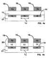
- a substrate 17 carries an underlying layer 15 therein.
- a surface 14 of the underlying layer 15 is depicted as being flush with an upper surface 12 of the substrate 17 .
- the underlying layer 15 and the surface 14 need not be flush with each other and the underlying layer 15 can have a non-planar surface.
- the substrate 17 can be a layer of a dielectric material such as silicon oxide ( SiO 2 ) or silicon nitride ( Si 3 N 4 ), for example.
- the underlying layer 15 includes a feature size L F that is substantially greater than or equal to a lithography limit ⁇ L of a lithographic system used to pattern the underlying layer 15.
- the underlying layer 15 can be formed in the substrate 17 by a variety of methods that are well understood in the microelectronics art including chemical mechanical planarization (CMP) or a damascene process if it is desired to have a substantially planar and flush surfaces for underlying layer 15 and the surface 14.
- CMP chemical mechanical planarization
- damascene process if it is desired to have a substantially planar and flush surfaces for underlying layer 15 and the surface 14.
- the underlying layer 15 may be patterned into discrete segments as depicted in FIG. 1 or the underlying layer 15 may be a continuous layer (see reference numeral 15 in FIG. 8b ) . In either case, the underlying layer 15 includes the feature size L F that is substantially greater than or equal to a lithography limit ⁇ L .
- the underlying layer 15 can be an electrically conductive material. Suitable materials for the underlying layer 15 include but are not limited to a metal, aluminum ( Al ), tungsten ( W ), titanium ( Ti ), molybdenum ( Mo ), and copper ( Cu ).
- a first polymer layer 11 is deposited on the surface 14 of the underlying layer 15.
- the first polymer layer 11 need not be photo active.
- the first polymer layer 11 has a first etch rate when the first polymer layer 11 is isotropically etched.
- a second polymer layer 13 is deposited on the first polymer layer 11.
- the second polymer layer 13 must be photo active so that the second polymer layer 13 can be photolithographically patterned.
- the second polymer layer 13 has a second etch rate when the second polymer layer 13 is isotropically etched.
- the first etch rate is preselected to be faster than the second etch rate when the first and second polymer layers ( 11 , 13 ) are isotropically etched.
- the first etch rate of the first polymer layer 11 can be at least about 10.0% faster than the second etch rate of the second polymer layer 13.
- the first etch rate of the first polymer layer 11 can be from about 10.0% faster to about 20.0% faster than the second etch rate. That is, a lateral etch rate of the first polymer layer 11 can be from about 10.0% faster to about 20.0% faster than a lateral etch rate of the second polymer layer 13 when the first and second polymer layers ( 11, 13 ) are isotropically etched.
- the aforementioned values are an example only and the relative differences between the first etch rate and the second etch rate are not limited to those values.
- the first polymer layer 11 and the second polymer layer 13 can be photo active polymers, although the first polymer layer 11 need not necessarily be a photo active material. In contrast, the second polymer layer 13 must be a photo active material such as a photo active photoresist material, for example.
- the second polymer layer 13 is lithographically patterned.
- a mask 21 having a feature 23 thereon, with a mask feature size L M that is greater than or equal to a lithography limit ⁇ L of a lithographic system used to pattern the second polymer layer 13 is illuminated by light ( 35, 37 ) from a light source (not shown).
- the mask feature size L M can be substantially equal to the feature size L F .
- a portion of the light 37 is blocked by the feature 23 while another portion of the light 35 passes through the mask 21 and exposes the second polymer layer 13 .
- a portion of the second polymer layer 13 that is not exposed by the light 35 defines an etch mask (see reference numeral 19 in FIG. 4a ) in the second polymer layer 13 .
- a material for the second polymer layer 13 can be selected such that those portions of the second polymer layer 13 that are exposed to the light 35 define the etch mask 19.
- the etch mask 19 has a feature size L F that is within the lithography limit ⁇ L (i.e. L F ⁇ ⁇ L ) of a lithographic system used to pattern the etch mask 19.
- the second polymer layer 13 is anisotropically etched, typically in a photoresist developer solution, to dissolve all of the second polymer layer 13 except the etch mask 19 .
- the etching is continued until those portions of the first polymer layer 11 that are not covered by the etch mask 19 are also dissolved.
- the etch mask 19 and the first polymer layer 11 form a dual-polymer stacked layer 22 that extends outward of the underlying layer 15 .
- a developer, a solvent, or reactive ion etching can be used to anisotropically etch the first and second polymer ( 11, 13 ) layers, for example.
- the first polymer layer 11 and the etch mask 19 are isotropically etched. As the isotropic etching proceeds, the first polymer layer 11 dissolves in a substantially lateral direction R L1 at a faster rate than the etch mask 19 which also dissolves in a substantially lateral direction R L2 . Furthermore, as the first polymer layer 11 dissolves, it also recedes along the surface 14 of the underlying layer 15 and defines an exposed portion E that is not covered by the first polymer layer 11. The first polymer layer 11 also recedes along the etch mask 19 and defines an undercut portion U thereon that is not covered by the first polymer layer 11 . The faster rate of recession of the first polymer layer 11 relative to the slower recession rate of the etch mask 19 results in the first polymer layer 11 narrowing with respect to the feature size L F .
- the first polymer layer 11 and the etch mask 19 can be isotropically etched using an isotropic etching process that includes but is not limited to wet etching, plasma etching, and etching in a plasma comprising an oxygen ( O 2 ) gas.
- an isotropic etching process that includes but is not limited to wet etching, plasma etching, and etching in a plasma comprising an oxygen ( O 2 ) gas.
- other gases including but not limited to argon ( Ar ) gas, helium ( He ) gas, and a fluorine ( F ) containing gas can be added individually or in combination to the oxygen ( O 2 ) gas.
- the fluorine containing gas can include but is not limited to CF 4 , CHF 3 , C 4 F 8 , or SF 6 .
- the isotropic etching continues until the first polymer layer 11 has dissolved to a sub-lithographic feature size S F that is less than the feature size L F . Because of the differences in the first and second etch rates of the first polymer layer 11 and the etch mask 19, the etch mask 19 recedes a distance D 2 and the first polymer layer 11 recedes a distance D 1 that is greater than D 2 . For purposes of illustration, both D 1 and D 2 are measured relative to an outline 19' (shown in dashed line) that represents an outline of the first polymer layer 11 and the etch mask 19 prior to the isotropic etching.
- the final value for the sub-lithographic feature size S F will be application dependent and can vary due to a number of factors including the materials selected for the first and second polymer layers ( 11, 13 ) and the conditions and materials selected for the isotropic etch process.
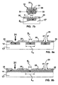
- the final value of the sub-lithographic feature size S F should be selected so that it is not less than a minimum value that would result in breakage or toppling of the first polymer layer 11 due to the mass of the etch mask 19 or the combined mass of the etch mask 19 and a dielectric layer 25 (see FIGS. 7a and 7b ) .
- a dielectric layer 25 is deposited on the exposed portion E of the underlying layer 15 and on substantially all of the etch mask 19; however, the dielectric layer 25 does not cover the undercut portion U of the etch mask 19 .
- the dielectric layer 25 forms a via sidewall 27 that is positioned adjacent to the first polymer layer 11.
- the dielectric layer 25 can be made from a material including but not limited to silicon oxide ( SiO 2 ), aluminum oxide ( Al 2 O 3 ), zirconium oxide ( ZrO 2 ), yttrium oxide ( Y 2 O 3 ), silicon nitride ( Si 3 N x ), and aluminum nitride ( AIN ), for example.
- the dielectric layer 25 covers a top surface 31 and side surfaces 33 of the etch mask 19, but the dielectric layer 25 does not cover a bottom surface 39 of the etch mask 19 .
- the bottom surface 39 is coincident with the undercut portion U .
- the dielectric layer 25 can be deposited using chemical vapor deposition (CVD) or physical vapor deposition (PVD). Examples of PVD are sputtering or thermal evaporation.
- the deposition process is a low temperature process when the materials selected for the first and second polymer layers ( 11 , 13 ) are polymers that could degrade under a high temperature deposition process. Examples of polymers that can degrade at high temperatures include photoresist materials. Accordingly, the temperature selected for depositing the dielectric layer 25 should not exceed a temperature limit that would damage or destroy the first and second polymer layers ( 11, 13 ).
- the first polymer layer 11 and the etch mask 19 are lifted-off of the surface 14 of the underlying layer 15 to define a via 31 including a minimum feature size that is substantially equal to the sub-lithographic feature size S F . That is, the via 31 has a sub-lithographic feature size.
- the lifting-off of first polymer layer 11 and the etch mask 19 can be accomplished using a solvent that dissolves the material used for the first polymer layer 11 or by using a solvent that dissolves the first polymer layer 11 and the etch mask 19 .
- the via 31 has a bottom surface 29 that is coincident with the surface 14 and sidewall surfaces 27 that extended outward of the bottom surface 29.
- the underlying layer 15 can be a continuous layer as is depicted in FIG. 8b where there are a plurality of the sub-lithographic sized vias 31 formed on the underlying layer 15.
- the underlying layer 15 includes the feature size L F that is substantially greater than or equal to a lithography limit ⁇ L .
- the actual value of the lithography limit ⁇ L will be application dependent and can depend on factors including the photolithographic system used and the wavelength of light used, for example. In one embodiment of the present invention, the lithography limit ⁇ L can be greater than or equal to about 0.10 ⁇ m.
- the actual value for the sub-lithographic feature size S F will also be application dependent and can depend on factors including the material for the first polymer layer 11 and an etch time for the isotropic etch process.
- the sub-lithographic feature size S F can be less than about 0.06 ⁇ m.
Claims (14)
- Ein Verfahren zum Herstellen eines unterlithographisch dimensionierten Durchgangslochs (31), das folgende Schritte aufweist:Aufbringen einer ersten Polymerschicht (11) auf einer Oberfläche (14) einer darunter liegenden Schicht (15), wobei die erste Polymerschicht (11) eine erste Ätzrate bei einem isotropen Ätzmittel aufweist;Aufbringen einer zweiten Polymerschicht (13) auf der ersten Polymerschicht (11), wobei die zweite Polymerschicht (13) photoaktiv ist und eine zweite Ätzrate bei dem gleichen isotropen Ätzmittel aufweist, wobei die erste Ätzrate vorausgewählt ist, um schneller zu sein als die zweite Ätzrate, wenn die erste und die zweite Polymerschicht (11, 13) isotrop geätzt werden;Strukturieren der zweiten Polymerschicht (13), um eine Ätzmaske (19) darin zu definieren, wobei die Ätzmaske (19) eine Merkmalsgröße umfasst, die innerhalb einer Lithographiegrenze (λL) eines lithographischen Systems liegt, das zum Strukturieren verwendet wird;anisotropes Ätzen der ersten Polymerschicht (11), um alle Abschnitte der ersten Polymerschicht (11) zu entfernen, die nicht durch die Ätzmaske (19) bedeckt sind;isotropes Ätzen der ersten Polymerschicht (11) und der Ätzmaske (19), derart, dass die erste Polymerschicht (11) sich in einer im Wesentlichen lateralen Richtung (RL1) mit einer schnelleren Rate als die Ätzmaske (19) auflöst, wobei die erste Polymerschicht (11) entlang der Oberfläche (14) der darunter liegenden Schicht (15) zurückgeht, wobei eine freiliegende Oberfläche (E) darauf definiert wird, und entlang der Ätzmaske (19) zurückgeht, wobei ein Unterschneidungsabschnitt (U) darauf definiert wird, und wobei das Ätzen fortgeführt wird, bis die erste Polymerschicht (11) sich zu einer unterlithographischen Merkmalsgröße (SF) aufgelöst hat, die geringer ist als die Lithographiegrenze (λL);Aufbringen einer dielektrischen Schicht (25) auf dem freiliegenden Abschnitt (E) der darunter liegenden Schicht (15) und auf im Wesentlichen der gesamten Ätzmaske (19) mit Ausnahme des Unterschneidungsabschnitts (U), wobei die dielektrische Schicht (25) eine Durchgangslochseitenwand (27) bildet, die benachbart zu der ersten Polymerschicht (11) positioniert ist; undAbheben der ersten Polymerschicht (11) und der Ätzmaske (19), um ein Durchgangsloch (31) zu definieren, das eine minimale Merkmalsgröße umfasst, die im Wesentlichen gleich der unterlithographischen Merkmalsgröße (SF) ist.
- Das Verfahren gemäß Anspruch 1, bei dem die darunter liegende Schicht (15) ein elektrisch leitfähiges Material ist.
- Das Verfahren gemäß Anspruch 2, bei dem das elektrisch leitfähige Material ein Material ist, das aus der Gruppe ausgewählt ist, die ein Metall, Aluminium, Wolfram, Titan, Molybdän und Kupfer umfasst.
- Das Verfahren gemäß einem der vorhergehenden Ansprüche, bei dem die Lithographiegrenze (λL) größer oder gleich etwa 0,10 µm ist.
- Das Verfahren gemäß einem der vorhergehenden Ansprüche, bei dem die unterlithographische Merkmalsgröße (SF) weniger als etwa 0,06 µm beträgt.
- Das Verfahren gemäß einem der vorhergehenden Ansprüche, bei dem die unterlithographische Merkmalsgröße (SF) um einen Faktor in einem Bereich von etwa 0,40 bis etwa 0,80 geringer als die Lithographiegrenze (λL) ist.
- Das Verfahren gemäß einem der vorhergehenden Ansprüche, bei dem die dielektrische Schicht (25) mittels chemischer Aufdampfung, physikalischer Aufdampfung, Sputtern oder thermischer Aufdampfung aufgebracht wird.
- Das Verfahren gemäß einem der vorhergehenden Ansprüche, bei dem der Abhebeschritt ein Auflösen der ersten Polymerschicht (11) und der Ätzmaske (19) in einem Lösungsmittel aufweist.
- Das Verfahren gemäß einem der vorhergehenden Ansprüche, bei dem der Isotropätzschritt ein Nassätzen, ein Plasmaätzen oder ein Ätzen in einem Plasma aufweist, das ein Sauerstoffgas aufweist.
- Das Verfahren gemäß Anspruch 9, bei dem das Ätzen in einem Plasma stattfindet, das auch eines oder mehr von Argongas, Heliumgas oder einem Fluor enthaltenden Gas aufweist.
- Das Verfahren gemäß einem der vorhergehenden Ansprüche, bei dem die dielektrische Schicht (25) Siliziumoxid, Aluminiumoxid, Zirkoniumoxid, Yttriumoxid, Siliziumnitrid oder Aluminiumnitrid aufweist.
- Das Verfahren gemäß einem der vorhergehenden Ansprüche, bei dem das erste Ätzen der ersten Polymerschicht (11) um zumindest 10,0% schneller ist als die zweite Ätzrate der zweiten Polymerschicht (13).
- Das Verfahren gemäß einem der vorhergehenden Ansprüche, bei dem die erste Polymerschicht (11) ein nicht photoaktives Polymermaterial oder ein photoaktives Polymermaterial aufweist.
- Das Verfahren gemäß einem der vorhergehenden Ansprüche, bei dem die zweite Polymerschicht (13) ein photoaktives Photoresistmaterial aufweist.
Applications Claiming Priority (2)
| Application Number | Priority Date | Filing Date | Title |
|---|---|---|---|
| US133605 | 1998-08-13 | ||
| US10/133,605 US6673714B2 (en) | 2002-04-25 | 2002-04-25 | Method of fabricating a sub-lithographic sized via |
Publications (3)
| Publication Number | Publication Date |
|---|---|
| EP1359609A2 EP1359609A2 (de) | 2003-11-05 |
| EP1359609A3 EP1359609A3 (de) | 2004-03-31 |
| EP1359609B1 true EP1359609B1 (de) | 2005-08-17 |
Family
ID=29215620
Family Applications (1)
| Application Number | Title | Priority Date | Filing Date |
|---|---|---|---|
| EP03252512A Expired - Lifetime EP1359609B1 (de) | 2002-04-25 | 2003-04-22 | Verfahren zur Herstellung einer sub-lithographischen Durchgangsleitung |
Country Status (5)
| Country | Link |
|---|---|
| US (1) | US6673714B2 (de) |
| EP (1) | EP1359609B1 (de) |
| JP (1) | JP2003338458A (de) |
| CN (1) | CN1453640A (de) |
| DE (1) | DE60301295T2 (de) |
Families Citing this family (14)
| Publication number | Priority date | Publication date | Assignee | Title |
|---|---|---|---|---|
| US6916511B2 (en) * | 2002-10-24 | 2005-07-12 | Hewlett-Packard Development Company, L.P. | Method of hardening a nano-imprinting stamp |
| US7384727B2 (en) * | 2003-06-26 | 2008-06-10 | Micron Technology, Inc. | Semiconductor processing patterning methods |
| US7026243B2 (en) * | 2003-10-20 | 2006-04-11 | Micron Technology, Inc. | Methods of forming conductive material silicides by reaction of metal with silicon |
| US6969677B2 (en) * | 2003-10-20 | 2005-11-29 | Micron Technology, Inc. | Methods of forming conductive metal silicides by reaction of metal with silicon |
| US7462292B2 (en) * | 2004-01-27 | 2008-12-09 | Hewlett-Packard Development Company, L.P. | Silicon carbide imprint stamp |
| US7060625B2 (en) * | 2004-01-27 | 2006-06-13 | Hewlett-Packard Development Company, L.P. | Imprint stamp |
| US7153769B2 (en) * | 2004-04-08 | 2006-12-26 | Micron Technology, Inc. | Methods of forming a reaction product and methods of forming a conductive metal silicide by reaction of metal with silicon |
| US7241705B2 (en) * | 2004-09-01 | 2007-07-10 | Micron Technology, Inc. | Methods of forming conductive contacts to source/drain regions and methods of forming local interconnects |
| DE102005008478B3 (de) | 2005-02-24 | 2006-10-26 | Infineon Technologies Ag | Verfahren zur Herstellung von sublithographischen Strukturen |
| KR100869359B1 (ko) * | 2006-09-28 | 2008-11-19 | 주식회사 하이닉스반도체 | 반도체 소자의 리세스 게이트 제조 방법 |
| JP5349404B2 (ja) * | 2010-05-28 | 2013-11-20 | 株式会社東芝 | パターン形成方法 |
| NL2007452A (en) * | 2010-12-08 | 2012-06-11 | Asml Holding Nv | Electrostatic clamp, lithographic apparatus and method of manufacturing an electrostatic clamp. |
| WO2017116858A1 (en) * | 2015-12-30 | 2017-07-06 | Fujifilm Electronic Materials U.S.A., Inc. | Photosensitive stacked structure |
| CN109065445B (zh) * | 2018-07-13 | 2020-10-09 | 上海华力集成电路制造有限公司 | 金属栅极结构的制造方法 |
Family Cites Families (12)
| Publication number | Priority date | Publication date | Assignee | Title |
|---|---|---|---|---|
| JPS58130575A (ja) * | 1982-01-29 | 1983-08-04 | Hitachi Ltd | 電界効果トランジスタの製造方法 |
| JPS6229175A (ja) * | 1985-07-29 | 1987-02-07 | Nippon Telegr & Teleph Corp <Ntt> | 電界効果型トランジスタの製造方法 |
| US4670090A (en) * | 1986-01-23 | 1987-06-02 | Rockwell International Corporation | Method for producing a field effect transistor |
| DE3685495D1 (de) * | 1986-07-11 | 1992-07-02 | Ibm | Verfahren zur herstellung einer unteraetzten maskenkontur. |
| US4711701A (en) * | 1986-09-16 | 1987-12-08 | Texas Instruments Incorporated | Self-aligned transistor method |
| US4808545A (en) * | 1987-04-20 | 1989-02-28 | International Business Machines Corporation | High speed GaAs MESFET having refractory contacts and a self-aligned cold gate fabrication process |
| DE3879186D1 (de) * | 1988-04-19 | 1993-04-15 | Ibm | Verfahren zur herstellung von integrierten halbleiterstrukturen welche feldeffekttransistoren mit kanallaengen im submikrometerbereich enthalten. |
| KR910005400B1 (ko) * | 1988-09-05 | 1991-07-29 | 재단법인 한국전자통신연구소 | 다층레지스트를 이용한 자기정합형 갈륨비소 전계효과트랜지스터의 제조방법 |
| JPH06267843A (ja) * | 1993-03-10 | 1994-09-22 | Hitachi Ltd | パターン形成方法 |
| KR0146246B1 (ko) * | 1994-09-26 | 1998-11-02 | 김주용 | 반도체 소자 콘택 제조방법 |
| US5976920A (en) * | 1996-07-22 | 1999-11-02 | The United States Of America As Represented By The Secretary Of The Air Force | Single layer integrated metal process for high electron mobility transistor (HEMT) and pseudomorphic high electron mobility transistor (PHEMT) |
| US6036875A (en) * | 1997-02-20 | 2000-03-14 | Advanced Micro Devices, Inc. | Method for manufacturing a semiconductor device with ultra-fine line geometry |
-
2002
- 2002-04-25 US US10/133,605 patent/US6673714B2/en not_active Expired - Lifetime
-
2003
- 2003-04-04 JP JP2003101055A patent/JP2003338458A/ja active Pending
- 2003-04-22 DE DE60301295T patent/DE60301295T2/de not_active Expired - Lifetime
- 2003-04-22 EP EP03252512A patent/EP1359609B1/de not_active Expired - Lifetime
- 2003-04-25 CN CN03122426A patent/CN1453640A/zh active Pending
Also Published As
| Publication number | Publication date |
|---|---|
| US6673714B2 (en) | 2004-01-06 |
| CN1453640A (zh) | 2003-11-05 |
| DE60301295D1 (de) | 2005-09-22 |
| DE60301295T2 (de) | 2006-08-10 |
| EP1359609A3 (de) | 2004-03-31 |
| US20030211729A1 (en) | 2003-11-13 |
| EP1359609A2 (de) | 2003-11-05 |
| JP2003338458A (ja) | 2003-11-28 |
Similar Documents
| Publication | Publication Date | Title |
|---|---|---|
| US6713396B2 (en) | Method of fabricating high density sub-lithographic features on a substrate | |
| US6759180B2 (en) | Method of fabricating sub-lithographic sized line and space patterns for nano-imprinting lithography | |
| US6110837A (en) | Method for forming a hard mask of half critical dimension | |
| EP1359609B1 (de) | Verfahren zur Herstellung einer sub-lithographischen Durchgangsleitung | |
| US5641610A (en) | Method for producing a multi-step structure in a substrate | |
| KR100272644B1 (ko) | 드라이에칭방법 | |
| US7105442B2 (en) | Ashable layers for reducing critical dimensions of integrated circuit features | |
| US5045150A (en) | Plasma etching using a bilayer mask | |
| US20050181604A1 (en) | Method for structuring metal by means of a carbon mask | |
| US6355979B2 (en) | Hard mask for copper plasma etch | |
| US6589880B2 (en) | Fine pattern formation method and semiconductor device or liquid crystal device manufacturing method employing this method | |
| US6399286B1 (en) | Method of fabricating reduced critical dimension for conductive line and space | |
| EP0076215B1 (de) | Schattenmaske für Abhebetechnik | |
| JP2003338458A5 (de) | ||
| KR100374955B1 (ko) | 반도체 장치의 제조 방법 | |
| JP4095588B2 (ja) | 集積回路にフォトリソグラフィ解像力を超える最小ピッチを画定する方法 | |
| EP0260201B1 (de) | Plasma-Ätzverfahren unter Verwendung eines zweischichtigen Musters | |
| WO2002043140A2 (en) | Imaging layer as hard mask for organic low-k materials | |
| KR20020024415A (ko) | 반도체 소자의 패턴 형성방법 | |
| US20080305635A1 (en) | Method for fabricating a pattern | |
| EP0647966A1 (de) | Halbleiterbauelement mit Leitermuster und Verfahren zur Herstellung | |
| KR100632422B1 (ko) | 반도체 기판내에 구조를 형성하는 방법 | |
| CN111834212A (zh) | 半导体器件及其形成方法 | |
| US6548413B1 (en) | Method to reduce microloading in metal etching | |
| US20230245890A1 (en) | Pitch Scaling in Microfabrication |
Legal Events
| Date | Code | Title | Description |
|---|---|---|---|
| PUAI | Public reference made under article 153(3) epc to a published international application that has entered the european phase |
Free format text: ORIGINAL CODE: 0009012 |
|
| AK | Designated contracting states |
Kind code of ref document: A2 Designated state(s): AT BE BG CH CY CZ DE DK EE ES FI FR GB GR HU IE IT LI LU MC NL PT RO SE SI SK TR |
|
| AX | Request for extension of the european patent |
Extension state: AL LT LV MK |
|
| RIN1 | Information on inventor provided before grant (corrected) |
Inventor name: ANTHONY, THOMAS C. Inventor name: TRAN, LUNG T. Inventor name: LEE, HEON |
|
| PUAL | Search report despatched |
Free format text: ORIGINAL CODE: 0009013 |
|
| AK | Designated contracting states |
Kind code of ref document: A3 Designated state(s): AT BE BG CH CY CZ DE DK EE ES FI FR GB GR HU IE IT LI LU MC NL PT RO SE SI SK TR |
|
| AX | Request for extension of the european patent |
Extension state: AL LT LV MK |
|
| RIC1 | Information provided on ipc code assigned before grant |
Ipc: 7H 01L 21/308 B Ipc: 7G 03F 7/095 B Ipc: 7H 01L 21/027 A |
|
| 17P | Request for examination filed |
Effective date: 20040607 |
|
| AKX | Designation fees paid |
Designated state(s): DE GB |
|
| GRAP | Despatch of communication of intention to grant a patent |
Free format text: ORIGINAL CODE: EPIDOSNIGR1 |
|
| GRAS | Grant fee paid |
Free format text: ORIGINAL CODE: EPIDOSNIGR3 |
|
| GRAA | (expected) grant |
Free format text: ORIGINAL CODE: 0009210 |
|
| AK | Designated contracting states |
Kind code of ref document: B1 Designated state(s): DE GB |
|
| REG | Reference to a national code |
Ref country code: GB Ref legal event code: FG4D |
|
| REF | Corresponds to: |
Ref document number: 60301295 Country of ref document: DE Date of ref document: 20050922 Kind code of ref document: P |
|
| PLBE | No opposition filed within time limit |
Free format text: ORIGINAL CODE: 0009261 |
|
| STAA | Information on the status of an ep patent application or granted ep patent |
Free format text: STATUS: NO OPPOSITION FILED WITHIN TIME LIMIT |
|
| 26N | No opposition filed |
Effective date: 20060518 |
|
| REG | Reference to a national code |
Ref country code: GB Ref legal event code: 732E Free format text: REGISTERED BETWEEN 20110203 AND 20110209 |
|
| REG | Reference to a national code |
Ref country code: DE Ref legal event code: R081 Ref document number: 60301295 Country of ref document: DE Owner name: SAMSUNG ELECTRONICS CO., LTD., KR Free format text: FORMER OWNER: HEWLETT-PACKARD DEVELOPMENT CO., L.P., HOUSTON, US Effective date: 20110426 Ref country code: DE Ref legal event code: R081 Ref document number: 60301295 Country of ref document: DE Owner name: SAMSUNG ELECTRONICS CO., LTD., SUWON-SI, KR Free format text: FORMER OWNER: HEWLETT-PACKARD DEVELOPMENT COMPANY, L.P., HOUSTON, TEX., US Effective date: 20110426 |
|
| PGFP | Annual fee paid to national office [announced via postgrant information from national office to epo] |
Ref country code: GB Payment date: 20220310 Year of fee payment: 20 |
|
| PGFP | Annual fee paid to national office [announced via postgrant information from national office to epo] |
Ref country code: DE Payment date: 20220316 Year of fee payment: 20 |
|
| REG | Reference to a national code |
Ref country code: DE Ref legal event code: R071 Ref document number: 60301295 Country of ref document: DE |
|
| REG | Reference to a national code |
Ref country code: GB Ref legal event code: PE20 Expiry date: 20230421 |
|
| PG25 | Lapsed in a contracting state [announced via postgrant information from national office to epo] |
Ref country code: GB Free format text: LAPSE BECAUSE OF EXPIRATION OF PROTECTION Effective date: 20230421 |