EP1359390A1 - Dispositif et procédé de controle automatique de l'état de surface de plaque par mesure de vitesse de collage - Google Patents
Dispositif et procédé de controle automatique de l'état de surface de plaque par mesure de vitesse de collage Download PDFInfo
- Publication number
- EP1359390A1 EP1359390A1 EP03291030A EP03291030A EP1359390A1 EP 1359390 A1 EP1359390 A1 EP 1359390A1 EP 03291030 A EP03291030 A EP 03291030A EP 03291030 A EP03291030 A EP 03291030A EP 1359390 A1 EP1359390 A1 EP 1359390A1
- Authority
- EP
- European Patent Office
- Prior art keywords
- plates
- bonding
- source
- wave
- passage
- Prior art date
- Legal status (The legal status is an assumption and is not a legal conclusion. Google has not performed a legal analysis and makes no representation as to the accuracy of the status listed.)
- Granted
Links
Images
Classifications
-
- G—PHYSICS
- G01—MEASURING; TESTING
- G01B—MEASURING LENGTH, THICKNESS OR SIMILAR LINEAR DIMENSIONS; MEASURING ANGLES; MEASURING AREAS; MEASURING IRREGULARITIES OF SURFACES OR CONTOURS
- G01B11/00—Measuring arrangements characterised by the use of optical techniques
- G01B11/30—Measuring arrangements characterised by the use of optical techniques for measuring roughness or irregularity of surfaces
- G01B11/306—Measuring arrangements characterised by the use of optical techniques for measuring roughness or irregularity of surfaces for measuring evenness
-
- H—ELECTRICITY
- H10—SEMICONDUCTOR DEVICES; ELECTRIC SOLID-STATE DEVICES NOT OTHERWISE PROVIDED FOR
- H10P—GENERIC PROCESSES OR APPARATUS FOR THE MANUFACTURE OR TREATMENT OF DEVICES COVERED BY CLASS H10
- H10P74/00—Testing or measuring during manufacture or treatment of wafers, substrates or devices
-
- H—ELECTRICITY
- H10—SEMICONDUCTOR DEVICES; ELECTRIC SOLID-STATE DEVICES NOT OTHERWISE PROVIDED FOR
- H10P—GENERIC PROCESSES OR APPARATUS FOR THE MANUFACTURE OR TREATMENT OF DEVICES COVERED BY CLASS H10
- H10P74/00—Testing or measuring during manufacture or treatment of wafers, substrates or devices
- H10P74/20—Testing or measuring during manufacture or treatment of wafers, substrates or devices characterised by the properties tested or measured, e.g. structural or electrical properties
- H10P74/203—Structural properties, e.g. testing or measuring thicknesses, line widths, warpage, bond strengths or physical defects
Definitions
- the present invention relates generally to the treatment of materials, and more particularly substrates for electronics, optics or optoelectronics.
- the invention relates to a device for characterizing the bonding speed between two sheets of material.
- the invention also relates to a method for such a device.
- Such plates generally have a disk-like outline of which the thickness is typically of the order of a few hundred microns.
- These plates can be glued in pairs to form multilayer structures, the two plates glued together can be in different materials.
- This time is called "collage time”.
- said glue wave can be viewed at through plates by transmitting infrared radiation from a source placed under the slice, the user observing this slice from above (by means such as a screen rendering the image provided by a infrared camera located above the edge).
- the bonding speed is representative of the surface state of plates: a high bonding speed indicates a good surface finish, while a lower bonding speed indicates the presence of defects and / or impurities on the surface of the plates.
- the surfaces of the plates at the end of a chain of manufacturing have some defects and residues that are both of a nature chemical (mainly OH bonds with the superficial particles of plates) and of a mechanical nature (typically roughness defects, presence of abrasive particles and superficial metal contaminants).
- a nature chemical mainly OH bonds with the superficial particles of plates
- a mechanical nature typically roughness defects, presence of abrasive particles and superficial metal contaminants.
- the characterization of the bonding speed can not currently be performed only manually, on a dedicated device.
- An object of the invention is to overcome this limitation.
- the invention proposes according to a first aspect a plate surface condition control device implementing a measurement of bonding speed of two plates at an interface of bonding defined between the two plates, characterized in that the device comprises means for automatically detecting start of gluing and means for automatically detecting the passage of a sticking wave.
- the invention also proposes the application of a device or method according to one of the above aspects, for checking the surface condition of medium thickness plate included between a few micrometers to a few millimeters.
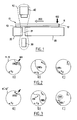
- a slice 10 consists of two plates 11 and 12 contiguous with each other, so as to define between they an interface called collage 13.
- the wafer 10 is placed on a gluing support 20.
- FIG. 1 is represented very schematic: this device can actually also include all micro-mechanisms mentioned in the introduction to this text concerning automatic gluing devices known.
- the invention can be implemented by adapting such a device of automatic bonding of known type.
- micro-mechanisms which can be placed above and / or below the plates
- micro-mechanisms are not shown on the figures.
- the surface of the support 20 receiving the wafer 10 must be particularly planar, especially if we study plates 11 and 12 having a surface important and a thickness of the order of a few microns.
- a poor flatness of the support 20 can lead to distortions of the plate 12 relative to the plate 11, and thus disturb the slice 10 at the gluing interface 13.
- the source 30 directs its radiation towards the sensor 40, through the opening 21.
- This radiation is intercepted by the slice 10 when it is in position on the device.
- the properties of the materials constituting the slice 10, and radiation from the source 30, are chosen so that a part significant amount of this radiation passes through the slice and that this part transmitted through the slice reaches the sensor 40.
- the source 30 is preferably a white lamp.
- the emission of the source 30 preferably comprises a spectrum infrared waves.
- the sensor 40 is preferably an optoelectronic device.
- the opening 21 made in the support 20 acts as a window electromagnetic and therefore allows the emitted electromagnetic radiation by the source 30 to cross the support 20 and to be detected by the sensor 40.
- the opening 21 passes through the support 20 at a location X of this support which is located next to slice 10 when it is positioned on the device.
- the opening 21 must be wide enough to avoid disturbances too much of the electromagnetic waves emitted by the source 30.
- These disturbances may, for example, be a significant loss of signal by reflection on the face of the support 20 closest to the source 30.
- These disturbances can also be diffractions and / or absorptions of the waves.
- the opening 21 must also be sufficiently narrow to overcome the presence of any material surrounding the plates, specific to the device automatic gluing of plates.
- the width of the opening 21 is typically of the order of a few millimeters.
- each opening can be traversed by the radiation of the source 30 (thanks to suitable separation and return mirrors), for after crossing the edge at the place concerned by the opening, at sensor 40 (always using separation and removal mirrors adapted for this purpose).
- the device according to the invention operates as follows:
- a gluing piston contacts the two plates 11 and 12 at the level of the interface 13 by exerting at a given location X1 of the surface of the slice 10, an initial pressure 100 sufficient to initiate a bond between the two plates.
- This piston is controlled by an instruction sent by a unit central processing unit, which is connected to the piston and which stores the moment of start of collage.
- the start time of bonding is determined by a bonding start detector associated with the piston.
- This automatic start-of-glue detector can be for example a piezoelectric transducer.
- the start of collage is triggered automatically following an initial instruction, and an associated start time of collage is stored.
- the initial instruction can be provided by an operator or by a device automatically set, for example, according to time sequences managed by a clock.
- the source 30 is activated so as to permanently transmit a radiation directed through the wafer 10 to the sensor 40 associated with the source.
- the collage then spreads over the entire surface of the plates, at the level of of the interface 13, according to a 200 propagation wave bonding.
- the sensor 40 When the bonding wave 200 reaches the "X" position of the slice, that is to say at the opening 21, the sensor 40 then detects a change in the electromagnetic signal that it receives from the source 30 via the slice 10, compared to the reference signal that it received from this same slice before passing the bonding wave.
- This change of electromagnetic signal typically translates a optical characteristic of the radiation of the source, and may in particular correspond to a change of contrast revealing an appearance of binding forces between the two plates 11 and 12, following the establishment of hydrogen forces between the two plates.
- the optical waves emitted by the source 30 have a spectrum lying preferentially in the infrared.
- the sensor 40 detects the passage of the bonding wave at the location X of the plates which is located at the level of the opening 21, it emits a signal of detection of passage from the bonding front to the treatment unit to which it is also connected.
- This processing unit then calculates the bonding time between the memorized start time of collage, and the time of passage from front to collage that physically corresponds to the establishment of a collage between plates.
- the processing unit is also connected to a clock.
- this unit automatically deduces a gluing speed, which is characteristic of the surface state of plates 11 and 12 between measuring locations X1 and X.
- the support 20 is traversed by a plurality of openings 21 distributed on the support 20 so as to be able to detect in different places of the plates 11 and 12 the passage of the wave of collage, and allow the processing unit to calculate for each of these places a bonding speed.
- the senor includes means for discriminating the different signals (these signals being able to example have specific wavelengths depending on the source emission, or more generally of the opening traversed).
- the processing unit can calculate different "instantaneous" gluing speeds, for different openings.
- the processing unit is connected to all the sensors 40, and that it receives all the sticking wave signals different places associated with an opening of the support 20.
- processing unit can thus also calculate speeds of collage between two of these places, by treating the time difference of passage of the bonding wave at both locations (the distances between different locations associated with an opening of the support being known and stored in the processing unit).
- each source 30 can in particular be associated with each source 30 a respective sensor 40, aligned with the source and the opening, the sensor and the source being both sides of the opening 21.
- detection assemblies 50 are then obtained. automatic, each being similar to the assembly 50 shown in FIG. detection sets being arranged in such a way as to make it possible to determine different bonding speeds in different regions of the slice 10, according to the progress state of the bonding wave 200 on the interface 13.
- the invention is not limited to the detection means schematized on the figure 1.
- the invention can implement any automatic detection means start of gluing and any means of automatic detection of moment of passage of a bonding front.
- detection sets equivalent to the assembly 50, with a source of radiation directed to a place predetermined amount of the slice, said location reflecting the radiation of the source to an associated sensor.
- the means for automatically detecting the moment of passage of the front collage may also include one or more detection sets automatically, such that each of them is able to detect a moment of bonding to a local region of the interface 13.
- a bonding wave is initiated to produce a forehead 200a (FIG. 2a), then propagates (front 200b - FIG. 2b) and ends (front 200c) at a place opposite to the initial pressure point 100 (Figure 2c).
- the detection assembly 50 then will be preferentially placed near the wavefront 200c at X2, and the bonding speed will be determined on the basis of the time put by the wave of collage to travel the distance separating the X1 location from the pressure 100 and the X2 where the end of detection point is located. bonding.
- a pressure 100 similar to the pressure 100 of FIG. 2 is exerted at the same location X1 on plates 11 'and 12' which are similar to plates 11 and 12 of FIG.
- the propagation follows several steps 200a '( Figure 3a), 200b' ( Figure 3b) and 200c '(FIG. 3c) respectively corresponding to the steps 200a, 200b and 200c of Figure 2.
- a device according to the invention comprising several openings 21 or, in a more general case, in a variant of a Device according to the invention implementing several detection assemblies automatic gluing moment, the detections being thus performed locally on the whole surface of the slice 10, one would then be able to determine locally kinetics of plate bonding, and so to get more information on the quality of the plate surface condition, but also information on the nature and location of surface defects potential.
- Such a device or method according to the invention applies preferentially to plates intended for microelectronics, ie plates of several centimeters in diameter for thicknesses of the order of micron or several tens of microns.
- This type of plate then contains at least one semiconductor material, such as silicon.
- these plates comprise SOI type, acronym for "Silicon On Insulator”.
- One of the two plates (11 or 12) may not be intended for micro-electronic application, and can for example play the role of a plate of particularly flat reference.
- the measurements made by the device according to the invention can remain memorized in the processing unit, as well as the parameters derived from it (speed lift-off, ).
Landscapes
- Physics & Mathematics (AREA)
- General Physics & Mathematics (AREA)
- Testing Or Measuring Of Semiconductors Or The Like (AREA)
- Investigating Or Analysing Materials By Optical Means (AREA)
- Investigating Materials By The Use Of Optical Means Adapted For Particular Applications (AREA)
Abstract
Description
- mettre en contact les surfaces respectives de ces plaques, de manière à constituer une tranche ayant la forme générale d'un disque et comprenant les deux plaques accolées,
- comprimer la tranche formée par les deux plaques en un point quelconque de cette tranche,
- mesurer le temps nécessaire à l'établissement d'une liaison entre les deux plaques, suite à cette compression.
- au moins un bain basique. Cette étape a pour objectif de développer l'hydrophylie des plaques, en créant à la surface desdites plaques des liaisons de type OH,
- puis un bain acide, afin d'éliminer de la surface des plaques les éléments contaminants (en particulier métalliques) qui ont pu être amenés par les étapes antérieures de traitement des plaques (et en particulier par le bain basique).
- les moyens de détection automatique de passage d'une onde de collage comprennent une source de rayonnement électromagnétique et un capteur apte à détecter au moins une partie du spectre du rayonnement électromagnétique émis par la source, le capteur étant disposé de manière à recueillir le rayonnement issu d'un endroit de mesure déterminé de l'interface de collage,
- le dispositif comprend une unité de traitement à laquelle sont reliés les moyens de détection automatique de début de collage et les moyens de détection automatique de passage d'une onde de collage,
- l'unité de traitement est apte à calculer des vitesses instantanées de collage, pour chaque endroit de mesure de l'interface de collage,
- le capteur est apte à détecter un changement d'une caractéristique de l'onde électromagnétique qu'il reçoit de la source par l'intermédiaire d'au moins un endroit de mesure,
- le changement de caractéristique de l'onde électromagnétique est un changement de contraste,
- les moyens de détection automatique de passage d'une onde de collage comprennent en outre, en association avec au moins un endroit de mesure, une ouverture respective traversant le support et laissant passer le rayonnement issu de la source afin que celui-ci traverse ensuite les plaques au niveau de l'endroit de mesure, pour que la partie du rayonnement issu de la source qui a été transmise au travers des plaques aboutisse au capteur,
- les moyens de détection comprennent au moins un ensemble de détection constitué d'une source électromagnétique, d'une ouverture et d'un capteur électromagnétique tels que la source et le capteur sont alignés de part et d'autre de l'ouverture,
- les moyens de détection automatique de passage d'une onde de collage comprennent en outre, en association avec au moins un endroit de mesure, une source de rayonnement électromagnétique dirigé vers l'endroit de mesure et réfléchi par les plaques vers un capteur associé,
- la source est de type lampe,
- le capteur est optoélectronique,
- le spectre électromagnétique émis par la source comprend le domaine des infrarouges,
- le dispositif comprend une pluralité d'ensembles de détection de passage d'onde de collage entre les deux plaques, associés respectivement à une pluralité d'endroits de mesure des plaques à contrôler, de sorte que chacun de ces ensembles autorise une détermination locale d'un moment de collage local au niveau de l'endroit de mesure associé,
- les moyens de détection automatique de moment de collage comprennent une pluralité d'ouvertures associées respectivement à des endroits de mesure, chaque ouverture autorisant une détection locale de moment de collage local au niveau de la région de détection associée.
- Acquisition automatique d'un moment de début de collage,
- Acquisition automatique d'un moment de passage d'une onde de collage,
- Détermination automatique d'une vitesse de collage à partir de ces deux acquisitions.
- les moments de passage d'une onde de collage sont acquis au niveau d'un endroit de mesure des plaques, à partir d'un changement d'une caractéristique d'une onde électromagnétique issue de l'endroit de mesure,
- le changement de caractéristique de l'onde électromagnétique est un changement de contraste,
- le spectre de l'onde électromagnétique comprend le domaine des infrarouges,
- plusieurs moments de passage local d'une onde de collage sont détectés respectivement en plusieurs endroits de mesure des plaques.
- la structure de plaque contrôlée comprend du silicium,
- la structure de plaque contrôlée comprend une structure de type SOI.
- La figure 1 représente schématiquement un dispositif conforme à l'invention,
- La figure 2 représente un exemple de progression dans le temps d'une onde de collage entre deux tranches accolées et définissant entre elles une interface de collage ne présentant pas de défauts,
- La figure 3 représente un exemple de progression dans le temps d'une onde de collage entre deux tranches accolées et définissant entre elles une interface de collage présentant un défaut.
- deux plaques « accolées » sont simplement disposées de manière à être en contact l'une avec l'autre, aucune liaison n'existant entre les plaques,
- alors que deux plaques « collées » sont en outre solidaires l'une de l'autre, des liaisons (par exemple du type hydrogène) existant entre les plaques.
- vers l'ouverture 21, en dirigeant le rayonnement selon l'axe de cette ouverture,
- puis de la tranche qui est traversée par le rayonnement vers la capteur 40.
Claims (22)
- Dispositif de contrôle de l'état de surface de plaque mettant en oeuvre une mesure de vitesse de collage de deux plaques (11, 12) au niveau (13) d'une interface de collage définie entre les deux plaques, caractérisé en ce que le dispositif comprend des moyens de détection automatique de début de collage et des moyens de détection automatique de passage d'une onde de collage.
- Dispositif selon la revendication précédente, caractérisé en ce que les moyens de détection automatique de passage d'une onde de collage comprennent une source (30) de rayonnement électromagnétique et un capteur (40) apte à détecter au moins une partie du spectre du rayonnement électromagnétique émis par la source (30), le capteur (40) étant disposé de manière à recueillir le rayonnement issu d'un endroit (X) de mesure déterminé de l'interface de collage.
- Dispositif selon la revendication précédente, caractérisé en ce que le dispositif comprend une unité de traitement à laquelle sont reliés les moyens de détection automatique de début de collage et les moyens de détection automatique de passage d'une onde de collage.
- Dispositif selon la revendication précédente, caractérisé en ce que l'unité de traitement est apte à calculer des vitesses instantanées de collage, pour chaque endroit de mesure de l'interface de collage.
- Dispositif selon l'une des trois revendications précédentes, caractérisé en ce que le capteur (40) est apte à détecter un changement d'une caractéristique de l'onde électromagnétique qu'il reçoit de la source (30) par l'intermédiaire d'au moins un endroit de mesure.
- Dispositif selon la revendication précédente, caractérisé en ce que le changement de caractéristique de l'onde électromagnétique est un changement de contraste.
- Dispositif selon l'une des cinq revendications précédentes, caractérisé en ce que les moyens de détection automatique de passage d'une onde de collage comprennent en outre, en association avec au moins un endroit de mesure, une ouverture respective traversant le support et laissant passer le rayonnement issu de la source afin que celui-ci traverse ensuite les plaques au niveau de l'endroit de mesure, pour que la partie du rayonnement issu de la source qui a été transmise au travers des plaques aboutisse au capteur.
- Dispositif selon la revendication précédente, caractérisé en ce que les moyens de détection comprennent au moins un ensemble (50) de détection constitué d'une source électromagnétique (30), d'une ouverture (21) et d'un capteur électromagnétique (40) tels que la source (30) et le capteur (40) sont alignés de part et d'autre de l'ouverture (21).
- Dispositif selon l'une des sept revendications précédentes, caractérisé en ce que les moyens de détection automatique de passage d'une onde de collage comprennent en outre, en association avec au moins un endroit de mesure, une source de rayonnement électromagnétique dirigé vers l'endroit de mesure et réfléchi par les plaques vers un capteur associé.
- Dispositif selon l'une des revendications précédentes, caractérisé en ce que la source (30) est de type lampe.
- Dispositif selon l'une des revendications précédentes, caractérisé en ce que le capteur (40) est optoélectronique.
- Dispositif selon l'une des revendications précédentes, caractérisé en ce que le spectre électromagnétique émis par la source (30) comprend le domaine des infrarouges.
- Dispositif selon l'une des onze revendications précédentes, caractérisé en ce que le dispositif comprend une pluralité d'ensembles (50) de détection de passage d'onde de collage entre les deux plaques, associés respectivement à une pluralité d'endroits de mesure des plaques à contrôler, de sorte que chacun de ces ensembles autorise une détermination locale d'un moment de collage local au niveau de l'endroit de mesure associé.
- Dispositif selon la revendication précédente en combinaison avec la revendication 7 ou 8, caractérisé en ce que les moyens de détection automatique de moment de collage comprennent une pluralité d'ouvertures (21) associées respectivement à des endroits de mesure, chaque ouverture (21) autorisant une détection locale de moment de collage local au niveau de la région de détection associée.
- Procédé de contrôle de l'état de surface de plaque mettant en oeuvre une mesure de vitesse de collage de deux plaques (11, 12) au niveau d'une interface de collage (13), caractérisé en ce que le procédé comprend les opérations suivantes :Acquisition automatique d'un moment de début de collage,Acquisition automatique d'un moment de passage d'une onde de collage,Détermination automatique d'une vitesse de collage à partir de ces deux acquisitions.
- Procédé selon la revendication précédente, caractérisé en ce que les moments de passage d'une onde de collage sont acquis au niveau d'un endroit de mesure des plaques (11, 12), à partir d'un changement d'une caractéristique d'une onde électromagnétique issue de l'endroit de mesure.
- Procédé selon la revendication précédente, caractérisé en ce que le changement de caractéristique de l'onde électromagnétique est un changement de contraste.
- Procédé selon l'une des deux revendications précédentes, caractérisé en ce que le spectre de l'onde électromagnétique comprend le domaine des infrarouges.
- Procédé selon l'une des trois revendications précédentes, caractérisé en ce que plusieurs moments de passage local d'une onde de collage sont détectés respectivement en plusieurs endroits de mesure des plaques.
- Application d'un dispositif selon l'une des revendications 1 à 14 ou d'un procédé selon l'une des revendications 15 à 19, pour le contrôle de l'état de surface de plaque d'épaisseur moyenne comprise entre un micromètre et quelques millimètres.
- Application selon la revendication précédente, caractérisée en ce que la structure de plaque contrôlée comprend du silicium.
- Application selon la revendication précédente, caractérisée en ce que la structure de plaque contrôlée comprend une structure de type SOI.
Applications Claiming Priority (2)
| Application Number | Priority Date | Filing Date | Title |
|---|---|---|---|
| FR0205427A FR2839147B1 (fr) | 2002-04-30 | 2002-04-30 | Dispositif et procede de controle automatique de l'etat de surface de plaque par mesure de vitesse de collage |
| FR0205427 | 2002-04-30 |
Publications (2)
| Publication Number | Publication Date |
|---|---|
| EP1359390A1 true EP1359390A1 (fr) | 2003-11-05 |
| EP1359390B1 EP1359390B1 (fr) | 2012-05-23 |
Family
ID=28800067
Family Applications (1)
| Application Number | Title | Priority Date | Filing Date |
|---|---|---|---|
| EP03291030A Expired - Lifetime EP1359390B1 (fr) | 2002-04-30 | 2003-04-28 | Dispositif et procédé de controle automatique de l'état de surface de plaque par mesure de vitesse de collage |
Country Status (8)
| Country | Link |
|---|---|
| US (1) | US6881596B2 (fr) |
| EP (1) | EP1359390B1 (fr) |
| JP (1) | JP4351863B2 (fr) |
| KR (1) | KR100754560B1 (fr) |
| CN (1) | CN100341130C (fr) |
| FR (1) | FR2839147B1 (fr) |
| SG (1) | SG127692A1 (fr) |
| TW (1) | TWI295827B (fr) |
Families Citing this family (12)
| Publication number | Priority date | Publication date | Assignee | Title |
|---|---|---|---|---|
| US7601271B2 (en) * | 2005-11-28 | 2009-10-13 | S.O.I.Tec Silicon On Insulator Technologies | Process and equipment for bonding by molecular adhesion |
| US7612895B2 (en) * | 2007-05-18 | 2009-11-03 | Suss Microtec Inc | Apparatus and method for in-situ monitoring of wafer bonding time |
| US7927975B2 (en) | 2009-02-04 | 2011-04-19 | Micron Technology, Inc. | Semiconductor material manufacture |
| JP2012191037A (ja) * | 2011-03-11 | 2012-10-04 | Shibaura Mechatronics Corp | 基板貼り合わせ装置および基板貼り合わせ方法 |
| TWI469243B (zh) * | 2012-08-20 | 2015-01-11 | All Ring Tech Co Ltd | Method and device for positioning objects in transit |
| SG11201702778YA (en) | 2016-02-16 | 2017-09-28 | Ev Group E Thallner Gmbh | Method for bonding substrates |
| CN109461670B (zh) * | 2018-11-08 | 2021-01-22 | 德淮半导体有限公司 | 侦测晶圆键合缺陷的方法和装置 |
| US12025426B2 (en) * | 2019-01-18 | 2024-07-02 | Ev Group E. Thallner Gmbh | Measuring device and method for determining the course of a bonding wave |
| FR3094563A1 (fr) * | 2019-03-29 | 2020-10-02 | Soitec | Procede de fabrication d’un substrat de type semi-conducteur sur isolant |
| JP7024040B2 (ja) * | 2020-11-04 | 2022-02-22 | エーファウ・グループ・エー・タルナー・ゲーエムベーハー | 基板をボンディングする方法 |
| CN112635362B (zh) * | 2020-12-17 | 2023-12-22 | 武汉新芯集成电路制造有限公司 | 晶圆键合方法及晶圆键合系统 |
| WO2025026563A1 (fr) | 2023-08-03 | 2025-02-06 | Ev Group E. Thallner Gmbh | Procédé de liaison d'un premier substrat sur un second substrat, dispositif de collage, support de substrat pour un tel dispositif, et élément capteur |
Citations (4)
| Publication number | Priority date | Publication date | Assignee | Title |
|---|---|---|---|---|
| JPS57166505A (en) * | 1981-04-07 | 1982-10-14 | Asahi Glass Co Ltd | Method for measuring distortion of material plate for laminated glass |
| JPH07245470A (ja) * | 1994-03-04 | 1995-09-19 | Matsushita Electric Ind Co Ltd | 電子部品の接合方法 |
| US6181431B1 (en) | 1997-12-19 | 2001-01-30 | Bernard Siu | System and method for laser ultrasonic bond integrity evaluation |
| WO2001099154A1 (fr) | 2000-06-21 | 2001-12-27 | Süss Microtec Lithography Gmbh | Procede et dispositif d'epuration et de metallisation successive de substrats |
Family Cites Families (16)
| Publication number | Priority date | Publication date | Assignee | Title |
|---|---|---|---|---|
| JPH0666370B2 (ja) * | 1987-04-14 | 1994-08-24 | 株式会社東芝 | 半導体デバイス用外観検査装置 |
| US4801809A (en) * | 1987-07-13 | 1989-01-31 | Process Automation Business, Inc. | Sheet inspection apparatus and methods providing simultaneous resolution of measurement zones and wavelength bands |
| DE4115046A1 (de) * | 1991-05-08 | 1992-11-12 | Fraunhofer Ges Forschung | Direktes substratbonden |
| JP2635889B2 (ja) * | 1992-06-24 | 1997-07-30 | 株式会社東芝 | ダイボンディング装置 |
| US5535006A (en) * | 1992-07-16 | 1996-07-09 | Lockheed Idaho Technologies Company | Method and system for evaluating integrity of adherence of a conductor bond to a mating surface of a substrate |
| EP0683389A1 (fr) * | 1994-05-12 | 1995-11-22 | Kabushiki Kaisha Toshiba | Tomographe à laminographie et dispositif d'inspection et de réparation utilisant un tel tomographe |
| JP3142206B2 (ja) * | 1994-05-26 | 2001-03-07 | 三菱マテリアル株式会社 | 張り合わせ半導体基板の製造方法 |
| JPH0945470A (ja) * | 1995-08-01 | 1997-02-14 | Hitachi Cable Ltd | 誘導加熱用コイル |
| JP2000100855A (ja) * | 1998-09-21 | 2000-04-07 | Kaijo Corp | ボンディング装置 |
| FR2784800B1 (fr) * | 1998-10-20 | 2000-12-01 | Commissariat Energie Atomique | Procede de realisation de composants passifs et actifs sur un meme substrat isolant |
| JP2000193524A (ja) * | 1998-12-28 | 2000-07-14 | Nippon Sanso Corp | 光吸収スペクトル測定方法及びその装置 |
| US6093938A (en) * | 1999-05-25 | 2000-07-25 | Intel Corporation | Stacked die integrated circuit device |
| KR100301067B1 (ko) * | 1999-08-23 | 2001-11-01 | 윤종용 | 마이크로 스크래치 검사방법 및 이를 적용한 장치 |
| CN2482082Y (zh) * | 1999-12-10 | 2002-03-13 | 信息产业部电子第四十六研究所 | 抛光表面检测仪 |
| JP2001228091A (ja) * | 2000-02-14 | 2001-08-24 | Kobe Steel Ltd | 欠陥検査方法及びその装置 |
| US8077305B2 (en) * | 2004-04-19 | 2011-12-13 | Owen Mark D | Imaging semiconductor structures using solid state illumination |
-
2002
- 2002-04-30 FR FR0205427A patent/FR2839147B1/fr not_active Expired - Lifetime
-
2003
- 2003-04-25 SG SG200302469A patent/SG127692A1/en unknown
- 2003-04-28 JP JP2003124122A patent/JP4351863B2/ja not_active Expired - Lifetime
- 2003-04-28 EP EP03291030A patent/EP1359390B1/fr not_active Expired - Lifetime
- 2003-04-29 TW TW092109949A patent/TWI295827B/zh not_active IP Right Cessation
- 2003-04-29 US US10/425,546 patent/US6881596B2/en not_active Expired - Lifetime
- 2003-04-30 KR KR1020030027716A patent/KR100754560B1/ko not_active Expired - Lifetime
- 2003-04-30 CN CNB031243347A patent/CN100341130C/zh not_active Expired - Lifetime
Patent Citations (4)
| Publication number | Priority date | Publication date | Assignee | Title |
|---|---|---|---|---|
| JPS57166505A (en) * | 1981-04-07 | 1982-10-14 | Asahi Glass Co Ltd | Method for measuring distortion of material plate for laminated glass |
| JPH07245470A (ja) * | 1994-03-04 | 1995-09-19 | Matsushita Electric Ind Co Ltd | 電子部品の接合方法 |
| US6181431B1 (en) | 1997-12-19 | 2001-01-30 | Bernard Siu | System and method for laser ultrasonic bond integrity evaluation |
| WO2001099154A1 (fr) | 2000-06-21 | 2001-12-27 | Süss Microtec Lithography Gmbh | Procede et dispositif d'epuration et de metallisation successive de substrats |
Non-Patent Citations (2)
| Title |
|---|
| PATENT ABSTRACTS OF JAPAN vol. 007, no. 006 (P - 167) 11 January 1983 (1983-01-11) * |
| PATENT ABSTRACTS OF JAPAN vol. 1996, no. 01 31 January 1996 (1996-01-31) * |
Also Published As
| Publication number | Publication date |
|---|---|
| CN1455443A (zh) | 2003-11-12 |
| SG127692A1 (en) | 2006-12-29 |
| CN100341130C (zh) | 2007-10-03 |
| US6881596B2 (en) | 2005-04-19 |
| KR100754560B1 (ko) | 2007-09-05 |
| TW200405498A (en) | 2004-04-01 |
| JP2003347385A (ja) | 2003-12-05 |
| FR2839147A1 (fr) | 2003-10-31 |
| TWI295827B (en) | 2008-04-11 |
| FR2839147B1 (fr) | 2004-07-09 |
| EP1359390B1 (fr) | 2012-05-23 |
| KR20030086416A (ko) | 2003-11-10 |
| US20040005727A1 (en) | 2004-01-08 |
| JP4351863B2 (ja) | 2009-10-28 |
Similar Documents
| Publication | Publication Date | Title |
|---|---|---|
| EP1359390B1 (fr) | Dispositif et procédé de controle automatique de l'état de surface de plaque par mesure de vitesse de collage | |
| FR2914422A1 (fr) | Procede de detection de defauts de surface d'un substrat et dispositif mettant en oeuvre ledit procede. | |
| US5838448A (en) | CMP variable angle in situ sensor | |
| US8045142B2 (en) | Polishing end point detection method, polishing end point detection apparatus and polishing apparatus | |
| EP3137881B1 (fr) | Systeme et procede de spectrometrie de decharge luminescente et de mesure in situ de la profondeur de gravure d'un echantillon | |
| CN102414821A (zh) | Soi晶片的检查方法 | |
| FR2491615A1 (fr) | Procede de mesure optoelectronique et dispositifs pour la determination de la qualite de surfaces a reflexion diffuse | |
| US20190022820A1 (en) | Polishing apparatus and polishing method | |
| EP2917688A1 (fr) | Procede de mesure des variations d'epaisseur d'une couche d'une structure semi-conductrice multicouche | |
| EP3201610B1 (fr) | Procédé et système d'inspection de plaquettes transparentes pour l'électronique, l'optique ou l'optoélectronique | |
| EP1562034A1 (fr) | Procédé de mesure de l'adhérence d'un revêtement sur un substrat par couplage acoustique du transducteur au moyen d'une couche mince | |
| FR2927175A1 (fr) | Dispositif d'inspection de plaquettes semi-conductrices | |
| EP0333812A1 (fr) | Dispositif pour determiner en continu un indice d'etat de surface d'une feuille crepee en mouvement | |
| WO2016146460A1 (fr) | Dispositif et procede pour detecter des defauts dans des zones de liaison entre des echantillons tels que des wafers | |
| EP0294873A1 (fr) | Dispositif de test pour la mise en oeuvre d'un procédé de réalisaton de dispositifs semiconducteurs | |
| EP3973259B1 (fr) | Dispositif d'emission et de controle d'une lumiere infra-rouge et capteur de gaz utilisant un tel dispositif | |
| JP5903135B2 (ja) | 研磨終点検出装置、及び研磨終点検出方法 | |
| EP0237415A1 (fr) | Dispositif d'ellipsométrie spectroscopique à fibres optiques | |
| EP3555558B1 (fr) | Méthode et instrument de mesure de profondeur de gravure par interférométrie polarimétrique différentielle et appareil de spectrométrie de décharge luminescente comprenant un tel instrument de mesure | |
| EP0843811A1 (fr) | Dispositif ellipsometre a haute resolution spatiale | |
| EP2828635A1 (fr) | Système de mesure d'une zone d'écartement dans un substrat | |
| EP3076164A1 (fr) | Procédé de contrôle de verre plat | |
| TW201423882A (zh) | 晶圓切割道之檢測方法及其檢測治具 | |
| FR2880945A1 (fr) | Palpeur optique ainsi que dispositif et procede le mettant en oeuvre. | |
| FR3022178A1 (fr) | Procede de collage direct |
Legal Events
| Date | Code | Title | Description |
|---|---|---|---|
| PUAI | Public reference made under article 153(3) epc to a published international application that has entered the european phase |
Free format text: ORIGINAL CODE: 0009012 |
|
| AK | Designated contracting states |
Kind code of ref document: A1 Designated state(s): AT BE BG CH CY CZ DE DK EE ES FI FR GB GR HU IE IT LI LU MC NL PT RO SE SI SK TR |
|
| AX | Request for extension of the european patent |
Extension state: AL LT LV MK |
|
| 17P | Request for examination filed |
Effective date: 20040420 |
|
| AKX | Designation fees paid |
Designated state(s): AT BE BG CH CY CZ DE DK EE ES FI FR GB GR HU IE IT LI LU MC NL PT RO SE SI SK TR |
|
| 17Q | First examination report despatched |
Effective date: 20100114 |
|
| REG | Reference to a national code |
Ref country code: DE Ref legal event code: R079 Ref document number: 60341000 Country of ref document: DE Free format text: PREVIOUS MAIN CLASS: G01B0011300000 Ipc: H01L0021020000 |
|
| RIC1 | Information provided on ipc code assigned before grant |
Ipc: H01L 21/18 20060101ALI20110929BHEP Ipc: H01L 21/66 20060101ALI20110929BHEP Ipc: G01N 21/95 20060101ALI20110929BHEP Ipc: G01B 11/30 20060101ALN20110929BHEP Ipc: G01N 21/956 20060101ALI20110929BHEP Ipc: H01L 21/02 20060101AFI20110929BHEP |
|
| RIC1 | Information provided on ipc code assigned before grant |
Ipc: G01N 21/956 20060101ALI20110930BHEP Ipc: G01N 21/95 20060101ALI20110930BHEP Ipc: G01B 11/30 20060101ALN20110930BHEP Ipc: H01L 21/02 20060101AFI20110930BHEP Ipc: H01L 21/66 20060101ALI20110930BHEP Ipc: H01L 21/18 20060101ALI20110930BHEP |
|
| GRAP | Despatch of communication of intention to grant a patent |
Free format text: ORIGINAL CODE: EPIDOSNIGR1 |
|
| GRAS | Grant fee paid |
Free format text: ORIGINAL CODE: EPIDOSNIGR3 |
|
| GRAA | (expected) grant |
Free format text: ORIGINAL CODE: 0009210 |
|
| RAP1 | Party data changed (applicant data changed or rights of an application transferred) |
Owner name: SOITEC |
|
| AK | Designated contracting states |
Kind code of ref document: B1 Designated state(s): AT BE BG CH CY CZ DE DK EE ES FI FR GB GR HU IE IT LI LU MC NL PT RO SE SI SK TR |
|
| REG | Reference to a national code |
Ref country code: GB Ref legal event code: FG4D Free format text: NOT ENGLISH |
|
| REG | Reference to a national code |
Ref country code: CH Ref legal event code: EP |
|
| REG | Reference to a national code |
Ref country code: AT Ref legal event code: REF Ref document number: 559419 Country of ref document: AT Kind code of ref document: T Effective date: 20120615 |
|
| REG | Reference to a national code |
Ref country code: IE Ref legal event code: FG4D Free format text: LANGUAGE OF EP DOCUMENT: FRENCH |
|
| REG | Reference to a national code |
Ref country code: DE Ref legal event code: R096 Ref document number: 60341000 Country of ref document: DE Effective date: 20120719 |
|
| REG | Reference to a national code |
Ref country code: NL Ref legal event code: VDEP Effective date: 20120523 |
|
| PG25 | Lapsed in a contracting state [announced via postgrant information from national office to epo] |
Ref country code: CY Free format text: LAPSE BECAUSE OF FAILURE TO SUBMIT A TRANSLATION OF THE DESCRIPTION OR TO PAY THE FEE WITHIN THE PRESCRIBED TIME-LIMIT Effective date: 20120523 Ref country code: FI Free format text: LAPSE BECAUSE OF FAILURE TO SUBMIT A TRANSLATION OF THE DESCRIPTION OR TO PAY THE FEE WITHIN THE PRESCRIBED TIME-LIMIT Effective date: 20120523 Ref country code: SE Free format text: LAPSE BECAUSE OF FAILURE TO SUBMIT A TRANSLATION OF THE DESCRIPTION OR TO PAY THE FEE WITHIN THE PRESCRIBED TIME-LIMIT Effective date: 20120523 |
|
| PG25 | Lapsed in a contracting state [announced via postgrant information from national office to epo] |
Ref country code: GR Free format text: LAPSE BECAUSE OF FAILURE TO SUBMIT A TRANSLATION OF THE DESCRIPTION OR TO PAY THE FEE WITHIN THE PRESCRIBED TIME-LIMIT Effective date: 20120824 Ref country code: PT Free format text: LAPSE BECAUSE OF FAILURE TO SUBMIT A TRANSLATION OF THE DESCRIPTION OR TO PAY THE FEE WITHIN THE PRESCRIBED TIME-LIMIT Effective date: 20120924 Ref country code: SI Free format text: LAPSE BECAUSE OF FAILURE TO SUBMIT A TRANSLATION OF THE DESCRIPTION OR TO PAY THE FEE WITHIN THE PRESCRIBED TIME-LIMIT Effective date: 20120523 |
|
| PG25 | Lapsed in a contracting state [announced via postgrant information from national office to epo] |
Ref country code: RO Free format text: LAPSE BECAUSE OF FAILURE TO SUBMIT A TRANSLATION OF THE DESCRIPTION OR TO PAY THE FEE WITHIN THE PRESCRIBED TIME-LIMIT Effective date: 20120523 Ref country code: SK Free format text: LAPSE BECAUSE OF FAILURE TO SUBMIT A TRANSLATION OF THE DESCRIPTION OR TO PAY THE FEE WITHIN THE PRESCRIBED TIME-LIMIT Effective date: 20120523 Ref country code: NL Free format text: LAPSE BECAUSE OF FAILURE TO SUBMIT A TRANSLATION OF THE DESCRIPTION OR TO PAY THE FEE WITHIN THE PRESCRIBED TIME-LIMIT Effective date: 20120523 Ref country code: DK Free format text: LAPSE BECAUSE OF FAILURE TO SUBMIT A TRANSLATION OF THE DESCRIPTION OR TO PAY THE FEE WITHIN THE PRESCRIBED TIME-LIMIT Effective date: 20120523 Ref country code: CZ Free format text: LAPSE BECAUSE OF FAILURE TO SUBMIT A TRANSLATION OF THE DESCRIPTION OR TO PAY THE FEE WITHIN THE PRESCRIBED TIME-LIMIT Effective date: 20120523 Ref country code: EE Free format text: LAPSE BECAUSE OF FAILURE TO SUBMIT A TRANSLATION OF THE DESCRIPTION OR TO PAY THE FEE WITHIN THE PRESCRIBED TIME-LIMIT Effective date: 20120523 |
|
| PG25 | Lapsed in a contracting state [announced via postgrant information from national office to epo] |
Ref country code: IT Free format text: LAPSE BECAUSE OF FAILURE TO SUBMIT A TRANSLATION OF THE DESCRIPTION OR TO PAY THE FEE WITHIN THE PRESCRIBED TIME-LIMIT Effective date: 20120523 |
|
| PLBE | No opposition filed within time limit |
Free format text: ORIGINAL CODE: 0009261 |
|
| STAA | Information on the status of an ep patent application or granted ep patent |
Free format text: STATUS: NO OPPOSITION FILED WITHIN TIME LIMIT |
|
| PG25 | Lapsed in a contracting state [announced via postgrant information from national office to epo] |
Ref country code: ES Free format text: LAPSE BECAUSE OF FAILURE TO SUBMIT A TRANSLATION OF THE DESCRIPTION OR TO PAY THE FEE WITHIN THE PRESCRIBED TIME-LIMIT Effective date: 20120903 |
|
| 26N | No opposition filed |
Effective date: 20130226 |
|
| REG | Reference to a national code |
Ref country code: DE Ref legal event code: R097 Ref document number: 60341000 Country of ref document: DE Effective date: 20130226 |
|
| PG25 | Lapsed in a contracting state [announced via postgrant information from national office to epo] |
Ref country code: BG Free format text: LAPSE BECAUSE OF FAILURE TO SUBMIT A TRANSLATION OF THE DESCRIPTION OR TO PAY THE FEE WITHIN THE PRESCRIBED TIME-LIMIT Effective date: 20120823 |
|
| BERE | Be: lapsed |
Owner name: SOITEC Effective date: 20130430 |
|
| PG25 | Lapsed in a contracting state [announced via postgrant information from national office to epo] |
Ref country code: MC Free format text: LAPSE BECAUSE OF FAILURE TO SUBMIT A TRANSLATION OF THE DESCRIPTION OR TO PAY THE FEE WITHIN THE PRESCRIBED TIME-LIMIT Effective date: 20120523 |
|
| REG | Reference to a national code |
Ref country code: CH Ref legal event code: PL |
|
| GBPC | Gb: european patent ceased through non-payment of renewal fee |
Effective date: 20130428 |
|
| REG | Reference to a national code |
Ref country code: IE Ref legal event code: MM4A |
|
| PG25 | Lapsed in a contracting state [announced via postgrant information from national office to epo] |
Ref country code: LI Free format text: LAPSE BECAUSE OF NON-PAYMENT OF DUE FEES Effective date: 20130430 Ref country code: GB Free format text: LAPSE BECAUSE OF NON-PAYMENT OF DUE FEES Effective date: 20130428 Ref country code: CH Free format text: LAPSE BECAUSE OF NON-PAYMENT OF DUE FEES Effective date: 20130430 Ref country code: BE Free format text: LAPSE BECAUSE OF NON-PAYMENT OF DUE FEES Effective date: 20130430 |
|
| PG25 | Lapsed in a contracting state [announced via postgrant information from national office to epo] |
Ref country code: IE Free format text: LAPSE BECAUSE OF NON-PAYMENT OF DUE FEES Effective date: 20130428 |
|
| PG25 | Lapsed in a contracting state [announced via postgrant information from national office to epo] |
Ref country code: TR Free format text: LAPSE BECAUSE OF FAILURE TO SUBMIT A TRANSLATION OF THE DESCRIPTION OR TO PAY THE FEE WITHIN THE PRESCRIBED TIME-LIMIT Effective date: 20120523 |
|
| PG25 | Lapsed in a contracting state [announced via postgrant information from national office to epo] |
Ref country code: HU Free format text: LAPSE BECAUSE OF FAILURE TO SUBMIT A TRANSLATION OF THE DESCRIPTION OR TO PAY THE FEE WITHIN THE PRESCRIBED TIME-LIMIT; INVALID AB INITIO Effective date: 20030428 Ref country code: LU Free format text: LAPSE BECAUSE OF NON-PAYMENT OF DUE FEES Effective date: 20130428 |
|
| REG | Reference to a national code |
Ref country code: FR Ref legal event code: PLFP Year of fee payment: 14 |
|
| REG | Reference to a national code |
Ref country code: FR Ref legal event code: PLFP Year of fee payment: 15 |
|
| REG | Reference to a national code |
Ref country code: FR Ref legal event code: PLFP Year of fee payment: 16 |
|
| PGFP | Annual fee paid to national office [announced via postgrant information from national office to epo] |
Ref country code: FR Payment date: 20220321 Year of fee payment: 20 |
|
| PGFP | Annual fee paid to national office [announced via postgrant information from national office to epo] |
Ref country code: DE Payment date: 20220302 Year of fee payment: 20 |
|
| PGFP | Annual fee paid to national office [announced via postgrant information from national office to epo] |
Ref country code: AT Payment date: 20220325 Year of fee payment: 20 |
|
| REG | Reference to a national code |
Ref country code: DE Ref legal event code: R071 Ref document number: 60341000 Country of ref document: DE |
|
| REG | Reference to a national code |
Ref country code: AT Ref legal event code: MK07 Ref document number: 559419 Country of ref document: AT Kind code of ref document: T Effective date: 20230428 |