EP1351319A2 - Package for optical semiconductor - Google Patents
Package for optical semiconductor Download PDFInfo
- Publication number
- EP1351319A2 EP1351319A2 EP03252143A EP03252143A EP1351319A2 EP 1351319 A2 EP1351319 A2 EP 1351319A2 EP 03252143 A EP03252143 A EP 03252143A EP 03252143 A EP03252143 A EP 03252143A EP 1351319 A2 EP1351319 A2 EP 1351319A2
- Authority
- EP
- European Patent Office
- Prior art keywords
- light
- optical semiconductor
- groove
- emitting device
- receiving device
- Prior art date
- Legal status (The legal status is an assumption and is not a legal conclusion. Google has not performed a legal analysis and makes no representation as to the accuracy of the status listed.)
- Granted
Links
Images


Classifications
-
- H—ELECTRICITY
- H10—SEMICONDUCTOR DEVICES; ELECTRIC SOLID-STATE DEVICES NOT OTHERWISE PROVIDED FOR
- H10F—INORGANIC SEMICONDUCTOR DEVICES SENSITIVE TO INFRARED RADIATION, LIGHT, ELECTROMAGNETIC RADIATION OF SHORTER WAVELENGTH OR CORPUSCULAR RADIATION
- H10F77/00—Constructional details of devices covered by this subclass
- H10F77/40—Optical elements or arrangements
- H10F77/407—Optical elements or arrangements indirectly associated with the devices
-
- H—ELECTRICITY
- H10—SEMICONDUCTOR DEVICES; ELECTRIC SOLID-STATE DEVICES NOT OTHERWISE PROVIDED FOR
- H10F—INORGANIC SEMICONDUCTOR DEVICES SENSITIVE TO INFRARED RADIATION, LIGHT, ELECTROMAGNETIC RADIATION OF SHORTER WAVELENGTH OR CORPUSCULAR RADIATION
- H10F55/00—Radiation-sensitive semiconductor devices covered by groups H10F10/00, H10F19/00 or H10F30/00 being structurally associated with electric light sources and electrically or optically coupled thereto
- H10F55/20—Radiation-sensitive semiconductor devices covered by groups H10F10/00, H10F19/00 or H10F30/00 being structurally associated with electric light sources and electrically or optically coupled thereto wherein the electric light source controls the radiation-sensitive semiconductor devices, e.g. optocouplers
- H10F55/25—Radiation-sensitive semiconductor devices covered by groups H10F10/00, H10F19/00 or H10F30/00 being structurally associated with electric light sources and electrically or optically coupled thereto wherein the electric light source controls the radiation-sensitive semiconductor devices, e.g. optocouplers wherein the radiation-sensitive devices and the electric light source are all semiconductor devices
-
- H10W74/10—
-
- H10W90/754—
Definitions
- the present invention relates to a package for an optical semiconductor in which a light-emitting device and a light-receiving device are placed-within a single package.
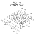
- FIG. 14 shows a conventional light-emitting/receiving device.
- reference numeral 100 denotes a bottomed device case whose inside is divided into two inside portions by a partition board 102.
- Reference numerals 103 and 104 denote lead frames that respectively have supporting portions 103a and 104a at their tips. These lead frames are allowed to pass through a side portion of the device case 100 and are fixed to the device case 100. In more detail, the tip of the lead frame 103 is allowed to enter into one of the two inside portions of the device case 100, while the tip of the lead frame 104 is allowed to enter into the other of the two inside portions of the device case 1.
- Reference numerals 105 and 106 represent lead frames for connection and these lead frames 105 and 106 are allowed to pass through an opposite side portion of the device case 100. Each tip of these lead frames is allowed to enter into the device case 100 and is fixed to the device case 100 so as to oppose one of the tips of the lead frames 103 and 104.
- a light-receiving device 107 is mounted on the supporting portion 103a of the lead frame 103 and a light-emitting device 108 is mounted on the supporting portion 104a of the lead frame 104.
- the light-receiving device 107 is connected to the lead frame 105 through a metallic wire 109 and the light-emitting device 108 is connected to the lead frame 106 through a metallic wire 110.
- a transparent resin material in a liquid state is filled into each of the two inside portions and is hardened.
- This transparent resin material is filled so that its volume becomes smaller than the volume within the device case 100, thereby avoiding its overflow from the device case 100. Then, the transparent resin material is hardened, thereby protecting the light-receiving device 107, the light-emitting device 108, and the metallic wires 109 and 110 within the device case 100.
- the optical semiconductor package described above is produced in a manner such that the rear end side of each of the lead frames 103, 104, 105, and 106 protruding to the outside of the device case 100 is fixed to tie bars 111 and 112, so that a plurality of optical semiconductor packages are produced so as to be connected with each other. Then, the tie bars 111 and 112 are cut and respective optical semiconductor packages are finally obtained, as shown in the drawing.
- the optical semiconductor package described above has the following problems.
- the lead frames 103, 104, 105, and 106 provided for the optical semiconductor package are produced using a method such as etching, so that the price of the optical semiconductor package rises and it is difficult to bring down the price.
- the frames 103, 104, 105, and 106 are delicate, so that it is required to pay close attention to handling of these frames during production work and therefore work efficiency is impaired.
- the mounting of the light-emitting device 108 and the light-receiving device 107 and the connecting of the metallic wires 109 and 110 are machine work but the opening portion of the device case 100 is extremely narrow (around 1.5 mm ⁇ 2 mm, for instance), so that the work range of the machine is limited and therefore the machine work is slowed.
- the liquid resin material having a light transmission property is filled in the device case 100 and is hardened.
- the resin material is filled so that its volume becomes smaller than the volume within the device case 100, thereby avoiding overflow of the resin material from the device case 100 at the time of filling of the resin material.
- the surface shape of each of a light emitting portion and a light incident portion becomes like a concave lens, so that there occurs a problem that the enhancement of device accuracy is hindered by diffusion of light.
- positions of the protrusions of the lead frames 103, 104, 105, and 106 are elevated from the undersurface of the device case 100. Therefore, it is required to form the lead frames 103, 104, 105, and 106 so that these lead frames contact a mounting substrate when the optical semiconductor package is mounted on the mounting substrate. As a result, it is required to spend time and effort.
- the optical semiconductor package uses the device case 100, so that it is difficult to miniaturize the optical semiconductor package.
- the present invention has been made in the light of the aforementioned problems of the optical semiconductor package, and has an object to provide an optical semiconductor package having a laminated structure in which a groove is provided at a position between a light-emitting device and a light-receiving device. Further, in order to enhance a light-shielding property, a resin having a light-shielding property is injected into the groove, or a sheet member having a light-shielding property is inserted into and mounted to the groove.
- the optical semiconductor package constructed in this manner prevents unnecessary rays of light from impinging on a light-receiving surface and exhibits an excellent light-shielding performance without using a specialized device case. Therefore, the present optical semiconductor package is advantageous to miniaturization and makes it easy to perform machine work. Also, unlike the conventional device, the optical semiconductor package according to the present invention does not use high-priced lead frames, so that cost reduction is realized without difficulty and convenience in handling is also achieved. Other objects and constructions of the present invention will become apparent from the following embodiments.
- FIG. 1 is a plan view of an optical semiconductor package of a first embodiment
- FIG. 2 is a side view of the optical semiconductor package.
- reference numeral 11 denotes a printed wiring board.
- This printed wiring board 11 includes a groove DW to be described later at approximately the center thereof, and a circuit pattern having a predetermined shape is formed immediately below the groove DW and on the right and left sides of the groove DW.
- the circuit pattern formed immediately below the groove DW and on the right and left sides of the groove DW is composed of external connection terminals 14a to 14h, electrodes 19a to 19g of a light-receiving device and a light-emitting device, and metallic wires 15a to 15g for connecting the external connection terminals to the electrodes.
- the external connection terminals 14a to 14h described above are also formed on the side surfaces and underside surface of the printed wiring board 11, as shown in FIG. 2.
- the circuit pattern is also provided on the outer surface of the board 11 that coincides with rims of semicircular notches formed on the printed wiring board 11, and is connected to the terminals on the underside surface.
- the light-receiving device 31 having a light-receiving surface 32 is fastened to a portion of the circuit pattern formed on the printed wiring board 11 and the light-emitting device 21 having a light-emitting region 22 is fastened to another portion of the circuit pattern.
- the electrodes 19a to 19f of the light-receiving device 31 are connected to the external connection terminals 14a to 14f through the wires 15a to 15f.
- An unillustrated electrode of the light-emitting device 21 is connected to the external connection terminal 14e and the electrode 19g is connected to the external connection terminal 14g through the wire 15g.
- the light-receiving device 31, the light-emitting device 21, and the wires 15a to 15g described above are protected by a surrounding member 12 formed using a transparent resin material.
- the surrounding member 12 is required to have a height that is equal to or more than the heights of the components of the light-emitting device 21 and the light-receiving device 31 at the minimum, and the thickness of the member 12 is determined by giving attention to the loop heights of the wires 15a to 15g and margins required to bond the optical semiconductor components to the board.
- the surrounding member 12 and a glass substrate 13 are formed on the printed wiring board 11.
- the groove of the present invention is formed so as to have a depth with which direct light from the light-emitting device 21 does not enter the light-receiving device 31 and the circuit pattern of the printed wiring board 11 is not cut. If the circuit pattern does not exist in this portion, there occurs no problem even if the groove depth is set so that the groove reaches the printed wiring board 11.
- the wiring patterns are arranged immediately below the groove. Therefore, the groove is provided so as to have a depth that is somewhat shallower than the total thickness of the surrounding member 12 and the transparent glass substrate 13, as shown in FIG. 2. By setting the groove depth in this manner, there is protected the circuit pattern. As a result, the light-emitting device and the light-receiving device can be connected electrically.
- the groove DW is disposed at the midpoint position between the light-emitting device 21 and the light-receiving device 31 and is a cut-through groove. It is possible to use various methods to produce the groove, although it is required that its cut surface is subjected to mirror-surface finishing if there is used a method such as cutting or grinding.
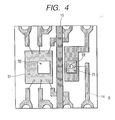
- FIG. 4 shows another form of the groove DW functioning as a light-shielding means.
- the light-shielding means is obtained by pouring a resin 16 having a light-shielding property into the groove portion of the first embodiment.
- FIGS. 5A and 6 are a side view and a perspective view of the second embodiment, respectively.
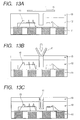
- FIG. 5B A light-shielding sheet member 41 as shown in FIG. 5B can be inserted into and mounted to the groove.
- FIGS. 13A to 13C show the method of inserting the light-shielding sheet member 41. As shown in FIGS. 13A to 13C, the light-shielding sheet member 41 can be readily mounted.
- FIGS. 7 and 8 are an explanatory drawing and a perspective view of a third embodiment, respectively.
- the groove is provided for the third layer and the second layer. In this third embodiment, however, the groove is provided for the printed wiring board 11 (first layer) and the transparent resin layer 12 (second layer).
- the wiring pattern is cut in the manner shown in the drawings, although if it is not required to use the electrodes, it becomes possible to perform groove production from a printed wiring board 11 side like in this embodiment and to shield light by filling the resin 16 having the light-shielding property in the manner shown in FIG. 7. Even in this case, a coating having a light-shielding property may be applied to the machine cut surface of the groove like in the aforementioned example.
- the third layer is made of a glass substrate.
- diffraction gratings 17 are arranged and are used as a reflection-type encoder.
- the diffraction gratings double as optical gratings and the third layer of the package of the present invention, so that it becomes possible to realize a very small reflection-type encoder.
- a phase grating-type Fresnel lens 18 is formed on the top surface of the glass, so that it becomes possible to convert a divergent pencil of rays from the light-emitting device into a parallel pencil of rays and to guide the rays of light to the light-receiving device with efficiency.
- a similar diffraction member 18 is provided also on a light-receiving side, so that there is further enhanced the usage efficiency of light.
- FIG. 11 is a plan view of an optical semiconductor package of the sixth embodiment of the present invention
- FIG. 12 is a side view of an optical semiconductor package of the sixth embodiment of the present invention.
- this printed wiring board 11 similarly to the first embodiment, includes a groove at approximately the center between the light-emitting device 21 and the light-receiving device 31, and a circuit pattern 14 having a predetermined shape is formed immediately below the groove and on the right and left sides of the groove.
- a resin having a light-shielding property is injected into the groove portion so that the direct light from the light-emitting device is shielded certainly.
- the light-receiving device 33 is fastened to the opposite side of the light-receiving device 31 with respect to the light-emitting device 21.
- a groove is provided at approximately the center between the light-emitting device 21 and the light-receiving device 33, a circuit pattern 14 having a predetermined shape is formed immediately below the groove and on the right and left sides of the groove, and a light-shielding resin is injected into groove similarly to the second embodiment.
- the optical semiconductor package of the present invention is of high utility value as a package for a sensor device designed for highly accurate optical measurement.
- the surrounding member 12 described in the aforementioned embodiments is formed using a transparent resin material.
- the material of the surrounding member 12 is not particularly limited to this and a visually opaque material may be used instead so long as the material has a light transmission property with reference to the near-infrared light.
- the transparent glass substrate layer (third layer) with another member that is, for instance, a transparent resin sheet member such as a PET sheet member or a polycarbonate sheet member.
- a transparent resin sheet member such as a PET sheet member or a polycarbonate sheet member.
- the optical semiconductor package according to the present invention has the following advantages.
Landscapes
- Light Receiving Elements (AREA)
- Photo Coupler, Interrupter, Optical-To-Optical Conversion Devices (AREA)
- Led Device Packages (AREA)
Abstract
Description
- The present invention relates to a package for an optical semiconductor in which a light-emitting device and a light-receiving device are placed-within a single package.
- FIG. 14 shows a conventional light-emitting/receiving device. In this drawing,
reference numeral 100 denotes a bottomed device case whose inside is divided into two inside portions by apartition board 102. -
Reference numerals portions device case 100 and are fixed to thedevice case 100. In more detail, the tip of thelead frame 103 is allowed to enter into one of the two inside portions of thedevice case 100, while the tip of thelead frame 104 is allowed to enter into the other of the two inside portions of the device case 1.Reference numerals lead frames device case 100. Each tip of these lead frames is allowed to enter into thedevice case 100 and is fixed to thedevice case 100 so as to oppose one of the tips of thelead frames device 107 is mounted on the supportingportion 103a of thelead frame 103 and a light-emitting device 108 is mounted on the supportingportion 104a of thelead frame 104. The light-receivingdevice 107 is connected to thelead frame 105 through ametallic wire 109 and the light-emitting device 108 is connected to thelead frame 106 through ametallic wire 110. - In the
device case 100 described above, a transparent resin material in a liquid state is filled into each of the two inside portions and is hardened. This transparent resin material is filled so that its volume becomes smaller than the volume within thedevice case 100, thereby avoiding its overflow from thedevice case 100. Then, the transparent resin material is hardened, thereby protecting the light-receivingdevice 107, the light-emitting device 108, and themetallic wires device case 100. - The optical semiconductor package described above is produced in a manner such that the rear end side of each of the
lead frames device case 100 is fixed totie bars tie bars - The optical semiconductor package described above has the following problems. First, the
lead frames frames - Also, the mounting of the light-
emitting device 108 and the light-receivingdevice 107 and the connecting of themetallic wires device case 100 is extremely narrow (around 1.5 mm × 2 mm, for instance), so that the work range of the machine is limited and therefore the machine work is slowed. - The liquid resin material having a light transmission property is filled in the
device case 100 and is hardened. When doing so, the resin material is filled so that its volume becomes smaller than the volume within thedevice case 100, thereby avoiding overflow of the resin material from thedevice case 100 at the time of filling of the resin material. In this case, however, the surface shape of each of a light emitting portion and a light incident portion becomes like a concave lens, so that there occurs a problem that the enhancement of device accuracy is hindered by diffusion of light. - Further, positions of the protrusions of the
lead frames device case 100. Therefore, it is required to form thelead frames device case 100, so that it is difficult to miniaturize the optical semiconductor package. - The present invention has been made in the light of the aforementioned problems of the optical semiconductor package, and has an object to provide an optical semiconductor package having a laminated structure in which a groove is provided at a position between a light-emitting device and a light-receiving device. Further, in order to enhance a light-shielding property, a resin having a light-shielding property is injected into the groove, or a sheet member having a light-shielding property is inserted into and mounted to the groove.
- The optical semiconductor package constructed in this manner prevents unnecessary rays of light from impinging on a light-receiving surface and exhibits an excellent light-shielding performance without using a specialized device case. Therefore, the present optical semiconductor package is advantageous to miniaturization and makes it easy to perform machine work. Also, unlike the conventional device, the optical semiconductor package according to the present invention does not use high-priced lead frames, so that cost reduction is realized without difficulty and convenience in handling is also achieved. Other objects and constructions of the present invention will become apparent from the following embodiments.
-
- FIG. 1 is a plan view of an optical semiconductor package showing a first embodiment of the present invention;
- FIG. 2 is a side view of the optical semiconductor package;
- FIG. 3 is a perspective view of a light-shielding groove provided for the optical semiconductor package;
- FIG. 4 is a plan view of an optical semiconductor package showing a second embodiment of the present invention;
- FIG. 5A is a side view of the optical semiconductor package;
- FIG. 5B is a side view of a modified example of the optical semiconductor package;
- FIG. 6 is a perspective view of a light-shielding groove provided for the optical semiconductor package;
- FIG. 7 is a side view of an optical semiconductor package showing a third embodiment of the present invention;
- FIG. 8 is a perspective view of a light-shielding groove provided for the optical semiconductor package;
- FIG. 9 is a perspective view of an optical semiconductor package showing a fourth embodiment of the present invention;
- FIG. 10 is a perspective view of an optical semiconductor package showing a fifth embodiment of the present invention;
- FIG. 11 is a plan view of an optical semiconductor package showing a sixth embodiment of the present invention;
- FIG. 12 is a side view of an optical semiconductor package showing a sixth embodiment of the present invention;
- FIGS. 13A, 13B and 13C are a side view of an optical semiconductor package showing the insertion method of a sheet member having a light-shielding property in a modified example of a second embodiment of the present invention; and
- FIG. 14 is a perspective view of a conventional optical semiconductor package.
-
- Now, embodiments of the present invention will be described with reference to the accompanying drawings. FIG. 1 is a plan view of an optical semiconductor package of a first embodiment, while FIG. 2 is a side view of the optical semiconductor package. In these drawings,
reference numeral 11 denotes a printed wiring board. This printedwiring board 11 includes a groove DW to be described later at approximately the center thereof, and a circuit pattern having a predetermined shape is formed immediately below the groove DW and on the right and left sides of the groove DW. - In FIG. 1, the circuit pattern formed immediately below the groove DW and on the right and left sides of the groove DW is composed of
external connection terminals 14a to 14h,electrodes 19a to 19g of a light-receiving device and a light-emitting device, andmetallic wires 15a to 15g for connecting the external connection terminals to the electrodes. - The
external connection terminals 14a to 14h described above are also formed on the side surfaces and underside surface of the printedwiring board 11, as shown in FIG. 2. The circuit pattern is also provided on the outer surface of theboard 11 that coincides with rims of semicircular notches formed on the printedwiring board 11, and is connected to the terminals on the underside surface. - The light-receiving
device 31 having a light-receivingsurface 32 is fastened to a portion of the circuit pattern formed on the printedwiring board 11 and the light-emitting device 21 having a light-emittingregion 22 is fastened to another portion of the circuit pattern. Also, theelectrodes 19a to 19f of the light-receivingdevice 31 are connected to theexternal connection terminals 14a to 14f through thewires 15a to 15f. An unillustrated electrode of the light-emitting device 21 is connected to theexternal connection terminal 14e and theelectrode 19g is connected to theexternal connection terminal 14g through the wire 15g. - The light-receiving
device 31, the light-emittingdevice 21, and thewires 15a to 15g described above are protected by a surroundingmember 12 formed using a transparent resin material. As is apparent from FIG. 2, the surroundingmember 12 is required to have a height that is equal to or more than the heights of the components of the light-emittingdevice 21 and the light-receivingdevice 31 at the minimum, and the thickness of themember 12 is determined by giving attention to the loop heights of thewires 15a to 15g and margins required to bond the optical semiconductor components to the board. - The surrounding
member 12 and aglass substrate 13 are formed on the printedwiring board 11. The groove of the present invention is formed so as to have a depth with which direct light from the light-emittingdevice 21 does not enter the light-receivingdevice 31 and the circuit pattern of the printedwiring board 11 is not cut. If the circuit pattern does not exist in this portion, there occurs no problem even if the groove depth is set so that the groove reaches the printedwiring board 11. - In this embodiment, as shown in FIG. 1, the wiring patterns are arranged immediately below the groove. Therefore, the groove is provided so as to have a depth that is somewhat shallower than the total thickness of the surrounding
member 12 and thetransparent glass substrate 13, as shown in FIG. 2. By setting the groove depth in this manner, there is protected the circuit pattern. As a result, the light-emitting device and the light-receiving device can be connected electrically. - As can been from the perspective view shown in FIG. 3, the groove DW is disposed at the midpoint position between the light-emitting
device 21 and the light-receivingdevice 31 and is a cut-through groove. It is possible to use various methods to produce the groove, although it is required that its cut surface is subjected to mirror-surface finishing if there is used a method such as cutting or grinding. - As a result of the mirror-surface finishing, rays of light are emitted from the light-emitting device so that there is reduced diffused component light of rays of light from the inside of the machine cut surface of the resin substrate and the glass substrate. Therefore, noise light hardly enters into the light-receiving device and there is realized a sufficient light-shielding performance. Note that in the case where the cut surface is a diffusing surface from an optical viewpoint, considerable rays of light enter the light-receiving portion, so that there occurs reduction in the light-shielding performance.
- For this reason, in the second embodiment to be described next, there will be explained a construction where it is not required to perform the mirror-surface finishing on the machine cut surface and the light-shielding function of the present invention is sufficiently attained even if the mirror-surface finishing is not performed.
- FIG. 4 shows another form of the groove DW functioning as a light-shielding means. In this drawing, the light-shielding means is obtained by pouring a
resin 16 having a light-shielding property into the groove portion of the first embodiment. - With this method, a high light-shielding performance is obtained at all times irrespective of the degree of finishing of the groove in the aforementioned first embodiment. Although the
resin 16 having the light-shielding property becomes necessary, a reliable light-shielding means is obtained and a high substantial economical effect is achieved. - FIGS. 5A and 6 are a side view and a perspective view of the second embodiment, respectively.
- Here, it is not necessarily required to fill the groove with a light-shielding material in the manner shown in FIG. 4. That is, as a modification of this embodiment, it is possible to apply a coating having a light-shielding property to the machine cut surface of the groove. A light-shielding
sheet member 41 as shown in FIG. 5B can be inserted into and mounted to the groove. FIGS. 13A to 13C show the method of inserting the light-shieldingsheet member 41. As shown in FIGS. 13A to 13C, the light-shieldingsheet member 41 can be readily mounted. - FIGS. 7 and 8 are an explanatory drawing and a perspective view of a third embodiment, respectively.
- In the first and second embodiments, the groove is provided for the third layer and the second layer. In this third embodiment, however, the groove is provided for the printed wiring board 11 (first layer) and the transparent resin layer 12 (second layer).
- In this embodiment, the wiring pattern is cut in the manner shown in the drawings, although if it is not required to use the electrodes, it becomes possible to perform groove production from a printed
wiring board 11 side like in this embodiment and to shield light by filling theresin 16 having the light-shielding property in the manner shown in FIG. 7. Even in this case, a coating having a light-shielding property may be applied to the machine cut surface of the groove like in the aforementioned example. - In the optical semiconductor package of the present invention, the third layer is made of a glass substrate.
- It is possible to mount various optical means on this
substrate 13. In FIG. 9,diffraction gratings 17 are arranged and are used as a reflection-type encoder. The diffraction gratings double as optical gratings and the third layer of the package of the present invention, so that it becomes possible to realize a very small reflection-type encoder. - In a like manner as in the fourth embodiment, in FIG. 10, a phase grating-
type Fresnel lens 18 is formed on the top surface of the glass, so that it becomes possible to convert a divergent pencil of rays from the light-emitting device into a parallel pencil of rays and to guide the rays of light to the light-receiving device with efficiency. - Needless to say, a
similar diffraction member 18 is provided also on a light-receiving side, so that there is further enhanced the usage efficiency of light. - Although, in the first embodiment, each one of the light-emitting device and the light-receiving device is mounted on this substrate, in this sixth embodiment, a single light-emitting device is mounted and two light-receiving devices are mounted. FIG. 11 is a plan view of an optical semiconductor package of the sixth embodiment of the present invention, and FIG. 12 is a side view of an optical semiconductor package of the sixth embodiment of the present invention. In these drawings, similarly to the first embodiment, this printed
wiring board 11 includes a groove at approximately the center between the light-emittingdevice 21 and the light-receivingdevice 31, and acircuit pattern 14 having a predetermined shape is formed immediately below the groove and on the right and left sides of the groove. Similarly to the second embodiment, a resin having a light-shielding property is injected into the groove portion so that the direct light from the light-emitting device is shielded certainly. Further, in this embodiment, the light-receivingdevice 33 is fastened to the opposite side of the light-receivingdevice 31 with respect to the light-emittingdevice 21. In order not to guide the direct light from the light-emittingdevice 21 to the light-receivingdevice 33, a groove is provided at approximately the center between the light-emittingdevice 21 and the light-receivingdevice 33, acircuit pattern 14 having a predetermined shape is formed immediately below the groove and on the right and left sides of the groove, and a light-shielding resin is injected into groove similarly to the second embodiment. - In this embodiment, there is no restriction in the number of the light-emitting devices and the light-receiving devices fastened on this printed
wiring board 11. - As described above, with the construction of the present invention, there is provided a light-shielding means having a high light-shielding performance. In addition, the third layer is a transparent glass substrate, so that it is possible to obtain high flatness. Therefore, in the case where a coherent light source, such as a semiconductor laser, a surface emitting laser, or a point light source LED having a current bottleneck structure, is mounted as the light-emitting device, for instance, it is possible to emit light to the outside of the optical semiconductor package without causing any deleterious effect on the surface accuracy of the light emitting wave surface. In a like manner, also on the light-receiving surface side, it becomes possible to perform light reception while suppressing distortion of the wave surface of the light wave as much as possible. Accordingly, in particular, the optical semiconductor package of the present invention is of high utility value as a package for a sensor device designed for highly accurate optical measurement.
- In a like manner, in the case where a fine-pitch light-receiving device array is used on the light-receiving device surface, for instance, if the flatness of the third layer is low, desired rays of light do not enter each light-receiving area of the light-receiving device array and therefore there is incurred performance degradation. With the present invention, however, the performance is substantially improved.
- In particular, in the case of a circuit pattern construction where a circuit on the light-emitting device side and a circuit on the light-receiving device side are connected to each other, it has been difficult to use a light-shielding means, which completely divides the area of a light-emitting device from the area of a light-receiving device, on the layout surface of the circuit pattern. With the light-shielding means of the present invention, however, there is obtained an advantage that it becomes possible to establish connection of the circuit pattern between the light-emitting device side and the light-receiving device side without cutting the circuit pattern.
- Also, the surrounding
member 12 described in the aforementioned embodiments is formed using a transparent resin material. In the case where the emission light of the light-emittingdevice 21 is near-infrared light, however, the material of the surroundingmember 12 is not particularly limited to this and a visually opaque material may be used instead so long as the material has a light transmission property with reference to the near-infrared light. - It is possible to replace the transparent glass substrate layer (third layer) with another member that is, for instance, a transparent resin sheet member such as a PET sheet member or a polycarbonate sheet member.
- The optical semiconductor package according to the present invention has the following advantages.
- (1) It is not required to use high-priced components such as the lead frames 3, 4, 5, and 6, so that there is reduced product cost.
- (2) The device case 1 becomes unnecessary, so that there is reduced the size of the device in comparison with the conventional product.
- (3) It is possible to form the light incident portion and the light emitting portion so as to have a shape achieving a high optical effect, so that there is enhanced device accuracy.
- (4) The mounting of the light-emitting
device 21 and the light-receivingdevice 31, the connecting of thewire 15, and the like are performed in a wide space, so that the work range of a work machine is not limited and therefore there is improved productivity. - (5) The groove DW is not formed on the circuit pattern, so that it becomes possible to make connection of the circuit pattern across the light-shielding member. As a result, there is increased flexibility in designing and there is obtained an advantage also from the viewpoint of miniaturization designing.
-
Claims (10)
- A package for an optical semiconductor comprising :wherein a groove is provided for the surrounding member layer between the light-emitting device and the light-receiving device.a wiring board on which a light-emitting device and a light-receiving device are mounted; anda surrounding member layer made of a resin material having a light transmittance property so as to cover outer surfaces of the light-emitting device and the light-receiving device,
- A package for an optical semiconductor according to claim 1,
wherein a material having a light-shielding property is provided in the groove. - A package for an optical semiconductor according to claim 1 or claim 2,
wherein a glass substrate layer having a light transmittance property is provided on the surrounding member layer. - A package for an optical semiconductor according to claim 3,
wherein the glass substrate layer is a light diffraction member. - A package for an optical semiconductor according to claim 2,
wherein a sheet member having a light-shielding property is inserted into the groove. - A package for an optical semiconductor according to any preceding claim,
wherein the light-emitting device and the light-receiving device are connected electrically on the wiring board. - An optical semiconductor assembly comprising:characterised by a groove in the surrounding member between the or each light-emitting device and the or each light-receiving device.a wiring board;at least one light-emitting device mounted on said wiring board;at least one light-receiving device mounted on said wiring board;a surrounding member of a material having a light transmittance property covering said light-emitting and light-receiving devices;
- An assembly according to claim 7 wherein the surrounding member is a transparent resin.
- An assembly according to claim 7 or claim 8 further comprising a substrate layer on the surrounding member.
- An assembly according to any one of claims 7 to 9 wherein light-shielding means is provided in said groove.
Applications Claiming Priority (4)
| Application Number | Priority Date | Filing Date | Title |
|---|---|---|---|
| JP2002103628 | 2002-04-05 | ||
| JP2002103628 | 2002-04-05 | ||
| JP2003085357 | 2003-03-26 | ||
| JP2003085357A JP2004006753A (en) | 2002-04-05 | 2003-03-26 | Optical semiconductor package |
Publications (3)
| Publication Number | Publication Date |
|---|---|
| EP1351319A2 true EP1351319A2 (en) | 2003-10-08 |
| EP1351319A3 EP1351319A3 (en) | 2009-04-15 |
| EP1351319B1 EP1351319B1 (en) | 2014-04-30 |
Family
ID=28043873
Family Applications (1)
| Application Number | Title | Priority Date | Filing Date |
|---|---|---|---|
| EP03252143.7A Expired - Lifetime EP1351319B1 (en) | 2002-04-05 | 2003-04-04 | Package for optical semiconductor |
Country Status (3)
| Country | Link |
|---|---|
| US (1) | US7026654B2 (en) |
| EP (1) | EP1351319B1 (en) |
| JP (1) | JP2004006753A (en) |
Cited By (10)
| Publication number | Priority date | Publication date | Assignee | Title |
|---|---|---|---|---|
| DE102007009531A1 (en) * | 2007-02-27 | 2008-08-28 | Osram Opto Semiconductors Gmbh | Jet device manufacturing method, involves separating common casting bodies and common separation body in carrier body, and arranging transmission units, receiving units, transparent casting bodies and opaque separation body on carrier body |
| GB2486000A (en) * | 2010-11-30 | 2012-06-06 | St Microelectronics Res & Dev | Optical proximity detectors with arrangements for reducing internal light propagation from emitter to detector |
| US8461533B2 (en) | 2010-11-25 | 2013-06-11 | Stmicroelectronics (Research & Development) Ltd | Radiation sensor |
| US8552379B2 (en) | 2010-11-25 | 2013-10-08 | Stmicroelectronics (Research & Development) Limited | Radiation sensor |
| US8748856B2 (en) | 2010-11-30 | 2014-06-10 | Stmicroelectronics (Research & Development) Limited | Compact proximity sensor suppressing internal reflection |
| CN104009030A (en) * | 2013-02-20 | 2014-08-27 | 马克西姆综合产品公司 | Multichip wafer level package (WLP) optical device |
| US9006636B2 (en) | 2010-11-30 | 2015-04-14 | Stmicroelectronics (Research & Development) Limited | Radiation sensor |
| CN106024649A (en) * | 2016-07-12 | 2016-10-12 | 希睿(厦门)科技有限公司 | Ultra-thin ambient light and proximity sensor wafer level package and package method thereof |
| CN106469660A (en) * | 2015-08-21 | 2017-03-01 | 意法半导体(R&D)有限公司 | Molded Range and Proximity Sensors with Optical Resin Lens |
| CN107799512A (en) * | 2017-11-28 | 2018-03-13 | 无锡豪帮高科股份有限公司 | A kind of three-dimensional encapsulation integrates the structure and its method of photoelectric coupled circuit |
Families Citing this family (45)
| Publication number | Priority date | Publication date | Assignee | Title |
|---|---|---|---|---|
| DE112004002472T5 (en) * | 2003-12-17 | 2008-08-28 | Sumitomo Chemical Co. Ltd. | Organic device for light-light conversion |
| JP2006038572A (en) * | 2004-07-26 | 2006-02-09 | Sharp Corp | Reflective encoder and electronic apparatus using the reflective encoder |
| JP2006261302A (en) * | 2005-03-16 | 2006-09-28 | Rohm Co Ltd | Optical communication module |
| JP4803641B2 (en) * | 2005-05-12 | 2011-10-26 | オリンパス株式会社 | Optical encoder |
| JP5038623B2 (en) * | 2005-12-27 | 2012-10-03 | 株式会社東芝 | Optical semiconductor device and manufacturing method thereof |
| JP2008028025A (en) * | 2006-07-19 | 2008-02-07 | Canon Inc | Reflective sensor |
| KR100820627B1 (en) * | 2006-07-31 | 2008-04-10 | 한국 고덴시 주식회사 | Reflective optical sensor package and its manufacturing method |
| WO2008126836A1 (en) | 2007-04-10 | 2008-10-23 | Olympus Corporation | Optical type encoder |
| US8574944B2 (en) * | 2008-03-28 | 2013-11-05 | The University Of Toledo | System for selectively filling pin holes, weak shunts and/or scribe lines in photovoltaic devices and photovoltaic cells made thereby |
| TWM363080U (en) * | 2009-01-21 | 2009-08-11 | Pixart Imaging Inc | Packaging structure |
| US8232541B2 (en) * | 2009-04-14 | 2012-07-31 | Intersil Americas Inc. | Optical sensors that reduce specular reflections |
| US8324602B2 (en) * | 2009-04-14 | 2012-12-04 | Intersil Americas Inc. | Optical sensors that reduce specular reflections |
| US8804368B2 (en) * | 2009-04-30 | 2014-08-12 | Sony Corporation | Downward-facing optical component module |
| US8362515B2 (en) * | 2010-04-07 | 2013-01-29 | Chia-Ming Cheng | Chip package and method for forming the same |
| DE102010054781B4 (en) * | 2010-12-16 | 2014-09-11 | Epcos Ag | Module for reducing thermo-mechanical stress and method for its production |
| US9130109B2 (en) | 2011-01-20 | 2015-09-08 | Rohm Co., Ltd. | Optical apparatus |
| JP5610156B2 (en) * | 2011-01-31 | 2014-10-22 | 日立金属株式会社 | Photoelectric conversion module and method for manufacturing photoelectric conversion module |
| US20120223231A1 (en) * | 2011-03-01 | 2012-09-06 | Lite-On Singapore Pte. Ltd. | Proximity sensor having electro-less plated shielding structure |
| JP5743075B2 (en) * | 2011-03-31 | 2015-07-01 | セイコーインスツル株式会社 | Optical sensor and optical sensor manufacturing method |
| US8677605B2 (en) * | 2011-07-22 | 2014-03-25 | Lite-On Singapore Pte. Ltd. | Method for manufacturing sensor unit |
| CN103747723B (en) * | 2011-08-19 | 2015-11-25 | 株式会社村田制作所 | biological sensor |
| EP3053519B1 (en) * | 2011-08-19 | 2023-08-16 | Murata Manufacturing Co., Ltd. | Biosensor |
| TWM428490U (en) * | 2011-09-27 | 2012-05-01 | Lingsen Precision Ind Ltd | Optical module packaging unit |
| JP2013197302A (en) | 2012-03-19 | 2013-09-30 | Toshiba Corp | Semiconductor device and manufacturing method therefor |
| JP6077528B2 (en) * | 2012-04-25 | 2017-02-08 | 京セラ株式会社 | Light emitting / receiving element module and sensor device using the same |
| US9570648B2 (en) | 2012-06-15 | 2017-02-14 | Intersil Americas LLC | Wafer level optical proximity sensors and systems including wafer level optical proximity sensors |
| US20140003637A1 (en) * | 2012-06-28 | 2014-01-02 | Starkey Laboratories, Inc. | Infrared sensors for hearing assistance devices |
| JP2013070078A (en) * | 2012-11-21 | 2013-04-18 | Canon Inc | Reflection type sensor |
| TWI527166B (en) * | 2013-07-25 | 2016-03-21 | 菱生精密工業股份有限公司 | The package structure of the optical module |
| US9496247B2 (en) * | 2013-08-26 | 2016-11-15 | Optiz, Inc. | Integrated camera module and method of making same |
| US9711552B2 (en) * | 2014-08-19 | 2017-07-18 | Heptagon Micro Optics Pte. Ltd. | Optoelectronic modules having a silicon substrate, and fabrication methods for such modules |
| US9721837B2 (en) | 2015-04-16 | 2017-08-01 | Intersil Americas LLC | Wafer level optoelectronic device packages with crosstalk barriers and methods for making the same |
| JP6445940B2 (en) * | 2015-08-03 | 2018-12-26 | 株式会社東芝 | Optical coupling device |
| CN107785357B (en) * | 2016-08-26 | 2025-04-08 | 意法半导体研发(深圳)有限公司 | Anti-adhesive overflow cap for optical sensor package |
| JP6946921B2 (en) * | 2017-10-17 | 2021-10-13 | 株式会社デンソー | Housing of light emitting / receiving device |
| US10921447B2 (en) * | 2018-01-29 | 2021-02-16 | Rohm Co., Ltd. | Control circuit of light emitting and receiving device |
| CN110392820B (en) * | 2018-02-20 | 2020-05-01 | 三菱电机株式会社 | absolute encoder |
| CN110556368B (en) * | 2018-06-04 | 2021-03-23 | 艾普柯微电子(上海)有限公司 | Photoelectric sensor and preparation method thereof |
| US20200150270A1 (en) * | 2018-11-14 | 2020-05-14 | Lite-On Singapore Pte. Ltd. | Infrared proximity sensor |
| US12000959B2 (en) * | 2018-11-14 | 2024-06-04 | Lite-On Singapore Pte. Ltd. | Proximity sensor and electronic device having the same |
| US11837686B2 (en) * | 2018-12-07 | 2023-12-05 | Advanced Semiconductor Engineering, Inc. | Optical device package and method for manufacturing the same |
| JP7206489B2 (en) * | 2019-03-07 | 2023-01-18 | ミツミ電機株式会社 | Optical module and optical encoder |
| EP4000921A4 (en) * | 2019-07-16 | 2023-07-12 | Agc Inc. | TRANSPARENT SENSING DEVICE, LAMINATED GLASS AND METHOD OF MAKING A TRANSPARENT SENSING DEVICE |
| JP2021029377A (en) | 2019-08-19 | 2021-03-01 | カシオ計算機株式会社 | Window members, window member manufacturing methods, and electronic devices |
| CN113900110B (en) * | 2020-06-22 | 2025-09-02 | 光宝科技新加坡私人有限公司 | Optical sensing device |
Citations (1)
| Publication number | Priority date | Publication date | Assignee | Title |
|---|---|---|---|---|
| EP0216935B1 (en) | 1985-03-08 | 1991-02-20 | Olympus Optical Co., Ltd. | Solid-state image pickup device and method of manufacturing the same |
Family Cites Families (35)
| Publication number | Priority date | Publication date | Assignee | Title |
|---|---|---|---|---|
| JPS5717187A (en) * | 1980-07-07 | 1982-01-28 | Toshiba Corp | Manufacture of semiconductor device for detecting light |
| US4565924A (en) * | 1982-03-05 | 1986-01-21 | Omron Tateisi Electronics Co. | Light signal binary device with optical feedback |
| JPS5986272A (en) * | 1982-11-09 | 1984-05-18 | Toshiba Corp | Manufacture of photodetecting semiconductor device |
| JPS6046555B2 (en) * | 1984-06-26 | 1985-10-16 | 松下電器産業株式会社 | Photocoupler |
| JP2778054B2 (en) * | 1988-10-27 | 1998-07-23 | 日本電気株式会社 | Resin-sealed photo interrupter |
| US5873821A (en) * | 1992-05-18 | 1999-02-23 | Non-Invasive Technology, Inc. | Lateralization spectrophotometer |
| JPH02154475A (en) * | 1988-12-06 | 1990-06-13 | Nec Corp | Manufacture of photodetector |
| JPH03142939A (en) * | 1989-10-30 | 1991-06-18 | Fuji Electric Co Ltd | Method and metallic mold for molding plastic molded type semiconductor element |
| JP2530369Y2 (en) * | 1990-10-05 | 1997-03-26 | シャープ株式会社 | Optical coupling device |
| KR940007588B1 (en) * | 1990-11-13 | 1994-08-20 | 가부시키가이샤 도시바 | Semiconductor opto-electro transducer |
| US5291038A (en) * | 1990-12-19 | 1994-03-01 | Sharp Kabushiki Kaisha | Reflective type photointerrupter |
| JP2534358Y2 (en) * | 1991-01-10 | 1997-04-30 | シャープ株式会社 | Transmission type optical coupling device |
| US5233177A (en) * | 1991-01-18 | 1993-08-03 | The Furukawa Electric Co., Ltd. | Optical sensor with fiberless optical member |
| JP3009379U (en) * | 1994-08-05 | 1995-04-04 | 船井電機株式会社 | Reel sensor |
| JPH08125210A (en) * | 1994-10-24 | 1996-05-17 | Jiyousuke Nakada | Light receiving element, light receiving element array, and electrolysis apparatus using the same |
| US20020053742A1 (en) * | 1995-09-01 | 2002-05-09 | Fumio Hata | IC package and its assembly method |
| US6011254A (en) * | 1995-09-21 | 2000-01-04 | Rohm Co., Ltd. | Photoelectric tilt-detecting sensor and method of fabricating the same |
| IL120464A (en) * | 1997-03-17 | 2000-01-31 | Phone Or Ltd | Sensor and method for measuring distances to and/or physical properties of a medium |
| JPH11261493A (en) * | 1998-03-13 | 1999-09-24 | Hosiden Corp | Optical element |
| JPH11289105A (en) * | 1998-04-03 | 1999-10-19 | Citizen Electronics Co Ltd | Photoreflector and method of manufacturing the same |
| JP2000069595A (en) * | 1998-08-19 | 2000-03-03 | Nippon Ceramic Co Ltd | Optical microphone |
| JP3590729B2 (en) * | 1998-11-10 | 2004-11-17 | シャープ株式会社 | Optical coupling device |
| JP4246855B2 (en) * | 1999-07-06 | 2009-04-02 | シチズン電子株式会社 | Reflective optical sensor and manufacturing method thereof |
| JP3676136B2 (en) * | 1999-08-23 | 2005-07-27 | シャープ株式会社 | Optical coupling element |
| US6625036B1 (en) * | 1999-08-31 | 2003-09-23 | Rohm Co., Ltd. | Infrared data communication module and method of making the same |
| JP3585216B2 (en) * | 2000-04-04 | 2004-11-04 | シャープ株式会社 | Reflection type photo interrupter |
| JP2001332799A (en) * | 2000-05-19 | 2001-11-30 | Rohm Co Ltd | Molded semiconductor laser |
| JP2001339574A (en) * | 2000-05-29 | 2001-12-07 | Rohm Co Ltd | Image reader |
| JP2002176202A (en) * | 2000-12-11 | 2002-06-21 | Rohm Co Ltd | Optical device, photo interrupter having the same, and method of manufacturing optical device |
| JP2003008141A (en) * | 2001-06-26 | 2003-01-10 | Sumitomo Electric Ind Ltd | Light emitting device, optical module, and fiber stub component |
| US6633030B2 (en) * | 2001-08-31 | 2003-10-14 | Fiarchild Semiconductor | Surface mountable optocoupler package |
| JP4750983B2 (en) * | 2001-09-21 | 2011-08-17 | シチズン電子株式会社 | Bi-directional optical transmission device |
| JP3797915B2 (en) * | 2001-10-25 | 2006-07-19 | シチズン電子株式会社 | Bi-directional optical transmission device |
| US6740862B2 (en) * | 2002-03-13 | 2004-05-25 | Phone-Or Ltd. | Optical transducers and methods of making same |
| US6822750B2 (en) * | 2002-03-13 | 2004-11-23 | Phone-Or Ltd. | Optical transducers and methods of making same |
-
2003
- 2003-03-26 JP JP2003085357A patent/JP2004006753A/en active Pending
- 2003-04-03 US US10/406,943 patent/US7026654B2/en not_active Expired - Fee Related
- 2003-04-04 EP EP03252143.7A patent/EP1351319B1/en not_active Expired - Lifetime
Patent Citations (1)
| Publication number | Priority date | Publication date | Assignee | Title |
|---|---|---|---|---|
| EP0216935B1 (en) | 1985-03-08 | 1991-02-20 | Olympus Optical Co., Ltd. | Solid-state image pickup device and method of manufacturing the same |
Cited By (15)
| Publication number | Priority date | Publication date | Assignee | Title |
|---|---|---|---|---|
| DE102007009531A1 (en) * | 2007-02-27 | 2008-08-28 | Osram Opto Semiconductors Gmbh | Jet device manufacturing method, involves separating common casting bodies and common separation body in carrier body, and arranging transmission units, receiving units, transparent casting bodies and opaque separation body on carrier body |
| US8552379B2 (en) | 2010-11-25 | 2013-10-08 | Stmicroelectronics (Research & Development) Limited | Radiation sensor |
| US8461533B2 (en) | 2010-11-25 | 2013-06-11 | Stmicroelectronics (Research & Development) Ltd | Radiation sensor |
| US8928893B2 (en) | 2010-11-30 | 2015-01-06 | Stmicroelectronics (Research & Development) Limited | Proximity sensor |
| US8748856B2 (en) | 2010-11-30 | 2014-06-10 | Stmicroelectronics (Research & Development) Limited | Compact proximity sensor suppressing internal reflection |
| GB2486000A (en) * | 2010-11-30 | 2012-06-06 | St Microelectronics Res & Dev | Optical proximity detectors with arrangements for reducing internal light propagation from emitter to detector |
| US9006636B2 (en) | 2010-11-30 | 2015-04-14 | Stmicroelectronics (Research & Development) Limited | Radiation sensor |
| CN104009030A (en) * | 2013-02-20 | 2014-08-27 | 马克西姆综合产品公司 | Multichip wafer level package (WLP) optical device |
| CN106469660A (en) * | 2015-08-21 | 2017-03-01 | 意法半导体(R&D)有限公司 | Molded Range and Proximity Sensors with Optical Resin Lens |
| US10684389B2 (en) | 2015-08-21 | 2020-06-16 | Stmicroelectronics (Research & Development) Limited | Molded range and proximity sensor with optical resin lens |
| CN113161318A (en) * | 2015-08-21 | 2021-07-23 | 意法半导体(R&D)有限公司 | Sensor package |
| US11137517B2 (en) | 2015-08-21 | 2021-10-05 | Stmicroelectronics (Research & Development) Limited | Molded range and proximity sensor with optical resin lens |
| US11693149B2 (en) | 2015-08-21 | 2023-07-04 | Stmicroelectronics (Research & Development) Limited | Molded range and proximity sensor with optical resin lens |
| CN106024649A (en) * | 2016-07-12 | 2016-10-12 | 希睿(厦门)科技有限公司 | Ultra-thin ambient light and proximity sensor wafer level package and package method thereof |
| CN107799512A (en) * | 2017-11-28 | 2018-03-13 | 无锡豪帮高科股份有限公司 | A kind of three-dimensional encapsulation integrates the structure and its method of photoelectric coupled circuit |
Also Published As
| Publication number | Publication date |
|---|---|
| EP1351319B1 (en) | 2014-04-30 |
| US20030189213A1 (en) | 2003-10-09 |
| EP1351319A3 (en) | 2009-04-15 |
| JP2004006753A (en) | 2004-01-08 |
| US7026654B2 (en) | 2006-04-11 |
Similar Documents
| Publication | Publication Date | Title |
|---|---|---|
| US7026654B2 (en) | Package for optical semiconductor | |
| KR101389719B1 (en) | Semiconductor light-emitting device | |
| US9054279B2 (en) | Optoelectronic component disposed in a recess of a housing and electrical componenet disposed in the housing | |
| JP3930710B2 (en) | Chip-type light emitting diode and manufacturing method thereof | |
| JP3644927B2 (en) | Surface emitting device | |
| JP5261320B2 (en) | Optical distance measuring sensor and electronic device equipped with the same | |
| KR20080070067A (en) | Semiconductor package, manufacturing method, semiconductor module, and electronic device | |
| US7193299B2 (en) | Conductor frame and housing for a radiation-emitting component, radiation-emitting component and display and/or illumination system using radiation-emitting components | |
| TWI447612B (en) | Photovoltaic module having at least one photoreceptor circuit | |
| US7453079B2 (en) | Surface mount type photo-interrupter and method for manufacturing the same | |
| JP2015060998A (en) | Sensor module and three-dimentional wiring circuit board used in the same | |
| JP4172558B2 (en) | Infrared communication device | |
| JPH1124608A (en) | LED display | |
| JP3900606B2 (en) | Infrared data communication module | |
| CN116266562A (en) | Optical sensing module and packaging method thereof | |
| CN102460862B (en) | Optical communication module | |
| JP2023547258A (en) | Package structure and electronic equipment | |
| KR102114708B1 (en) | Optical sensor package | |
| JP2009094935A (en) | Image sensor module | |
| JP2003008072A (en) | Light emitting diode | |
| KR102114699B1 (en) | Optical sensor package | |
| JP2002252357A (en) | Photoelectric sensor | |
| KR100821222B1 (en) | Rod-shaped LED Package and Manufacturing Method Thereof | |
| JPS62133774A (en) | Photosensor | |
| JP2022168760A (en) | Light emitting device, electrical equipment, and substrate for light emitting device |
Legal Events
| Date | Code | Title | Description |
|---|---|---|---|
| PUAI | Public reference made under article 153(3) epc to a published international application that has entered the european phase |
Free format text: ORIGINAL CODE: 0009012 |
|
| AK | Designated contracting states |
Kind code of ref document: A2 Designated state(s): AT BE BG CH CY CZ DE DK EE ES FI FR GB GR HU IE IT LI LU MC NL PT RO SE SI SK TR |
|
| AX | Request for extension of the european patent |
Extension state: AL LT LV MK |
|
| PUAL | Search report despatched |
Free format text: ORIGINAL CODE: 0009013 |
|
| AK | Designated contracting states |
Kind code of ref document: A3 Designated state(s): AT BE BG CH CY CZ DE DK EE ES FI FR GB GR HU IE IT LI LU MC NL PT RO SE SI SK TR |
|
| AX | Request for extension of the european patent |
Extension state: AL LT LV MK |
|
| 17P | Request for examination filed |
Effective date: 20091015 |
|
| 17Q | First examination report despatched |
Effective date: 20091106 |
|
| AKX | Designation fees paid |
Designated state(s): DE FR GB |
|
| GRAP | Despatch of communication of intention to grant a patent |
Free format text: ORIGINAL CODE: EPIDOSNIGR1 |
|
| INTG | Intention to grant announced |
Effective date: 20131107 |
|
| GRAS | Grant fee paid |
Free format text: ORIGINAL CODE: EPIDOSNIGR3 |
|
| GRAA | (expected) grant |
Free format text: ORIGINAL CODE: 0009210 |
|
| AK | Designated contracting states |
Kind code of ref document: B1 Designated state(s): DE FR GB |
|
| REG | Reference to a national code |
Ref country code: GB Ref legal event code: FG4D |
|
| REG | Reference to a national code |
Ref country code: DE Ref legal event code: R096 Ref document number: 60346075 Country of ref document: DE Effective date: 20140612 |
|
| REG | Reference to a national code |
Ref country code: DE Ref legal event code: R097 Ref document number: 60346075 Country of ref document: DE |
|
| PLBE | No opposition filed within time limit |
Free format text: ORIGINAL CODE: 0009261 |
|
| STAA | Information on the status of an ep patent application or granted ep patent |
Free format text: STATUS: NO OPPOSITION FILED WITHIN TIME LIMIT |
|
| 26N | No opposition filed |
Effective date: 20150202 |
|
| REG | Reference to a national code |
Ref country code: DE Ref legal event code: R097 Ref document number: 60346075 Country of ref document: DE Effective date: 20150202 |
|
| GBPC | Gb: european patent ceased through non-payment of renewal fee |
Effective date: 20150404 |
|
| PG25 | Lapsed in a contracting state [announced via postgrant information from national office to epo] |
Ref country code: GB Free format text: LAPSE BECAUSE OF NON-PAYMENT OF DUE FEES Effective date: 20150404 |
|
| REG | Reference to a national code |
Ref country code: FR Ref legal event code: ST Effective date: 20151231 |
|
| PG25 | Lapsed in a contracting state [announced via postgrant information from national office to epo] |
Ref country code: FR Free format text: LAPSE BECAUSE OF NON-PAYMENT OF DUE FEES Effective date: 20150430 |
|
| PGFP | Annual fee paid to national office [announced via postgrant information from national office to epo] |
Ref country code: DE Payment date: 20160430 Year of fee payment: 14 |
|
| REG | Reference to a national code |
Ref country code: DE Ref legal event code: R119 Ref document number: 60346075 Country of ref document: DE |
|
| PG25 | Lapsed in a contracting state [announced via postgrant information from national office to epo] |
Ref country code: DE Free format text: LAPSE BECAUSE OF NON-PAYMENT OF DUE FEES Effective date: 20171103 |