EP1346320B1 - Prozessor, Schaltung und Verfahren zur Verarbeitung von Bildern in einem parallelen Prozessornetwerk - Google Patents
Prozessor, Schaltung und Verfahren zur Verarbeitung von Bildern in einem parallelen Prozessornetwerk Download PDFInfo
- Publication number
- EP1346320B1 EP1346320B1 EP01994868A EP01994868A EP1346320B1 EP 1346320 B1 EP1346320 B1 EP 1346320B1 EP 01994868 A EP01994868 A EP 01994868A EP 01994868 A EP01994868 A EP 01994868A EP 1346320 B1 EP1346320 B1 EP 1346320B1
- Authority
- EP
- European Patent Office
- Prior art keywords
- transistor
- current
- output
- output current
- voltage
- Prior art date
- Legal status (The legal status is an assumption and is not a legal conclusion. Google has not performed a legal analysis and makes no representation as to the accuracy of the status listed.)
- Expired - Lifetime
Links
Images


Classifications
-
- G—PHYSICS
- G06—COMPUTING OR CALCULATING; COUNTING
- G06T—IMAGE DATA PROCESSING OR GENERATION, IN GENERAL
- G06T1/00—General purpose image data processing
- G06T1/20—Processor architectures; Processor configuration, e.g. pipelining
-
- G—PHYSICS
- G06—COMPUTING OR CALCULATING; COUNTING
- G06T—IMAGE DATA PROCESSING OR GENERATION, IN GENERAL
- G06T5/00—Image enhancement or restoration
- G06T5/70—Denoising; Smoothing
Definitions
- the present invention relates to a circuit and a method for processing images in a parallel processor network, and more particularly for processing images in an analog parallel processor network.
- a parallel processor network includes several identical processors (cells) that are arranged in a regular form. Each cell has an income signal, a dynamic state and an outcome signal.
- a parallel processor network for processing images is that one processor (cell) corresponds to one pixel, and therefore, it is possible to provide a parallel processor network that is able for very fast processing (in theory).
- a problem for integrating this kind of a parallel processor network into a chip is that the size of processors have not been minimized to enable implementing integration of tens or hundreds of thousands of processors into a chip without lowering the liability.
- the cells are connected to their neighboring cells (they can also be connected for example to all other cells in a parallel processor network), i.e., they affect to a dynamic state of their neighboring cells. This affect correlates straightforwardly to the income of the cell and its own dynamic outcome.
- a parallel processor network can be implemented for processing images, e.g. for filtering salt & pepper noise from an image.
- a median filter is a special case of a ranked-order filter in which a median of the numbers can be chosen, but also any other ranked-order number unit can be chosen. These cases include for example finding a maximum or a minimum from a specified array of numbers.
- the operations which use a method based on finding a maximum or a minimum from the specified array of numbers, are widely used in image processing, e.g., when mathematical morphology operations are implemented.
- median filtering e.g., the fifth largest current out of nine currents is extracted.
- An extension to the basic median filtering is described e.g., in L. Yin, R.Yang, M. Gabbouj and Y. Neuvo, "Weighted Median Filters: A tutorial", IEEE Transaction on Circuits and Systems - II, Vol. 43, pages 157-192, 1996 , where each input can be given different weights to favor the selection of certain variables.
- a weight of a magnitude e.g., three assigned to a certain variable means practically that the variable is entered three times to the list of variables out of which the median is selected. This also means that the total number of variables out of which the selection is to be made has increased by two.
- the current output of the basic cell is realized by complementary current sources, i.e., one source provides positive output currents and the other provides negative output currents, with switches at their outputs.
- the magnitudes of the output currents of these current sources are assumed to have equal magnitudes inside one basic cell, and also within the whole system. Thus the system is not able to perform weighted ranked order filtering.
- the output switches are controlled by a voltage that is generated inside the basic cell by a current comparator with voltage output.
- a plurality of basic cells provide their current output to a common node where the sum of the output currents is compared to another current. This another current is generated by a current source that must be able to provide both positive or negative currents, one polarity at the time, and by controlling the magnitude and sign of this particular current source input currents to the system that have a predetermined ranked order can be extracted.
- the present invention provides a circuit according to claim 1 and a method according to claim 11 that enable smaller processors in an analog parallel processor network.
- a processor in an analog parallel processor network for image processing, the processor comprising:
- the bias transistor provides an output current that is set to a value in which a current with a specific ranked order number from the set of output currents of the first transistor, or respective transistors, can be determined.
- the output transistor provides an output current from the processor.
- the coefficient coupling comprises: a third transistor, which operates as a current source and a fourth transistor, which provides a switching function. More preferably, the coefficient coupling provides three modes of operation: the fourth transistor conducts the current, the fourth transistor conducts a limited amount of the current, or the fourth transistor does not conduct the current.
- the third transistor receives a coefficient voltage that is programmable.
- the output voltage provided by the first transistor and the second transistor is the control voltage of the fourth transistor.
- the first transistor has an inlet for the supply voltage and an inlet for a control voltage.
- the second transistor has an inlet for the supply voltage and an inlet for a control voltage, wherein the control voltage is formed from an output current of the fourth transistor together with other output currents received from respective transistors of a processor and from the bias transistor.
- At least one of the transistors is a PMOS transistor.
- At least one of the transistors is a NMOS transistor.
- the processor further comprising at least one transistor for providing an output current that is summed up with the first transistor.
- a circuit for processing images in an analog parallel processor network comprising:
- a third aspect of the present invention there is provided a method for processing images in an analog parallel processor network, the method comprising:
- the coefficient voltage is programmable.
- the mode of operation is one of the following:
- the output current of the fourth transistor is provided to form a control voltage of the second transistor, and other respective transistors in a processor, together with other output currents received from respective transistors and from a bias transistor of the processor in an analog parallel processor network.
- the method further comprising a bias transistor providing an output current that is set to a value in which a current with a specific ranked order number from the set of output currents of the first transistor, or respective transistors, can be determined.
- a processor for processing images in an analog parallel processor network comprising:
- a method for processing images in an analog parallel processor network comprising:
- the present invention provides a simple analogue implementation, which can be programmed according to a ranked order number or to a weighted coefficient.
- the present invention further achieves lower power consumption than the prior art implementations.
- the present invention is also easy to implement to an existing system, because the present invention implements the transistors that already exist in processor units for processing images.
- the present invention is designed for implementation in an analog parallel processor network, although it may also be implemented such that only one circuit is implemented to a system.
- the present invention may be implemented to process and/or analyze images, and achieves a high-speed calculation (over 10 12 calculations per second) in one chip.
- Figure 1 shows a coefficient coupling that is implemented in the preferred embodiment of the present invention.
- the coefficient coupling has two transistors 101, 102.
- the first transistor 101 has an inlet 103 for a source voltage, and an inlet 104 for a coefficient voltage.
- the first transistor 101 has an outlet 105 for providing a current to the second transistor 102, i.e., the first transistor 101 is a current source of the second transistor 102.
- the coefficient voltage used in the present invention is programmable.
- the coefficient voltage may be programmed e.g., according to weight values predetermined by weighted ranked order filtering algorithms.
- the second transistor 102 has an inlet 106 for the current conducted from the first transistor 101 and an inlet 107 for a control voltage.
- the second transistor 102 also has an outlet 108 for an output current.
- the second transistor 102 operates as a switch in a coefficient coupling, determining modes of operation.
- the first mode of operation is when the switch conducts the whole current without restricting the amount of the current provided by a current source.
- the control voltage of the second transistor is high enough that the restriction of the current does not occur. Usually this voltage is in close proximity to the positive supply voltage. In such case, the coefficient voltage of the first transistor defines the output current.
- a switch conducts some amount of current but restricts the amount of the current provided by the current source. When the second mode of operation occurs, the output current of the coupling is between the current value provided by the current source in an unlimited case and 0.
- the switch does not conduct the current at all.
- the switch does not conduct the current, because the control voltage is in low level, and therefore, the output current of the coefficient coupling is 0.
- the current source is a PMOS-transistor and the switch is a NMOS-transistor.
- Another possibility is to form a coefficient coupling, wherein a current source is a NMOS-transistor and a switch is a PMOS-transistor.
- the polarities of the voltages are opposite, i.e., a high voltage in the above description will be a low voltage in this case and contrary.
- Figure 2 shows a structure having two current sources, i.e., transistors 201 and 202.
- the first transistor 201 has an inlet 203 for a source voltage, and an inlet 204 for a control voltage. Furthermore, the first transistor 201 has an outlet 205 for providing a current to the second transistor 202.
- the second transistor 202 has an inlet 206 for a source voltage, and an inlet 207 for a control voltage. The second transistor 202 further has an outlet 208 for an output current.
- Figure 2 also shows an output voltage that is a result voltage occurred from the relative current value difference between the current received from the first transistor 201 and the current received from the second transistor 202.
- the first transistor 201 tends to feed an output current through the second transistor 202.
- the value of the current provided by the first transistor 201 is dependent on the control voltage of the first transistor 201.
- the second transistor 202 is able to let through a current, which is defined by the control voltage of the second transistor 202.
- the result output voltage is in close approximate whether to a source voltage received in the first transistor 201 or to a source voltage received in the second transistor 202, the result value may also be in between these values.
- the result output value is in close approximate to the source voltage of the first transistor.
- the result output voltage value is in close approximate to the source voltage of the second transistor.
- the result output voltage is in close approximate to the source voltage of the second transistor.
- the result output voltage is between the values of the source voltages of the first transistor and the second transistor.
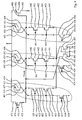
- Figure 3 shows an inventive concept of the present invention.
- Figure 3 shows three circuits 301, 302 and 303, each of which comprises four transistors, a bias transistor 370 and an output transistor 380.
- Circuit 301 comprises four transistors 310, 311, 312 and 313, from which the transistors 310 and 311 forms a structure disclosed with reference to a Figure 2 , and transistors 312 and 313 forms a coefficient coupling disclosed with reference to Figure 1 .
- the transistor 310 functions as the first transistor 201 in Figure 2 , having similar inlets and an outlet, i.e., an inlet 314 for a source voltage, an inlet 315 for a control voltage, and an outlet 316 for providing a current to a following transistor 311.
- the transistor 311 functions as the second transistor 202 in Figure 2 , having similar inlets and an outlet, i.e., an inlet 317 for a source voltage, an inlet 318 for a control voltage, and an outlet 319 for providing an output current.
- Transistors 312 and 313 form a coefficient coupling, which corresponds to the coefficient coupling disclosed with reference to Figure 1 , having similar inlets (320,321, 323 and 324) and outlets (322 and 325).
- the coefficient coupling i.e., transistors 312 and 313 functions the same way as the coefficient coupling in Figure 1 .
- Circuit 302 (circuit 303) comprises the transistors 330-333 (350-353), having inlets and outlets 334-345 (354-365), which correspond to the transistors 310-313 and the inlets and outlets 314-319 of the circuit 301.
- a bias transistor 370 has an inlet 371 for a source voltage, an inlet 372 for a control voltage and an outlet 373 for providing an output current of the bias transistor 370.
- An output transistor 380 in turn, has an inlet 381 for a source voltage, an inlet 382 for a control voltage and an outlet 383 for providing an output current of the system.
- the output current of the output transistor 380 may be conducted e.g., to another processor in a parallel processor network or to a memory unit.
- the apparatus of Figure 3 is capable to evaluate the first, second and third biggest of the output currents of the transistors 310, 330 and 350.
- a skilled person in the art appreciates that even though there is only three circuits presented in this presentation, the number of circuits, and therefore also the number of the output currents of the first transistors, may be different (e.g., four or more), and the same evaluation procedure still applies to the system.
- the added transistor(s) is (are) similar to the first transistor, i.e., in case the first transistor is a PMOS transistor the added transistor(s) is (are) also a PMOS transistor (s) . If the first transistor type is a NMOS transistor, the added transistor(s) is (are) also a NMOS transistor (s) .
- the transistors 380, 311, 331 and 351 are of the same size, and because they have the same control voltage (Vcont) and the same supply voltages, it can be understood that unrestricted output currents of the transistors 380, 311, 331 and 351 are of the same value.
- the output current of the transistor 310 is greater than the output current of the transistor 330, which in turn is greater than the output current of the transistor 350.
- the transistors 311, 331 and 351 which are for example NMOS transistors, provide equal output currents in an unrestricted case.
- the control voltages of the transistors 312, 332 and 352 are of the same value, and the sizes of the transistors 312, 332 and 352 are the same. Even though, the control voltages and the sizes of the transistors 312, 332 and 352 are of the same in this exemplifying presentation, they are of the same size for simplifying the presentation.
- the control voltages and the sizes of the transistors 312, 332 and 352 can differ for example so that the output currents of the transistors 312, 332 and 352 are defined in relation to a weighted coefficient, e.g., the output current of the transistor 332 is three times as big as the values of the output currents of the transistors 312 and 352.
- the unrestricted output current of the transistors 312, 332 and 352 is called a reference current (Iref).
- some of the output currents of transistors 312, 332 and 352 may not be restricted by the accompanying switch transistors 313, 333 and 353, respectively, some of the output currents may be restricted by the switches and some output currents may be 0 corresponding to the three modes of operation described with reference to Figure 1 .
- the equilibrium conditions are controlled by a bias current, the output current of the bias transistor 370, in such a way that the sum of the output currents through switches 313, 333 and 353 equals the output current of the bias transistor 370.
- the output current value of the bias transistor 370 is chosen to be between the reference current value and 0 (with a restriction that the value should not be exactly 0).
- the value of the output current of the bias transistor 370 can be, for example, half of the value of the reference current.
- the equilibrium of the system is as follows.
- the voltage (Vcont) which is also a control voltage of the transistors 311, 331, and 351, will be such a value that the output current value of the transistor 311 will be equal to the output current value of the transistor 310.
- the transistor 313 will conduct part of the output current of the transistor 312, and the value of the output current of the transistor 313 equals to the output current value of the bias transistor 370. Because the value of the output current of the transistor 331 is greater than the value of the output current of the transistor 330, the potential value of the control voltage of the transistor 333 will get so low that the transistor 333 does not conduct the output current of the transistor 332, i.e., the value of the output current of the transistor 333 equals to 0. In this situation, the same may be applied to the circuit 303, i.e., the value of the output current of the transistor 353 will equal to 0.
- the value of the output current of the output transistor 380 will equal to the values of the output currents of the transistors 310 and 311 (which are equal), i.e., the output current of the output transistor 380 equals to the biggest value of the output currents of the transistors.
- the input current value of the bias transistor 370 will be chosen to be between the values of the reference current (Iref) and the reference current multiplied by two (2*Iref), e.g., the value of the input current of the bias transistor 370 is reference current multiplied by 1,5 (1,5*Iref).
- the equilibrium of the system is following.
- the control voltage of the transistors 313, 333, and 353 will be such a value, in which the values of the output currents of the transistors 330 and 331 will be equal.
- the value of the output current of the transistor 310 is bigger than the value of the output current of the transistor 311, and therefore, control voltage of the transistor 313 will grow until the transistor 313 conducts the output current of the transistor 312.
- the output current value of the transistor 333 equals to the value where the output current value of the bias transistor 370 is deducted by the output current value of the transistor 310, which in this case equals to the reference current (Iref). Because the value of the output current of the transistor 351 is greater than the value of the output current of the transistor 350, the potential value of the control voltage of the transistor 353 will get so low that the transistor 353 does not conduct the output current of the transistor 352, i.e., the value of the output current of the transistor 353 equals to 0.
- the output current value of the transistor 331 equals to the output current value of the transistor 330, and because the control voltages of the transistor 331 and the output transistor 380 are equal, also the output current of the system equals the output current of the transistor 330.
- the third biggest value of the output currents of the transistors 310, 330 and 350 will be evaluated, the following process can be applied. It is known that the third biggest output current value is also the smallest output current value, which in this example is the output current value of the transistor 350.
- the bias current between 2*Iref and 3*Iref, for example bias current equals to 2,5*Iref.
- the equilibrium of the system is when the switches 313 and 333 conduct the respective currents and switch 353 conducts a limited amount of the current received from the transistor 352.
- the output current of the output transistor 380 equals to output current of the transistor 351, which also equals to the output current of the transistor 350.
- the present invention enables to find any output current value.
- the bias current value is set between (N-1)*Iref and N*Iref, wherein N equals to the ranked order number that is wanted to be found and Iref is the reference value described in the previous paragraphs.
- the present invention it is possible to use the following formula for a bias current to select the ranked order (e.g., the sixth biggest) input current: N - 1 + N / 2 * Iref
- N 6 and the bias current value therefore equals to 5,5*Iref.
- the analog parallel processor network comprises a plurality of processors.
- the analog parallel processor network further comprises a plurality of memory units.
- the output current of the output transistor 380 is provided to a memory unit in an analog parallel processor network, where from the memory unit can provide a voltage to the inlets 315 (335 and 355 respectively) of the transistors 310 (330 and 350 respectively) of another processor.
- the coefficient coupling shown in Figure 3
- the coupling comprises only one transistor.
- the object of the alternative embodiment of the present invention is to minimize the space required for one processor in the chip. As for achieving this result, the programmable function of the coefficient coupling has to be compromised.
- the transistors 312, 332 and 352 are deleted from the circuits 301, 302 and 303.
- Each one of the transistors 313, 333 and 353 receives a source voltage and provides an output current to further processing according to the switching function of the transistors 313, 333 and 353.
- the source voltage is preferably set low enough in order to keep the unity current (i.e., Iref) practically low.
- Figure 4 shows an alternative embodiment of the inventive concept of the present invention.
- Figure 4 shows three circuits 401, 402 and 403, each of which comprises four transistors, a bias transistor 470 and an output transistor 480.
- Circuit 401 comprises four transistors 410, 411, 412 and 413.
- the transistor 410 has an inlet 414 for a source voltage, an inlet 415 for a control voltage, and an outlet 416 for providing an output current of the transistor 410.
- the transistor 411 has an inlet 417 for a source voltage, an inlet 418 for a control voltage, and an outlet 419 for providing an output current.
- Transistors 412 and 413 form a coefficient coupling having inlets 420, 421, 423 and 424 and outlets 422 and 425.
- the coefficient coupling (i.e., transistors 412 and 413) functions the same way as the coefficient coupling in Figure 3 except the transistors 412 and 413 are of the same type, e.g., PMOS transistors.
- This change of the type of the switching transistor 413 also changes the logic when the switch 413 does or does not conduct to the opposite.
- This change of modes of operation also requires the use of the current mirror 490 to negate the combined current received from the transistors 413, 433 and 453.
- the current mirror 490 has two transistors 491 and 492, which in turn have inlets 493 and 495 and outlets 493 and 496.
- the bias transistor 470 has also been changed to a PMOS transistor.
- the transistor 410 has been changed from a PMOS transistor into a NMOS transistor
- the transistor 411 has been changed from a NMOS transistor into a PMOS transistor.
- Circuit 402 (circuit 403) comprises the transistors 430-433 (450-453), having inlets and outlets 434-445 (454-465), which correspond to transistors 410-413 and the inlets and outlets 414-419 of the circuit 401.
- a bias transistor 470 has an inlet 471 for an input current, an inlet 472 for a control voltage and an outlet 473 for providing an output current of the bias transistor 470.
- An output transistor 480 in turn, has an inlet 481 for an input current, an inlet 482 for a control voltage and an outlet 483 for providing an output current of the system.
- the output current of the output transistor 480 may be conducted e.g., to another processor in a parallel processor network or to a memory unit.
- the alternative embodiment of the present invention is also capable to evaluate the current with a specific ranked order number from the set of the output currents of the transistors 410, 430 and 450.
- the same may be applied to the processors that have e.g., nine circuits, with similar evaluation procedure as applied to the alternative embodiment of the present invention.
- the added transistor(s) is (are) similar to the first transistor, i.e., in case the first transistor is a PMOS transistor the added transistor(s) is (are) also a PMOS transistor(s). If the first transistor type is a NMOS transistor, the added transistor(s) is (are) also a NMOS transistor(s).
- the transistors 480, 411, 431 and 451 are of the same size, and because they have the same control voltage (Vcont) and the same supply voltages, it can be understood that output currents of transistors 480, 411, 431 and 451 are of the same value.
- the output current of the transistor 410 is greater than the output current of the transistor 430, which in turn is greater than the output current of the transistor 450.
- the transistors 411, 431 and 451 provide equal output currents in an unrestricted case.
- the control voltages of the transistors 412, 432 and 452 are assumed here to have the same value, and the sizes of the transistors 412, 432 and 452 are the same.
- the unrestricted output current of transistors 412, 432 and 452 is called a reference current (Iref).
- the output current value of the bias transistor 470 will be set to equal half of the reference current (0,5*Iref).
- the output current of the transistor 492 of the current mirror 490 equals to the output current of the bias transistor 470, i.e., the input current (sum current of the output currents of the transistors 413, 433 and 453) of the current mirror equals to the output current of the bias transistor 470.
- the control voltage (Vcont) has been set to a value, in which the output current of the transistor 411 equals to the output current of the transistor 410, and therefore, the transistor 413 conducts partly the output current of the transistor 412.
- the potential value of the control voltage of the transistor 433 will get so high that the transistor 433 does not conduct the output current of the transistor 432, i.e., the value of the output current of the transistor 433 equals to 0. In this situation, the same may be applied to circuit 403, i.e., the value of the output current of the transistor 453 will equal to 0.
- the value of the output current of the output transistor 480 will equal to the values of the output currents of the transistors 410 and 411 (which are equal), i.e., the output current of the output transistor 480 equals to the biggest value of the output currents of the transistors.
- the other two output currents of the transistors 410, 430 and 450 can be extracted by setting the output current value of the bias transistor 470 to equal 1,5*Iref (when evaluating the second biggest value of the transistors 410, 430 and 450), setting the output current value of the bias transistor 470 to equal 2,5*Iref (when evaluating the third biggest value of the transistors 410, 430 and 450.)
- the formula to find out, which transistor has e.g., the sixth biggest output current value presented with reference to Figure 3 also applies to the alternative embodiment of the present invention described with reference to Figure 4 .
- the coefficient coupling shown in Figure 4
- the coupling comprises only one transistor.
- the transistors 412, 432 and 452 are deleted from the circuits 401, 402 and 403.
- Each one of the transistors 413, 433 and 453 receives a source voltage and provides an output current to further processing according to the switching function of the transistors 413, 433 and 453.
- the source voltage is preferably set low enough in order to keep the unity current (i.e., Iref) practically low.
- the analog parallel processor network comprises a plurality of processors.
- the analog parallel processor network further comprises a plurality of memory units.
- the output current of the output transistor 480 is provided to a memory unit in an analog parallel processor network, where from the memory unit provides a voltage to the inlet 417 (437 and 457 respectively) of the transistors 410 (430 and 450 respectively) of another processor.
- a first transistor receives a source voltage and a control voltage of the system, and forms an output current of the first transistor.
- a second transistor receives a source voltage and a control voltage of the system, and provides an output current of the second transistor (step 502).
- the first transistor tends to feed an output current through the second transistor.
- the result output voltage is in close approximate whether to the source voltage received in the first transistor or to the source voltage received in the second transistor.
- a third transistor receives a source voltage and a coefficient voltage and provides an input current to a fourth transistor (step 503).
- the coefficient voltage received in the third transistor can be programmable.
- the fourth transistor receives an input voltage (which is a control voltage of the fourth transistor) defined by the output currents of the first transistor and the second transistor, and an input current received from the third transistor in the fourth transistor.
- the fourth transistor determines a mode of operation based on the input voltage received from the first transistor and the second transistor, and the input current received from the third transistor. In case the output current value of the first transistor is greater than the output current value of the second transistor, the fourth transistor conducts the whole input current received from the third transistor without restricting the amount of the current provided by the third transistor (step 506). In this case the input current received from the third transistor defines the output current of the fourth transistor. In case the output current of the second transistor is essentially equal to the output current of the first transistor, the fourth transistor conducts a limited amount of the input current received from the third transistor in the fourth transistor (step 507). In this case, the output current of the fourth transistor is between the input current value of the fourth transistor and 0.
- the value of the output current of the fourth transistor equals to an output current value of a bias transistor of the system, if a maximum current is extracted. Otherwise, the value of the output current of the fourth transistor should essentially equal to a value that is the output current of the bias transistor minus (N-1)*Iref, wherein N equals to the ranked order number that is extracted. If the output current value provided by the second transistor is greater than the output current value provided by the first transistor, the potential value of the control voltage of the fourth transistor will get such that the fourth transistor does not conduct the input current received from the third transistor in the fourth transistor (step 508), i.e., the output current of the fourth transistor is essentially equal to 0.
- the output current of the fourth transistor is provided for further processing in the system.
- a control voltage of the second transistor, and other respective transistors in a processor is formed from the output current of the fourth transistor together with other output currents received from respective transistors of the processor.
- the sum current of the output current of the fourth transistor and other output currents received from respective transistors and a bias transistor of the processor forms a control voltage (Vcont), which is conducted to the second transistor and respective transistors in the processor.
- the control voltage (Vcont) is also conducted to a bias transistor.
- the bias transistor output current is set to a value in which a current with a specific ranked order number from the set of the output currents of the first transistors can be determined (step 511).
- the bias current i.e., the output current of the bias transistor
- the bias current controls an equilibrium conditions in such a way that the sum of the output currents of the fourth transistor and its respective transistors in the processor equals to the output current of the bias transistor. This can be implemented because the control voltage of the bias transistor can be programmed to a certain value.
- the step 503 is eliminated, and the 'fourth transistor' (which is a third transistor in the alternative embodiment of the present invention) receives a source voltage directly (in the preferred embodiment of the present invention the third transistor received the source voltage and provided an input current of the fourth transistor to the fourth transistor).
- the alternative embodiment of the present invention corresponds to the preferred embodiment of the invention in other steps than the step 503.
Landscapes
- Physics & Mathematics (AREA)
- General Physics & Mathematics (AREA)
- Engineering & Computer Science (AREA)
- Theoretical Computer Science (AREA)
- Analogue/Digital Conversion (AREA)
- Image Processing (AREA)
- Multi Processors (AREA)
- Processing Or Creating Images (AREA)
- Electronic Switches (AREA)
- Compression Or Coding Systems Of Tv Signals (AREA)
- Communication Control (AREA)
- Power Sources (AREA)
Claims (15)
- Schaltung (301, 302, 303) zur Verarbeitung von Bildern in einem analogen parallelen Prozessornetzwerk, wobei die Schaltung (301, 302, 303) Folgendes aufweist:eine Stromquellenteilschaltung, welche einen ersten MOS-Transistor (310, 330, 350) aufweist, der in Reihe mit einem zweiten MOS-Transistor (311, 331, 351) angeordnet ist, wobei der zweite Transistor (311, 331, 351) in Bezug auf den ersten Transistor (310, 330, 350) ein Komplementärtyp ist, und wobei der erste Transistor (310, 330, 350) zum Empfang jeweiliger Versorgungsspannungen und zur Bereitstellung jeweiliger Ausgangsströme angeordnet ist, wobei eine Ausgangsspannung der Stromquellenteilschaltung durch die Ausgangsströme des ersten und zweiten Transistors festgelegt ist, und wobei der Ausgangsstrom des zweiten Transistors durch eine Summierknotenspannung steuerbar ist; undeine Koeffizientenkopplungsteilschaltung, welche einen dritten Transistor (312, 332, 352) aufweist, der in Reihe mit einem vierten Transistor (313, 333, 353) angeordnet ist, wobei der dritte Transistor (312, 332, 352) zum Empfang einer Versorgungsspannung und zur Bereitstellung eines Ausgangsstroms angeordnet ist, und wobei der vierte Transistor (313, 333, 353) zum Empfang der Ausgangsspannung der Stromquellenteilschaltung als Steuerspannung und des Ausgangsstroms des dritten Transistors (312, 332, 352) als Eingangsstrom und zur Bereitstellung einer Schaltfunktion für einen Ausgangsstrom der Koeffizientenkopplungsteilschaltung, welcher zur Bereitstellung an den Summierknoten vorgesehen ist, angeordnet ist.
- Prozessor in einem analogen parallelen Prozessornetzwerk, zur Bildverarbeitung, wobei der Prozessor Folgendes aufweist:zumindest zwei Schaltungen nach Anspruch 1;einen Vorspannungstransistor (370), welcher funktionell mit dem Summierknoten gekoppelt ist und zur Bereitstellung eines Steuerstroms zur Steuerung der Summe der Ausgangsströme der Koeffizientenkopplungsteilschaltungen vorgesehen ist; undeinen Ausgangstransistor (380), welcher funktionell mit dem Summierknoten gekoppelt ist und zur Bereitstellung eines Ausgangsstroms des Prozessors angeordnet ist, wobei dieser Ausgangsstrom durch die Summierknotenspannung festgelegt ist.
- Prozessor nach Anspruch 2, wobei der Vorspannungstransistor einen Ausgangsstrom bereitstellt, welcher auf einen Wert eingestellt ist, mit welchem ein Strom mit einer spezifischen klassifizierten Ordnungszahl aus dem Satz von Ausgangsströmen des ersten Transistors, oder jeweiligen Transistoren, festlegbar ist.
- Prozessor nach einem der vorhergehenden Ansprüche, wobei jede der Koeffizientenkopplungsteilschaltungen eine von drei Betriebsarten bereitstellt:der vierte Transistor leitet den Ausgangsstrom des begleitenden dritten Transistors;der vierte Transistor leitet einen begrenzten Betrag des Ausgangsstroms des begleitenden dritten Transistors;der vierte Transistor leitet keinen Ausgangsstrom des begleitenden dritten Transistors.
- Prozessor nach einem der vorhergehenden Ansprüche, wobei der dritte Transistor eine Koeffizientenspannung, welche programmierbar ist, empfängt.
- Prozessor nach einem der vorhergehenden Ansprüche, wobei der erste Transistor einen Eingang für die Versorgungsspannung und einen Eingang für eine Steuerspannung aufweist.
- Prozessor nach einem der vorhergehenden Ansprüche, wobei der zweite Transistor einen Eingang für die Versorgungsspannung und einen Eingang für eine Steuerspannung aufweist, wobei die Steuerspannung von einem Ausgangsstrom des vierten Transistors zusammen mit anderen, von jeweiligen Transistoren eines Prozessors und von dem Vorspannungstransistor empfangenen Ausgangsströmen, gebildet ist.
- Prozessor nach einem der vorhergehenden Ansprüche, wobei zumindest einer der Transistoren ein PMOS-Transistor ist.
- Prozessor nach einem der vorhergehenden Ansprüche, wobei zumindest einer der Transistoren ein NMOS-Transistor ist.
- Prozessor nach einem der vorhergehenden Ansprüche, wobei der Prozessor ferner zumindest einen Transistor zur Bereitstellung eines Ausgangsstroms, welcher mit dem Ausgangsstrom des ersten Transistors aufsummierbar ist, aufweist.
- Verfahren zum Verarbeiten von Bildern in einem analogen parallelen Prozessornetzwerk, wobei das Verfahren folgende Verfahrensschritte aufweist:Empfangen einer Sourcespannung und einer Steuerspannung in einem ersten MOS-Transistor (310, 330, 350) und Bilden eines Ausgangsstroms des ersten Transistors;Empfangen einer Sourcespannung und einer Steuerspannung in einem zweiten MOS-Transistor (311, 331, 353), welcher in Reihe mit dem ersten Transistor angeordnet ist, wobei der zweite Transistor in Bezug auf den ersten Transistor ein Komplementärtyp ist, und Bilden eines Ausgangsstroms des zweiten Transistors;Empfangen einer Sourcespannung und einer Koeffizientenspannung in einem dritten MOS-Transistor (312, 332, 352), und Bereitstellen eines Eingangsstroms zu einem vierten Transistor (313, 333, 353);Empfangen einer Eingangsspannung, welche durch die Ausgangsströme des ersten Transistors (310, 330, 350) und des zweiten Transistors (311, 331, 351) festgelegt ist, und eines Eingangsstroms von dem dritten Transistor (312, 332, 352) in den vierten Transistor (313, 333, 353);Aktivieren einer vorher festgelegten Betriebsart in dem vierten Transistor (313, 333, 353) mittels der Eingangsspannung und des Eingangsstroms; undBereitstellen eines Ausgangsstroms des vierten Transistors (313, 333, 353) zur weiteren Verarbeitung.
- Verfahren nach Anspruch 11, wobei die Koeffizientenspannung programmierbar ist.
- Verfahren nach Anspruch 11 oder 12, wobei die vorher festgelegte Betriebsart eine der folgenden ist:der vierte Transistor leitet den Eingangsstrom;der vierte Transistor leitet einen begrenzten Betrag des Eingangsstroms; oderder vierte Transistor leitet keinen Eingangsstrom.
- Verfahren nach einem der Ansprüche 11 bis 13, wobei der Ausgangsstrom des vierten Transistors zum Bilden einer Steuerspannung des zweiten Transistors und weiterer jeweiliger Transistoren in einem Prozessor zusammen mit weiteren, von jeweiligen Transistoren und von einem Vorspannungstransistor des Prozessors in einem analogen parallelen Prozessornetzwerk empfangenen Strömen vorgesehen ist.
- Verfahren nach einem der Ansprüche 11 bis 14, wobei das Verfahren weiterhin einen Vorspannungstransistor aufweist, welcher einen Ausgangsstrom bereitstellt, der auf einen Wert eingestellt wird, mit welchem ein Strom mit einer spezifischen klassifizierten Ordnungszahl aus dem Satz von Ausgangsströmen des ersten Transistors, oder jeweiligen Transistoren, festgelegt wird.
Applications Claiming Priority (3)
| Application Number | Priority Date | Filing Date | Title |
|---|---|---|---|
| FI20002864A FI113714B (fi) | 2000-12-28 | 2000-12-28 | Prosessori, piiri ja menetelmä kuvien käsittelemiseksi rinnakkaisprosessoriverkossa |
| FI20002864 | 2000-12-28 | ||
| PCT/FI2001/001154 WO2002054348A1 (en) | 2000-12-28 | 2001-12-28 | A processor, a circuit and a method for processing images in a parallel processor network |
Publications (2)
| Publication Number | Publication Date |
|---|---|
| EP1346320A1 EP1346320A1 (de) | 2003-09-24 |
| EP1346320B1 true EP1346320B1 (de) | 2008-11-05 |
Family
ID=8559822
Family Applications (1)
| Application Number | Title | Priority Date | Filing Date |
|---|---|---|---|
| EP01994868A Expired - Lifetime EP1346320B1 (de) | 2000-12-28 | 2001-12-28 | Prozessor, Schaltung und Verfahren zur Verarbeitung von Bildern in einem parallelen Prozessornetwerk |
Country Status (8)
| Country | Link |
|---|---|
| US (1) | US7349939B2 (de) |
| EP (1) | EP1346320B1 (de) |
| CN (1) | CN1273905C (de) |
| AT (1) | ATE413667T1 (de) |
| DE (1) | DE60136486D1 (de) |
| ES (1) | ES2315317T3 (de) |
| FI (1) | FI113714B (de) |
| WO (1) | WO2002054348A1 (de) |
Families Citing this family (2)
| Publication number | Priority date | Publication date | Assignee | Title |
|---|---|---|---|---|
| US8150902B2 (en) | 2009-06-19 | 2012-04-03 | Singular Computing Llc | Processing with compact arithmetic processing element |
| US9184744B2 (en) * | 2014-03-14 | 2015-11-10 | Infineon Technologies Ag | Gate signal generation with adaptive signal profiles |
Family Cites Families (11)
| Publication number | Priority date | Publication date | Assignee | Title |
|---|---|---|---|---|
| FR2572822B1 (fr) * | 1984-11-07 | 1986-12-26 | Anizan Paul | Dispositif analogique parallele de traitement local d'un signal bidimensionnel |
| JP3260357B2 (ja) * | 1990-01-24 | 2002-02-25 | 株式会社日立製作所 | 情報処理装置 |
| US5517134A (en) * | 1994-09-16 | 1996-05-14 | Texas Instruments Incorporated | Offset comparator with common mode voltage stability |
| JPH08298663A (ja) * | 1995-04-26 | 1996-11-12 | Canon Inc | 画像処理方法及びその装置 |
| US6011295A (en) * | 1997-07-22 | 2000-01-04 | Foveonics, Inc. | Neural network active pixel cell |
| DE19741209C1 (de) | 1997-09-18 | 1999-01-21 | Siemens Ag | Zellularer Automat als neuronales Netzwerk und dessen Verwendung |
| JP3016381B2 (ja) * | 1997-10-28 | 2000-03-06 | 日本電気株式会社 | バイト入替え演算器 |
| JP3521181B2 (ja) * | 1998-04-23 | 2004-04-19 | 東亜道路工業株式会社 | 表面状態測定装置 |
| US6281730B1 (en) * | 1999-05-13 | 2001-08-28 | National Semiconductor Corporation | Controlled slew rate driver |
| US6448851B1 (en) * | 2001-08-21 | 2002-09-10 | Texas Instruments Incorporated | Amplifier with offset compensation for a high voltage output transistor stage |
| US7034583B1 (en) * | 2004-10-06 | 2006-04-25 | Texas Instruments Incorporated | Versatile system for output energy limiting circuitry |
-
2000
- 2000-12-28 FI FI20002864A patent/FI113714B/fi not_active IP Right Cessation
-
2001
- 2001-12-28 WO PCT/FI2001/001154 patent/WO2002054348A1/en not_active Ceased
- 2001-12-28 CN CNB018228542A patent/CN1273905C/zh not_active Expired - Fee Related
- 2001-12-28 ES ES01994868T patent/ES2315317T3/es not_active Expired - Lifetime
- 2001-12-28 AT AT01994868T patent/ATE413667T1/de not_active IP Right Cessation
- 2001-12-28 EP EP01994868A patent/EP1346320B1/de not_active Expired - Lifetime
- 2001-12-28 DE DE60136486T patent/DE60136486D1/de not_active Expired - Lifetime
- 2001-12-28 US US10/451,152 patent/US7349939B2/en not_active Expired - Fee Related
Also Published As
| Publication number | Publication date |
|---|---|
| EP1346320A1 (de) | 2003-09-24 |
| FI20002864L (fi) | 2002-06-29 |
| ES2315317T3 (es) | 2009-04-01 |
| HK1065621A1 (en) | 2005-02-25 |
| ATE413667T1 (de) | 2008-11-15 |
| CN1273905C (zh) | 2006-09-06 |
| CN1493060A (zh) | 2004-04-28 |
| WO2002054348A1 (en) | 2002-07-11 |
| FI113714B (fi) | 2004-05-31 |
| US20040073594A1 (en) | 2004-04-15 |
| US7349939B2 (en) | 2008-03-25 |
| DE60136486D1 (de) | 2008-12-18 |
| FI20002864A0 (fi) | 2000-12-28 |
Similar Documents
| Publication | Publication Date | Title |
|---|---|---|
| Saari | Mathematical complexity of simple economics | |
| Akritas | Nearest neighbor estimation of a bivariate distribution under random censoring | |
| Moeeni et al. | A robust design methodology for Kanban system design | |
| Munos et al. | Gradient descent approaches to neural-net-based solutions of the Hamilton-Jacobi-Bellman equation | |
| EP1346320B1 (de) | Prozessor, Schaltung und Verfahren zur Verarbeitung von Bildern in einem parallelen Prozessornetwerk | |
| Brouwer | Fuzzy set covering of a set of ordinal attributes without parameter sharing | |
| EP0823684B1 (de) | Halbleiterfunktionsschaltung | |
| Pottosin | Low power assignment of partial states of a parallel automaton | |
| Seibert et al. | Improvements of upstream, semi-Lagrangian numerical advection schemes | |
| Zheng et al. | Non-Asymptotic Analysis of Classical Spectrum Estimators for $ L $-mixing Time-series Data with Unknown Means | |
| Su et al. | A hybrid learning system for image deblurring | |
| Jacobsen | Homgeneous Gaussian Diffusions in Finite Dimensions | |
| Kowalski et al. | Cellular neural network based weighted median filter for real time image processing | |
| Allahverdi et al. | Stochastic proportionate flowshop scheduling with setups | |
| Hikida et al. | Multilevel neural simulation-based inference | |
| Swiatek | Global identification of complex systems with cascade structure | |
| Talaśka et al. | Analog sorting circuit for the application in self-organizing neural networks based on neural gas learning algorithm | |
| Dogaru et al. | Searching for robust chaos in discrete time neural networks using weight space exploration | |
| JPH1063757A (ja) | ベクトル絶対値演算回路 | |
| Szczęsny et al. | FPAA accelerator for machine vision systems | |
| Augusto et al. | Analog fault diagnosis in nonlinear DC circuits with an evolutionary algorithm | |
| Vincent et al. | Evolutionarily stable strategies in multistage biological systems | |
| Güngör | On inclusion probabilities for weighted random sampling without replacement | |
| JP3219915B2 (ja) | 画像圧縮回路 | |
| Almomani | Automatic variance adjusted Bayesian inference with incomplete data under unequal probability sampling |
Legal Events
| Date | Code | Title | Description |
|---|---|---|---|
| PUAI | Public reference made under article 153(3) epc to a published international application that has entered the european phase |
Free format text: ORIGINAL CODE: 0009012 |
|
| 17P | Request for examination filed |
Effective date: 20030619 |
|
| AK | Designated contracting states |
Kind code of ref document: A1 Designated state(s): AT BE CH CY DE DK ES FI FR GB GR IE IT LI LU MC NL PT SE TR |
|
| AX | Request for extension of the european patent |
Extension state: AL LT LV MK RO SI |
|
| 17Q | First examination report despatched |
Effective date: 20061201 |
|
| GRAP | Despatch of communication of intention to grant a patent |
Free format text: ORIGINAL CODE: EPIDOSNIGR1 |
|
| RIC1 | Information provided on ipc code assigned before grant |
Ipc: G06T 1/20 20060101AFI20080602BHEP |
|
| GRAS | Grant fee paid |
Free format text: ORIGINAL CODE: EPIDOSNIGR3 |
|
| GRAA | (expected) grant |
Free format text: ORIGINAL CODE: 0009210 |
|
| AK | Designated contracting states |
Kind code of ref document: B1 Designated state(s): AT BE CH CY DE DK ES FI FR GB GR IE IT LI LU MC NL PT SE TR |
|
| REG | Reference to a national code |
Ref country code: GB Ref legal event code: FG4D |
|
| REG | Reference to a national code |
Ref country code: CH Ref legal event code: EP |
|
| REG | Reference to a national code |
Ref country code: IE Ref legal event code: FG4D |
|
| REF | Corresponds to: |
Ref document number: 60136486 Country of ref document: DE Date of ref document: 20081218 Kind code of ref document: P |
|
| NLV1 | Nl: lapsed or annulled due to failure to fulfill the requirements of art. 29p and 29m of the patents act | ||
| REG | Reference to a national code |
Ref country code: ES Ref legal event code: FG2A Ref document number: 2315317 Country of ref document: ES Kind code of ref document: T3 |
|
| PG25 | Lapsed in a contracting state [announced via postgrant information from national office to epo] |
Ref country code: AT Free format text: LAPSE BECAUSE OF FAILURE TO SUBMIT A TRANSLATION OF THE DESCRIPTION OR TO PAY THE FEE WITHIN THE PRESCRIBED TIME-LIMIT Effective date: 20081105 |
|
| PG25 | Lapsed in a contracting state [announced via postgrant information from national office to epo] |
Ref country code: FI Free format text: LAPSE BECAUSE OF FAILURE TO SUBMIT A TRANSLATION OF THE DESCRIPTION OR TO PAY THE FEE WITHIN THE PRESCRIBED TIME-LIMIT Effective date: 20081105 Ref country code: NL Free format text: LAPSE BECAUSE OF FAILURE TO SUBMIT A TRANSLATION OF THE DESCRIPTION OR TO PAY THE FEE WITHIN THE PRESCRIBED TIME-LIMIT Effective date: 20081105 |
|
| PG25 | Lapsed in a contracting state [announced via postgrant information from national office to epo] |
Ref country code: DK Free format text: LAPSE BECAUSE OF FAILURE TO SUBMIT A TRANSLATION OF THE DESCRIPTION OR TO PAY THE FEE WITHIN THE PRESCRIBED TIME-LIMIT Effective date: 20081105 Ref country code: MC Free format text: LAPSE BECAUSE OF NON-PAYMENT OF DUE FEES Effective date: 20081231 Ref country code: BE Free format text: LAPSE BECAUSE OF FAILURE TO SUBMIT A TRANSLATION OF THE DESCRIPTION OR TO PAY THE FEE WITHIN THE PRESCRIBED TIME-LIMIT Effective date: 20081105 |
|
| REG | Reference to a national code |
Ref country code: CH Ref legal event code: PL |
|
| PG25 | Lapsed in a contracting state [announced via postgrant information from national office to epo] |
Ref country code: PT Free format text: LAPSE BECAUSE OF FAILURE TO SUBMIT A TRANSLATION OF THE DESCRIPTION OR TO PAY THE FEE WITHIN THE PRESCRIBED TIME-LIMIT Effective date: 20090406 Ref country code: SE Free format text: LAPSE BECAUSE OF FAILURE TO SUBMIT A TRANSLATION OF THE DESCRIPTION OR TO PAY THE FEE WITHIN THE PRESCRIBED TIME-LIMIT Effective date: 20090205 |
|
| PLBE | No opposition filed within time limit |
Free format text: ORIGINAL CODE: 0009261 |
|
| STAA | Information on the status of an ep patent application or granted ep patent |
Free format text: STATUS: NO OPPOSITION FILED WITHIN TIME LIMIT |
|
| 26N | No opposition filed |
Effective date: 20090806 |
|
| PG25 | Lapsed in a contracting state [announced via postgrant information from national office to epo] |
Ref country code: CH Free format text: LAPSE BECAUSE OF NON-PAYMENT OF DUE FEES Effective date: 20081231 Ref country code: LI Free format text: LAPSE BECAUSE OF NON-PAYMENT OF DUE FEES Effective date: 20081231 |
|
| PG25 | Lapsed in a contracting state [announced via postgrant information from national office to epo] |
Ref country code: IE Free format text: LAPSE BECAUSE OF NON-PAYMENT OF DUE FEES Effective date: 20081228 |
|
| PG25 | Lapsed in a contracting state [announced via postgrant information from national office to epo] |
Ref country code: LU Free format text: LAPSE BECAUSE OF NON-PAYMENT OF DUE FEES Effective date: 20081228 Ref country code: CY Free format text: LAPSE BECAUSE OF FAILURE TO SUBMIT A TRANSLATION OF THE DESCRIPTION OR TO PAY THE FEE WITHIN THE PRESCRIBED TIME-LIMIT Effective date: 20081105 |
|
| PG25 | Lapsed in a contracting state [announced via postgrant information from national office to epo] |
Ref country code: TR Free format text: LAPSE BECAUSE OF FAILURE TO SUBMIT A TRANSLATION OF THE DESCRIPTION OR TO PAY THE FEE WITHIN THE PRESCRIBED TIME-LIMIT Effective date: 20081105 |
|
| PG25 | Lapsed in a contracting state [announced via postgrant information from national office to epo] |
Ref country code: GR Free format text: LAPSE BECAUSE OF FAILURE TO SUBMIT A TRANSLATION OF THE DESCRIPTION OR TO PAY THE FEE WITHIN THE PRESCRIBED TIME-LIMIT Effective date: 20090206 |
|
| PGFP | Annual fee paid to national office [announced via postgrant information from national office to epo] |
Ref country code: DE Payment date: 20131217 Year of fee payment: 13 Ref country code: GB Payment date: 20131218 Year of fee payment: 13 |
|
| PGFP | Annual fee paid to national office [announced via postgrant information from national office to epo] |
Ref country code: ES Payment date: 20131220 Year of fee payment: 13 Ref country code: IT Payment date: 20131220 Year of fee payment: 13 |
|
| PGFP | Annual fee paid to national office [announced via postgrant information from national office to epo] |
Ref country code: FR Payment date: 20131231 Year of fee payment: 13 |
|
| REG | Reference to a national code |
Ref country code: DE Ref legal event code: R119 Ref document number: 60136486 Country of ref document: DE |
|
| GBPC | Gb: european patent ceased through non-payment of renewal fee |
Effective date: 20141228 |
|
| REG | Reference to a national code |
Ref country code: FR Ref legal event code: ST Effective date: 20150831 |
|
| PG25 | Lapsed in a contracting state [announced via postgrant information from national office to epo] |
Ref country code: DE Free format text: LAPSE BECAUSE OF NON-PAYMENT OF DUE FEES Effective date: 20150701 Ref country code: GB Free format text: LAPSE BECAUSE OF NON-PAYMENT OF DUE FEES Effective date: 20141228 |
|
| PG25 | Lapsed in a contracting state [announced via postgrant information from national office to epo] |
Ref country code: FR Free format text: LAPSE BECAUSE OF NON-PAYMENT OF DUE FEES Effective date: 20141231 |
|
| PG25 | Lapsed in a contracting state [announced via postgrant information from national office to epo] |
Ref country code: IT Free format text: LAPSE BECAUSE OF NON-PAYMENT OF DUE FEES Effective date: 20141228 |
|
| REG | Reference to a national code |
Ref country code: ES Ref legal event code: FD2A Effective date: 20160127 |
|
| PG25 | Lapsed in a contracting state [announced via postgrant information from national office to epo] |
Ref country code: ES Free format text: LAPSE BECAUSE OF NON-PAYMENT OF DUE FEES Effective date: 20141229 |