EP1338084B1 - Power conversion device - Google Patents
Power conversion device Download PDFInfo
- Publication number
- EP1338084B1 EP1338084B1 EP00978043A EP00978043A EP1338084B1 EP 1338084 B1 EP1338084 B1 EP 1338084B1 EP 00978043 A EP00978043 A EP 00978043A EP 00978043 A EP00978043 A EP 00978043A EP 1338084 B1 EP1338084 B1 EP 1338084B1
- Authority
- EP
- European Patent Office
- Prior art keywords
- switching element
- switch
- voltage
- conversion device
- power conversion
- Prior art date
- Legal status (The legal status is an assumption and is not a legal conclusion. Google has not performed a legal analysis and makes no representation as to the accuracy of the status listed.)
- Expired - Lifetime
Links
Images


Classifications
-
- H—ELECTRICITY
- H02—GENERATION; CONVERSION OR DISTRIBUTION OF ELECTRIC POWER
- H02M—APPARATUS FOR CONVERSION BETWEEN AC AND AC, BETWEEN AC AND DC, OR BETWEEN DC AND DC, AND FOR USE WITH MAINS OR SIMILAR POWER SUPPLY SYSTEMS; CONVERSION OF DC OR AC INPUT POWER INTO SURGE OUTPUT POWER; CONTROL OR REGULATION THEREOF
- H02M1/00—Details of apparatus for conversion
- H02M1/36—Means for starting or stopping converters
-
- H—ELECTRICITY
- H02—GENERATION; CONVERSION OR DISTRIBUTION OF ELECTRIC POWER
- H02M—APPARATUS FOR CONVERSION BETWEEN AC AND AC, BETWEEN AC AND DC, OR BETWEEN DC AND DC, AND FOR USE WITH MAINS OR SIMILAR POWER SUPPLY SYSTEMS; CONVERSION OF DC OR AC INPUT POWER INTO SURGE OUTPUT POWER; CONTROL OR REGULATION THEREOF
- H02M7/00—Conversion of AC power input into DC power output; Conversion of DC power input into AC power output
- H02M7/42—Conversion of DC power input into AC power output without possibility of reversal
- H02M7/44—Conversion of DC power input into AC power output without possibility of reversal by static converters
- H02M7/48—Conversion of DC power input into AC power output without possibility of reversal by static converters using discharge tubes with control electrode or semiconductor devices with control electrode
- H02M7/53—Conversion of DC power input into AC power output without possibility of reversal by static converters using discharge tubes with control electrode or semiconductor devices with control electrode using devices of a triode or transistor type requiring continuous application of a control signal
- H02M7/537—Conversion of DC power input into AC power output without possibility of reversal by static converters using discharge tubes with control electrode or semiconductor devices with control electrode using devices of a triode or transistor type requiring continuous application of a control signal using semiconductor devices only, e.g. single switched pulse inverters
- H02M7/5387—Conversion of DC power input into AC power output without possibility of reversal by static converters using discharge tubes with control electrode or semiconductor devices with control electrode using devices of a triode or transistor type requiring continuous application of a control signal using semiconductor devices only, e.g. single switched pulse inverters in a bridge configuration
-
- H—ELECTRICITY
- H02—GENERATION; CONVERSION OR DISTRIBUTION OF ELECTRIC POWER
- H02P—CONTROL OR REGULATION OF ELECTRIC MOTORS, ELECTRIC GENERATORS OR DYNAMO-ELECTRIC CONVERTERS; CONTROLLING TRANSFORMERS, REACTORS OR CHOKE COILS
- H02P1/00—Arrangements for starting electric motors or dynamo-electric converters
- H02P1/16—Arrangements for starting electric motors or dynamo-electric converters for starting dynamo-electric motors or dynamo-electric converters
- H02P1/26—Arrangements for starting electric motors or dynamo-electric converters for starting dynamo-electric motors or dynamo-electric converters for starting an individual polyphase induction motor
-
- H—ELECTRICITY
- H02—GENERATION; CONVERSION OR DISTRIBUTION OF ELECTRIC POWER
- H02P—CONTROL OR REGULATION OF ELECTRIC MOTORS, ELECTRIC GENERATORS OR DYNAMO-ELECTRIC CONVERTERS; CONTROLLING TRANSFORMERS, REACTORS OR CHOKE COILS
- H02P27/00—Arrangements or methods for the control of AC motors characterised by the kind of supply voltage
- H02P27/04—Arrangements or methods for the control of AC motors characterised by the kind of supply voltage using variable-frequency supply voltage, e.g. inverter or converter supply voltage
- H02P27/06—Arrangements or methods for the control of AC motors characterised by the kind of supply voltage using variable-frequency supply voltage, e.g. inverter or converter supply voltage using DC to AC converters or inverters
Definitions
- the present invention relates to a power conversion device; in particular, relates to an improvement thereof to limit an inrush current while reducing overall weight and volume of the device even under a high rated power.
- Fig. 16 is a circuit diagram showing a structure of a conventional power conversion device (which will be hereinafter referred to as "first prior art") having an inrush current limiting circuit.
- This power conversion device 451 comprises an inverter 5, a capacitor 12, a main power source 10, switches 11, 11a, and a resistor 11b.
- the power conversion device 451 is utilized by connecting a three-phase inductive load 50, such as a motor, to output terminals U, V and W of the power conversion device 451.
- the main power source 10 supplies source input terminals P, N of the inverter 5 with a DC (i.e. direct current) main power source voltage V DC1 .
- the capacitor 12 is connected to the source input terminals P, N, and thereby functions to hold a DC voltage supplied to the inverter 5 at a constant level by means of its capacitance C DC .
- the switch 11, structured as a relay, functions as a main switch that turns ON when power supply to the inductive load 5 is started and turns OFF when stopped.
- the switch 11a and the resistor 11b are interposed between the main power source 10 and the capacitor 12 so as to limit an inrush current which flows to charge the capacitor 12 immediately after the switch 11 turns on. After the switch 11 turns ON to start the inverter 5, the switch 11a remains OFF until charging of the capacitor 12 is almost completed. Accordingly, the inrush current is limited by the resistor 11b.
- the switch 11 and the switch 11a have to operate mechanically while a high voltage being applied, the reliability and durability thereof have been problematic. In particular, arcing is influential to the reliability and durability. Moreover, conduction losses of both the switch 11 and the switch 11a during the normal operation of the inverter 5 have also been not negligible concerns.
- Fig. 17 is a circuit diagram showing a structure of another conventional power conversion device (which will be hereinafter referred to as "second prior art") having an inrush current limiting circuit.
- This power conversion device 452 is characteristically different from the power conversion device 451 according to the first prior art in that an NTC (negative coefficient thermistor) 11c is interposed between the main power source 10 and the capacitor 12 in place of the switch 11a and the resistor 11b.
- NTC negative coefficient thermistor
- the NTC 11c is low in temperature, it has high resistance.
- the inrush current flowing after the switch 11 turns ON is, therefore, limited by high resistance of the NTC 11c.
- the temperature of the NTC 11c rapidly rises up due to loss heat generated in the NTC 11c. Accordingly, the resistance of the NTC 11c rapidly decreases, which decreases loss in the NTC 11c.
- the loss generated in the NTC 11c during the operation of the inverter 5 is, however, not negligible, and therefore, the power conversion device 452 has been disadvantageously applicable only to devices having a low rated power (e.g. few kW or less). Further, if the inverter 5 starts operation before the NTC 11c has sufficiently been cooled down, e.g. the inverter 5 restarts immediately after it stopped, the NTC 11c does not sufficiently function as an inrush current limiter, which has also degraded the reliability of the device.
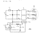
- Fig. 18 is a circuit diagram showing a structure of still another conventional power conversion device (which will be hereinafter referred to as "third prior art") having an inrush current limiting circuit.
- This power conversion device 453 is disclosed in Japanese Patent Application Laid-Open No. 6-115836 (1994), and is characteristically different from any one of the power conversion devices 451 and 452 in that an initial charging circuit for charging the capacitor 12 is connected to the capacitor 12 in parallel.
- the initial charging circuit comprises a reactor 11d, a switching element 11e, a DC power source 11f, a controller unit 11g, a resistor 11h, a base drive circuit 11j and a diode 11k.
- the switch 11 is initially set OFF.
- the switching element 11e repeatedly turns ON and OFF due to the function of the controller unit 11g.
- a current is repeatedly charged into and discharged from the reactor 11d, and the discharged current is repeatedly supplied to the capacitor 12.
- the initial charging circuit functions as such a charge-pumping circuit as to charge up the capacitor 12.
- the initial charging circuit stops its operation and the switch 11 turns on. Thereafter, the inverter 5 starts the normal operation.
- the power conversion device 453 is advantageously applicable to devices having a high rated power, and does advantageously not require any of the switch 11a and the resistor 11b for limiting the inrush current (see Fig. 16).
- the power conversion device 453 needs the reactor 11d and the switching element 11e, which is a power element, and therefore, the power conversion device 453 has been posing a problem in that overall weight and volume are large and a manufacturing cost is high, similarly to the power conversion device 451.
- a first aspect of the present invention is directed to a power conversion device.
- the initial charge controller unit controls the second switching element to turn OFF when a charging current which is a current flowing through the initial charging circuit exceeds a first reference current and turn ON when the charging current drops below a second reference current.
- the initial charge controller unit controls the first switch and the second switch so as to set the first switch OFF and set the second switch ON when a charged voltage which is a voltage across the capacitor is lower than a reference voltage, and set the first switch ON and the second switch OFF when the charged voltage is higher than the reference voltage.
- the initial charging circuit further has a diode connected to the DC power source and the second switch in series.
- the power conversion device further comprises: a rectifier circuit converting an AC voltage input from an exterior into a DC voltage and applying the DC voltage between other source line of the set of the first source line and the second source line and other end of the first switch.
- the DC power source is a converter converting the DC voltage into another DC voltage.
- the power conversion device further comprises: first to fourth drive circuits respectively connected to control electrodes of the first to fourth switching elements, and respectively driving the first to fourth switching elements in response to first to fourth control signals respectively, wherein the initial charge controller unit transmits the second control signal to the second drive circuit to thereby control the second switching element.
- source voltages of the second and fourth drive circuits are supplied by the DC power source.
- the power conversion device further comprises: a charged voltage detection circuit detecting the charged voltage to thereby output a first detection voltage, wherein the initial charge controller unit receives the first detection voltage to thereby control the first switch and the second switch on a basis of the charged voltage.
- the charged voltage detection circuit comprises: a first resistor, one end thereof being connected to the first source line; and a second resistor, one end thereof being connected to other end of the first resistor and other end thereof being connected to the second source line, and outputs a voltage at a connection between the first resistor and the second resistor as the first detection voltage.
- the power conversion device further comprises: a charging current detection circuit detecting the charging current to thereby output a second detection voltage, wherein the initial charge controller unit receives the second detection voltage to thereby control the second switching element on a basis of the charging current.
- the charging current detection circuit comprises a third resistor interposed into a path of the charging current, and outputs a voltage drop across the third resistor as the second detection voltage.
- the power conversion device further comprises: a charged voltage detection circuit detecting the charged voltage to thereby output a first detection voltage; and a charging current detection circuit detecting the charging current to thereby output a second detection voltage
- the initial charge controller unit comprises: an A/D converter converting the first detection voltage and the second detection voltage from analogue form to digital form; a processing unit executing a digital operation processing on a basis of the first and second detection voltages having digital: form to thereby calculate a set of signals which control the first switch, the second switch and the second switching element; and a buffer circuit amplifying the set of signals to thereby transmit the same to the first switch, the second switch and the second switching element.
- the processing unit comprises: a CPU operating on a basis of a program; and a memory storing the program, wherein the CPU operates on a basis of the program so as to calculate the set of signals.
- the power conversion device further comprises: a charged voltage detection circuit detecting the charged voltage to thereby output a first detection voltage; and a charging current detection circuit detecting the charging current to thereby output a second detection voltage
- the initial charge controller unit comprises: a first operational amplifier of two-input type; and a second operational amplifier of two-input type, wherein the first operational amplifier receives, at two inputs thereof, the first detection voltage and a first reference voltage, and transmits an output signal thereof to the first switch and the second switch so as to set only one of the first switch and the second switch ON, and the second operational amplifier has a positive feedback loop, receives the second detection voltage at a reverse input thereof, receives a second reference voltage at a non-reverse input thereof, and transmits an output signal thereof to the second switching element.
- the initial charge controller unit further comprises a logic switch, and the logic switch is interposed into a transmission path transmitting the output signal of the second operational amplifier to second switching element, and transmits the output signal of the second operational amplifier to the second switching element only when an output signal of the first operational amplifier is such a value to set the first switch OFF.
- the initial charge controller unit comprises: a CPU operating on a basis of a program; and a memory storing the program, wherein the CPU operates on a basis of the program so as to control the first switch, the second switch and the second switching element.
- the power conversion device further comprises: a main controller unit controlling the first to fourth switching elements so as to perform a normal operation of the first to fourth switching elements.
- the initial charge controller unit and the main controller unit are integrated into an integrated controller unit which comprises a CPU operating on a basis of a program and a memory storing the program, wherein the CPU operates on a basis of the program so as to perform both a control of the initial charge controller unit and a control of the main controller unit.
- the power conversion device further comprises: a fifth switching element, one main electrode thereof being connected to the first source line; a fifth freewheeling diode connected to the fifth switching element in inverse-parallel; a sixth switching element, one main electrode thereof being connected to other main electrode of the fifth switching element, and other main electrode thereof being connected to the second source line; and a sixth freewheeling diode connected to the sixth switching element in inverse-parallel.
- a main power source is connected between the other source line of the set of the first and second source lines and the other end of the first switch, and an inductive load is connected between two connections.
- One is a connection between the first and second switching elements, and the other is a connection between the third and fourth switching elements.
- the initial charge controller unit, the second switching element and an inductance of the inductive load function as a charge-pumping circuit, so that a charging current is repeatedly charged into and discharged from the inductance of the inductive load and the discharged charging current repeatedly charges the capacitor passing through the first freewheeling diode. If the first switch is turned ON for the normal operation after the capacitor has been sufficiently charged, an inrush current due to turning-ON of the first switch can be suppressed.
- the second switching element repeatedly turns ON and OFF so that the charging current flowing through the initial charging circuit remains within a certain range. Accordingly, the capacitor is charged efficiently in a short time.
- the capacitor is charged with the first switch set OFF and the second switch set ON until the charged voltage across the capacitor reaches the reference voltage.
- the second switch turns OFF so as to isolate the initial charging circuit from the inductive load, and the first switch turns ON so that the first and second source lines are supplied with a DC voltage from the main power source.
- the charging circuit is provided with a diode, the second switch and the DC power source are protected from high voltage being applied.
- the rectifier circuit is provided as a main electrode, the device can be used only by connecting an available. AC power source without preparing an external DC power source.
- the DC power source is a converter which utilizes the DC voltage generated by the rectifier circuit, the DC power source is configured simply.
- the drive circuits for driving the switching elements are provided, small signals are satisfactory as the control signals transmitted to easily drive the switching elements having large rated current. Further, the initial charge controller unit controlling the second switching element can be configured simply.
- the second and fourth drive circuits are supplied with source voltage by the DC power source, an additional power source for supplying the second and fourth drive circuits with the source voltages is not required. Accordingly, the overall weight and volume and the manufacturing cost of the device are further reduced.
- the charged voltage detection circuit is provided, and the detection signal output therefrom is utilized in the initial charge controller unit.
- the initial charge controller unit can, therefore, process a voltage signal having a value suited for processing, so that the initial charge controller unit can be configured simply.
- the charged voltage detection circuit is formed simply of a serial circuit of the first and second resistors, and divided voltage of the charged voltage is output as the first detection voltage.
- the first detection voltage proportional to the charged voltage is obtained by a simple configuration. Further, the first detection voltage can easily be adjusted to a value suited for the processing of the initial charge controller unit by adjusting the resistance ratio of the first and second resistors.
- the charging current detection circuit is provided, and the detection signal output therefrom is utilized in the initial charge controller unit.
- the initial charge controller unit can, therefore, process a voltage signal having a value suited for processing, so that the initial charge controller unit can be configured simply.
- the charging current detection circuit comprises the third resistor interposed into the path of the charging current, and the voltage drop across the third resistor is output as the second detection voltage.
- the charging current detection circuit is configured simply.
- the initial charge controller unit converts the first and second detection voltages into digital signals, and executes the digital operation processing on the basis of the digital signals to thereby peform the control operation. Accordingly, highly precise control operation with little secular change is implemented.
- the CPU operates on the basis of the program stored in the memory so as to perform the control operation of the initial charge controller unit.
- the reference voltage, reference current, processing speed and other conditions can, therefore, be adjusted with high accuracy, and it is easy to adjust or modify these conditions.
- further precise control operation is implemented, and flexible design change suitable for so called multi-item small-quantity production is facilitated.
- the first and second operational amplifiers process the first and second detection voltages so as to perform the control operation of the initial charge controller unit.
- the initial charge controller unit is, therefore, configured simply and lightly, and the manufacturing cost of the device is reduced.
- the initial charge controller unit comprises the logic switch
- the output signal of the second operational amplifier stops being stransmitted to the second switching element when the charged voltage has exceeded the reference voltage and the normal operation has been started.
- the initial charge controller unit therefore, is prevented from intervening the normal operation of the first to fourth switching elements.
- the CPU operates on the basis of the program stored in the memory so as to perform the control operation of the initial charge controller unit.
- the reference voltage, reference current, processing speed and other conditions can, therefore, be adjusted with high accuracy, and it is easy to adjust or modify these conditions.
- further precise control operation is implemented, and flexible design change suitable for so-called multi-item small-quantity production is facilitated.
- the main controller unit controlling the normal operation of the first to fourth switching elements since the main controller unit controlling the normal operation of the first to fourth switching elements is provided, it is not required to input signals driving the first to fourth switching elements from the exterior to perform the normal operation.
- the CPU since the CPU operates on the basis of the program stored in the memory so as to perform the control operation of both the initial charge controller unit and the main controller unit.
- the main controller unit and the initial charge controller unit are configured simply and lightly as a whole, and the manufacturing cost of the device is reduced.
- a three-phase inductive load can be connected as the inductive load.
- Fig. 1 is a circuit diagram showing a structure of a power conversion device according to the first preferred embodiment of the present invention.
- the same reference characters are allotted to the same parts or the corresponding parts (i.e. parts having the same functions) as those in the conventional devices shown in Figs. 16 to 18 so as to make clear the relationship therebetween.
- the power conversion device 401 shown in Fig. 1 comprises an inverter 5, a capacitor 12, a main power source 10, a switch 11, an initial charging circuit 6, resistors 13, 14, an initial charge controller unit 70, and a main controller unit 200.
- the power conversion device 401 is utilized by connecting a three-phase inductive load 50, such as a motor, to output terminals U, V and W of the power conversion device 401.
- the three phase inductive load 50 comprises windings 51, 52 and 53 which have inductances L u , L v and L w , respectively.
- Collectors of the switching elements 21, 31 and 41 are connected to a higher potential source line PP.
- Collectors of the switching elements 24, 34 and 44 are connected to emitters of the switching elements 21, 31 and 41, respectively, and emitters are connected to a lower potential source line NN.
- An output terminal U is connected to a connection between the switching elements 21 and 24.
- An output terminal V is connected to a connection between the switching elements 31 and 34.
- An output terminals W is connected to a connection between the switching elements 41 and 44.
- Freewheeling diodes 22, 25, 32, 35, 42 and 45 are respectively connected in parallel to the switching elements 21, 24, 31, 34, 41 and 44, in such a direction that a forward current flows through corresponding switching element and diode in circular. In the present specification, it is referred to as "connected in inverse-parallel" that a freewheeling diode is connected to a switching element in such a direction that the forward current flows in circular.
- the freewheeling diodes 22, 25, 32, 35, 42 and 45 are provided in order to protect the switching elements 21, 24, 31, 34, 41 and 44 from reverse currents, respectively.
- Switch 18 is structured as a relay.
- the charged voltage detection circuit comprises the resistors 13 and 14.
- One end of the resistor 13 is connected to the higher potential source line PP.
- One end of the resistor 14 is connected to the other end of the resistor 13, and the other end thereof is connected to the lower potential source line NN.
- the voltage at a connection between the resistors 13 and 14 is output as a detection voltage V DC4 .
- the detection voltage V DC4 is obtained by dividing the main power source voltage V DC4 by resistances R1 and R2 of the resistors 13 and 14.
- the DC voltage V DC3 is set sufficiently lower than the main power source voltage V DC1 , and the output impedance of the DC power source 16 is set sufficiently higher than that of the main power source 10.
- the internal impedance thereof can easily set high.
- the charging current I CHG is limited to such a small value as not to burden the DC power source 16 with a heavy load.
- the contact resistance of the switch 18, the on-resistance of the diode 19, and the on-resistance of the freewheeling diode 32 also contribute to limitation of the charging current I CHG .
- the initial charge controller unit 70 transmits the control signal U N to turn OFF the switching element 24 (see (B) and (C) of Fig. 2).
- the reference current I Max is set not larger than a maximum allowed current charging the capacitor 12.
- the energy stored within the capacitor 12 will not discharge through the switching element 24 even when the switching element 24 is set ON, because the freewheeling diodes 22, 32 and 42 are reversely biased.
- the discharge of energy from the capacitor 12 during the initial charging period results only from a current I 3 flowing through the resistors 13 and 14 which is usually negligible because of such high resistances of these resistors as hundreds of kilo-Ohm.
- the switching element 24 repeatedly turns ON and OFF (see (B) of Fig. 2). As a result, the charged voltage across the capacitor 12 is gradually stepped up (see (A) of Fig. 2).
- the initial controller unit 70 transmits the control signals Rel 1 , Rel 2 and U N so as to turn OFF the switch 18 and the switching element 24 and turn ON the switch 11 (see (A) to (E) of Fig. 2).
- the initial charging operation is completed, and the normal operation is started.
- the reference voltage is set at a value closely representing the main power source voltage V DC1 .
- the time required to finish the initial charging operation depends on various parameters including: the capacitance C DC of the capacitor 12, the inductances L u and L v of the inductive load 50, the main power source voltage V DC1 of the main power source 10, the DC voltage V DC3 of the DC power source 16, the reference currents I Max and I Min , and the total resistances R T ⁇ 1 and R T ⁇ 2 within the path of the charging current I CHG .
- the output voltage of the operational amplifier 80 is adjusted by a resistor 73 having a resistance Ro1 and a Zener diode 78 having a Zener voltage V z1 .
- the relation between an adjusted output voltage Vo1 and the detection voltage V DC4 is shown in a graph of Fig. 6.
- the reference voltage V Ref1 is set at such a level that the detection voltage V DC4 reaches the reference voltage V Ref1 as the charged voltage V DC reaches a reference voltage which allows the initial charging operation to be finished.
- the output voltage of the operational amplifier 81 is adjusted by a resistor 77 having a resistance Ro2 and a Zener diode 79 having a Zener voltage V z2 .
- the relation between an adjusted output voltage Vo2 and the detection voltage V CHG is shown in a graph of Fig. 7.
- the reference voltage V Ref2 is set at such a level that the detection voltage V CHG reaches the Max.
- a processing unit 93 executes a digital operation processing on the basis of the detection voltages V DC4 and V CHG having digital form to thereby calculate control signals Rel1, Rel2 and U N which control the switch 11, the switch 18 and the switching element 24.
- a buffer circuit 94 provided at an output stage amplifies the control signals Rel1, Rel2 and U N through buffers 95, 96 and 97 to thereby transmit the same to the switch 11, the switch 18 and the drive circuit 23, respectively.
- the initial charge controller unit 70 is configured as Fig. 8 shows.
- the circuit parameters used in the simulation are as follows:
- Figs. 10 and 11 are graphs showing the result of the simulation.
- Fig. 11 shows final stage of Fig. 10 in detail by enlarging the time scale.
- the result of the simulation has proven the successful operation of the power conversion device 401.
- Fig. 14 is a circuit diagram showing a structure of a power conversion device according to the fourth preferred embodiment of the present invention.
- This power conversion device 404 is characteristically different from the power conversion device 401 according to the first preferred embodiment in that source voltages of the drive circuits 23, 33 and 43 are supplied by the DC power source 16.
- an additional power source for supplying the drive circuits 23, 33 and 43 with the source voltages is advantageously not needed.
- the current capability of the DC power source 16 must satisfy the requirements for both the initial charging operation and the operation of the drive circuits 23, 33 and 43, the overall weight and volume and the manufacturing cost of the device are further reduced.
- the power conversion device 405 is used by connecting a single-phase inductive load 55.
- an inductance Luv of the winding 56 provided in the inductive load 55 functions in equivalent way to the inductances L u and L v in the power conversion device 401 according to the first preferred embodiment. Accordingly, the power conversion device 405 implements the initial charging operation equivalent to that of the power conversion device 401.
Landscapes
- Engineering & Computer Science (AREA)
- Power Engineering (AREA)
- Inverter Devices (AREA)
Applications Claiming Priority (1)
| Application Number | Priority Date | Filing Date | Title |
|---|---|---|---|
| PCT/JP2000/008491 WO2002045250A1 (en) | 2000-11-30 | 2000-11-30 | Power conversion device |
Publications (2)
| Publication Number | Publication Date |
|---|---|
| EP1338084A1 EP1338084A1 (en) | 2003-08-27 |
| EP1338084B1 true EP1338084B1 (en) | 2006-04-12 |
Family
ID=11736746
Family Applications (1)
| Application Number | Title | Priority Date | Filing Date |
|---|---|---|---|
| EP00978043A Expired - Lifetime EP1338084B1 (en) | 2000-11-30 | 2000-11-30 | Power conversion device |
Country Status (4)
| Country | Link |
|---|---|
| EP (1) | EP1338084B1 (enExample) |
| JP (1) | JP4272426B2 (enExample) |
| DE (1) | DE60027333T2 (enExample) |
| WO (1) | WO2002045250A1 (enExample) |
Families Citing this family (4)
| Publication number | Priority date | Publication date | Assignee | Title |
|---|---|---|---|---|
| CN101243590B (zh) | 2005-08-18 | 2010-12-29 | 西门子工业公司 | 用于限制交流涌流的系统和方法 |
| JP5991279B2 (ja) * | 2013-07-18 | 2016-09-14 | トヨタ車体株式会社 | モータ駆動装置 |
| RU2699012C1 (ru) * | 2018-11-26 | 2019-09-03 | Илья Николаевич Джус | Трехфазный частотный преобразователь высокого напряжения |
| CN116667345B (zh) * | 2023-07-31 | 2024-03-19 | 广东电网有限责任公司佛山供电局 | 一种串并联型多端口柔性互联设备的充电控制方法及装置 |
Family Cites Families (6)
| Publication number | Priority date | Publication date | Assignee | Title |
|---|---|---|---|---|
| JPH04355673A (ja) * | 1991-05-31 | 1992-12-09 | Toshiba Corp | 冷凍機のインバータの制御装置 |
| JPH05176554A (ja) * | 1991-12-24 | 1993-07-13 | Shinko Electric Co Ltd | バッテリ内蔵エンジン式発電装置 |
| JPH05344605A (ja) * | 1992-06-05 | 1993-12-24 | Fuji Electric Co Ltd | 電気自動車の電気システム |
| JP3493672B2 (ja) * | 1992-10-06 | 2004-02-03 | 三菱電機株式会社 | エレベータのインバータ装置 |
| JP3334329B2 (ja) * | 1994-05-16 | 2002-10-15 | 三菱電機株式会社 | インバ−タ装置及びエレベ−タの制御装置 |
| JP4284478B2 (ja) * | 1998-12-28 | 2009-06-24 | 株式会社安川電機 | インバータ装置 |
-
2000
- 2000-11-30 JP JP2002546277A patent/JP4272426B2/ja not_active Expired - Lifetime
- 2000-11-30 DE DE60027333T patent/DE60027333T2/de not_active Expired - Lifetime
- 2000-11-30 WO PCT/JP2000/008491 patent/WO2002045250A1/en not_active Ceased
- 2000-11-30 EP EP00978043A patent/EP1338084B1/en not_active Expired - Lifetime
Also Published As
| Publication number | Publication date |
|---|---|
| DE60027333T2 (de) | 2007-01-18 |
| JP2004515199A (ja) | 2004-05-20 |
| WO2002045250A1 (en) | 2002-06-06 |
| JP4272426B2 (ja) | 2009-06-03 |
| EP1338084A1 (en) | 2003-08-27 |
| DE60027333D1 (de) | 2006-05-24 |
Similar Documents
| Publication | Publication Date | Title |
|---|---|---|
| US6654262B2 (en) | Inverter with pre-charging capacitor to reduce inrush current | |
| US9166499B2 (en) | Electronic circuit operating based on isolated switching power source | |
| US8618753B2 (en) | Inverter device | |
| US5889392A (en) | Switch-mode regulators and methods providing transient response speed-up | |
| US8374005B2 (en) | Direct AC power converting apparatus | |
| US6735098B2 (en) | Inrush current limiting circuit, power source device and power conversion device | |
| US20100246217A1 (en) | Direct ac power converting apparatus | |
| US20110007531A1 (en) | Direct ac power converting apparatus | |
| TWI882488B (zh) | 適應性預充控制電路 | |
| US6856525B2 (en) | Apparatus and method for controlling voltage regulator and power supply apparatus | |
| EP1146620A2 (en) | Driving method of semiconductor switching device and power supply apparatus operated according to said method | |
| JP7436142B2 (ja) | 駆動ユニット、電気パワーコンバータ、車両、および電気パワーコンバータの駆動方法 | |
| US10050578B2 (en) | Motor control system, initial charger, and method for detecting failure | |
| JP3416219B2 (ja) | 電源装置 | |
| US12206401B2 (en) | Drive device to drive semiconductor element, semiconductor device, and power conversion device | |
| EP1338084B1 (en) | Power conversion device | |
| CN113949031B (zh) | 电机保护器的电源装置及其供电方法 | |
| JP2778485B2 (ja) | 無停電電源装置 | |
| US11831259B2 (en) | Motor control apparatus | |
| JP2001078447A (ja) | スイッチング電源回路 | |
| EP4372940A1 (en) | Power controller with current limiting function for pre-charging | |
| JPH04275002A (ja) | 電気自動車用充電装置 | |
| JP3608868B2 (ja) | 磁気共鳴イメージング装置用電源装置 | |
| JP3396994B2 (ja) | 多出力dc−dcコンバータ | |
| US11949341B2 (en) | Power converter and electric motor braking method |
Legal Events
| Date | Code | Title | Description |
|---|---|---|---|
| PUAI | Public reference made under article 153(3) epc to a published international application that has entered the european phase |
Free format text: ORIGINAL CODE: 0009012 |
|
| 17P | Request for examination filed |
Effective date: 20020723 |
|
| AK | Designated contracting states |
Designated state(s): AT BE CH CY DE DK ES FI FR GB GR IE IT LI LU MC NL PT SE TR |
|
| AX | Request for extension of the european patent |
Extension state: AL LT LV MK RO SI |
|
| RBV | Designated contracting states (corrected) |
Designated state(s): DE FR IT |
|
| GRAP | Despatch of communication of intention to grant a patent |
Free format text: ORIGINAL CODE: EPIDOSNIGR1 |
|
| RIN1 | Information on inventor provided before grant (corrected) |
Inventor name: HIYAMA, KAZUAKI Inventor name: HUSSEIN, KHALID HASSAN |
|
| GRAS | Grant fee paid |
Free format text: ORIGINAL CODE: EPIDOSNIGR3 |
|
| GRAA | (expected) grant |
Free format text: ORIGINAL CODE: 0009210 |
|
| AK | Designated contracting states |
Kind code of ref document: B1 Designated state(s): DE FR IT |
|
| PG25 | Lapsed in a contracting state [announced via postgrant information from national office to epo] |
Ref country code: IT Free format text: LAPSE BECAUSE OF FAILURE TO SUBMIT A TRANSLATION OF THE DESCRIPTION OR TO PAY THE FEE WITHIN THE PRESCRIBED TIME-LIMIT;WARNING: LAPSES OF ITALIAN PATENTS WITH EFFECTIVE DATE BEFORE 2007 MAY HAVE OCCURRED AT ANY TIME BEFORE 2007. THE CORRECT EFFECTIVE DATE MAY BE DIFFERENT FROM THE ONE RECORDED. Effective date: 20060412 |
|
| RIC1 | Information provided on ipc code assigned before grant |
Ipc: H02M 7/5387 20060101AFI20060220BHEP Ipc: H02P 27/08 20060101ALI20060220BHEP |
|
| RAP2 | Party data changed (patent owner data changed or rights of a patent transferred) |
Owner name: MITSUBISHI DENKI KABUSHIKI KAISHA |
|
| REF | Corresponds to: |
Ref document number: 60027333 Country of ref document: DE Date of ref document: 20060524 Kind code of ref document: P |
|
| ET | Fr: translation filed | ||
| PLBE | No opposition filed within time limit |
Free format text: ORIGINAL CODE: 0009261 |
|
| STAA | Information on the status of an ep patent application or granted ep patent |
Free format text: STATUS: NO OPPOSITION FILED WITHIN TIME LIMIT |
|
| 26N | No opposition filed |
Effective date: 20070115 |
|
| PGFP | Annual fee paid to national office [announced via postgrant information from national office to epo] |
Ref country code: FR Payment date: 20111118 Year of fee payment: 12 |
|
| PGFP | Annual fee paid to national office [announced via postgrant information from national office to epo] |
Ref country code: IT Payment date: 20111111 Year of fee payment: 12 |
|
| REG | Reference to a national code |
Ref country code: FR Ref legal event code: ST Effective date: 20130731 |
|
| PG25 | Lapsed in a contracting state [announced via postgrant information from national office to epo] |
Ref country code: IT Free format text: LAPSE BECAUSE OF NON-PAYMENT OF DUE FEES Effective date: 20121130 |
|
| PG25 | Lapsed in a contracting state [announced via postgrant information from national office to epo] |
Ref country code: FR Free format text: LAPSE BECAUSE OF NON-PAYMENT OF DUE FEES Effective date: 20121130 |
|
| PGFP | Annual fee paid to national office [announced via postgrant information from national office to epo] |
Ref country code: DE Payment date: 20191119 Year of fee payment: 20 |
|
| REG | Reference to a national code |
Ref country code: DE Ref legal event code: R071 Ref document number: 60027333 Country of ref document: DE |