EP1333482A2 - Method for manufacturing a semiconductor silicon carbide on insulator substrate (SOI) and apparatus therefore - Google Patents
Method for manufacturing a semiconductor silicon carbide on insulator substrate (SOI) and apparatus therefore Download PDFInfo
- Publication number
- EP1333482A2 EP1333482A2 EP03250583A EP03250583A EP1333482A2 EP 1333482 A2 EP1333482 A2 EP 1333482A2 EP 03250583 A EP03250583 A EP 03250583A EP 03250583 A EP03250583 A EP 03250583A EP 1333482 A2 EP1333482 A2 EP 1333482A2
- Authority
- EP
- European Patent Office
- Prior art keywords
- gas
- thin film
- silicon carbide
- heating furnace
- soi substrate
- Prior art date
- Legal status (The legal status is an assumption and is not a legal conclusion. Google has not performed a legal analysis and makes no representation as to the accuracy of the status listed.)
- Granted
Links
Images


Classifications
-
- H—ELECTRICITY
- H10—SEMICONDUCTOR DEVICES; ELECTRIC SOLID-STATE DEVICES NOT OTHERWISE PROVIDED FOR
- H10P—GENERIC PROCESSES OR APPARATUS FOR THE MANUFACTURE OR TREATMENT OF DEVICES COVERED BY CLASS H10
- H10P90/00—Preparation of wafers not covered by a single main group of this subclass, e.g. wafer reinforcement
- H10P90/19—Preparing inhomogeneous wafers
- H10P90/1904—Preparing vertically inhomogeneous wafers
- H10P90/1906—Preparing SOI wafers
-
- G—PHYSICS
- G06—COMPUTING OR CALCULATING; COUNTING
- G06Q—INFORMATION AND COMMUNICATION TECHNOLOGY [ICT] SPECIALLY ADAPTED FOR ADMINISTRATIVE, COMMERCIAL, FINANCIAL, MANAGERIAL OR SUPERVISORY PURPOSES; SYSTEMS OR METHODS SPECIALLY ADAPTED FOR ADMINISTRATIVE, COMMERCIAL, FINANCIAL, MANAGERIAL OR SUPERVISORY PURPOSES, NOT OTHERWISE PROVIDED FOR
- G06Q50/00—Information and communication technology [ICT] specially adapted for implementation of business processes of specific business sectors, e.g. utilities or tourism
- G06Q50/10—Services
-
- G—PHYSICS
- G06—COMPUTING OR CALCULATING; COUNTING
- G06Q—INFORMATION AND COMMUNICATION TECHNOLOGY [ICT] SPECIALLY ADAPTED FOR ADMINISTRATIVE, COMMERCIAL, FINANCIAL, MANAGERIAL OR SUPERVISORY PURPOSES; SYSTEMS OR METHODS SPECIALLY ADAPTED FOR ADMINISTRATIVE, COMMERCIAL, FINANCIAL, MANAGERIAL OR SUPERVISORY PURPOSES, NOT OTHERWISE PROVIDED FOR
- G06Q30/00—Commerce
- G06Q30/06—Buying, selling or leasing transactions
- G06Q30/0601—Electronic shopping [e-shopping]
- G06Q30/0613—Electronic shopping [e-shopping] using intermediate agents
- G06Q30/0619—Neutral agent
-
- G—PHYSICS
- G16—INFORMATION AND COMMUNICATION TECHNOLOGY [ICT] SPECIALLY ADAPTED FOR SPECIFIC APPLICATION FIELDS
- G16H—HEALTHCARE INFORMATICS, i.e. INFORMATION AND COMMUNICATION TECHNOLOGY [ICT] SPECIALLY ADAPTED FOR THE HANDLING OR PROCESSING OF MEDICAL OR HEALTHCARE DATA
- G16H20/00—ICT specially adapted for therapies or health-improving plans, e.g. for handling prescriptions, for steering therapy or for monitoring patient compliance
- G16H20/30—ICT specially adapted for therapies or health-improving plans, e.g. for handling prescriptions, for steering therapy or for monitoring patient compliance relating to physical therapies or activities, e.g. physiotherapy, acupressure or exercising
-
- H—ELECTRICITY
- H10—SEMICONDUCTOR DEVICES; ELECTRIC SOLID-STATE DEVICES NOT OTHERWISE PROVIDED FOR
- H10D—INORGANIC ELECTRIC SEMICONDUCTOR DEVICES
- H10D62/00—Semiconductor bodies, or regions thereof, of devices having potential barriers
- H10D62/80—Semiconductor bodies, or regions thereof, of devices having potential barriers characterised by the materials
- H10D62/83—Semiconductor bodies, or regions thereof, of devices having potential barriers characterised by the materials being Group IV materials, e.g. B-doped Si or undoped Ge
- H10D62/832—Semiconductor bodies, or regions thereof, of devices having potential barriers characterised by the materials being Group IV materials, e.g. B-doped Si or undoped Ge being Group IV materials comprising two or more elements, e.g. SiGe
- H10D62/8325—Silicon carbide
-
- H—ELECTRICITY
- H10—SEMICONDUCTOR DEVICES; ELECTRIC SOLID-STATE DEVICES NOT OTHERWISE PROVIDED FOR
- H10P—GENERIC PROCESSES OR APPARATUS FOR THE MANUFACTURE OR TREATMENT OF DEVICES COVERED BY CLASS H10
- H10P14/00—Formation of materials, e.g. in the shape of layers or pillars
- H10P14/20—Formation of materials, e.g. in the shape of layers or pillars of semiconductor materials
-
- H—ELECTRICITY
- H10—SEMICONDUCTOR DEVICES; ELECTRIC SOLID-STATE DEVICES NOT OTHERWISE PROVIDED FOR
- H10P—GENERIC PROCESSES OR APPARATUS FOR THE MANUFACTURE OR TREATMENT OF DEVICES COVERED BY CLASS H10
- H10P14/00—Formation of materials, e.g. in the shape of layers or pillars
- H10P14/20—Formation of materials, e.g. in the shape of layers or pillars of semiconductor materials
- H10P14/27—Formation of materials, e.g. in the shape of layers or pillars of semiconductor materials using selective deposition, e.g. simultaneous growth of monocrystalline and non-monocrystalline semiconductor materials
- H10P14/271—Formation of materials, e.g. in the shape of layers or pillars of semiconductor materials using selective deposition, e.g. simultaneous growth of monocrystalline and non-monocrystalline semiconductor materials characterised by the preparation of substrate for selective deposition
-
- H—ELECTRICITY
- H10—SEMICONDUCTOR DEVICES; ELECTRIC SOLID-STATE DEVICES NOT OTHERWISE PROVIDED FOR
- H10P—GENERIC PROCESSES OR APPARATUS FOR THE MANUFACTURE OR TREATMENT OF DEVICES COVERED BY CLASS H10
- H10P14/00—Formation of materials, e.g. in the shape of layers or pillars
- H10P14/20—Formation of materials, e.g. in the shape of layers or pillars of semiconductor materials
- H10P14/29—Formation of materials, e.g. in the shape of layers or pillars of semiconductor materials characterised by the substrates
- H10P14/2901—Materials
- H10P14/2902—Materials being Group IVA materials
- H10P14/2904—Silicon carbide
-
- H—ELECTRICITY
- H10—SEMICONDUCTOR DEVICES; ELECTRIC SOLID-STATE DEVICES NOT OTHERWISE PROVIDED FOR
- H10P—GENERIC PROCESSES OR APPARATUS FOR THE MANUFACTURE OR TREATMENT OF DEVICES COVERED BY CLASS H10
- H10P14/00—Formation of materials, e.g. in the shape of layers or pillars
- H10P14/20—Formation of materials, e.g. in the shape of layers or pillars of semiconductor materials
- H10P14/29—Formation of materials, e.g. in the shape of layers or pillars of semiconductor materials characterised by the substrates
- H10P14/2901—Materials
- H10P14/2902—Materials being Group IVA materials
- H10P14/2905—Silicon, silicon germanium or germanium
-
- H—ELECTRICITY
- H10—SEMICONDUCTOR DEVICES; ELECTRIC SOLID-STATE DEVICES NOT OTHERWISE PROVIDED FOR
- H10P—GENERIC PROCESSES OR APPARATUS FOR THE MANUFACTURE OR TREATMENT OF DEVICES COVERED BY CLASS H10
- H10P14/00—Formation of materials, e.g. in the shape of layers or pillars
- H10P14/20—Formation of materials, e.g. in the shape of layers or pillars of semiconductor materials
- H10P14/32—Formation of materials, e.g. in the shape of layers or pillars of semiconductor materials characterised by intermediate layers between substrates and deposited layers
- H10P14/3202—Materials thereof
- H10P14/3238—Materials thereof being insulating materials
-
- H—ELECTRICITY
- H10—SEMICONDUCTOR DEVICES; ELECTRIC SOLID-STATE DEVICES NOT OTHERWISE PROVIDED FOR
- H10P—GENERIC PROCESSES OR APPARATUS FOR THE MANUFACTURE OR TREATMENT OF DEVICES COVERED BY CLASS H10
- H10P14/00—Formation of materials, e.g. in the shape of layers or pillars
- H10P14/20—Formation of materials, e.g. in the shape of layers or pillars of semiconductor materials
- H10P14/34—Deposited materials, e.g. layers
- H10P14/3402—Deposited materials, e.g. layers characterised by the chemical composition
- H10P14/3404—Deposited materials, e.g. layers characterised by the chemical composition being Group IVA materials
- H10P14/3408—Silicon carbide
-
- H—ELECTRICITY
- H10—SEMICONDUCTOR DEVICES; ELECTRIC SOLID-STATE DEVICES NOT OTHERWISE PROVIDED FOR
- H10P—GENERIC PROCESSES OR APPARATUS FOR THE MANUFACTURE OR TREATMENT OF DEVICES COVERED BY CLASS H10
- H10P14/00—Formation of materials, e.g. in the shape of layers or pillars
- H10P14/20—Formation of materials, e.g. in the shape of layers or pillars of semiconductor materials
- H10P14/34—Deposited materials, e.g. layers
- H10P14/3402—Deposited materials, e.g. layers characterised by the chemical composition
- H10P14/3404—Deposited materials, e.g. layers characterised by the chemical composition being Group IVA materials
- H10P14/3411—Silicon, silicon germanium or germanium
-
- H—ELECTRICITY
- H10—SEMICONDUCTOR DEVICES; ELECTRIC SOLID-STATE DEVICES NOT OTHERWISE PROVIDED FOR
- H10P—GENERIC PROCESSES OR APPARATUS FOR THE MANUFACTURE OR TREATMENT OF DEVICES COVERED BY CLASS H10
- H10P90/00—Preparation of wafers not covered by a single main group of this subclass, e.g. wafer reinforcement
- H10P90/19—Preparing inhomogeneous wafers
- H10P90/1904—Preparing vertically inhomogeneous wafers
- H10P90/1906—Preparing SOI wafers
- H10P90/1914—Preparing SOI wafers using bonding
-
- H—ELECTRICITY
- H10—SEMICONDUCTOR DEVICES; ELECTRIC SOLID-STATE DEVICES NOT OTHERWISE PROVIDED FOR
- H10W—GENERIC PACKAGES, INTERCONNECTIONS, CONNECTORS OR OTHER CONSTRUCTIONAL DETAILS OF DEVICES COVERED BY CLASS H10
- H10W10/00—Isolation regions in semiconductor bodies between components of integrated devices
-
- H—ELECTRICITY
- H10—SEMICONDUCTOR DEVICES; ELECTRIC SOLID-STATE DEVICES NOT OTHERWISE PROVIDED FOR
- H10W—GENERIC PACKAGES, INTERCONNECTIONS, CONNECTORS OR OTHER CONSTRUCTIONAL DETAILS OF DEVICES COVERED BY CLASS H10
- H10W10/00—Isolation regions in semiconductor bodies between components of integrated devices
- H10W10/01—Manufacture or treatment
-
- H—ELECTRICITY
- H10—SEMICONDUCTOR DEVICES; ELECTRIC SOLID-STATE DEVICES NOT OTHERWISE PROVIDED FOR
- H10W—GENERIC PACKAGES, INTERCONNECTIONS, CONNECTORS OR OTHER CONSTRUCTIONAL DETAILS OF DEVICES COVERED BY CLASS H10
- H10W10/00—Isolation regions in semiconductor bodies between components of integrated devices
- H10W10/10—Isolation regions comprising dielectric materials
- H10W10/181—Semiconductor-on-insulator [SOI] isolation regions, e.g. buried oxide regions of SOI wafers
Definitions
- the present invention relates to a manufacturing method for a buried insulating layer-type semiconductor silicon carbide substrate and to a manufacturing apparatus thereof.
- Single crystal silicon carbide has been focused on as a material for semiconductor devices of the next generation because of its characteristics wherein single crystal silicon carbide is excellent in thermal and chemical stability, has a high mechanical strength and is stable when exposed to radiation.
- an SOI substrate having a buried insulating layer is excellent in achieving an increase in the speed of a circuit and a reduction in power consumption and, therefore, is expected to be used as an LSI substrate of the next generation.
- a buried insulating layer-type semiconductor silicon carbide substrate having these two characteristics is, therefore, expected to be used as a material for semiconductor devices.
- a plasma-type vapor phase reaction, or the like may be carried out on a silicon substrate and it is possible to apply such a technique to an SOI substrate so that a single crystal silicon carbide thin film is formed on the SOI substrate.
- the film thickness of the surface silicon layer in an SOI substrate exceeds 50 nm.
- a film formation process must be carried out in a high vacuum according to a method for forming a single crystal silicon carbide thin film on an SOI substrate by means of a plasma-type vapor phase reaction, or the like, and, therefore, a manufacturing apparatus having a complex structure is required.
- a problem wherein the cost for the formation of a single crystal silicon carbide thin film is increased is of course involved with such a manufacturing apparatus due to its complex structure.
- the metamorphosed single crystal silicon carbide thin film locally causes nucleus growth leading to the formation of grains and, thereby, the surface of the substrate becomes coarse, bringing about an unfavorable condition.
- the present invention is provided in view of the above described situation and a purpose thereof is to provide a manufacturing method for, and an apparatus for manufacturing, a buried insulating layer-type semiconductor silicon carbide substrate which allows the formation of a single crystal silicon carbide thin film on an SOI substrate at a low cost and in a feasible manner.
- a manufacturing method for a buried insulating layer-type semiconductor silicon carbide substrate comprises: a first step of placing an SOI substrate having a surface silicon layer of which the film thickness is no greater than 10 nm and having a buried insulator in a heating furnace and of increasing the temperature of the atmosphere within the heating furnace while supplying a mixed gas of a hydrogen gas and a hydrocarbon gas into the above described heating furnace so that the surface silicon layer of the above described SOI substrate is metamorphosed into a single crystal silicon carbide thin film; a second step of depositing a carbon thin film on the above described single crystal silicon carbide thin film by excessively carrying out the above described first step; a third step of replacing the above described mixed gas with an inert gas in which an oxygen gas is mixed in a predetermined ratio and of heating the above described SOI substrate up to 550°C, or higher, so that the above described carbon thin film is removed through etching; a fourth step of replacing the above described inert gas, in which an oxygen gas is mixed, with
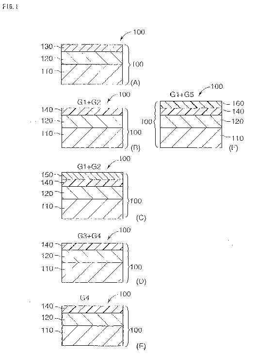
- Figs 1(A), 1(B), 1(C), 1(D), 1(E) and 1(F) are schematic views showing the respective steps of a method for manufacturing a buried insulating layer-type semiconductor silicon carbide substrate according to an embodiment of the present invention
- Fig 2 is a schematic view of a manufacturing apparatus for manufacturing a buried insulating layer-type semiconductor silicon carbide substrate according to a manufacturing method for a buried insulating layer-type semiconductor silicon carbide substrate according to an embodiment of the present invention.
- the dimensions of the thicknesses of the respective layers in Fig 1 differ from the actual proportions for the purpose of convenience of illustration.
- Fig 1 specifies the surrounding gas in each step of the manufacturing method for a buried insulating layer-type semiconductor silicon carbide substrate.
- the manufacturing method for a buried insulating layer-type semiconductor silicon carbide substrate has: the first step of placing an SOI substrate 100 having a surface silicon layer 130 of which the film thickness is no greater than 10 nm and having a buried insulator layer 120 in a heating furnace 200 and increasing the temperature of the atmosphere within heating furnace 200 while supplying a mixed gas (G1+G2) of a hydrogen gas G1 and a hydrocarbon gas G2 into the above described heating furnace 200 and, thereby, of metamorphosing surface silicon layer 130 of the above described SOI substrate 100 into a single crystal silicon carbide thin film 140; the second step of depositing a carbon thin film 150 on the above described single crystal silicon carbide thin film 140 by excessively carrying out the above described first step; the third step of replacing the above described mixed gas (G1+G2) with an inert gas G4 wherein an oxygen gas G3 is mixed in a predetermined ratio and, after that, of heating the above described SOI substrate 100 up to 550°C, or higher,
- the above described SOI substrate 100 is gained, as shown in Fig 1(A), by forming a buried insulator layer 120 in a silicon layer 110 as a buried insulator and by forming a surface silicon layer 130 having a film thickness of no greater than 10 nm on this buried insulator layer 120.
- the crystal orientation in surface silicon layer 130 of this SOI substrate 100 is, for example, in the plane direction (111).
- the film thickness of surface silicon layer 130 of SOI substrate 100 is controlled according to a well-known method such that surface silicon layer 130 is oxidized and is etched by hydrofluoric acid, or the like, so that a desired thickness of the surface silicon layer remains
- an electrical furnace can be used as the above described heating furnace 200.
- one end of this heating furnace 200 has an opening through which an SOI substrate, or the like, is inserted into, or extracted from, the furnace while the other end is connected to an exhaust means 210 and a heating means 230 such as an electrical heater is installed around the furnace wall 220.
- a gas supply means 300 for supplying a variety of gases into the furnace is connected to this heating furnace 200. Then, the pressure inside of this heating furnace 200 is equal to atmospheric pressure.
- the above described gas supply means 300 has a hydrogen gas supply part 310 for supplying a hydrogen gas G1, a hydrocarbon gas supply part 320 for supplying a hydrocarbon gas G2, an oxygen gas supply part 330 for supplying an oxygen gas G3, an inert gas supply part 340 for supplying an argon gas as an inert gas G4 (including a pure inert gas), a silane-based gas supply part 350 for supplying a silane-based gas G5 and a switching valve 360 to which these gas supply parts 310 to 350 are connected,
- This gas supply means 300 is connected to the above described heating furnace 200 via a supply tube 370.
- the above described SOI substrate 100 is placed inside of heating furnace 200 and a mixed gas (G1+G2), wherein hydrocarbon gas G2 is mixed with hydrogen gas G1 so that the ratio of the hydrocarbon gas becomes 1 volume %, is supplied into heating furnace 200 in this first step.
- a mixed gas G1+G2
- hydrogen gas G1 so that the ratio of the hydrocarbon gas becomes 1 volume %
- the temperature of the atmosphere within heating furnace 200 is heated up to 1200°C to 1405°C.
- surface silicon layer 130 of SOI substrate 100 is metamorphosed to single crystal silicon carbide thin film 140. That is to say, surface silicon layer 130 of SOI substrate 100 is metamorphosed to single crystal silicon carbide thin film 140 in this first step.
- the above described single crystal silicon carbide thin film 140 is gained by metamorphoseing surface silicon layer 130 and, therefore, the film thickness of single crystal silicon carbide thin film 140 becomes equal to the film thickness of surface silicon layer 130. That is to say, the film thickness of single crystal silicon carbide thin film 140 can be arbitrarily controlled according to the film thickness of surface silicon layer 130 of SOI substrate 100.
- the above described hydrogen gas G1 is a carrier gas and propane gas is utilized as hydrocarbon gas G2.
- the amount of supply of hydrogen gas G1 from hydrogen gas supply part 310 is 1000cc/min, for example, the amount of supply of hydrocarbon gas G2 from hydrocarbon gas supply part 320 is adjusted to be 10cc/min.
- ⁇ Second Step> (see Fig 1(C))
- the above described first step is excessively carried out so that carbon thin film 150 is deposited on the above described single crystal silicon carbide thin film 140 in this second step.
- the above described carbon thin film 150 is deposited by continuing the above described first step for a period of time of, for example, from several minutes to several hours.
- mixed gas (G1+G2) of hydrocarbon gas G2 supplied from the above described hydrocarbon gas supply part 320 and of hydrogen gas G1 supplied from hydrogen gas supply part 310 is replaced with inert gas G4, wherein oxygen G3 is mixed in a predetermined ratio and, then, the above described SOI substrate 100 is heated up to no less than 550°C, for example, approximately 650°C so that the above described carbon thin film 150 is etched and removed.
- Argon gas for example, is used as the above described inert gas G4.
- oxygen gas G3 mixed with this inert gas G4 in the case that the amount of supply of inert gas G4 from inert gas supply part 340 is 1000cc/min, for example, the amount of supply of oxygen gas G3 from oxygen gas supply part 330 is adjusted to 100cc/min.
- SOI substrate 100 is heated up to approximately 650°C by means of heating means 230. This condition is maintained for a period of time of from several minutes to several hours.
- Carbon thin film 150 formed on the surface of SOI substrate 100 is changed to a carbon dioxide gas as a result of a chemical reaction of C + O 2 ⁇ CO 2 . Thereby, carbon thin film 150 is etched and removed. Here, this carbon dioxide gas is released to the outside of heating furnace 200 by means of exhaust means 210.
- this fourth step the above described inert gas G4, in which an oxygen gas is mixed, is replaced with a pure inert gas G4 in which no oxygen gas is mixed and the temperature of the atmosphere within the above described heating furnace 200 is increased up to a predetermined temperature.
- a pure argon gas is utilized as the above described pure inert gas G4.
- a purpose of the replacement of the gas within heating furnace 200 with pure inert gas G4 in this fourth step is to avoid the risk of an explosive reaction of a methyl silane gas with an oxygen gas when silane-based gas G5 is utilized in the, subsequent, fifth step.
- the above described pure inert gas G4 is supplied to heating furnace 200 by stopping the supply of oxygen gas G3 that has been supplied to heating furnace 200 in the above described third step and by continuing the supply of inert gas G4.
- hydrogen gas G1 is supplied from hydrogen gas supply part 310 into heating furnace 200 and silane-based gas G5 is supplied from silane-based gas supply part 350 into heating furnace 200, respectively, under the condition wherein the above described predetermined temperature (500°C to 1405°C) of the atmosphere is maintained so that new single crystal silicon carbide thin film 160 is made to grow on single crystal silicon carbide thin film 140 on the surface of the above described SOI substrate 100.
- predetermined temperature 500°C to 1405°C
- silane-based gas G5 for example, a methyl silane gas is used. Silicon is generated as a result of decomposition of this methyl silane gas and is reacted with carbon in single crystal silicon carbide thin film 140 and, thereby, an additional single crystal silicon carbide thin film 160 is formed on single crystal silicon carbide thin film 140.
- silane-based gas G5 a monosilane gas, a disilane gas, a dimethylsilane gas, a dichlorosilane gas, or the like, in addition to the methyl silane gas can be utilized.
- a buried insulating layer-type semiconductor silicon carbide substrate having single crystal silicon carbide thin films 140 and 160 can be manufactured in the above described manner.
- mixed gas (G1+G2) required for the first step may be prepared in advance by mixing hydrogen gas G1 and hydrocarbon gas G2 in a predetermined ratio
- the mixed gas required for the third step may be prepared in advance by mixing inert gas G4 and oxygen gas G3 in a predetermined ratio
- the hydrogen gas and silane-based gas required for the fifth step may be mixed in advance in a predetermined ratio.
- the type of system wherein a variety of gases are separately supplied is more flexible, from a point of view of the feasibility of altering the mixture ratio of the various gases in order to cope with a variety of chemical reactions, than the type of system wherein a mixed gas prepared in advance by mixing a variety of gases in a predetermined ratio is supplied.
- the manufacturing method for a buried insulating layer-type semiconductor silicon carbide substrate according to the present invention has the step of placing an SOI substrate, having a surface silicon layer of which the film thickness is no greater than 10nm and having a buried insulator, in a heating furnace and of increasing the temperature of the atmosphere within the heating furnace while supplying a mixed gas of a hydrogen gas and of a hydrocarbon gas into the above described heating furnace so that the surface silicon layer of the above described SOI substrate is metamorphosed into a single crystal silicon carbide thin film.
- a single crystal silicon carbide thin film can be formed directly above a buried oxide layer according to this manufacturing method without an intervention of a silicon layer, which has caused a problem in a conventional plasma-type vapor phase reaction method, or the like, between the single crystal silicon carbide thin film and the buried oxide layer. Therefore, a buried insulating layer-type semiconductor silicon carbide substrate manufactured according to this manufacturing method solves the conventional problems such as occurrence of a variety of defects, and a coarse interface, in the interface between the single crystal silicon carbide thin film and the silicon layer located beneath the single crystal silicon carbide thin film.
- this manufacturing method solely requires a simple heating furnace, such as an electrical furnace, and it is not necessary to maintain a high vacuum as in the prior art and, therefore, this manufacturing method can contribute to the simplification of the manufacturing apparatus and of the manufacturing process and, as a result, can contribute to reduction in manufacturing costs.
- the film thickness of the surface silicon layer is no greater than 10nm, unlike the case of a film thickness of no less than 10nm, a coarse surface due to the occurrence of grains caused by local nucleus growth in single crystal silicon carbide is eliminated, so that an excellent surface condition can be gained.
- Figs 1(A) to 1(F) are schematic views showing the respective steps of the manufacturing method for a buried insulating layer-type semiconductor silicon carbide substrate according to an embodiment of the present invention.
- Fig 2 is a schematic view of a manufacturing apparatus for manufacturing a buried insulating layer semiconductor silicon carbide substrate for carrying out a manufacturing method for a buried insulating layer semiconductor silicon carbide substrate according to an embodiment of the present invention.
Landscapes
- Business, Economics & Management (AREA)
- Engineering & Computer Science (AREA)
- Health & Medical Sciences (AREA)
- Economics (AREA)
- Theoretical Computer Science (AREA)
- Finance (AREA)
- General Health & Medical Sciences (AREA)
- Accounting & Taxation (AREA)
- Primary Health Care (AREA)
- General Physics & Mathematics (AREA)
- General Business, Economics & Management (AREA)
- Tourism & Hospitality (AREA)
- Physics & Mathematics (AREA)
- Strategic Management (AREA)
- Marketing (AREA)
- Human Resources & Organizations (AREA)
- Life Sciences & Earth Sciences (AREA)
- Biophysics (AREA)
- Public Health (AREA)
- Physical Education & Sports Medicine (AREA)
- Medical Informatics (AREA)
- Epidemiology (AREA)
- Development Economics (AREA)
- Recrystallisation Techniques (AREA)
- Thin Film Transistor (AREA)
- Crystals, And After-Treatments Of Crystals (AREA)
Abstract
Description
- 100
- SOI substrate
- 110
- silicon layer
- 120
- buried insulator layer
- 130
- surface silicon layer
- 140
- single crystal silicon carbide thin film
- 150
- carbon thin film
- 160
- single crystal silicon carbide thin film
Claims (9)
- A manufacturing method for a buried insulating layer-type semiconductor silicon carbide substrate, characterized in comprising the step of placing an SOI substrate, which has a surface silicon layer of a predetermined thickness and a buried insulator, in a heating furnace and of increasing the temperature of the atmosphere within the heating furnace while supplying a mixed gas of a hydrogen gas and of a hydrocarbon gas into said heating furnace and, thereby, of metamorphosing the surface silicon layer of said SOI substrate into a single crystal silicon carbide thin film.
- A manufacturing method for a buried insulating layer-type semiconductor silicon carbide substrate, characterized in comprising: the first step of placing an SOI substrate, which has a surface silicon layer of a predetermined thickness and a buried insulator, in a heating furnace and of increasing the temperature of the atmosphere within the heating furnace while supplying a mixed gas of a hydrogen gas and of a hydrocarbon gas into said heating furnace and, thereby, of metamorphosing the surface silicon layer of said SOI substrate into a single crystal silicon carbide thin film; the second step of depositing a carbon thin film on said single crystal silicon carbide thin film by excessively carrying out said first step; the third step of replacing said mixed gas with an inert gas wherein an oxygen gas is mixed in a predetermined ratio and of heating said SOI substrate up to 550°C, or higher, so that said carbon thin film is removed through etching; the fourth step of replacing said inert gas wherein an oxygen gas is mixed with a pure inert gas into which no oxygen gas is mixed and of increasing the temperature of the atmosphere within said heating furnace up to a predetermined temperature; and the fifth step of making a new single crystal silicon carbide thin film grow on the single crystal silicon carbide thin film on the surface of said SOI substrate by supplying a hydrogen gas and a silane-based gas into the heating furnace under the condition wherein said predetermined temperature of the atmosphere is maintained.
- A method according to claim 2, wherein said predetermined temperature is in a range of from 500°C to 1405°C.
- A method according to any preceding claim, wherein the surface silicon layer of said predetermined thickness has a film thickness of 10 nm, or less.
- A method according to any preceeding claim, wherein said sequential reactions are carried out under an atmospheric pressure.
- Apparatus for manufacturing a buried insulating layer-type semiconductor silicon carbide substrate, comprising:characterized in that said gas supply means (300) can supply, at least, a hydrogen gas (G1), a hydrocarbon gas (G2), an oxygen gas (G3), an inert gas (G4) and a silane-based gas (G5) into the heating furnace.a heating furnace (200) adapted to receive an SOI substrate (100) of the type having a surface silicon layer (130) of a predetermined thickness and a buried insulator (120);heating means (230) for heating the SOI substrate; anda gas supply means (300) for supplying a variety of gases into heating furnace (200);
- Apparatus according to claim 6, wherein the inside of said heating furnace is at atmospheric pressure.
- A method for manufacturing a buried insulating layer-type semiconductor silicon carbide substrate (100), comprising placing in a heating furnace (200) an SOI substrate having a surface silicon layer (130) of a predetermined thickness and a buried insulator (120), and increasing the temperature of the atmosphere within the heating furnace; characterised in that said step of increasing the temperature is conducted while supplying a mixture of hydrogen gas (G1) and hydrocarbon gas (G2) into said heating furnace whereby said surface silicon layer is metamorphosed into a single crystal silicon carbide thin film (140).
- A method according to claim 8 comprising the further steps of:depositing a carbon thin film on said single crystal silicon carbide thin film by excessively carrying out said metamorphasing step;replacing said mixed gas with an inert gas in which oxygen gas is mixed in a predetermined ratio and heating said SOI substrate up to 550°C, or higher, so that said carbon thin film is removed through etching;
replacing said inert gas in which oxygen gas is mixed with a pure inert gas in which no oxygen gas is mixed and increasing the temperature of the atmosphere within said heating furnace up to a predetermined temperature; andgrowing a new single crystal silicon carbide thin film on the single crystal silicon carbide thin film on the surface of said SOI substrate by supplying hydrogen gas and a silane-based gas into the heating furnace under conditions wherein said predetermined temperature of the atmosphere is maintained.
Applications Claiming Priority (2)
| Application Number | Priority Date | Filing Date | Title |
|---|---|---|---|
| JP2002022631 | 2002-01-31 | ||
| JP2002022631A JP3920103B2 (en) | 2002-01-31 | 2002-01-31 | Insulating layer embedded type semiconductor silicon carbide substrate manufacturing method and manufacturing apparatus thereof |
Publications (3)
| Publication Number | Publication Date |
|---|---|
| EP1333482A2 true EP1333482A2 (en) | 2003-08-06 |
| EP1333482A3 EP1333482A3 (en) | 2006-02-01 |
| EP1333482B1 EP1333482B1 (en) | 2008-06-25 |
Family
ID=19192223
Family Applications (1)
| Application Number | Title | Priority Date | Filing Date |
|---|---|---|---|
| EP03250583A Expired - Lifetime EP1333482B1 (en) | 2002-01-31 | 2003-01-30 | Method for manufacturing a semiconductor silicon carbide on insulator substrate (SOI) and apparatus therefore |
Country Status (7)
| Country | Link |
|---|---|
| US (2) | US7084049B2 (en) |
| EP (1) | EP1333482B1 (en) |
| JP (1) | JP3920103B2 (en) |
| KR (1) | KR100777544B1 (en) |
| CN (1) | CN100343962C (en) |
| DE (1) | DE60321734D1 (en) |
| TW (1) | TWI264070B (en) |
Cited By (3)
| Publication number | Priority date | Publication date | Assignee | Title |
|---|---|---|---|---|
| CN102965733A (en) * | 2012-11-02 | 2013-03-13 | 中国科学院物理研究所 | Growth technique of graphite-coating-free conductive silicon carbide crystals |
| MD4280C1 (en) * | 2013-09-04 | 2014-10-31 | Государственный Университет Молд0 | pInP-nCdS structure growth method |
| MD4554B1 (en) * | 2017-10-18 | 2018-02-28 | Государственный Университет Молд0 | Process for increasing the efficiency of photovoltaic cells based on p+InP-p-InP-n+CdS |
Families Citing this family (19)
| Publication number | Priority date | Publication date | Assignee | Title |
|---|---|---|---|---|
| JP2002280354A (en) * | 2001-03-19 | 2002-09-27 | Osaka Prefecture | Method and apparatus for etching carbon thin film |
| US7147715B2 (en) * | 2003-07-28 | 2006-12-12 | Cree, Inc. | Growth of ultra-high purity silicon carbide crystals in an ambient containing hydrogen |
| US20070231485A1 (en) * | 2003-09-05 | 2007-10-04 | Moffat William A | Silane process chamber with double door seal |
| US7382023B2 (en) * | 2004-04-28 | 2008-06-03 | Taiwan Semiconductor Manufacturing Company, Ltd. | Fully depleted SOI multiple threshold voltage application |
| JP2005317801A (en) * | 2004-04-28 | 2005-11-10 | Japan Science & Technology Agency | Thin film element formation method |
| JP4690734B2 (en) * | 2005-01-28 | 2011-06-01 | エア・ウォーター株式会社 | Method for producing single crystal SiC substrate |
| JP4511378B2 (en) * | 2005-02-15 | 2010-07-28 | エア・ウォーター株式会社 | Method for forming single crystal SiC layer using SOI substrate |
| JP4563918B2 (en) * | 2005-10-31 | 2010-10-20 | エア・ウォーター株式会社 | Method for producing single crystal SiC substrate |
| CN100514562C (en) * | 2006-09-18 | 2009-07-15 | 中国科学院半导体研究所 | Making method for large-area 3C-SiC thin film of MEMS part |
| WO2008111277A1 (en) * | 2007-03-15 | 2008-09-18 | Kyushu Institute Of Technology | Single crystal zinc oxide substrate |
| JP5394632B2 (en) | 2007-11-19 | 2014-01-22 | エア・ウォーター株式会社 | Method for producing single crystal SiC substrate |
| JP2009158702A (en) * | 2007-12-26 | 2009-07-16 | Kyushu Institute Of Technology | Light emitting device |
| US20110117372A1 (en) * | 2008-03-10 | 2011-05-19 | Tohoku University | Graphene or graphite thin film, manufacturing method thereof, thin film structure and electronic device |
| JP2011243640A (en) * | 2010-05-14 | 2011-12-01 | Sumitomo Electric Ind Ltd | Manufacturing method of silicon carbide substrate, manufacturing method of semiconductor device, silicon carbide substrate, and semiconductor device |
| JP5585268B2 (en) | 2010-07-22 | 2014-09-10 | セイコーエプソン株式会社 | SUBSTRATE WITH SINGLE CRYSTAL SILICON CARBIDE FILM, METHOD FOR PRODUCING SINGLE CRYSTAL SILICON CARBIDE CARBON FILM, AND METHOD FOR MANUFACTURING SUBSTRATE WITH SINGLE CRYSTAL SILICON CARBIDE CARBIDE FILM |
| JP6111678B2 (en) * | 2013-01-17 | 2017-04-12 | 信越半導体株式会社 | Manufacturing method of GeOI wafer |
| JP6136731B2 (en) * | 2013-08-06 | 2017-05-31 | 住友電気工業株式会社 | Silicon carbide semiconductor substrate, method of manufacturing the same, and method of manufacturing silicon carbide semiconductor device |
| JPWO2016047534A1 (en) * | 2014-09-24 | 2017-07-27 | エア・ウォーター株式会社 | Semiconductor device provided with SiC layer |
| RU2578104C1 (en) * | 2015-04-07 | 2016-03-20 | Федеральное государственное автономное образовательное учреждение высшего образования "Национальный исследовательский университет "Московский институт электронной техники" (МИЭТ) | Method for gas-phase carbidisation of surface of monocrystalline silicon of orientation (111), (100) |
Family Cites Families (8)
| Publication number | Priority date | Publication date | Assignee | Title |
|---|---|---|---|---|
| US4664944A (en) * | 1986-01-31 | 1987-05-12 | The United States Of America As Represented By The United States Department Of Energy | Deposition method for producing silicon carbide high-temperature semiconductors |
| JP2962851B2 (en) * | 1990-04-26 | 1999-10-12 | キヤノン株式会社 | Light receiving member |
| JPH06191997A (en) | 1992-10-07 | 1994-07-12 | Kyushu Kogyo Univ | Method of forming SiC crystal film |
| US5415126A (en) * | 1993-08-16 | 1995-05-16 | Dow Corning Corporation | Method of forming crystalline silicon carbide coatings at low temperatures |
| DE19514079A1 (en) * | 1995-04-13 | 1996-10-17 | Siemens Ag | Process for passivating a silicon carbide surface against oxygen |
| US5759908A (en) * | 1995-05-16 | 1998-06-02 | University Of Cincinnati | Method for forming SiC-SOI structures |
| US5880491A (en) * | 1997-01-31 | 1999-03-09 | The United States Of America As Represented By The Secretary Of The Air Force | SiC/111-V-nitride heterostructures on SiC/SiO2 /Si for optoelectronic devices |
| JP2002363751A (en) * | 2001-06-06 | 2002-12-18 | Osaka Prefecture | Method and apparatus for manufacturing single crystal silicon carbide thin film |
-
2002
- 2002-01-31 JP JP2002022631A patent/JP3920103B2/en not_active Expired - Lifetime
- 2002-12-27 TW TW091137731A patent/TWI264070B/en not_active IP Right Cessation
-
2003
- 2003-01-16 KR KR1020030002943A patent/KR100777544B1/en not_active Expired - Fee Related
- 2003-01-27 CN CNB031034705A patent/CN100343962C/en not_active Expired - Lifetime
- 2003-01-27 US US10/351,385 patent/US7084049B2/en not_active Expired - Lifetime
- 2003-01-30 EP EP03250583A patent/EP1333482B1/en not_active Expired - Lifetime
- 2003-01-30 DE DE60321734T patent/DE60321734D1/en not_active Expired - Lifetime
-
2004
- 2004-03-18 US US10/802,806 patent/US7128788B2/en not_active Expired - Lifetime
Cited By (4)
| Publication number | Priority date | Publication date | Assignee | Title |
|---|---|---|---|---|
| CN102965733A (en) * | 2012-11-02 | 2013-03-13 | 中国科学院物理研究所 | Growth technique of graphite-coating-free conductive silicon carbide crystals |
| CN102965733B (en) * | 2012-11-02 | 2015-11-18 | 中国科学院物理研究所 | A kind of conductive carbonized silicon crystal growing process without graphite wrap |
| MD4280C1 (en) * | 2013-09-04 | 2014-10-31 | Государственный Университет Молд0 | pInP-nCdS structure growth method |
| MD4554B1 (en) * | 2017-10-18 | 2018-02-28 | Государственный Университет Молд0 | Process for increasing the efficiency of photovoltaic cells based on p+InP-p-InP-n+CdS |
Also Published As
| Publication number | Publication date |
|---|---|
| US7084049B2 (en) | 2006-08-01 |
| KR100777544B1 (en) | 2007-11-20 |
| TW200306627A (en) | 2003-11-16 |
| US20040173154A1 (en) | 2004-09-09 |
| EP1333482A3 (en) | 2006-02-01 |
| CN100343962C (en) | 2007-10-17 |
| JP2003224248A (en) | 2003-08-08 |
| EP1333482B1 (en) | 2008-06-25 |
| US20030148586A1 (en) | 2003-08-07 |
| TWI264070B (en) | 2006-10-11 |
| DE60321734D1 (en) | 2008-08-07 |
| JP3920103B2 (en) | 2007-05-30 |
| KR20030065326A (en) | 2003-08-06 |
| CN1435866A (en) | 2003-08-13 |
| US7128788B2 (en) | 2006-10-31 |
Similar Documents
| Publication | Publication Date | Title |
|---|---|---|
| US7084049B2 (en) | Manufacturing method for buried insulating layer-type semiconductor silicon carbide substrate | |
| US6056820A (en) | Advanced physical vapor transport method and apparatus for growing high purity single crystal silicon carbide | |
| JPS6344718A (en) | Manufacture of crystalline deposited | |
| CA2583683C (en) | Surface reconstruction method for silicon carbide substrate | |
| JP2014058411A (en) | Method for producing epitaxial silicon carbide wafer | |
| CN100380586C (en) | Manufacturing method and manufacturing equipment of single crystal silicon carbide thin film | |
| WO2009066566A1 (en) | PROCESS FOR PRODUCING SINGLE CRYSTAL SiC SUBSTRATE AND SINGLE CRYSTAL SiC SUBSTRATE PRODUCED BY THE PROCESS | |
| EP0241204B1 (en) | Method for forming crystalline deposited film | |
| US7919397B2 (en) | Method for reducing agglomeration of Si layer, method for manufacturing semiconductor device and vacuum treatment apparatus | |
| WO2002000968A1 (en) | A method for manufacturing a susceptor, a susceptor thus obtained and its application | |
| WO2005087983A2 (en) | Alternative methods for fabrication of substrates and heterostructures made of silicon compounds and alloys | |
| JP3344205B2 (en) | Method for manufacturing silicon wafer and silicon wafer | |
| JPS60145376A (en) | Growing method of tungsten silicide film | |
| US9945048B2 (en) | Semiconductor structure and method | |
| JPH06333822A (en) | Semiconductor device | |
| JP3194547B2 (en) | Method for manufacturing polycrystalline silicon layer | |
| US20240166516A1 (en) | Method of manufacturing hexagonal boron nitride multilayer | |
| US20070254451A1 (en) | Process for forming a silicon-based single-crystal portion | |
| JP2003528443A5 (en) | ||
| JPS59177919A (en) | Selective growth of thin film | |
| KR100233146B1 (en) | Method for fabricating polysilicon | |
| JPS6253933B2 (en) | ||
| JP2004186376A (en) | Apparatus and method for manufacturing silicon wafer | |
| JPS61131434A (en) | Manufacture of semiconductor device | |
| JPH0974055A (en) | Composite semiconductor substrate |
Legal Events
| Date | Code | Title | Description |
|---|---|---|---|
| PUAI | Public reference made under article 153(3) epc to a published international application that has entered the european phase |
Free format text: ORIGINAL CODE: 0009012 |
|
| AK | Designated contracting states |
Designated state(s): AT BE BG CH CY CZ DE DK EE ES FI FR GB GR HU IE IT LI LU MC NL PT SE SI SK TR |
|
| AX | Request for extension of the european patent |
Extension state: AL LT LV MK RO |
|
| PUAL | Search report despatched |
Free format text: ORIGINAL CODE: 0009013 |
|
| AK | Designated contracting states |
Kind code of ref document: A3 Designated state(s): AT BE BG CH CY CZ DE DK EE ES FI FR GB GR HU IE IT LI LU MC NL PT SE SI SK TR |
|
| AX | Request for extension of the european patent |
Extension state: AL LT LV MK RO |
|
| 17P | Request for examination filed |
Effective date: 20060220 |
|
| AKX | Designation fees paid |
Designated state(s): DE FR GB NL |
|
| 17Q | First examination report despatched |
Effective date: 20070102 |
|
| GRAP | Despatch of communication of intention to grant a patent |
Free format text: ORIGINAL CODE: EPIDOSNIGR1 |
|
| GRAS | Grant fee paid |
Free format text: ORIGINAL CODE: EPIDOSNIGR3 |
|
| GRAA | (expected) grant |
Free format text: ORIGINAL CODE: 0009210 |
|
| AK | Designated contracting states |
Kind code of ref document: B1 Designated state(s): DE FR GB NL |
|
| REG | Reference to a national code |
Ref country code: GB Ref legal event code: FG4D |
|
| REF | Corresponds to: |
Ref document number: 60321734 Country of ref document: DE Date of ref document: 20080807 Kind code of ref document: P |
|
| RAP2 | Party data changed (patent owner data changed or rights of a patent transferred) |
Owner name: OSAKA PREFECTURE UNIVERSITY PUBLIC CORPORATION |
|
| PLBE | No opposition filed within time limit |
Free format text: ORIGINAL CODE: 0009261 |
|
| STAA | Information on the status of an ep patent application or granted ep patent |
Free format text: STATUS: NO OPPOSITION FILED WITHIN TIME LIMIT |
|
| REG | Reference to a national code |
Ref country code: GB Ref legal event code: 732E Free format text: REGISTERED BETWEEN 20090416 AND 20090422 |
|
| NLT2 | Nl: modifications (of names), taken from the european patent patent bulletin |
Owner name: OSAKA PREFECTURE UNIVERSITY PUBLIC CORPORATION Effective date: 20090415 |
|
| 26N | No opposition filed |
Effective date: 20090326 |
|
| NLS | Nl: assignments of ep-patents |
Owner name: OSAKA PREFECTURE UNIVERSITY PUBLIC CORPORATION Effective date: 20090420 |
|
| REG | Reference to a national code |
Ref country code: FR Ref legal event code: TP |
|
| REG | Reference to a national code |
Ref country code: DE Ref legal event code: R082 Ref document number: 60321734 Country of ref document: DE Representative=s name: STREHL, SCHUEBEL-HOPF & PARTNER, DE |
|
| REG | Reference to a national code |
Ref country code: DE Ref legal event code: R081 Ref document number: 60321734 Country of ref document: DE Owner name: OSAKA PREFECTURE UNIVERSITY PUBLIC CORP., JP Free format text: FORMER OWNER: OSAKA PREFECTURE UNIVERSITY PUBLIC CORP., SAKAI, JP Effective date: 20130611 Ref country code: DE Ref legal event code: R082 Ref document number: 60321734 Country of ref document: DE Representative=s name: STREHL, SCHUEBEL-HOPF & PARTNER, DE Effective date: 20130611 Ref country code: DE Ref legal event code: R081 Ref document number: 60321734 Country of ref document: DE Owner name: AIR WATER INC., JP Free format text: FORMER OWNER: OSAKA PREFECTURE UNIVERSITY PUBLIC CORP., SAKAI, JP Effective date: 20130611 Ref country code: DE Ref legal event code: R082 Ref document number: 60321734 Country of ref document: DE Representative=s name: PATENTANWAELTE STREHL, SCHUEBEL-HOPF & PARTNER, DE Effective date: 20130611 Ref country code: DE Ref legal event code: R081 Ref document number: 60321734 Country of ref document: DE Owner name: AIR WATER INC., JP Free format text: FORMER OWNER: OSAKA PREFECTURE UNIVERSITY PUBLIC CORP., SAKAI-SHI, JP Effective date: 20130611 Ref country code: DE Ref legal event code: R081 Ref document number: 60321734 Country of ref document: DE Owner name: AIR WATER INC., SAPPORO, JP Free format text: FORMER OWNER: OSAKA PREFECTURE UNIVERSITY PUBLIC CORP., SAKAI-SHI, OSAKA, JP Effective date: 20130611 Ref country code: DE Ref legal event code: R082 Ref document number: 60321734 Country of ref document: DE Representative=s name: STREHL SCHUEBEL-HOPF & PARTNER MBB PATENTANWAE, DE Effective date: 20130611 |
|
| REG | Reference to a national code |
Ref country code: GB Ref legal event code: 732E Free format text: REGISTERED BETWEEN 20130808 AND 20130814 |
|
| REG | Reference to a national code |
Ref country code: FR Ref legal event code: TQ Owner name: AIR WATER INC., JP Effective date: 20130807 Ref country code: FR Ref legal event code: TQ Owner name: OSAKA PREFECTURE UNIVERSITY PUBLIC CORPORATION, JP Effective date: 20130807 |
|
| REG | Reference to a national code |
Ref country code: NL Ref legal event code: SD Effective date: 20130903 |
|
| REG | Reference to a national code |
Ref country code: DE Ref legal event code: R082 Ref document number: 60321734 Country of ref document: DE Representative=s name: PATENTANWAELTE STREHL, SCHUEBEL-HOPF & PARTNER, DE |
|
| REG | Reference to a national code |
Ref country code: GB Ref legal event code: 732E Free format text: REGISTERED BETWEEN 20140508 AND 20140514 |
|
| REG | Reference to a national code |
Ref country code: DE Ref legal event code: R081 Ref document number: 60321734 Country of ref document: DE Owner name: AIR WATER INC., JP Free format text: FORMER OWNER: AIR WATER INC., OSAKA PREFECTURE UNIVERSITY PUB, , JP Effective date: 20140429 Ref country code: DE Ref legal event code: R081 Ref document number: 60321734 Country of ref document: DE Owner name: AIR WATER INC., SAPPORO, JP Free format text: FORMER OWNER: AIR WATER INC., OSAKA PREFECTURE UNIVERSITY PUB, , JP Effective date: 20140429 Ref country code: DE Ref legal event code: R081 Ref document number: 60321734 Country of ref document: DE Owner name: AIR WATER INC., SAPPORO, JP Free format text: FORMER OWNERS: AIR WATER INC., SAPPORO, HOKKAIDO, JP; OSAKA PREFECTURE UNIVERSITY PUBLIC CORP., SAKAI-SHI, OSAKA, JP Effective date: 20140429 Ref country code: DE Ref legal event code: R082 Ref document number: 60321734 Country of ref document: DE Representative=s name: STREHL SCHUEBEL-HOPF & PARTNER MBB PATENTANWAE, DE Effective date: 20140429 Ref country code: DE Ref legal event code: R082 Ref document number: 60321734 Country of ref document: DE Representative=s name: PATENTANWAELTE STREHL, SCHUEBEL-HOPF & PARTNER, DE Effective date: 20140429 |
|
| REG | Reference to a national code |
Ref country code: FR Ref legal event code: TP Owner name: AIR WATER INC., JP Effective date: 20140519 |
|
| REG | Reference to a national code |
Ref country code: NL Ref legal event code: SD Effective date: 20141022 |
|
| REG | Reference to a national code |
Ref country code: FR Ref legal event code: PLFP Year of fee payment: 14 |
|
| REG | Reference to a national code |
Ref country code: FR Ref legal event code: PLFP Year of fee payment: 15 |
|
| REG | Reference to a national code |
Ref country code: FR Ref legal event code: PLFP Year of fee payment: 16 |
|
| PGFP | Annual fee paid to national office [announced via postgrant information from national office to epo] |
Ref country code: GB Payment date: 20211209 Year of fee payment: 20 Ref country code: FR Payment date: 20211217 Year of fee payment: 20 |
|
| PGFP | Annual fee paid to national office [announced via postgrant information from national office to epo] |
Ref country code: NL Payment date: 20211216 Year of fee payment: 20 |
|
| PGFP | Annual fee paid to national office [announced via postgrant information from national office to epo] |
Ref country code: DE Payment date: 20211207 Year of fee payment: 20 |
|
| REG | Reference to a national code |
Ref country code: DE Ref legal event code: R071 Ref document number: 60321734 Country of ref document: DE |
|
| REG | Reference to a national code |
Ref country code: NL Ref legal event code: MK Effective date: 20230129 |
|
| REG | Reference to a national code |
Ref country code: GB Ref legal event code: PE20 Expiry date: 20230129 |
|
| PG25 | Lapsed in a contracting state [announced via postgrant information from national office to epo] |
Ref country code: GB Free format text: LAPSE BECAUSE OF EXPIRATION OF PROTECTION Effective date: 20230129 |