EP1330642B1 - Verfahren zur modifizierung von silber-elektroden mittels eines chlorplasmas - Google Patents
Verfahren zur modifizierung von silber-elektroden mittels eines chlorplasmas Download PDFInfo
- Publication number
- EP1330642B1 EP1330642B1 EP01980648A EP01980648A EP1330642B1 EP 1330642 B1 EP1330642 B1 EP 1330642B1 EP 01980648 A EP01980648 A EP 01980648A EP 01980648 A EP01980648 A EP 01980648A EP 1330642 B1 EP1330642 B1 EP 1330642B1
- Authority
- EP
- European Patent Office
- Prior art keywords
- silver
- plasma
- electrode
- chlorine
- layer
- Prior art date
- Legal status (The legal status is an assumption and is not a legal conclusion. Google has not performed a legal analysis and makes no representation as to the accuracy of the status listed.)
- Expired - Lifetime
Links
- 229910052709 silver Inorganic materials 0.000 title claims abstract description 86
- 239000004332 silver Substances 0.000 title claims abstract description 86
- BQCADISMDOOEFD-UHFFFAOYSA-N Silver Chemical compound [Ag] BQCADISMDOOEFD-UHFFFAOYSA-N 0.000 title claims abstract description 79
- 238000000034 method Methods 0.000 title claims abstract description 35
- 239000000460 chlorine Substances 0.000 title claims abstract description 30
- 229910052801 chlorine Inorganic materials 0.000 title claims abstract description 24
- ZAMOUSCENKQFHK-UHFFFAOYSA-N Chlorine atom Chemical compound [Cl] ZAMOUSCENKQFHK-UHFFFAOYSA-N 0.000 title claims abstract description 22
- 238000012986 modification Methods 0.000 title claims abstract description 16
- 230000004048 modification Effects 0.000 title claims abstract description 16
- 239000010409 thin film Substances 0.000 claims abstract description 23
- 230000004907 flux Effects 0.000 claims abstract description 4
- 229910052751 metal Inorganic materials 0.000 claims abstract description 4
- 239000002184 metal Substances 0.000 claims abstract description 4
- HKZLPVFGJNLROG-UHFFFAOYSA-M silver monochloride Chemical compound [Cl-].[Ag+] HKZLPVFGJNLROG-UHFFFAOYSA-M 0.000 claims description 40
- 229910021607 Silver chloride Inorganic materials 0.000 claims description 38
- 239000010410 layer Substances 0.000 claims description 26
- 239000011521 glass Substances 0.000 claims description 11
- 238000001704 evaporation Methods 0.000 claims description 8
- 230000008020 evaporation Effects 0.000 claims description 7
- 238000004544 sputter deposition Methods 0.000 claims description 6
- VYZAMTAEIAYCRO-UHFFFAOYSA-N Chromium Chemical group [Cr] VYZAMTAEIAYCRO-UHFFFAOYSA-N 0.000 claims description 5
- 238000006243 chemical reaction Methods 0.000 claims description 5
- 229910052804 chromium Inorganic materials 0.000 claims description 5
- 239000011651 chromium Substances 0.000 claims description 5
- 238000000992 sputter etching Methods 0.000 claims description 4
- 229910001120 nichrome Inorganic materials 0.000 claims description 2
- 150000003378 silver Chemical class 0.000 claims description 2
- 239000002344 surface layer Substances 0.000 claims description 2
- 238000005259 measurement Methods 0.000 abstract description 6
- 125000001309 chloro group Chemical group Cl* 0.000 abstract description 5
- 150000002500 ions Chemical class 0.000 abstract description 3
- 239000007943 implant Substances 0.000 abstract description 2
- 210000002381 plasma Anatomy 0.000 description 37
- -1 silver halide Chemical class 0.000 description 10
- 239000010408 film Substances 0.000 description 8
- 238000004626 scanning electron microscopy Methods 0.000 description 8
- 238000011282 treatment Methods 0.000 description 8
- WCUXLLCKKVVCTQ-UHFFFAOYSA-M Potassium chloride Chemical compound [Cl-].[K+] WCUXLLCKKVVCTQ-UHFFFAOYSA-M 0.000 description 7
- VEXZGXHMUGYJMC-UHFFFAOYSA-M Chloride anion Chemical compound [Cl-] VEXZGXHMUGYJMC-UHFFFAOYSA-M 0.000 description 6
- 238000004833 X-ray photoelectron spectroscopy Methods 0.000 description 6
- 238000002149 energy-dispersive X-ray emission spectroscopy Methods 0.000 description 6
- 238000012360 testing method Methods 0.000 description 5
- XKRFYHLGVUSROY-UHFFFAOYSA-N Argon Chemical compound [Ar] XKRFYHLGVUSROY-UHFFFAOYSA-N 0.000 description 4
- VEXZGXHMUGYJMC-UHFFFAOYSA-N Hydrochloric acid Chemical group Cl VEXZGXHMUGYJMC-UHFFFAOYSA-N 0.000 description 4
- 150000001875 compounds Chemical class 0.000 description 4
- 239000003792 electrolyte Substances 0.000 description 4
- 238000005516 engineering process Methods 0.000 description 4
- 239000000126 substance Substances 0.000 description 4
- FAPWRFPIFSIZLT-UHFFFAOYSA-M Sodium chloride Chemical compound [Na+].[Cl-] FAPWRFPIFSIZLT-UHFFFAOYSA-M 0.000 description 3
- 238000009713 electroplating Methods 0.000 description 3
- 229910001385 heavy metal Inorganic materials 0.000 description 3
- 238000001453 impedance spectrum Methods 0.000 description 3
- 230000001590 oxidative effect Effects 0.000 description 3
- 239000001103 potassium chloride Substances 0.000 description 3
- 235000011164 potassium chloride Nutrition 0.000 description 3
- 230000009467 reduction Effects 0.000 description 3
- 239000000243 solution Substances 0.000 description 3
- 239000003513 alkali Substances 0.000 description 2
- 238000004458 analytical method Methods 0.000 description 2
- 229910052786 argon Inorganic materials 0.000 description 2
- 230000015572 biosynthetic process Effects 0.000 description 2
- 238000000840 electrochemical analysis Methods 0.000 description 2
- 150000004820 halides Chemical class 0.000 description 2
- 238000011835 investigation Methods 0.000 description 2
- 239000002245 particle Substances 0.000 description 2
- 239000008055 phosphate buffer solution Substances 0.000 description 2
- 230000008569 process Effects 0.000 description 2
- 230000035945 sensitivity Effects 0.000 description 2
- 238000001228 spectrum Methods 0.000 description 2
- ABEXEQSGABRUHS-UHFFFAOYSA-N 16-methylheptadecyl 16-methylheptadecanoate Chemical compound CC(C)CCCCCCCCCCCCCCCOC(=O)CCCCCCCCCCCCCCC(C)C ABEXEQSGABRUHS-UHFFFAOYSA-N 0.000 description 1
- 235000011299 Brassica oleracea var botrytis Nutrition 0.000 description 1
- 240000003259 Brassica oleracea var. botrytis Species 0.000 description 1
- OKTJSMMVPCPJKN-UHFFFAOYSA-N Carbon Chemical compound [C] OKTJSMMVPCPJKN-UHFFFAOYSA-N 0.000 description 1
- KZBUYRJDOAKODT-UHFFFAOYSA-N Chlorine Chemical compound ClCl KZBUYRJDOAKODT-UHFFFAOYSA-N 0.000 description 1
- 241000160765 Erebia ligea Species 0.000 description 1
- PXGOKWXKJXAPGV-UHFFFAOYSA-N Fluorine Chemical compound FF PXGOKWXKJXAPGV-UHFFFAOYSA-N 0.000 description 1
- 241000764238 Isis Species 0.000 description 1
- 240000007594 Oryza sativa Species 0.000 description 1
- 235000007164 Oryza sativa Nutrition 0.000 description 1
- 238000000026 X-ray photoelectron spectrum Methods 0.000 description 1
- 238000010521 absorption reaction Methods 0.000 description 1
- QVGXLLKOCUKJST-UHFFFAOYSA-N atomic oxygen Chemical compound [O] QVGXLLKOCUKJST-UHFFFAOYSA-N 0.000 description 1
- 229910052799 carbon Inorganic materials 0.000 description 1
- 210000004027 cell Anatomy 0.000 description 1
- 150000001805 chlorine compounds Chemical class 0.000 description 1
- 239000000356 contaminant Substances 0.000 description 1
- 238000005336 cracking Methods 0.000 description 1
- 238000000151 deposition Methods 0.000 description 1
- 238000009826 distribution Methods 0.000 description 1
- 238000002848 electrochemical method Methods 0.000 description 1
- 230000005518 electrochemistry Effects 0.000 description 1
- 238000010894 electron beam technology Methods 0.000 description 1
- 238000005530 etching Methods 0.000 description 1
- 238000002474 experimental method Methods 0.000 description 1
- 239000010419 fine particle Substances 0.000 description 1
- 229910052731 fluorine Inorganic materials 0.000 description 1
- 239000011737 fluorine Substances 0.000 description 1
- 239000007789 gas Substances 0.000 description 1
- 239000008187 granular material Substances 0.000 description 1
- 238000005417 image-selected in vivo spectroscopy Methods 0.000 description 1
- 239000000976 ink Substances 0.000 description 1
- 238000012739 integrated shape imaging system Methods 0.000 description 1
- 239000000463 material Substances 0.000 description 1
- 239000000203 mixture Substances 0.000 description 1
- 229910052755 nonmetal Inorganic materials 0.000 description 1
- 230000003287 optical effect Effects 0.000 description 1
- 230000003647 oxidation Effects 0.000 description 1
- 238000007254 oxidation reaction Methods 0.000 description 1
- 239000001301 oxygen Substances 0.000 description 1
- 229910052760 oxygen Inorganic materials 0.000 description 1
- 238000009832 plasma treatment Methods 0.000 description 1
- 229920000642 polymer Polymers 0.000 description 1
- 238000011002 quantification Methods 0.000 description 1
- 230000004044 response Effects 0.000 description 1
- 235000009566 rice Nutrition 0.000 description 1
- 238000007788 roughening Methods 0.000 description 1
- 238000000550 scanning electron microscopy energy dispersive X-ray spectroscopy Methods 0.000 description 1
- 239000011780 sodium chloride Substances 0.000 description 1
- 241000894007 species Species 0.000 description 1
- 238000012876 topography Methods 0.000 description 1
- 238000012546 transfer Methods 0.000 description 1
Images


Classifications
-
- G—PHYSICS
- G01—MEASURING; TESTING
- G01N—INVESTIGATING OR ANALYSING MATERIALS BY DETERMINING THEIR CHEMICAL OR PHYSICAL PROPERTIES
- G01N27/00—Investigating or analysing materials by the use of electric, electrochemical, or magnetic means
- G01N27/26—Investigating or analysing materials by the use of electric, electrochemical, or magnetic means by investigating electrochemical variables; by using electrolysis or electrophoresis
- G01N27/28—Electrolytic cell components
- G01N27/30—Electrodes, e.g. test electrodes; Half-cells
-
- C—CHEMISTRY; METALLURGY
- C23—COATING METALLIC MATERIAL; COATING MATERIAL WITH METALLIC MATERIAL; CHEMICAL SURFACE TREATMENT; DIFFUSION TREATMENT OF METALLIC MATERIAL; COATING BY VACUUM EVAPORATION, BY SPUTTERING, BY ION IMPLANTATION OR BY CHEMICAL VAPOUR DEPOSITION, IN GENERAL; INHIBITING CORROSION OF METALLIC MATERIAL OR INCRUSTATION IN GENERAL
- C23C—COATING METALLIC MATERIAL; COATING MATERIAL WITH METALLIC MATERIAL; SURFACE TREATMENT OF METALLIC MATERIAL BY DIFFUSION INTO THE SURFACE, BY CHEMICAL CONVERSION OR SUBSTITUTION; COATING BY VACUUM EVAPORATION, BY SPUTTERING, BY ION IMPLANTATION OR BY CHEMICAL VAPOUR DEPOSITION, IN GENERAL
- C23C14/00—Coating by vacuum evaporation, by sputtering or by ion implantation of the coating forming material
- C23C14/58—After-treatment
-
- C—CHEMISTRY; METALLURGY
- C23—COATING METALLIC MATERIAL; COATING MATERIAL WITH METALLIC MATERIAL; CHEMICAL SURFACE TREATMENT; DIFFUSION TREATMENT OF METALLIC MATERIAL; COATING BY VACUUM EVAPORATION, BY SPUTTERING, BY ION IMPLANTATION OR BY CHEMICAL VAPOUR DEPOSITION, IN GENERAL; INHIBITING CORROSION OF METALLIC MATERIAL OR INCRUSTATION IN GENERAL
- C23C—COATING METALLIC MATERIAL; COATING MATERIAL WITH METALLIC MATERIAL; SURFACE TREATMENT OF METALLIC MATERIAL BY DIFFUSION INTO THE SURFACE, BY CHEMICAL CONVERSION OR SUBSTITUTION; COATING BY VACUUM EVAPORATION, BY SPUTTERING, BY ION IMPLANTATION OR BY CHEMICAL VAPOUR DEPOSITION, IN GENERAL
- C23C14/00—Coating by vacuum evaporation, by sputtering or by ion implantation of the coating forming material
- C23C14/02—Pretreatment of the material to be coated
- C23C14/024—Deposition of sublayers, e.g. to promote adhesion of the coating
- C23C14/025—Metallic sublayers
-
- C—CHEMISTRY; METALLURGY
- C23—COATING METALLIC MATERIAL; COATING MATERIAL WITH METALLIC MATERIAL; CHEMICAL SURFACE TREATMENT; DIFFUSION TREATMENT OF METALLIC MATERIAL; COATING BY VACUUM EVAPORATION, BY SPUTTERING, BY ION IMPLANTATION OR BY CHEMICAL VAPOUR DEPOSITION, IN GENERAL; INHIBITING CORROSION OF METALLIC MATERIAL OR INCRUSTATION IN GENERAL
- C23C—COATING METALLIC MATERIAL; COATING MATERIAL WITH METALLIC MATERIAL; SURFACE TREATMENT OF METALLIC MATERIAL BY DIFFUSION INTO THE SURFACE, BY CHEMICAL CONVERSION OR SUBSTITUTION; COATING BY VACUUM EVAPORATION, BY SPUTTERING, BY ION IMPLANTATION OR BY CHEMICAL VAPOUR DEPOSITION, IN GENERAL
- C23C14/00—Coating by vacuum evaporation, by sputtering or by ion implantation of the coating forming material
- C23C14/06—Coating by vacuum evaporation, by sputtering or by ion implantation of the coating forming material characterised by the coating material
- C23C14/14—Metallic material, boron or silicon
- C23C14/18—Metallic material, boron or silicon on other inorganic substrates
-
- C—CHEMISTRY; METALLURGY
- C23—COATING METALLIC MATERIAL; COATING MATERIAL WITH METALLIC MATERIAL; CHEMICAL SURFACE TREATMENT; DIFFUSION TREATMENT OF METALLIC MATERIAL; COATING BY VACUUM EVAPORATION, BY SPUTTERING, BY ION IMPLANTATION OR BY CHEMICAL VAPOUR DEPOSITION, IN GENERAL; INHIBITING CORROSION OF METALLIC MATERIAL OR INCRUSTATION IN GENERAL
- C23C—COATING METALLIC MATERIAL; COATING MATERIAL WITH METALLIC MATERIAL; SURFACE TREATMENT OF METALLIC MATERIAL BY DIFFUSION INTO THE SURFACE, BY CHEMICAL CONVERSION OR SUBSTITUTION; COATING BY VACUUM EVAPORATION, BY SPUTTERING, BY ION IMPLANTATION OR BY CHEMICAL VAPOUR DEPOSITION, IN GENERAL
- C23C14/00—Coating by vacuum evaporation, by sputtering or by ion implantation of the coating forming material
- C23C14/58—After-treatment
- C23C14/5826—Treatment with charged particles
-
- C—CHEMISTRY; METALLURGY
- C23—COATING METALLIC MATERIAL; COATING MATERIAL WITH METALLIC MATERIAL; CHEMICAL SURFACE TREATMENT; DIFFUSION TREATMENT OF METALLIC MATERIAL; COATING BY VACUUM EVAPORATION, BY SPUTTERING, BY ION IMPLANTATION OR BY CHEMICAL VAPOUR DEPOSITION, IN GENERAL; INHIBITING CORROSION OF METALLIC MATERIAL OR INCRUSTATION IN GENERAL
- C23C—COATING METALLIC MATERIAL; COATING MATERIAL WITH METALLIC MATERIAL; SURFACE TREATMENT OF METALLIC MATERIAL BY DIFFUSION INTO THE SURFACE, BY CHEMICAL CONVERSION OR SUBSTITUTION; COATING BY VACUUM EVAPORATION, BY SPUTTERING, BY ION IMPLANTATION OR BY CHEMICAL VAPOUR DEPOSITION, IN GENERAL
- C23C14/00—Coating by vacuum evaporation, by sputtering or by ion implantation of the coating forming material
- C23C14/58—After-treatment
- C23C14/5846—Reactive treatment
-
- C—CHEMISTRY; METALLURGY
- C23—COATING METALLIC MATERIAL; COATING MATERIAL WITH METALLIC MATERIAL; CHEMICAL SURFACE TREATMENT; DIFFUSION TREATMENT OF METALLIC MATERIAL; COATING BY VACUUM EVAPORATION, BY SPUTTERING, BY ION IMPLANTATION OR BY CHEMICAL VAPOUR DEPOSITION, IN GENERAL; INHIBITING CORROSION OF METALLIC MATERIAL OR INCRUSTATION IN GENERAL
- C23C—COATING METALLIC MATERIAL; COATING MATERIAL WITH METALLIC MATERIAL; SURFACE TREATMENT OF METALLIC MATERIAL BY DIFFUSION INTO THE SURFACE, BY CHEMICAL CONVERSION OR SUBSTITUTION; COATING BY VACUUM EVAPORATION, BY SPUTTERING, BY ION IMPLANTATION OR BY CHEMICAL VAPOUR DEPOSITION, IN GENERAL
- C23C8/00—Solid state diffusion of only non-metal elements into metallic material surfaces; Chemical surface treatment of metallic material by reaction of the surface with a reactive gas, leaving reaction products of surface material in the coating, e.g. conversion coatings, passivation of metals
- C23C8/02—Pretreatment of the material to be coated
-
- C—CHEMISTRY; METALLURGY
- C23—COATING METALLIC MATERIAL; COATING MATERIAL WITH METALLIC MATERIAL; CHEMICAL SURFACE TREATMENT; DIFFUSION TREATMENT OF METALLIC MATERIAL; COATING BY VACUUM EVAPORATION, BY SPUTTERING, BY ION IMPLANTATION OR BY CHEMICAL VAPOUR DEPOSITION, IN GENERAL; INHIBITING CORROSION OF METALLIC MATERIAL OR INCRUSTATION IN GENERAL
- C23C—COATING METALLIC MATERIAL; COATING MATERIAL WITH METALLIC MATERIAL; SURFACE TREATMENT OF METALLIC MATERIAL BY DIFFUSION INTO THE SURFACE, BY CHEMICAL CONVERSION OR SUBSTITUTION; COATING BY VACUUM EVAPORATION, BY SPUTTERING, BY ION IMPLANTATION OR BY CHEMICAL VAPOUR DEPOSITION, IN GENERAL
- C23C8/00—Solid state diffusion of only non-metal elements into metallic material surfaces; Chemical surface treatment of metallic material by reaction of the surface with a reactive gas, leaving reaction products of surface material in the coating, e.g. conversion coatings, passivation of metals
- C23C8/06—Solid state diffusion of only non-metal elements into metallic material surfaces; Chemical surface treatment of metallic material by reaction of the surface with a reactive gas, leaving reaction products of surface material in the coating, e.g. conversion coatings, passivation of metals using gases
- C23C8/36—Solid state diffusion of only non-metal elements into metallic material surfaces; Chemical surface treatment of metallic material by reaction of the surface with a reactive gas, leaving reaction products of surface material in the coating, e.g. conversion coatings, passivation of metals using gases using ionised gases, e.g. ionitriding
-
- G—PHYSICS
- G01—MEASURING; TESTING
- G01N—INVESTIGATING OR ANALYSING MATERIALS BY DETERMINING THEIR CHEMICAL OR PHYSICAL PROPERTIES
- G01N27/00—Investigating or analysing materials by the use of electric, electrochemical, or magnetic means
- G01N27/26—Investigating or analysing materials by the use of electric, electrochemical, or magnetic means by investigating electrochemical variables; by using electrolysis or electrophoresis
- G01N27/28—Electrolytic cell components
- G01N27/30—Electrodes, e.g. test electrodes; Half-cells
- G01N27/301—Reference electrodes
Definitions
- This invention relates to the chlorine plasma modification of silver electrodes.
- Silver electrodes coated with silver chloride layers have for many years formed the basis for medical electrodes due to the excellent charge transfer characteristics and non polarisability of the silver chloride material.
- the main applications of Ag/AgCl electrodes concern amperometric (current sensitive) and potentiometric (voltage sensitive) sensors.
- Ag/AgCl layers have formed the basis for many electrocardigram (ECG) electrodes and have been incorporated into both sensing devices and reference electrodes.
- Ag/AgCl electrodes One common way of producing Ag/AgCl electrodes is the electrochemical technique whereby chloride ions are deposited on the silver surface reacting therewith to form a silver chloride layer (AgCl).
- Sintered Ag/AgCl electrodes have been used in the past as well as serigraphic inks. The latter is known as "thick film” technology and combines a mixture of silver and silver chloride particles trapped in a polymer.
- a common alternative to these methods is chemical chloriding, which is a technique applied in both thin and thick film technology.
- Ag/AgCl electrodes have been designed and adapted to thin-film technology in order to be used as micro-sensors.
- EP 1026500 discloses a silver/silver halide electrode composed of a non-electroconductive support sheet (11), a silver metal layer (22) and a silver halide layer (33) in order. This is improved in its sensitivity by making the silver halide layer almost free from heavy metal element, for instance, by oxidizing the silver metal layer on its surface side with an oxidizing compound containing no heavy metal element or a chelated ferric oxidizing compound in the presence of a halide containing no heavy metal element.
- the present invention is directed to overcoming these problems and provides a method which can more closely control the formation and thickness of the silver chloride layer.
- the method also provides a silver chloride layer which is more uniform and stable in structure, thereby providing a more sensitive, stable and accurate reading.
- a method to reduce the impedance of a silver electrode surface wherein the surface is treated with a chlorine plasma.
- Control of the power, flux density and timing provide the manner to modify the silver surface, and so implant the chlorine atoms and ions into the silver.
- Different control parameters provide different silver surfaces, e.g. thicker or thinner, as desired or necessary.
- the silver electrode is in the form of a silver thin-film. More preferably, the silver electrode is fabricated by the evaporation of silver onto a glass plate to form a silver thin-film.
- the glass plate is preferably cleaned and coated with a thin metallic sub-layer prior to the addition of silver.
- the sub-layer is a chromium or nichrome sub-layer and is coated on the glass plate using a sputtering system.
- the sputtering system can be a Nordiko NM200/RFG1250 sputtering system using an inert plasma and a chromium target.
- the inert plasma is argon plasma.
- the modification of the surface of the silver electrode can take place in a plasma chamber.
- a surface of the silver electrode is bombarded with the chlorine plasma.
- the modification of the silver electrode takes place in a reaction ion etching (RIE) radio-frequency (RF) plasma chamber.
- RIE reaction ion etching
- RF radio-frequency
- the chamber is pumped down prior to the modification of the silver electrode.
- the plasma can be in the form of a stream and is formed from a chlorine gas.
- the modification of the silver surface can take place in a plasma chamber.
- a surface of the silver electrode is bombarded with the plasma stream.
- the modification of the silver takes place in a reaction ion etching (RIE) radio-frequency (RF) plasma chamber.
- RIE reaction ion etching
- RF radio-frequency
- the chamber is pumped down prior to the modification of the metal.
- the method is suitable, for example, for the treatment of silver electrodes in the form of a thin-film, possibly fabricated by the evaporation of the metal onto a glass plate.
- the invention extends to a silver electrode, having a silver chloride surface layer provided by plasma modification.
- a portion of the electrode samples were encapsulated in an electrochemical cell, allowing an active electrode surface of 0.96 cm 2 .
- the electrodes were dipped into a 0.5M potassium chloride (KCl) solution.
- An anodic current of 0.98 mAmps was applied for several time durations (5s, 7s, 10s, 15s, 20s and 25s).
- the chloride ions in the KCl solution migrated to the positive silver electrode and were deposited thereon.
- the chloride ions reacted with the silver and formed a layer of silver chloride (AgCl).
- the electrochemical chloriding was performed using AutoLab TM instrumentation, for example a General Purpose Electrochemical System (GPES) and Frequency Response Analyser (FRA).
- GPES General Purpose Electrochemical System
- FSA Frequency Response Analyser
- the plasma stream used was a pure chlorine plasma stream, in a Reaction Ion Etching (RIE) radio-frequency (RF) plasma chamber.
- RIE Reaction Ion Etching
- RF radio-frequency
- Table 1 1 to 100 mTorr: 5 to 500 Watts (per cm 2 ) : 1 to 50 sccms (standard cm 3 ) of chlorine: 1ms to 5 seconds plasma time
- XPS investigations were carried out on a KRATOS XSAM 800 apparatus.
- the X-ray source was run with MgK ⁇ X-rays at 240W (13.8 kV, 18mA).
- the non-treated electrode samples were first characterised by electrochemistry and SEM.
- the silver thin-films (Ag TF) deposited by evaporation technique have a very smooth surface and react poorly with the electrolyte (large impedance), as shown in Figure 1(a).
- Electrode samples treated according to the present invention with a chlorine plasma stream
- a similar reduction in impedence is also observed.
- This treatment apparently created a singular physical reaction between the silver layer and the chlorine atoms, molecules and ions present within the plasma.
- the impedance is also lower than that of the sample electrodes by a factor of 100 as shown in Fig 1(c), and this can be achieved only if a "bridge" behaving compound, able of exchanging charges with the electrolyte, is created.
- the layer so-formed includes what appears to be a combination of an AgCl film, a chloride form of chlorine (Cl) and individual chlorine atoms which are embedded in the surface of the silver.
- XPS measurements were carried out on several sample electrodes treated with plasma streams other than chlorine plasma in order to determine the chemical nature and physical structure of the AgCl thin film formed from the second treatment process.
- the plasmas used were from similar reactive gases such as fluorine (Fl) as AgCl can be approximated to behave as any other form of silver halide; their electronic structure being very similar.
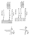
- the XPS results show energy peaks related to the Ag 3d and the Cl 2p electronic orbits as shown in Fig 4.
- AgCl can be expected to behave in a similar manner to other forms of silver halide as the electronic structure of each are very similar. Nevertheless, the exact values can not be deducted using the energy peak values of the other silver halides, but does provide a close enough idea of the expected energy shift range. Furthermore, quantification of the different elements existing at the surface of the silver thin-film, showed that silver and chlorine are the main species (respectively 75% to 80% and 12% to 17%), and only very few contaminants are present (i.e. carbon and oxygen). Thus, only few oxide forms of silver must be created, leaving the shift in the peaks under the influence of the chlorine ions.
- Chlorine was also detected in a chloride form, as the Cl 2p 3/2 peaks are within the same region of binding energy as the alkali chloride, as shown in Fig 5, with an energy shift of about -0.25eV. Even if this chloride shift is compared to a non-metal chloride form, one can still assume that the structure of AgCl and NaCl are close enough to give a very similar electronic distribution of the molecular orbits (M.O.), and hence an analogous shift value.
- M.O. molecular orbits
- the texture and macro-appearance of the plasma electrodes are not similar to the electrochemical electrodes and this is clearly shown by comparison of Fig 2(a) and Fig 2(b).
- the plasma electrodes gave a matt yellowish colour, as described for abnormally electrochlorided electrodes in Crenner et al.
- the present invention provides a method for providing silver modification by chlorine, to produce thin-film silver electrodes with a very controlled surface. Such electrodes can provide quantitative quality of measurement.
Landscapes
- Chemical & Material Sciences (AREA)
- Chemical Kinetics & Catalysis (AREA)
- Engineering & Computer Science (AREA)
- Materials Engineering (AREA)
- Mechanical Engineering (AREA)
- Metallurgy (AREA)
- Organic Chemistry (AREA)
- Life Sciences & Earth Sciences (AREA)
- Health & Medical Sciences (AREA)
- Physics & Mathematics (AREA)
- Pathology (AREA)
- Electrochemistry (AREA)
- Molecular Biology (AREA)
- Analytical Chemistry (AREA)
- Biochemistry (AREA)
- General Health & Medical Sciences (AREA)
- General Physics & Mathematics (AREA)
- Immunology (AREA)
- Inorganic Chemistry (AREA)
- Electrodes For Compound Or Non-Metal Manufacture (AREA)
- Analysing Materials By The Use Of Radiation (AREA)
- Investigating Or Analyzing Materials By The Use Of Electric Means (AREA)
- Physical Vapour Deposition (AREA)
- Manufacture Of Metal Powder And Suspensions Thereof (AREA)
- Chemically Coating (AREA)
- Manufacture And Refinement Of Metals (AREA)
- Physical Or Chemical Processes And Apparatus (AREA)
Claims (15)
- Ein Verfahren zum Reduzieren der Impedanz einer Oberfläche einer Silberelektrode, wobei die Oberfläche mit einem Chlorplasma behandelt wird.
- Verfahren gemäß Anspruch 1, wobei die Silberelektrode in der Form einer Dünnschicht aus Silber vorliegt.
- Verfahren gemäß Anspruch 2, wobei die Elektrode durch eine Verdampfung von Silber auf eine Glasscheibe gefertigt wird.
- Verfahren gemäß Anspruch 3, wobei die Glasscheibe vor der Zugabe von Silber mit einer dünnen metallischen Unterschicht beschichtet wird.
- Verfahren gemäß Anspruch 4, wobei die Unterschicht ein Chrom oder Nichrom ist.
- Verfahren gemäß Anspruch 5, wobei die Unterschicht unter Verwendung eines Sputtersystems auf die Glasscheibe aufgetragen ist.
- Verfahren gemäß einem der vorhergehenden Ansprüche, wobei das Verfahren in einer Plasmakammer ausgeführt wird.
- Verfahren gemäß Anspruch 7, wobei die Plasmakammer eine Reaktives Ionenätzen Radiofrequenz-Plasmakammer ist.
- Verfahren gemäß Anspruch 7 oder Anspruch 8, wobei die Plasmakammer vor der Modifizierung der Silberelektrode oder Metalloberfläche abgepumpt wird.
- Verfahren gemäß Anspruch 9, wobei sich der Betriebsdruck in der Plasmakammer innerhalb des Bereichs von 1 bis 100 mTorr befindet.
- Verfahren gemäß einem der vorhergehenden Ansprüche, wobei sich der Betriebsdruck im Bereich von 5 bis 500 Watt (pro cm2) befindet.
- Verfahren gemäß einem der vorhergehenden Ansprüche, wobei sich das Betriebsflussdichteverfahren im Bereich von 1 bis 50 sccms Gas befindet.
- Verfahren gemäß Anspruch 12, wobei das Gas Chlor ist.
- Verfahren gemäß einem der vorhergehenden Ansprüche, wobei sich die Betriebszeit im Bereich von 1 ms bis 5 Sekunden Plasmazeit befindet.
- Eine Silberelektrode mit einer Oberflächenschicht aus Silberchlorid, die durch Plasmamodifizierung bereitgestellt wird.
Applications Claiming Priority (3)
| Application Number | Priority Date | Filing Date | Title |
|---|---|---|---|
| GB0026276 | 2000-10-27 | ||
| GBGB0026276.6A GB0026276D0 (en) | 2000-10-27 | 2000-10-27 | Method for chlorine plasma modification of silver electrodes |
| PCT/GB2001/004757 WO2002035221A1 (en) | 2000-10-27 | 2001-10-29 | Method for chlorine plasma modification of silver electrodes |
Publications (2)
| Publication Number | Publication Date |
|---|---|
| EP1330642A1 EP1330642A1 (de) | 2003-07-30 |
| EP1330642B1 true EP1330642B1 (de) | 2007-11-14 |
Family
ID=9902048
Family Applications (1)
| Application Number | Title | Priority Date | Filing Date |
|---|---|---|---|
| EP01980648A Expired - Lifetime EP1330642B1 (de) | 2000-10-27 | 2001-10-29 | Verfahren zur modifizierung von silber-elektroden mittels eines chlorplasmas |
Country Status (9)
| Country | Link |
|---|---|
| US (1) | US20040069654A1 (de) |
| EP (1) | EP1330642B1 (de) |
| JP (1) | JP4368108B2 (de) |
| KR (1) | KR20030055291A (de) |
| AT (1) | ATE378586T1 (de) |
| AU (1) | AU2002212443A1 (de) |
| DE (1) | DE60131440T2 (de) |
| GB (1) | GB0026276D0 (de) |
| WO (1) | WO2002035221A1 (de) |
Cited By (1)
| Publication number | Priority date | Publication date | Assignee | Title |
|---|---|---|---|---|
| US12529134B1 (en) | 2023-01-04 | 2026-01-20 | Rhythmlink International, Llc | Methods of making silver/silver chloride electrodes by vapor deposition techniques |
Families Citing this family (15)
| Publication number | Priority date | Publication date | Assignee | Title |
|---|---|---|---|---|
| WO2004073763A1 (en) * | 2003-02-20 | 2004-09-02 | Drm International | Antimicrobial and electrically conducting materials |
| EP1638699A4 (de) * | 2003-05-02 | 2008-04-02 | Noble Fiber Technologies Llc | Verbesserte metallionenabgaberate für antimikrobielle anwendungen |
| JP2007284276A (ja) * | 2006-04-14 | 2007-11-01 | Nippon Sheet Glass Co Ltd | 導電性セラミックス焼結体付き窓ガラス及びその製造方法 |
| SK51082006A3 (sk) * | 2006-12-05 | 2008-07-07 | Fakulta Matematiky, Fyziky A Informatiky Univerzitfakulta Matematiky, Fyziky A Informatiky Univerzity Komensk�Hoy Komensk�Ho | Zariadenie a spôsob úpravy povrchov kovov a metaloZariadenie a spôsob úpravy povrchov kovov a metaloidov, oxidov kovov a oxidov metaloidov a nitridovidov, oxidov kovov a oxidov metaloidov a nitridovkovov a nitridov metaloidovkovov a nitridov metaloidov |
| US20100196203A1 (en) | 2007-02-20 | 2010-08-05 | Gurdial Singh Sanghera | Formation of Lipid Bilayers |
| GB0724736D0 (en) | 2007-12-19 | 2008-01-30 | Oxford Nanolabs Ltd | Formation of layers of amphiphilic molecules |
| US8753561B2 (en) * | 2008-06-20 | 2014-06-17 | Baxter International Inc. | Methods for processing substrates comprising metallic nanoparticles |
| GB201202519D0 (en) | 2012-02-13 | 2012-03-28 | Oxford Nanopore Tech Ltd | Apparatus for supporting an array of layers of amphiphilic molecules and method of forming an array of layers of amphiphilic molecules |
| GB201313121D0 (en) | 2013-07-23 | 2013-09-04 | Oxford Nanopore Tech Ltd | Array of volumes of polar medium |
| GB201611770D0 (en) | 2016-07-06 | 2016-08-17 | Oxford Nanopore Tech | Microfluidic device |
| GB2574048B (en) | 2018-05-24 | 2021-06-16 | Oxford Nanopore Tech Ltd | Nanopore sensor component with electrostatic discharge protection |
| JP7492200B2 (ja) | 2019-03-12 | 2024-05-29 | オックスフォード ナノポール テクノロジーズ ピーエルシー | ナノ細孔センシングデバイスと操作方法およびその成形方法 |
| JP7411672B2 (ja) | 2019-10-11 | 2024-01-11 | タツタ電線株式会社 | 生体用電極 |
| EP4675256A3 (de) | 2020-07-17 | 2026-01-28 | Oxford Nanopore Technologies PLC | Nanoporenmessvorrichtung |
| US12426820B2 (en) | 2020-11-17 | 2025-09-30 | Tatsuta Electric Wire & Cable Co., Ltd. | Biological electrode |
Family Cites Families (6)
| Publication number | Priority date | Publication date | Assignee | Title |
|---|---|---|---|---|
| US5756222A (en) * | 1994-08-15 | 1998-05-26 | Applied Materials, Inc. | Corrosion-resistant aluminum article for semiconductor processing equipment |
| US5874174A (en) * | 1995-08-09 | 1999-02-23 | Matsushita Electric Industrial Co., Ltd. | Conductor film and its forming method |
| US6033582A (en) * | 1996-01-22 | 2000-03-07 | Etex Corporation | Surface modification of medical implants |
| ES2220066T3 (es) * | 1998-06-01 | 2004-12-01 | Roche Diagnostics Corporation | Metodo y dispositivo para inmunoensayo electroquimico de analitos multiples. |
| EP1026500A1 (de) * | 1999-02-01 | 2000-08-09 | Fuji Photo Film Co., Ltd. | Silber/Silberhalogenid-Elektrode und Element mit Ionenselektiver Elektrode |
| AU1455201A (en) * | 1999-11-02 | 2001-05-14 | Advanced Sensor Technologies, Inc. | Batch fabrication of electrodes |
-
2000
- 2000-10-27 GB GBGB0026276.6A patent/GB0026276D0/en not_active Ceased
-
2001
- 2001-10-29 DE DE60131440T patent/DE60131440T2/de not_active Expired - Lifetime
- 2001-10-29 KR KR10-2003-7005841A patent/KR20030055291A/ko not_active Withdrawn
- 2001-10-29 EP EP01980648A patent/EP1330642B1/de not_active Expired - Lifetime
- 2001-10-29 AU AU2002212443A patent/AU2002212443A1/en not_active Abandoned
- 2001-10-29 WO PCT/GB2001/004757 patent/WO2002035221A1/en not_active Ceased
- 2001-10-29 JP JP2002538155A patent/JP4368108B2/ja not_active Expired - Fee Related
- 2001-10-29 US US10/415,194 patent/US20040069654A1/en not_active Abandoned
- 2001-10-29 AT AT01980648T patent/ATE378586T1/de not_active IP Right Cessation
Cited By (1)
| Publication number | Priority date | Publication date | Assignee | Title |
|---|---|---|---|---|
| US12529134B1 (en) | 2023-01-04 | 2026-01-20 | Rhythmlink International, Llc | Methods of making silver/silver chloride electrodes by vapor deposition techniques |
Also Published As
| Publication number | Publication date |
|---|---|
| ATE378586T1 (de) | 2007-11-15 |
| EP1330642A1 (de) | 2003-07-30 |
| US20040069654A1 (en) | 2004-04-15 |
| WO2002035221A1 (en) | 2002-05-02 |
| DE60131440D1 (de) | 2007-12-27 |
| WO2002035221A9 (en) | 2003-05-08 |
| DE60131440T2 (de) | 2008-09-11 |
| JP2004512527A (ja) | 2004-04-22 |
| GB0026276D0 (en) | 2000-12-13 |
| JP4368108B2 (ja) | 2009-11-18 |
| KR20030055291A (ko) | 2003-07-02 |
| AU2002212443A1 (en) | 2002-05-06 |
Similar Documents
| Publication | Publication Date | Title |
|---|---|---|
| US20040069654A1 (en) | Method for chlorine plasma modification of silver electrodes | |
| US5055169A (en) | Method of making mixed metal oxide coated substrates | |
| Milošev et al. | Passive film on orthopaedic TiAlV alloy formed in physiological solution investigated by X-ray photoelectron spectroscopy | |
| JP3027502B2 (ja) | 耐摩耗性非晶質硬質膜及びその製造方法 | |
| TWI870396B (zh) | 電極及電化學測定系統 | |
| Stauf et al. | Iron and nickel thin film deposition via metallocene decomposition | |
| EP3642605B1 (de) | Physikalisch dampfabgeschiedene elektrode für elektrochemische sensoren | |
| Armstrong et al. | Electrochemical and surface characteristics of tin oxide and indium oxide electrodes | |
| Hatada et al. | Preparation of hydrophobic diamond like carbon films by plasma source ion implantation | |
| Flis et al. | Changes in hydrogen entry rate and in surface of iron during cathodic polarisation in alkaline solutions | |
| Scheffel et al. | Reactive high-rate deposition of titanium oxide coatings using electron beam evaporation, spotless arc and dual crucible | |
| JPH07103461B2 (ja) | 黒色皮膜の形成方法及びその皮膜 | |
| Palomäki et al. | Characterization and electrochemical properties of oxygenated amorphous carbon (aC) films | |
| Nitta et al. | Diamond-like carbon thin film with controlled zeta potential for medical material application | |
| US7763150B2 (en) | Method and device for magnetron sputtering | |
| US11561220B2 (en) | Electrode for electrochemical sensors | |
| De Benedetto et al. | Analysis by X-ray photoelectron spectroscopy of ruthenium stabilised polynuclear hexacyanometallate film electrodes | |
| Vershinin et al. | Corrosion resistance of the vacuum arc deposited Ti, TiN and TiO2 coatings on large area glass substrates | |
| Chen et al. | Field emission properties and surface structure of nickel containing amorphous carbon | |
| Juzeliūnas et al. | Study of initial stages of Al–Mg alloy corrosion in water, chloride and Cu (II) environment by a scanning Kelvin probe | |
| RU2100476C1 (ru) | Способ получения защитно-декоративных покрытий | |
| KR20260036035A (ko) | 전극 및 전기 화학 측정 시스템 | |
| Silvain et al. | Chemical and structural analysis of TiAl thin films sputter deposited on carbon substrates | |
| KR100444028B1 (ko) | 은-염화은 전극 제조방법 | |
| Tamašiūnaitė et al. | EQCM study of electrochemical modification of Bi2S3 films in the Zn2+-containing electrolyte |
Legal Events
| Date | Code | Title | Description |
|---|---|---|---|
| PUAI | Public reference made under article 153(3) epc to a published international application that has entered the european phase |
Free format text: ORIGINAL CODE: 0009012 |
|
| 17P | Request for examination filed |
Effective date: 20030503 |
|
| AK | Designated contracting states |
Designated state(s): AT BE CH CY DE DK ES FI FR GB GR IE IT LI LU MC NL PT SE TR |
|
| AX | Request for extension of the european patent |
Extension state: AL LT LV MK RO SI |
|
| 17Q | First examination report despatched |
Effective date: 20050609 |
|
| 17Q | First examination report despatched |
Effective date: 20050609 |
|
| GRAP | Despatch of communication of intention to grant a patent |
Free format text: ORIGINAL CODE: EPIDOSNIGR1 |
|
| GRAS | Grant fee paid |
Free format text: ORIGINAL CODE: EPIDOSNIGR3 |
|
| GRAA | (expected) grant |
Free format text: ORIGINAL CODE: 0009210 |
|
| AK | Designated contracting states |
Kind code of ref document: B1 Designated state(s): AT BE CH CY DE DK ES FI FR GB GR IE IT LI LU MC NL PT SE TR |
|
| REG | Reference to a national code |
Ref country code: GB Ref legal event code: FG4D |
|
| REG | Reference to a national code |
Ref country code: CH Ref legal event code: EP |
|
| REG | Reference to a national code |
Ref country code: IE Ref legal event code: FG4D |
|
| REF | Corresponds to: |
Ref document number: 60131440 Country of ref document: DE Date of ref document: 20071227 Kind code of ref document: P |
|
| PG25 | Lapsed in a contracting state [announced via postgrant information from national office to epo] |
Ref country code: CH Free format text: LAPSE BECAUSE OF FAILURE TO SUBMIT A TRANSLATION OF THE DESCRIPTION OR TO PAY THE FEE WITHIN THE PRESCRIBED TIME-LIMIT Effective date: 20071114 Ref country code: SE Free format text: LAPSE BECAUSE OF FAILURE TO SUBMIT A TRANSLATION OF THE DESCRIPTION OR TO PAY THE FEE WITHIN THE PRESCRIBED TIME-LIMIT Effective date: 20080214 Ref country code: ES Free format text: LAPSE BECAUSE OF FAILURE TO SUBMIT A TRANSLATION OF THE DESCRIPTION OR TO PAY THE FEE WITHIN THE PRESCRIBED TIME-LIMIT Effective date: 20080225 Ref country code: LI Free format text: LAPSE BECAUSE OF FAILURE TO SUBMIT A TRANSLATION OF THE DESCRIPTION OR TO PAY THE FEE WITHIN THE PRESCRIBED TIME-LIMIT Effective date: 20071114 Ref country code: NL Free format text: LAPSE BECAUSE OF FAILURE TO SUBMIT A TRANSLATION OF THE DESCRIPTION OR TO PAY THE FEE WITHIN THE PRESCRIBED TIME-LIMIT Effective date: 20071114 |
|
| NLV1 | Nl: lapsed or annulled due to failure to fulfill the requirements of art. 29p and 29m of the patents act | ||
| PG25 | Lapsed in a contracting state [announced via postgrant information from national office to epo] |
Ref country code: FI Free format text: LAPSE BECAUSE OF FAILURE TO SUBMIT A TRANSLATION OF THE DESCRIPTION OR TO PAY THE FEE WITHIN THE PRESCRIBED TIME-LIMIT Effective date: 20071114 |
|
| REG | Reference to a national code |
Ref country code: CH Ref legal event code: PL |
|
| PG25 | Lapsed in a contracting state [announced via postgrant information from national office to epo] |
Ref country code: AT Free format text: LAPSE BECAUSE OF FAILURE TO SUBMIT A TRANSLATION OF THE DESCRIPTION OR TO PAY THE FEE WITHIN THE PRESCRIBED TIME-LIMIT Effective date: 20071114 |
|
| ET | Fr: translation filed | ||
| PG25 | Lapsed in a contracting state [announced via postgrant information from national office to epo] |
Ref country code: DK Free format text: LAPSE BECAUSE OF FAILURE TO SUBMIT A TRANSLATION OF THE DESCRIPTION OR TO PAY THE FEE WITHIN THE PRESCRIBED TIME-LIMIT Effective date: 20071114 |
|
| PG25 | Lapsed in a contracting state [announced via postgrant information from national office to epo] |
Ref country code: BE Free format text: LAPSE BECAUSE OF FAILURE TO SUBMIT A TRANSLATION OF THE DESCRIPTION OR TO PAY THE FEE WITHIN THE PRESCRIBED TIME-LIMIT Effective date: 20071114 |
|
| PLBE | No opposition filed within time limit |
Free format text: ORIGINAL CODE: 0009261 |
|
| STAA | Information on the status of an ep patent application or granted ep patent |
Free format text: STATUS: NO OPPOSITION FILED WITHIN TIME LIMIT |
|
| PG25 | Lapsed in a contracting state [announced via postgrant information from national office to epo] |
Ref country code: PT Free format text: LAPSE BECAUSE OF FAILURE TO SUBMIT A TRANSLATION OF THE DESCRIPTION OR TO PAY THE FEE WITHIN THE PRESCRIBED TIME-LIMIT Effective date: 20080414 |
|
| 26N | No opposition filed |
Effective date: 20080815 |
|
| PG25 | Lapsed in a contracting state [announced via postgrant information from national office to epo] |
Ref country code: GR Free format text: LAPSE BECAUSE OF FAILURE TO SUBMIT A TRANSLATION OF THE DESCRIPTION OR TO PAY THE FEE WITHIN THE PRESCRIBED TIME-LIMIT Effective date: 20080215 |
|
| PG25 | Lapsed in a contracting state [announced via postgrant information from national office to epo] |
Ref country code: MC Free format text: LAPSE BECAUSE OF NON-PAYMENT OF DUE FEES Effective date: 20081031 |
|
| PG25 | Lapsed in a contracting state [announced via postgrant information from national office to epo] |
Ref country code: CY Free format text: LAPSE BECAUSE OF FAILURE TO SUBMIT A TRANSLATION OF THE DESCRIPTION OR TO PAY THE FEE WITHIN THE PRESCRIBED TIME-LIMIT Effective date: 20071114 |
|
| PG25 | Lapsed in a contracting state [announced via postgrant information from national office to epo] |
Ref country code: IE Free format text: LAPSE BECAUSE OF NON-PAYMENT OF DUE FEES Effective date: 20081029 |
|
| PG25 | Lapsed in a contracting state [announced via postgrant information from national office to epo] |
Ref country code: LU Free format text: LAPSE BECAUSE OF NON-PAYMENT OF DUE FEES Effective date: 20081029 |
|
| PG25 | Lapsed in a contracting state [announced via postgrant information from national office to epo] |
Ref country code: TR Free format text: LAPSE BECAUSE OF FAILURE TO SUBMIT A TRANSLATION OF THE DESCRIPTION OR TO PAY THE FEE WITHIN THE PRESCRIBED TIME-LIMIT Effective date: 20071114 |
|
| PG25 | Lapsed in a contracting state [announced via postgrant information from national office to epo] |
Ref country code: IT Free format text: LAPSE BECAUSE OF NON-PAYMENT OF DUE FEES Effective date: 20091029 |
|
| PGRI | Patent reinstated in contracting state [announced from national office to epo] |
Ref country code: IT Effective date: 20110616 |
|
| REG | Reference to a national code |
Ref country code: FR Ref legal event code: PLFP Year of fee payment: 15 |
|
| REG | Reference to a national code |
Ref country code: FR Ref legal event code: TP Owner name: INTELESENS LIMITED, IE Effective date: 20151029 |
|
| REG | Reference to a national code |
Ref country code: GB Ref legal event code: 732E Free format text: REGISTERED BETWEEN 20151112 AND 20151118 |
|
| REG | Reference to a national code |
Ref country code: DE Ref legal event code: R081 Ref document number: 60131440 Country of ref document: DE Owner name: INTELESENS LIMITED, GB Free format text: FORMER OWNER: INNOVATION ULSTER LIMITED, COLERAINE, NORTHERN IRELAND, GB Ref country code: DE Ref legal event code: R081 Ref document number: 60131440 Country of ref document: DE Owner name: INTELESENS LIMITED, GB Free format text: FORMER OWNER: UUTECH LTD., COLERAINE, NORTHERN IRELAND, IE Ref country code: DE Ref legal event code: R082 Ref document number: 60131440 Country of ref document: DE Representative=s name: MURGITROYD & COMPANY, DE |
|
| REG | Reference to a national code |
Ref country code: FR Ref legal event code: RM Effective date: 20160609 |
|
| REG | Reference to a national code |
Ref country code: FR Ref legal event code: PLFP Year of fee payment: 16 |
|
| REG | Reference to a national code |
Ref country code: FR Ref legal event code: PLFP Year of fee payment: 17 |
|
| REG | Reference to a national code |
Ref country code: FR Ref legal event code: PLFP Year of fee payment: 17 |
|
| REG | Reference to a national code |
Ref country code: FR Ref legal event code: PLFP Year of fee payment: 18 |
|
| PGFP | Annual fee paid to national office [announced via postgrant information from national office to epo] |
Ref country code: FR Payment date: 20190917 Year of fee payment: 19 |
|
| PGFP | Annual fee paid to national office [announced via postgrant information from national office to epo] |
Ref country code: GB Payment date: 20190916 Year of fee payment: 19 |
|
| PGFP | Annual fee paid to national office [announced via postgrant information from national office to epo] |
Ref country code: DE Payment date: 20190917 Year of fee payment: 19 |
|
| PGFP | Annual fee paid to national office [announced via postgrant information from national office to epo] |
Ref country code: IT Payment date: 20190926 Year of fee payment: 19 |
|
| REG | Reference to a national code |
Ref country code: DE Ref legal event code: R119 Ref document number: 60131440 Country of ref document: DE |
|
| GBPC | Gb: european patent ceased through non-payment of renewal fee |
Effective date: 20201029 |
|
| PG25 | Lapsed in a contracting state [announced via postgrant information from national office to epo] |
Ref country code: DE Free format text: LAPSE BECAUSE OF NON-PAYMENT OF DUE FEES Effective date: 20210501 Ref country code: FR Free format text: LAPSE BECAUSE OF NON-PAYMENT OF DUE FEES Effective date: 20201031 |
|
| PG25 | Lapsed in a contracting state [announced via postgrant information from national office to epo] |
Ref country code: GB Free format text: LAPSE BECAUSE OF NON-PAYMENT OF DUE FEES Effective date: 20201029 |
|
| PG25 | Lapsed in a contracting state [announced via postgrant information from national office to epo] |
Ref country code: IT Free format text: LAPSE BECAUSE OF NON-PAYMENT OF DUE FEES Effective date: 20201031 |