EP1330057A1 - Electric field intensity detecting circuit and limiter amplifier - Google Patents
Electric field intensity detecting circuit and limiter amplifier Download PDFInfo
- Publication number
- EP1330057A1 EP1330057A1 EP01972481A EP01972481A EP1330057A1 EP 1330057 A1 EP1330057 A1 EP 1330057A1 EP 01972481 A EP01972481 A EP 01972481A EP 01972481 A EP01972481 A EP 01972481A EP 1330057 A1 EP1330057 A1 EP 1330057A1
- Authority
- EP
- European Patent Office
- Prior art keywords
- differential
- differential amplifiers
- electric field
- transistors
- field intensity
- Prior art date
- Legal status (The legal status is an assumption and is not a legal conclusion. Google has not performed a legal analysis and makes no representation as to the accuracy of the status listed.)
- Withdrawn
Links
- 230000005684 electric field Effects 0.000 title claims description 24
- 230000003321 amplification Effects 0.000 abstract description 11
- 238000003199 nucleic acid amplification method Methods 0.000 abstract description 11
- 238000001514 detection method Methods 0.000 abstract description 10
- 238000010586 diagram Methods 0.000 description 8
- 239000003990 capacitor Substances 0.000 description 1
- 230000015556 catabolic process Effects 0.000 description 1
- 238000006731 degradation reaction Methods 0.000 description 1
- 238000009499 grossing Methods 0.000 description 1
- 238000000034 method Methods 0.000 description 1
- 229920006395 saturated elastomer Polymers 0.000 description 1
Images


Classifications
-
- G—PHYSICS
- G01—MEASURING; TESTING
- G01R—MEASURING ELECTRIC VARIABLES; MEASURING MAGNETIC VARIABLES
- G01R29/00—Arrangements for measuring or indicating electric quantities not covered by groups G01R19/00 - G01R27/00
- G01R29/08—Measuring electromagnetic field characteristics
-
- H—ELECTRICITY
- H03—ELECTRONIC CIRCUITRY
- H03F—AMPLIFIERS
- H03F3/00—Amplifiers with only discharge tubes or only semiconductor devices as amplifying elements
Definitions
- the present invention relates to an electric field intensity detecting circuit and a limiter amplifier and particularly concerns an electric field intensity detecting circuit improved to obtain an electric field intensity detecting signal with preferred linearity and a limiter amplified used for the circuit.
- electric field intensity detecting circuits are used for electronic equipment such as a radio receiver, a portable phone, a cordless phone, and a television receiving set that receives and processes a high-frequency signal (RF signal).
- the electric field intensity detecting circuits detect electric field intensity of a received high-frequency signal and output a DC signal at a level equivalent to the electric field intensity.
- FIG. 1 is a diagram showing the configuration of a conventional electric field intensity detecting circuit.
- a high-pass filter 1 on the input stage is constituted by a capacitor C and a resistor R.
- n differential amplifiers 2, 3, and 4 make multi-stage connection to the post stage of the high-pass filter 1.
- the n differential amplifiers 2, 3, and 4 making multi-stage connection constitute a limiter amplifier.
- the drains of the transistors Q i1 and Q i2 are connected to a power supply VDD respectively via the resistors R i1 and R i2 .
- An input signal V in passing through the high-pass filter 1 is inputted to the gates of the transistors Q 11 and Q 12 of the differential amplifier 2 on the first stage.
- the above-described transistors Q i and the constant current circuits I form a part of a detector circuit connected to the post stage of the limiter amplifier.
- the detector circuit inputs output signals of the n differential amplifiers 2, 3, and 4, smooth the signals, and outputs the signals, so that a DC electric field intensity detecting signal V DC is obtained.
- FIG. 2 is a diagram showing input/output characteristics of the electric field intensity detecting circuit, that is, the relationship between the input signal V in (voltage value) and the output signal V DC (voltage value).
- the electric field intensity detecting circuit it is desirable to have preferable linearity as much as possible between a logarithm of an input voltage V in and an output voltage V DC .
- the signal V in inputted to the transistors Q 11 and Q 12 of the differential amplifier 2 on the first stage is amplified by a predetermined level and is outputted.
- the transistor Q 11 has a negative phase output and the transistor Q 12 has an in-phase output.
- the amplified and outputted signal is inputted to the bases of the transistors Q 21 and Q 22 of the differential amplifier 3 on the second stage, and the signal is further amplified by the differential amplifier 3 and is outputted.
- a differential amplifier constituting a limiter amplifier is provided only on a single stage, when an amplification factor is large, a signal level is immediately saturated, and when an amplification factor is small, it takes a long time to perform amplification to a desired level. Thus, preferable linearity cannot be obtained with respect to the input/output characteristics.
- a plurality of amplifiers 2, 3, and 4 are connected in multistages to constitute the limiter amplifier.
- the present invention is devised to solve such a problem and has as its object the provision of referable DC detection efficiency while obtaining a large gain of a limiter amplifier having differential amplifiers connected in multistages.
- An electric field intensity detecting circuit comprises a differential amplifier circuit constituted by first differential amplifiers connected in multistages, the first differential amplifiers amplifying an input signal from the preceding stage and outputting the signal to the subsequent stage, and second differential amplifiers arranged in parallel with at least some of the n first differential amplifiers constituting the differential amplifier circuit, and a to-be-detected signal is obtained from the second differential amplifiers.
- the first differential amplifier comprises a differential pair composed of a pair of resistors and a pair of transistors, and a first constant current circuit connected in common to the pair of transistors.
- the second differential amplifier comprises a differential pair composed of a pair of transistors, and a second constant current circuit connected in common to the pair of transistors.
- Another aspect of the present invention is characterized in that the second differential amplifiers are arranged only in parallel with some of the n first differential amplifiers on the post-stage side, the n first differential amplifiers constituting the differential amplifier circuit.
- a limiter amplifier of the present invention comprises a differential amplifier circuit constituted by first differential amplifiers connected in multistages, the first differential amplifiers amplifying an input signal from the preceding stage and outputting the signal to the subsequent stage, and second differential amplifiers arranged in parallel with at least some of the n first differential amplifiers constituting the differential amplifier circuit.
- Another aspect of the present invention is characterized in that the second differential amplifiers are arranged only in parallel with some of the n first differential amplifiers on the post-stage side, the n first differential amplifiers constituting the differential amplifier circuit.
- differential amplification is increased in gain by applying large current to the first constant current circuit constituting the first differential amplifier, and the signal level for detection can be increased by applying small current to the second constant current circuit constituting the second differential amplifier. Hence, preferable detection efficiency can be obtained while a large gain is provided for differential amplification.
- the second differential amplifiers are arranged only in parallel with some of the first differential amplifiers on a post-stage side that require particularly a large gain for differential amplification.
- it is possible to minimize an increase in the number of elements. With this configuration, while suppressing expansion of a circuit area increased with the number of elements, preferable detection efficiency can be obtained with a large gain for differential amplification.
- the electric field intensity detecting circuit of the present embodiment comprises on ith stage a differential amplifier 11 which is constituted by a differential pair of two resistors R i1 and R i2 and two transistors Q i1 and Q i2 and a constant current circuit I i1 .
- the sources of the two transistors Q i1 and Q i2 , which constitute the differential pair, are connected in common, and the constant current circuit I i1 is connected to the common source.
- the drains of the transistors Q i1 and Q i2 are each connected to a power supply VDD via the resistors R i1 and R i2 .
- an output signal from a first differential amplifier on the preceding stage is inputted to the gates of the transistors O i1 and Q i2 .
- an input signal V in passing through a high-pass filter 1 of FIG. 1 is inputted to the gates of the transistors Q i1 and Q i2 of the differential amplifier on the first stage.
- the first differential amplifier 11 is similar to differential amplifiers 2, 3, and 4 shown in FIG. 1.
- a second differential amplifier 12 is further provided in parallel.
- the second differential amplifier 12 is constituted by a differential pair of two transistors Q i3 and Q i4 and a constant current circuit I i2 . Namely, the sources of the two transistors Q i3 and Q i4 constituting the differential pair are connected in common, and the constant current circuit I i2 is connected to the common source.
- the common sources of the transistors Q i1 and Q i2 constituting the first differential amplifier 11 instead of the common sources of the transistors Q i3 and Q i4 constituting the second differential amplifier 12, which is additionally provided in the present embodiment, are connected to the gate of a transistor Q i constituting a detector circuit.
- the constant current circuits I i1 and I i2 constituting the two differential amplifiers 11 and 12 a relatively high current is applied to the constant current circuit I i1 as in the conventional art.
- differential amplification can obtain a large gain.
- a relatively low current is applied to the constant current circuit I i2 of the second differential amplifier 12.
- the level of a signal inputted to the gate of the transistor Q i is not lower than the original level, and preferable DC detection efficiency can be maintained.
- the number of connected stages is, for example, 6 to 8.
- the second differential amplifiers 12 are provided thus on all the stages making multi-stage connection, the second differential amplifiers 12 may be provided at least only on some of the stages.
- the number of elements is larger due to the second differential amplifiers 12 as compared with the conventional electric field intensity detecting circuit.
- the second differential amplifiers 12 are added only on necessary stages, so that an increase in the number of elements can be suppressed.
- the post-stage side is larger in gain of differential amplitude than the first stage side of the differential amplifiers 11 making multi-stage connection.
- the following configuration is applicable: on several stages from the first stage, only the first differential amplifiers 11 are provided and the second differential amplifiers 12 are not provided, and only on several stages from the last stage (e.g., two stages from the last), the second differential amplifiers 12 are provided.
- the present invention is useful for obtaining preferable DC detection efficiency while achieving a large gain for a limiter amplifier where differential amplifiers are connected in multistages.
Landscapes
- Physics & Mathematics (AREA)
- Electromagnetism (AREA)
- General Physics & Mathematics (AREA)
- Engineering & Computer Science (AREA)
- Power Engineering (AREA)
- Amplifiers (AREA)
- Tone Control, Compression And Expansion, Limiting Amplitude (AREA)
Abstract
A second differential amplifier (12) is additionally
disposed in parallel with at least a part of first differential
amplifiers (11) in respect to a differential amplifying circuit
comprising a multi-stage connection of the first differential
amplifiers (11) so that a to-be-detected signal may be obtained
from the second differential amplifier (12) to a transistor
(Qi). Thus, a large current is made to flow through a constant
current circuit (Ii1) which constitutes the first differential
amplifier (11) to increase a differential amplification gain.
A small current is made to flow through a constant current
circuit (Ii12) which constitutes the second differential
amplifier (12), thereby increasing the signal level for
detection.
Description
- The present invention relates to an electric field intensity detecting circuit and a limiter amplifier and particularly concerns an electric field intensity detecting circuit improved to obtain an electric field intensity detecting signal with preferred linearity and a limiter amplified used for the circuit.
- In general, electric field intensity detecting circuits are used for electronic equipment such as a radio receiver, a portable phone, a cordless phone, and a television receiving set that receives and processes a high-frequency signal (RF signal). The electric field intensity detecting circuits detect electric field intensity of a received high-frequency signal and output a DC signal at a level equivalent to the electric field intensity.
- FIG. 1 is a diagram showing the configuration of a conventional electric field intensity detecting circuit. In FIG. 1, a high-
pass filter 1 on the input stage is constituted by a capacitor C and a resistor R. ndifferential amplifiers 2, 3, and 4 make multi-stage connection to the post stage of the high-pass filter 1. The ndifferential amplifiers 2, 3, and 4 making multi-stage connection constitute a limiter amplifier. - The
differential amplifiers 2, 3, and 4 are each constituted by a differential pair of two resistors Ri1 and Ri2 (i = 1 to n) and two transistors Qi1 and Qi2 (i = 1 to n) and a constant current circuit Ii (i = 1 to n). Namely, the sources of the two transistors Qi1 and Qi2 constituting each differential pair are connected in common, and the constant current circuits Ii (i = 1 to n) are respectively connected to the common sources. Further, the common sources of the transistors Qi1 and Qi2 are each connected to a constant current circuit I via transistors Qi (i = 1 to n). - Moreover, the drains of the transistors Qi1 and Qi2 are connected to a power supply VDD respectively via the resistors Ri1 and Ri2. Also, except for the
differential amplifier 2 on the first stage, an output signal VOUTi (i = 1 to n - 1) from the differential amplifier on the preceding stage is inputted to the gates of the transistors Qi1 and Qi2. An input signal Vin passing through the high-pass filter 1 is inputted to the gates of the transistors Q11 and Q12 of thedifferential amplifier 2 on the first stage. - The above-described transistors Qi and the constant current circuits I form a part of a detector circuit connected to the post stage of the limiter amplifier. The detector circuit inputs output signals of the n
differential amplifiers 2, 3, and 4, smooth the signals, and outputs the signals, so that a DC electric field intensity detecting signal VDC is obtained. - FIG. 2 is a diagram showing input/output characteristics of the electric field intensity detecting circuit, that is, the relationship between the input signal Vin (voltage value) and the output signal VDC (voltage value). In the electric field intensity detecting circuit, it is desirable to have preferable linearity as much as possible between a logarithm of an input voltage Vin and an output voltage VDC. For example, in the case of a radio receiver, it is necessary to have linearity over a wide range of about [dBµ] (1 µV) to 80 [dBµ] (10 mV). For this reason, a plurality of differential amplifiers constituting a limiter amplifier are provided and are connected in multistages, and the
differential amplifiers 2, 3, and 4 on the respective stages are adjusted in gain according to a magnitude of current applied to the constant current circuits Ii (i = 1 to n). - Namely, in the limiter amplifier configured thus, the signal Vin inputted to the transistors Q11 and Q12 of the
differential amplifier 2 on the first stage is amplified by a predetermined level and is outputted. In this circuit, the transistor Q11 has a negative phase output and the transistor Q12 has an in-phase output. The amplified and outputted signal is inputted to the bases of the transistors Q21 and Q22 of the differential amplifier 3 on the second stage, and the signal is further amplified by the differential amplifier 3 and is outputted. - Thereafter, the signal is similarly amplified increasingly by the
differential amplifiers 2, 3, and 4 on the respective stages. Hence, the signal Vin inputted to thedifferential amplifier 2 on the first stage increases in amplitude as the signal proceeds to latter stages. However, since signal output levels on the respective stages do not exceed the power supply voltage VDD, saturation is made without amplification exceeding a certain level of the signal inputted to each of the stages. - Since a signal inputted to the differential amplifier 4 on the nth stage has the highest level as compared with the other stages, saturation is made most quickly at a low input level. Meanwhile, since a signal input level Vin on the first stage is the lowest as compared with the other stages, saturation cannot be made without inputting up to a high-input level. By smoothing output voltages of the
differential amplifiers 2, 3, and 4 on the respective stages that have such characteristics, preferable linearity is obtained as much as possible as shown in FIG. 2. - In the case where a differential amplifier constituting a limiter amplifier is provided only on a single stage, when an amplification factor is large, a signal level is immediately saturated, and when an amplification factor is small, it takes a long time to perform amplification to a desired level. Thus, preferable linearity cannot be obtained with respect to the input/output characteristics. Hence, as described above, a plurality of
amplifiers 2, 3, and 4 are connected in multistages to constitute the limiter amplifier. - In this case, in order to obtain a predetermined gain in each of the
differential amplifiers 2, 3, and 4 on the respective stages, current needs to be applied to the constant current circuits Ii (i = 1 to n) on the respective stages so as to match the gain. At this point, since the differential amplifier 4 on the nth stage has the largest gain, the corresponding constant current circuit In has to be fed with larger current as compared with the other stages. - However, when current applied to the constant current circuits Ii (i = 1 to n) is increased to obtain a large gain, the levels of signals (voltage levels of nodes a1 to an shown in FIG. 1) inputted to the transistors Qi (i = 1 ton) constituting the detector circuit become lower than the original level, resulting in degradation in DC detection efficiency. This will be described below in accordance with FIG. 3.
- FIG. 3 is a diagram showing waveforms of signals (signals indicated on the nodes a1 to an) inputted to the gates of the transistors Qi (i = 1 to n). Since the constant current circuit Ii increases in current value with latter stages (the node an side) of the limiter amplifier, as shown in FIG. 3, a signal level on the post-stage side peaks out and becomes lower than the original level. Hence, DC detection efficiency is reduced and a signal remaining AC passes particularly on the post-stage side. Thus, the above-described linearity cannot be obtained.
- The present invention is devised to solve such a problem and has as its object the provision of referable DC detection efficiency while obtaining a large gain of a limiter amplifier having differential amplifiers connected in multistages.
- An electric field intensity detecting circuit comprises a differential amplifier circuit constituted by first differential amplifiers connected in multistages, the first differential amplifiers amplifying an input signal from the preceding stage and outputting the signal to the subsequent stage, and second differential amplifiers arranged in parallel with at least some of the n first differential amplifiers constituting the differential amplifier circuit, and a to-be-detected signal is obtained from the second differential amplifiers.
- Another aspect of the present invention is characterized in that the first differential amplifier comprises a differential pair composed of a pair of resistors and a pair of transistors, and a first constant current circuit connected in common to the pair of transistors.
- Another aspect of the present invention is characterized in that the second differential amplifier comprises a differential pair composed of a pair of transistors, and a second constant current circuit connected in common to the pair of transistors.
- Another aspect of the present invention is characterized in that the second differential amplifiers are arranged only in parallel with some of the n first differential amplifiers on the post-stage side, the n first differential amplifiers constituting the differential amplifier circuit.
- Further, a limiter amplifier of the present invention comprises a differential amplifier circuit constituted by first differential amplifiers connected in multistages, the first differential amplifiers amplifying an input signal from the preceding stage and outputting the signal to the subsequent stage, and second differential amplifiers arranged in parallel with at least some of the n first differential amplifiers constituting the differential amplifier circuit.
- Another aspect of the present invention is characterized in that the second differential amplifiers are arranged only in parallel with some of the n first differential amplifiers on the post-stage side, the n first differential amplifiers constituting the differential amplifier circuit.
- Since the present invention is achieved by the above technical means, differential amplification is increased in gain by applying large current to the first constant current circuit constituting the first differential amplifier, and the signal level for detection can be increased by applying small current to the second constant current circuit constituting the second differential amplifier. Hence, preferable detection efficiency can be obtained while a large gain is provided for differential amplification.
- According to another aspect of the present invention, the second differential amplifiers are arranged only in parallel with some of the first differential amplifiers on a post-stage side that require particularly a large gain for differential amplification. Thus, it is possible to minimize an increase in the number of elements. With this configuration, while suppressing expansion of a circuit area increased with the number of elements, preferable detection efficiency can be obtained with a large gain for differential amplification.
-
- FIG. 1 is a diagram showing the configuration of a conventional electric field intensity detecting circuit;
- FIG. 2 is a diagram showing input/output characteristics of the electric field intensity detecting circuit;
- FIG. 3 is a diagram showing waveforms of signals inputted to the gates of transistors Qi; and
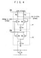
- FIG. 4 is a diagram showing a part of the configuration of an electric field intensity detecting circuit according to the present embodiment.
-
- The following will discuss an embodiment of the present invention in accordance with the accompanied drawing.
- FIG. 4 is a diagram showing a part of the configuration of an electric field intensity detecting circuit according to the present embodiment. Although FIG. 4 shows the configuration of ith stage, the similar configuration is connected in multistages until i = 1 to n.
- As shown in FIG. 4, the electric field intensity detecting circuit of the present embodiment comprises on ith stage a
differential amplifier 11 which is constituted by a differential pair of two resistors Ri1 and Ri2 and two transistors Qi1 and Qi2 and a constant current circuit Ii1. The sources of the two transistors Qi1 and Qi2, which constitute the differential pair, are connected in common, and the constant current circuit Ii1 is connected to the common source. - Further, the drains of the transistors Qi1 and Qi2 are each connected to a power supply VDD via the resistors Ri1 and Ri2. Moreover, an output signal from a first differential amplifier on the preceding stage (not shown) is inputted to the gates of the transistors Oi1 and Qi2. Besides, in the case of i = 1 (first stage), an input signal Vin passing through a high-
pass filter 1 of FIG. 1 is inputted to the gates of the transistors Qi1 and Qi2 of the differential amplifier on the first stage. - The first
differential amplifier 11 is similar todifferential amplifiers 2, 3, and 4 shown in FIG. 1. In the present embodiment, in addition to the firstdifferential amplifier 11, a seconddifferential amplifier 12 is further provided in parallel. The seconddifferential amplifier 12 is constituted by a differential pair of two transistors Qi3 and Qi4 and a constant current circuit Ii2. Namely, the sources of the two transistors Qi3 and Qi4 constituting the differential pair are connected in common, and the constant current circuit Ii2 is connected to the common source. - Additionally, the drains of the transistors Qi3 and Qi4 are each connected to the power supply VDD. Further, an output signal from the first differential amplifier on the preceding stage (not shown) is inputted to the gates of the transistors Qi3 and Qi4. Besides, in the case of i = 1 (first stage), the input signal Vin passing through the high-
pass filter 1 shown in FIG. 1 is inputted to the gates of transistors Q13 and Q14 of the differential amplifier on the first stage. - In the electric field intensity detecting circuit of the present embodiment, instead of the common sources of the transistors Qi1 and Qi2 constituting the first
differential amplifier 11, the common sources of the transistors Qi3 and Qi4 constituting the seconddifferential amplifier 12, which is additionally provided in the present embodiment, are connected to the gate of a transistor Qi constituting a detector circuit. - Further, of the constant current circuits Ii1 and Ii2 constituting the two
differential amplifiers differential amplifier 12. Thus, the level of a signal inputted to the gate of the transistor Qi is not lower than the original level, and preferable DC detection efficiency can be maintained. - As described above, the limiter amplifier of the present embodiment is constituted by connecting the configuration of FIG. 4 in multistages until i = 1 to n. The number of connected stages is, for example, 6 to 8. In the present embodiment, although the second
differential amplifiers 12 are provided thus on all the stages making multi-stage connection, the seconddifferential amplifiers 12 may be provided at least only on some of the stages. - Namely, in the present embodiment, the number of elements is larger due to the second
differential amplifiers 12 as compared with the conventional electric field intensity detecting circuit. Hence, when all the stages comprise the seconddifferential amplifiers 12, the number of elements is increased accordingly and results in a larger circuit area. Hence, the seconddifferential amplifiers 12 are added only on necessary stages, so that an increase in the number of elements can be suppressed. - For example, the post-stage side is larger in gain of differential amplitude than the first stage side of the
differential amplifiers 11 making multi-stage connection. Thus, the following configuration is applicable: on several stages from the first stage, only the firstdifferential amplifiers 11 are provided and the seconddifferential amplifiers 12 are not provided, and only on several stages from the last stage (e.g., two stages from the last), the seconddifferential amplifiers 12 are provided. With this configuration, without a large increase the number of elements, preferable DC detection efficiency can be obtained while achieving a large gain for differential amplification. - Additionally, the above-described embodiment just illustrates an example of a concrete form for implementing the present invention and the technical scope of the present invention should not be interpreted in a limited manner. Namely, the present invention can be implemented in various forms without departing from the spirit or the main characteristics of the invention.
- The present invention is useful for obtaining preferable DC detection efficiency while achieving a large gain for a limiter amplifier where differential amplifiers are connected in multistages.
Claims (6)
- An electric field intensity detecting circuit comprises:a differential amplifier circuit constituted by first differential amplifiers connected in multistages, the first differential amplifiers amplifying an input signal from a preceding stage and outputting the signal to a subsequent stage, andsecond differential amplifiers arranged in parallel with at least some of the n first differential amplifiers constituting the differential amplifier circuit, anda to-be-detected signal is obtained from the second differential amplifiers.
- The electric field intensity detecting circuit according to claim 1, the first differential amplifier comprises:a differential pair composed of a pair of resistors and a pair of transistors, anda first constant current circuit connected in common to the pair of transistors.
- The electric field intensity detecting circuit according to claim 1, the second differential amplifier comprises:a differential pair composed of a pair of transistors, anda second constant current circuit connected in common to the pair of transistors.
- The electric field intensity detecting circuit according to claim 1,the second differential amplifiers are arranged only in parallel with some of the n first differential amplifiers on a post-stage side, the n first differential amplifiers constituting the differential amplifier circuit.
- A limiter amplifier comprises:a differential amplifier circuit constituted by first differential amplifiers connected in multistages, the first differential amplifiers amplifying an input signal from a preceding stage and outputting the signal to a subsequent stage, andsecond differential amplifiers arranged in parallel with at least some of the n first differential amplifiers constituting the differential amplifier circuit.
- The limiter amplifier according to claim 5,the second differential amplifiers are arranged only in parallel with some of the n first differential amplifiers on a post-stage side, the n first differential amplifiers constituting the differential amplifier circuit.
Applications Claiming Priority (3)
| Application Number | Priority Date | Filing Date | Title |
|---|---|---|---|
| JP2000308255 | 2000-10-06 | ||
| JP2000308255A JP2002118432A (en) | 2000-10-06 | 2000-10-06 | Field intensity detection circuit and limiter amplifier |
| PCT/JP2001/008336 WO2002033860A1 (en) | 2000-10-06 | 2001-09-26 | Electric field intensity detecting circuit and limiter amplifier |
Publications (1)
| Publication Number | Publication Date |
|---|---|
| EP1330057A1 true EP1330057A1 (en) | 2003-07-23 |
Family
ID=18788599
Family Applications (1)
| Application Number | Title | Priority Date | Filing Date |
|---|---|---|---|
| EP01972481A Withdrawn EP1330057A1 (en) | 2000-10-06 | 2001-09-26 | Electric field intensity detecting circuit and limiter amplifier |
Country Status (7)
| Country | Link |
|---|---|
| US (1) | US6774720B2 (en) |
| EP (1) | EP1330057A1 (en) |
| JP (1) | JP2002118432A (en) |
| KR (1) | KR100843756B1 (en) |
| CN (1) | CN1249938C (en) |
| TW (1) | TW519568B (en) |
| WO (1) | WO2002033860A1 (en) |
Families Citing this family (5)
| Publication number | Priority date | Publication date | Assignee | Title |
|---|---|---|---|---|
| JP4070533B2 (en) * | 2002-07-26 | 2008-04-02 | 富士通株式会社 | Semiconductor integrated circuit device |
| US7339390B2 (en) * | 2005-05-31 | 2008-03-04 | International Business Machines Corporation | Systems and methods for controlling of electro-migration |
| US7279975B2 (en) * | 2005-12-22 | 2007-10-09 | Zuoguo Wu | Differential circuit with offset control |
| CN101729032B (en) * | 2008-10-22 | 2014-06-18 | 杭州士兰微电子股份有限公司 | Gain limiter circuit |
| DE102016115596B4 (en) | 2016-08-23 | 2018-07-12 | Ferro-Carbon Ent. Co., Ltd. | Knife sharpening |
Family Cites Families (6)
| Publication number | Priority date | Publication date | Assignee | Title |
|---|---|---|---|---|
| JPS61166207A (en) * | 1985-01-18 | 1986-07-26 | Nec Corp | Intermediate frequency amplifier circuit with electric field strength detecting function |
| US4680553A (en) | 1985-01-18 | 1987-07-14 | Nec Corporation | Intermediate frequency amplifier with signal strength detection circuit |
| JPH0484509A (en) * | 1990-07-26 | 1992-03-17 | Sharp Corp | Limiter amplifier |
| US5489868A (en) * | 1994-10-04 | 1996-02-06 | Analog Devices, Inc. | Detector cell for logarithmic amplifiers |
| JPH08125559A (en) * | 1994-10-26 | 1996-05-17 | Matsushita Electric Ind Co Ltd | FM receiver |
| DE10060483A1 (en) * | 2000-12-06 | 2002-06-13 | Philips Corp Intellectual Pty | Circuit for generating and amplifying limited amplitude d.c. signal with level essentially proportional to input signal logarithm has FM demodulator, squaring stage, current adding unit |
-
2000
- 2000-10-06 JP JP2000308255A patent/JP2002118432A/en active Pending
-
2001
- 2001-09-26 KR KR1020037004862A patent/KR100843756B1/en not_active Expired - Fee Related
- 2001-09-26 EP EP01972481A patent/EP1330057A1/en not_active Withdrawn
- 2001-09-26 CN CNB018168388A patent/CN1249938C/en not_active Expired - Fee Related
- 2001-09-26 WO PCT/JP2001/008336 patent/WO2002033860A1/en not_active Ceased
- 2001-10-02 TW TW090124303A patent/TW519568B/en not_active IP Right Cessation
-
2003
- 2003-04-03 US US10/405,470 patent/US6774720B2/en not_active Expired - Fee Related
Non-Patent Citations (1)
| Title |
|---|
| See references of WO0233860A1 * |
Also Published As
| Publication number | Publication date |
|---|---|
| CN1249938C (en) | 2006-04-05 |
| WO2002033860A1 (en) | 2002-04-25 |
| US6774720B2 (en) | 2004-08-10 |
| JP2002118432A (en) | 2002-04-19 |
| TW519568B (en) | 2003-02-01 |
| CN1468475A (en) | 2004-01-14 |
| KR100843756B1 (en) | 2008-07-04 |
| KR20030059804A (en) | 2003-07-10 |
| US20030164734A1 (en) | 2003-09-04 |
Similar Documents
| Publication | Publication Date | Title |
|---|---|---|
| US5418494A (en) | Variable gain amplifier for low supply voltage systems | |
| EP1030442B1 (en) | Variable-gain multistage amplifier with broad bandwidth and reduced phase variations | |
| JPH05259759A (en) | Semiconductor device with two-stage differential amplifier | |
| US6958644B2 (en) | Active filter circuit with dynamically modifiable gain | |
| US5041797A (en) | Micro-power gain lattice | |
| JPH09135131A (en) | Variable gain amplifier | |
| US5606288A (en) | Differential transimpedance amplifier | |
| EP1330057A1 (en) | Electric field intensity detecting circuit and limiter amplifier | |
| US4353036A (en) | Field effect transistor amplifier with variable gain control | |
| US20050007198A1 (en) | Power amplifier module | |
| US6759903B2 (en) | Amplifier | |
| US7123730B2 (en) | Audio power amplifying apparatus and method | |
| KR960004317B1 (en) | Fm receiver | |
| US5070259A (en) | Constant current, highspeed, auto-zeroed, CMOS comparator | |
| CN104052419A (en) | Three stage amplifier | |
| US7298211B2 (en) | Power amplifying apparatus | |
| JP3179838B2 (en) | Noise detection circuit | |
| JP2009529821A (en) | Amplification stage | |
| US20050146382A1 (en) | Differential amplifier with improved frequency characteristic | |
| JP3544950B2 (en) | Variable gain amplifier circuit | |
| JPH07183735A (en) | Semiconductor integrated circuit | |
| JPS5870609A (en) | operational amplifier circuit | |
| KR890007395Y1 (en) | Mid-band frequency amplifier circuit | |
| US3473135A (en) | Variable reference video amplifier | |
| JPS61234687A (en) | Phase detecting circuit |
Legal Events
| Date | Code | Title | Description |
|---|---|---|---|
| PUAI | Public reference made under article 153(3) epc to a published international application that has entered the european phase |
Free format text: ORIGINAL CODE: 0009012 |
|
| 17P | Request for examination filed |
Effective date: 20030506 |
|
| AK | Designated contracting states |
Designated state(s): AT BE CH CY DE DK ES FI FR GB GR IE IT LI LU MC NL PT SE TR |
|
| RAP1 | Party data changed (applicant data changed or rights of an application transferred) |
Owner name: RICOH CO., LTD. Owner name: NIIGATA SEIMITSU CO., LTD. |
|
| STAA | Information on the status of an ep patent application or granted ep patent |
Free format text: STATUS: THE APPLICATION HAS BEEN WITHDRAWN |
|
| 18W | Application withdrawn |
Effective date: 20091001 |