EP1328063A2 - Surface accoustic wave filter - Google Patents
Surface accoustic wave filter Download PDFInfo
- Publication number
- EP1328063A2 EP1328063A2 EP03250066A EP03250066A EP1328063A2 EP 1328063 A2 EP1328063 A2 EP 1328063A2 EP 03250066 A EP03250066 A EP 03250066A EP 03250066 A EP03250066 A EP 03250066A EP 1328063 A2 EP1328063 A2 EP 1328063A2
- Authority
- EP
- European Patent Office
- Prior art keywords
- substrate
- saw
- saw chip
- metal conductor
- recession
- Prior art date
- Legal status (The legal status is an assumption and is not a legal conclusion. Google has not performed a legal analysis and makes no representation as to the accuracy of the status listed.)
- Withdrawn
Links
Images
Classifications
-
- H—ELECTRICITY
- H03—ELECTRONIC CIRCUITRY
- H03H—IMPEDANCE NETWORKS, e.g. RESONANT CIRCUITS; RESONATORS
- H03H9/00—Networks comprising electromechanical or electro-acoustic elements; Electromechanical resonators
- H03H9/25—Constructional features of resonators using surface acoustic waves
-
- H—ELECTRICITY
- H03—ELECTRONIC CIRCUITRY
- H03H—IMPEDANCE NETWORKS, e.g. RESONANT CIRCUITS; RESONATORS
- H03H9/00—Networks comprising electromechanical or electro-acoustic elements; Electromechanical resonators
- H03H9/02—Details
- H03H9/05—Holders or supports
- H03H9/10—Mounting in enclosures
- H03H9/1064—Mounting in enclosures for surface acoustic wave [SAW] devices
- H03H9/1071—Mounting in enclosures for surface acoustic wave [SAW] devices the enclosure being defined by a frame built on a substrate and a cap, the frame having no mechanical contact with the SAW device
-
- H—ELECTRICITY
- H03—ELECTRONIC CIRCUITRY
- H03H—IMPEDANCE NETWORKS, e.g. RESONANT CIRCUITS; RESONATORS
- H03H9/00—Networks comprising electromechanical or electro-acoustic elements; Electromechanical resonators
- H03H9/02—Details
- H03H9/05—Holders or supports
- H03H9/058—Holders or supports for surface acoustic wave devices
- H03H9/0585—Holders or supports for surface acoustic wave devices consisting of an adhesive layer
-
- H—ELECTRICITY
- H10—SEMICONDUCTOR DEVICES; ELECTRIC SOLID-STATE DEVICES NOT OTHERWISE PROVIDED FOR
- H10W—GENERIC PACKAGES, INTERCONNECTIONS, CONNECTORS OR OTHER CONSTRUCTIONAL DETAILS OF DEVICES COVERED BY CLASS H10
- H10W72/00—Interconnections or connectors in packages
- H10W72/851—Dispositions of multiple connectors or interconnections
- H10W72/874—On different surfaces
- H10W72/884—Die-attach connectors and bond wires
-
- H—ELECTRICITY
- H10—SEMICONDUCTOR DEVICES; ELECTRIC SOLID-STATE DEVICES NOT OTHERWISE PROVIDED FOR
- H10W—GENERIC PACKAGES, INTERCONNECTIONS, CONNECTORS OR OTHER CONSTRUCTIONAL DETAILS OF DEVICES COVERED BY CLASS H10
- H10W90/00—Package configurations
- H10W90/701—Package configurations characterised by the relative positions of pads or connectors relative to package parts
- H10W90/731—Package configurations characterised by the relative positions of pads or connectors relative to package parts of die-attach connectors
- H10W90/734—Package configurations characterised by the relative positions of pads or connectors relative to package parts of die-attach connectors between a chip and a stacked insulating package substrate, interposer or RDL
-
- H—ELECTRICITY
- H10—SEMICONDUCTOR DEVICES; ELECTRIC SOLID-STATE DEVICES NOT OTHERWISE PROVIDED FOR
- H10W—GENERIC PACKAGES, INTERCONNECTIONS, CONNECTORS OR OTHER CONSTRUCTIONAL DETAILS OF DEVICES COVERED BY CLASS H10
- H10W90/00—Package configurations
- H10W90/701—Package configurations characterised by the relative positions of pads or connectors relative to package parts
- H10W90/751—Package configurations characterised by the relative positions of pads or connectors relative to package parts of bond wires
- H10W90/754—Package configurations characterised by the relative positions of pads or connectors relative to package parts of bond wires between a chip and a stacked insulating package substrate, interposer or RDL
Definitions
- the present invention relates to a surface mount type surface acoustic wave (hereinafter referred to as "SAW”) filter incorporating a SAW chip, which is an electronic component making use of SAW on a piezoelectric substrate and, more particularly, to their measures for radiating heat.
- SAW surface mount type surface acoustic wave
- SAW filters for selectively passing signals of particular frequencies therethrough are in extensive use as transmitting filters or receiving filters in antenna switching circuits or the like for transmitting and receiving high-frequency signals.
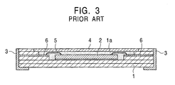
- Fig. 3 is a sectional view illustrating a conventional construction of one of the aforesaid SAW filters.
- the conventional SAW filter is primarily constructed of a multi-layer substrate (LTCC) 1, a SAW chip 2 mounted in a recession 1a of the multi-layer substrate 1, an end surface electrode 3 extending from a side surface of the multi-layer substrate 1 toward a bottom surface thereof, and a sealing plate 4 formed of a metal plate or the like connected at a position appropriate to cover the recession 1a of the multi-layer substrate 1.
- the multi-layer substrate 1 is composed of layered green sheets made of a low-temperature sintered ceramic material and fired at 1000°C or less.
- the multi-layer substrate 1 is mounted on a motherboard (not shown).
- the SAW chip 2 is formed of a piezoelectric substrate made of crystal or the like, a predetermined electrode pattern being formed on the surface thereof.
- the SAW chip 2 is connected to a lead pattern 6 by a bonding wire 5.
- the lead pattern 6 is in conduction with the end surface electrode 3, so that the SAW chip 2 can be electrically connected to an external circuit through the intermediary of the end surface electrode 3.
- the bottom surface of the SAW chip 2 is adhesively secured to the inner bottom surface of the recession 1a of the multi-layer substrate 1, and the recession 1a is filled with an inert gas, such as nitrogen.
- a SAW filter When a SAW filter is used as a transmitting filter for an antenna switching circuit, a transmitter signal amplified by a power amplifier is supplied to the SAW filter. Hence, the heat generated by the SAW chip 2 shown in Fig. 3 cannot ignored. More specifically, when an amplified transmitter signal is received, the SAW chip 2 generates considerable Joule heat; therefore, if transmission is continued for a prolonged time, the mere heat radiation primarily depending upon the sealing plate 4 can no longer sufficiently restrain a temperature rise in the SAW chip 2. For this reason, the conventional SAW filters used as transmitting filters have been posing a problem in that an undue temperature rise attributable to the heat generated by themselves adversely affects the characteristics of the SAW chip 2, making it difficult to achieve high reliability thereof.
- the present invention has been made with a view toward solving the problems with the prior art described above, and it is an object of the invention to provide a highly reliable SAW filter capable of restraining an undue temperature rise attributable to the heat generated by a SAW chip.
- the present invention provides a SAW filter having a substrate that has a recession and is mounted on a motherboard, a SAW chip mounted in the recession of the substrate, an external electrode that is provided on an external surface, including side surfaces, of the substrate, and is in conduction with the SAW chip, a sealing plate connected to the substrate to cover the recession, a metal conductor for radiating heat that is provided on a surface of the substrate at the opposite side from the sealing plate, a through hole provided in the substrate, one end thereof being connected to the metal conductor, wherein the other end of the through hole is connected to the SAW chip through the intermediary of a metal constituent.
- the Joule heat generated in the SAW chip is conducted to the metal conductor via the through hole, allowing the metal conductor to function as a heat sink.
- the metal conductor is mounted on a motherboard, the metal conductor side being the bottom surface, then the metal conductor is kept in contact with a conductor pattern (grounding pattern or the like) of the motherboard so as to dissipate heat through the intermediary of the conductor pattern.
- the SAW filter is mounted on the motherboard, the sealing plate side being the bottom surface, then the heat is dissipated directly from the metal conductor to the surrounding space.
- This arrangement eliminates the possibility of an undue temperature rise in the SAW chip due to its own generated heat, permitting stable performance to be always maintained.
- an adhesive layer formed of an electrically conductive adhesive agent is provided on the inner bottom surface of the recession of the substrate to secure the SAW chip to the substrate by the adhesive layer, and the other end of the through hole is connected to the adhesive layer.
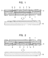
- Fig. 1 is a sectional view of a SAW filter according to a first embodiment, in which the components corresponding to those shown in Fig. 3 are assigned the same reference numerals.
- the SAW filter shown in Fig. 1 is constructed mainly of a multi-layer substrate 1 mounted on a motherboard 10, a SAW chip 2 mounted in a recession 1a of the multi-layer substrate 1, an end surface electrode 3 extending from a side surface to a bottom surface of the multi-layer substrate 1, a sealing plate 4 formed of a metal plate or the like that is connected to the upper surface of the multi-layer substrate 1 to cover the recession 1a, a metal conductor 7 provided on the bottom surface of the multi-layer substrate 1, and through holes 8 provided at a plurality of locations between the bottom surface of the SAW chip 2 and the metal conductor 7.
- the multi-layer substrate 1 is composed of layered green sheets made of a low-temperature sintered ceramic material and fired at 1000°C or less.
- the inner bottom surface of the recession 1a of the multi-layer substrate 1 is provided with an adhesive layer 9 formed of an electrically conductive adhesive agent.
- the electrically conductive adhesive layer 9 combines a function for securing the SAW chip 2 in the recession 1a and a function for transmitting the Joule heat generated in the SAW chip 2 to the through holes 8. More specifically, both upper and lower ends of the through holes 8 are connected to the adhesive layer 9 and the metal conductor 7, respectively. Hence, the Joule heat generated in the SAW chip 2 is transmitted from the through holes 8 to the metal conductor 7 through the intermediary of the adhesive layer 9.
- the recession 1a is filled with an inert gas, such as nitrogen.
- the SAW chip 2 is formed of a piezoelectric substrate made of crystal or the like, a predetermined electrode pattern being formed on the surface thereof.
- the SAW chip 2 is in conduction with an end surface electrode 3 through the intermediary of a bonding wire 5 and a lead pattern 6. Hence, mounting the SAW filter on the motherboard 10 and soldering the end surface electrode 3 to a solder land (not shown) of an external circuit will electrically connect the SAW chip 2 to the external circuit through the intermediary of the end surface electrode 3.
- the SAW filter having the construction discussed above is mounted on the motherboard 10, its metal conductor 7 side being the bottom surface, and the metal conductor 7 of the SAW filter is maintained in surface contact with a grounding pattern 11 formed on the motherboard 10 in advance.
- This arrangement causes the Joule heat generated in the SAW chip 2 to be transferred to the grounding pattern 11 of the motherboard 10 through the intermediary of the electrically conductive adhesive layer 9, the through holes 8, and the metal conductor 7 so as to be efficiently dissipated through the grounding pattern 11 having a large surface area.
- the heat is efficiently dissipated by making use of the grounding pattern 11 of the motherboard 10. This obviates the possibility of an undue temperature rise in the SAW chip 2 due to its own generated heat, permitting stable performance to be always maintained.
- Fig. 2 is a sectional view of a SAW filter according to a second embodiment, wherein the components corresponding to those shown in Fig. 1 are assigned the same reference numerals.
- This embodiment differs from the first embodiment in that the SAW filter is mounted on a motherboard 10 with its sealing plate side 4 as the bottom surface, the rest of the construction of this embodiment being basically the same.
- the sealing plate 4 side being the bottom surface, a metal conductor 7 is maintained exposed to outer space. This arrangement allows the Joule heat generated in the SAW chip 2 to be efficiently radiated to the surrounding space through the intermediary of the metal conductor 7.
- the present invention provides an advantage in that the Joule heat produced in a SAW chip is transmitted to a metal conductor via through holes, allowing the metal conductor to function as a heat sink capable of achieving efficient heat radiation. This makes it possible to provide a high-reliability SAW filter capable of restraining an undue temperature rise due to the heat generated in the SAW chip.
Landscapes
- Physics & Mathematics (AREA)
- Acoustics & Sound (AREA)
- Surface Acoustic Wave Elements And Circuit Networks Thereof (AREA)
Abstract
Description
Claims (2)
- A SAW filter comprising:wherein the other end of the through hole is connected to the SAW chip through the intermediary of a metal constituent.a substrate that has a recession and is mounted on a motherboard;a SAW chip mounted in the recession of the substrate;an external electrode that is provided on an external surface, including side surfaces, of the substrate, and is in conduction with the SAW chip;a sealing plate connected to the substrate to cover the recession;a metal conductor for radiating heat that is provided on a surface of the substrate at the opposite side from the sealing plate; anda through hole provided in the substrate, one end thereof being connected to the metal conductor,
- The SAW filter according to Claim 1, wherein an adhesive layer formed of an electrically conductive adhesive agent is provided on the inner bottom surface of the recession of the substrate so as to secure the SAW chip onto the substrate by the adhesive layer, and the other end of the through hole is connected to the adhesive layer.
Applications Claiming Priority (2)
| Application Number | Priority Date | Filing Date | Title |
|---|---|---|---|
| JP2002002500 | 2002-01-09 | ||
| JP2002002500A JP4173308B2 (en) | 2002-01-09 | 2002-01-09 | SAW filter |
Publications (2)
| Publication Number | Publication Date |
|---|---|
| EP1328063A2 true EP1328063A2 (en) | 2003-07-16 |
| EP1328063A3 EP1328063A3 (en) | 2004-09-29 |
Family
ID=19190753
Family Applications (1)
| Application Number | Title | Priority Date | Filing Date |
|---|---|---|---|
| EP03250066A Withdrawn EP1328063A3 (en) | 2002-01-09 | 2003-01-03 | Surface accoustic wave filter |
Country Status (5)
| Country | Link |
|---|---|
| US (1) | US6922119B2 (en) |
| EP (1) | EP1328063A3 (en) |
| JP (1) | JP4173308B2 (en) |
| KR (1) | KR100482888B1 (en) |
| CN (1) | CN1242552C (en) |
Families Citing this family (15)
| Publication number | Priority date | Publication date | Assignee | Title |
|---|---|---|---|---|
| US6992400B2 (en) * | 2004-01-30 | 2006-01-31 | Nokia Corporation | Encapsulated electronics device with improved heat dissipation |
| US7298231B2 (en) * | 2004-05-27 | 2007-11-20 | Kyocera Corporation | Surface acoustic wave device and communication apparatus |
| US7332986B2 (en) * | 2004-06-28 | 2008-02-19 | Kyocera Corporation | Surface acoustic wave apparatus and communications equipment |
| JP2006245990A (en) * | 2005-03-03 | 2006-09-14 | Matsushita Electric Ind Co Ltd | Surface acoustic wave device and manufacturing method thereof |
| JP4975377B2 (en) * | 2006-06-06 | 2012-07-11 | 太陽誘電株式会社 | Boundary acoustic wave element, resonator and filter |
| WO2008059674A1 (en) * | 2006-11-13 | 2008-05-22 | Murata Manufacturing Co., Ltd. | Acoustic boundary wave element, acoustic boundary wave device and method for fabricating them |
| US8338936B2 (en) * | 2008-07-24 | 2012-12-25 | Infineon Technologies Ag | Semiconductor device and manufacturing method |
| US8593016B2 (en) * | 2010-12-03 | 2013-11-26 | Sri International | Levitated micro-manipulator system |
| US10224260B2 (en) * | 2013-11-26 | 2019-03-05 | Infineon Technologies Ag | Semiconductor package with air gap |
| US10861627B2 (en) | 2015-04-20 | 2020-12-08 | Sri International | Microrobot and microrobotic train self-assembly with end-effectors |
| JP7117828B2 (en) * | 2017-06-13 | 2022-08-15 | 太陽誘電株式会社 | elastic wave device |
| KR102550176B1 (en) | 2017-11-09 | 2023-07-03 | 삼성전기주식회사 | Acoustic wave device and manufacturing method thereof |
| KR20200046535A (en) | 2018-10-25 | 2020-05-07 | 삼성전기주식회사 | Bulk acoustic filter device |
| CN109379056A (en) * | 2018-12-03 | 2019-02-22 | 全讯射频科技(无锡)有限公司 | A kind of SAW filter |
| CN109939875B (en) * | 2019-03-11 | 2021-01-05 | 哈尔滨工业大学(深圳) | Surface acoustic wave atomization chip, manufacturing method and device |
Family Cites Families (7)
| Publication number | Priority date | Publication date | Assignee | Title |
|---|---|---|---|---|
| JP3194540B2 (en) | 1992-07-13 | 2001-07-30 | 富士通株式会社 | Surface acoustic wave filter |
| JPH08307196A (en) * | 1995-05-08 | 1996-11-22 | Murata Mfg Co Ltd | Piezoelectric element mounting structure |
| US5786738A (en) * | 1995-05-31 | 1998-07-28 | Fujitsu Limited | Surface acoustic wave filter duplexer comprising a multi-layer package and phase matching patterns |
| JP3982876B2 (en) * | 1997-06-30 | 2007-09-26 | 沖電気工業株式会社 | Surface acoustic wave device |
| US6310422B1 (en) * | 1998-03-12 | 2001-10-30 | Matsushita Electric Industrial Co., Ltd. | Surface acoustic wave filter |
| SE519240C2 (en) | 1998-11-20 | 2003-02-04 | Volvo Personvagnar Ab | Combustion engine arrangements included a heat exchanger to adjust the temperature of exhaust gases to pass a NOx adsorbing catalyst |
| JP2000196407A (en) * | 1998-12-28 | 2000-07-14 | Tdk Corp | Surface acoustic wave device |
-
2002
- 2002-01-09 JP JP2002002500A patent/JP4173308B2/en not_active Expired - Fee Related
-
2003
- 2003-01-03 EP EP03250066A patent/EP1328063A3/en not_active Withdrawn
- 2003-01-07 US US10/338,459 patent/US6922119B2/en not_active Expired - Fee Related
- 2003-01-08 KR KR10-2003-0000940A patent/KR100482888B1/en not_active Expired - Fee Related
- 2003-01-09 CN CNB03101075XA patent/CN1242552C/en not_active Expired - Fee Related
Also Published As
| Publication number | Publication date |
|---|---|
| KR100482888B1 (en) | 2005-04-14 |
| US20030132517A1 (en) | 2003-07-17 |
| CN1431775A (en) | 2003-07-23 |
| CN1242552C (en) | 2006-02-15 |
| JP2003204244A (en) | 2003-07-18 |
| EP1328063A3 (en) | 2004-09-29 |
| US6922119B2 (en) | 2005-07-26 |
| JP4173308B2 (en) | 2008-10-29 |
| KR20030060807A (en) | 2003-07-16 |
Similar Documents
| Publication | Publication Date | Title |
|---|---|---|
| US6335669B1 (en) | RF circuit module | |
| CN101048863B (en) | Electronic component module and wireless communication device | |
| US7239222B2 (en) | High frequency circuit module | |
| US6922119B2 (en) | Surface acoustic wave filter adapted to restrain undue temperature rise | |
| JP3013831B2 (en) | MMIC package | |
| US6788171B2 (en) | Millimeter wave (MMW) radio frequency transceiver module and method of forming same | |
| EP1368858B1 (en) | Module and electronic device | |
| JP2003100937A (en) | High frequency module | |
| JP2005311230A (en) | Circuit module and circuit device using the circuit module | |
| JPH08335836A (en) | High frequency power amplifier circuit device | |
| US20060033207A1 (en) | Microwave-monolithic-integrated-circuit-mounted substrate, transmitter device for transmission only and transceiver device for transmission/reception in microwave-band communication | |
| GB2307596A (en) | Radio communications module | |
| JP2000133765A (en) | High frequency integrated circuit device | |
| JP4050186B2 (en) | Manufacturing method of electronic component mounting board | |
| JP4822900B2 (en) | Electronic component module | |
| JP3842887B2 (en) | Hybrid module | |
| KR100893028B1 (en) | Semiconductor device package and manufacturing method thereof | |
| JP4569590B2 (en) | Transceiver module | |
| JP4139165B2 (en) | Input / output terminal for semiconductor element storage package, semiconductor element storage package, and semiconductor device | |
| JP2003046180A (en) | Package for housing input / output terminals and optical semiconductor element, and optical semiconductor device | |
| JP5528484B2 (en) | Input / output terminal and optical semiconductor element storage package, and optical semiconductor device | |
| JP2004055570A (en) | High frequency package | |
| JP2003283168A (en) | Surface mount electronic components | |
| JP2004356342A (en) | Semiconductor element storage package and semiconductor device | |
| JP2004087617A (en) | I / O terminal and semiconductor element storage package and semiconductor device |
Legal Events
| Date | Code | Title | Description |
|---|---|---|---|
| PUAI | Public reference made under article 153(3) epc to a published international application that has entered the european phase |
Free format text: ORIGINAL CODE: 0009012 |
|
| AK | Designated contracting states |
Designated state(s): AT BE BG CH CY CZ DE DK EE ES FI FR GB GR HU IE IT LI LU MC NL PT SE SI SK TR |
|
| AX | Request for extension of the european patent |
Extension state: AL LT LV MK RO |
|
| PUAL | Search report despatched |
Free format text: ORIGINAL CODE: 0009013 |
|
| AK | Designated contracting states |
Kind code of ref document: A3 Designated state(s): AT BE BG CH CY CZ DE DK EE ES FI FR GB GR HU IE IT LI LU MC NL PT SE SI SK TR |
|
| AX | Request for extension of the european patent |
Extension state: AL LT LV MK RO |
|
| 17P | Request for examination filed |
Effective date: 20050108 |
|
| AKX | Designation fees paid |
Designated state(s): DE FR GB |
|
| 17Q | First examination report despatched |
Effective date: 20070403 |
|
| STAA | Information on the status of an ep patent application or granted ep patent |
Free format text: STATUS: THE APPLICATION IS DEEMED TO BE WITHDRAWN |
|
| 18D | Application deemed to be withdrawn |
Effective date: 20070814 |