The present invention relates to an electro-optical device capable of
efficiently transmitting light emitted or modulated by an electro-optical
element and to a method for manufacturing the electro-optical device. The
present invention also relates to electronic apparatuses and a circuit
substrate including the electro-optical device, and to a method for
manufacturing the circuit substrate.
Some electro-optical devices, such as liquid crystal devices and
organic EL (electroluminescence) devices, conventionally have a plurality
of circuit elements, electrodes, and liquid crystal or EL elements layered
on a member. For example, an organic EL device has luminescent elements,
each including electrode layers serving as an anode and a cathode and a
luminescent layer containing a luminescent material disposed between the
electrode layers. The organic EL device uses a phenomenon in which holes
injected from the anode side and electrons injected from the cathode side
are recombined in the luminescent layer capable of emitting light and the
luminescent layer emits light when an excited state is deactivated.
Since the electro-optical devices generally comprises a plurality of
material layers including an electro-optical layer, light emitted or
modulated in the electro-optical devices decays while traveling to the
outside through the material layers. Consequently, these devices cannot
efficiently emit the light.
Accordingly, an object of the present invention is to provide an
electro-optical device having an increased efficiency of light emission to
the outside and a high visibility, and to provide a method for manufacturing
the electro-optical device, a circuit substrate, and a method for
manufacturing the circuit substrate.
To this end, the present invention is directed to an electro-optical
device having a plurality of material layers including an electro-optical
element layer having electro-optical elements. The electro-optical device
comprises a plurality of material layers layered in the direction of light
emission from the electro-optical elements. The material layers include a
surface material layer disposed at the outermost surface thereof and a
low-refractive-index layer disposed between the surface material layer and
the electro-optical element layer. The low-refractive-index layer has a
refractive index lower than that of the surface material layer.
The "light emission from the electro-optical elements" here refers to
not only light emitted by the electro-optical elements but also transmitted
or reflected light modulated by the electro-optical elements. The "surface
material layer disposed at the outermost surface thereof" refers to a material
layer in contact with the outside.
According to the present invention, light omitted from electro-optical
elements passes through the low-refractive-index material layer having a
refractive index lower than that of the surface material layer and enters
the surface material layer. Light entering the low-refractive-index layer
at an angle more than or equal to the critical angle is refracted in a direction
forming an angle less than or equal to the critical angle at the interface
with the surface material layer. Thus the light is deviated from total
reflection conditions to be emitted to the outside. Thus, light emission
efficiency can be increased to achieve an enhanced visibility. Also, there
is a strong correlation between the refractive index and the dielectric
constant. By setting the refractive index of some material layers to be low,
low-dielectric-constant layers can be provided.
The electro-optical elements may be liquid crystal elements,
electrophoretic elements, or electron-emissive elements. In the structure
of the electro-optical device described above, however, it is particularly
preferable that the electro-optical elements be luminescent elements. The
luminescent elements may be LED (light-emitting diode) elements, LD (laser
diode) elements, EL (electroluminescent) elements, or luminescent elements
including electron-emissive elements.
In the electro-optical device, by allowing the low refractive later to
serve as an insulating interlayer, the emission efficiency of light passing
through the insulating interlayer can be increased.
Since there is a strong correlation between the refractive index and
the dielectric constant, capacitance generated between the wires can be
advantageously reduced when conductive members, such as the wires and
electrodes, are insulated with the insulating interlayer. Thus, an
electro-optical device having a high light emission efficiency and capable
of high-speed operation can be achieved.
Preferably, the refractive index of the low-refractive-index layer is
1.5 or less, and more preferably 1.2 or less.
The low-refractive-index material may be aerogel, porous silica,
magnesium fluoride or a material containing magnesium fluoride, a gel in which
magnesium fluoride particles are dispersed, a fluoropolymer or a material
containing the fluoropolymer, or a porous polymer having a side chain
structure. Also, the low-refractive-index material may comprise a
predetermined material containing at least either inorganic particles or
organic particles.
The electro-optical elements may be organic electroluminescent
elements. The organic electroluminescent elements have various advantages
in that, for example, they can be operated at low voltage and have an
angle-dependent visibility lower than that of liquid crystal elements.
The electro-optical device may include active elements. Thus, active
driving can be achieved. The active elements may be, for example, transistors,
such as thin-film transistors, or thin-film diodes.
The present invention is also directed to a method formanufacturing an
electro-optical device. The method includes the steps of disposing thin-film
transistors on a first base material; and forming a low-refractive-index
layer on a second base material including the thin-film transistors and the
first base material.
The present invention is also directed to a circuit substrate comprising
a member and a plurality of material layers on the member. The plurality
of material layers include at least one low-refractive-index layer formed
of a low-refractive-index material having a refractive index lower than that
of the member.
In the circuit substrate, the plurality of material layers include at
least one insulating interlayer formed of the low-refractive-index material.
Preferably, the refractive index of the low-refractive-index layer is
1.5 or less, and more preferably 1.2 or less.
The low-refractive-index material may be light-transmissive porous
material, aerogel, porous silica, magnesium fluoride, a fluoropolymer, or
a porous polymer. Alternatively, the low-refractive-index material may
comprise a predetermined material containing at least either inorganic
particles or organic particles, or a gel in which magnesium fluoride particles
are dispersed.
In this instance, the circuit substrate may include active elements.
The active elements may be transistors.
The present invention is also directed to a method for manufacturing
a circuit substrate. The method includes the steps of disposing transistors
on a first base material; and forming a low-refractive-index layer on a second
base material including the transistors and the first base material.
The present invention is also directed to an electronic apparatus
including the electro-optical device or the circuit substrate described
above.
According to the present invention, an electronic apparatus having a
display capable displaying high-quality, bright images can be achieved.
Embodiments of the present invention will now be described by way of
further example only and with reference to the accompanying drawings, in
which:-
An electro-optical device of the present invention will now be
illustrated with reference to Figs. 1, 2, and 3. Figs 1 and 2 show an
electro-optical device of the present invention, using an active matrix
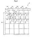
display device including organic EL elements. Fig. 1 is a circuit diagram
of an entire circuit substrate and Fig. 2 is an enlarged plan view of a pixel
in which an opposing electrode and an organic electroluminescent element
acting as a luminescent element shown in Fig. 1 are omitted.
In the embodiment, a display device including organic
electroluminescent elements (hereinafter referred to as "EL element", if
necessary) will be illustrated. However, the present invention may be applied
to other types of display devices including liquid crystal elements,
electrophoretic elements, or electron-emissive elements, or including other
types of luminescent elements, such as LEDs (light emitting diodes) elements
and LDs (laser diodes).
As shown in Fig. 1, the organic electroluminescent display device S1
(hereinafter referred to as an "organic EL display device", if necessary)
includes a member, a plurality of scanning lines 131 disposed on the member,
a plurality of data lines 132 extending so as to intersect the scanning lines
131, and a plurality of common power-supply lines 133 extending alongside
the data lines 132. Pixels (pixel area elements) AR are arranged
corresponding to the intersections of the scanning lines 131 and the data
lines 132.
The data lines 132 are electrically connected to a data line driving
circuit 90 including at least one selected from the group consisting of a
shift register, a level shifter, a video line, a D/A converter, a decoder,
a latch circuit, and an analog switch.
On the other hand, the scanning lines 131 are electrically connected
to a scanning line driving circuit 80 including at least one selected from
the group consisting of a shift register, a level shifter, and a decoder.
In this embodiment, both the data line driving circuit 90 and the
scanning line driving circuit 80 are disposed on the member. However, whether
the data line driving circuit 90 and the scanning line driving circuit 80
are disposed on the member or outside the member is determined as required.
As shown in Fig. 1, each pixel area AR includes: a first thin-film
transistor 22 having a gate electrode to which scanning signals are
transmitted through the corresponding scanning line 131; and a hold capacitor
cap for holding an image signal supplied from the corresponding data line
132 through the first thin-film transistor 22. The pixel area AR also
includes: a second thin-film transistor 24 having a gate electrode to which
the image signals held in the hold capacitor cap is transmitted; and a pixel
electrode 23 to which driving current is transmitted from the corresponding
common power supply line 133 when the pixel electrode 23 is electrically
connected to the common power supply line 133 with the second thin-film
transistor 24. A luminescent element 3 is also disposed between the pixel
electrode (anode) 23 and an opposing electrode (cathode) 222. Instead of EL
(electroluminescent) elements, LEDs (light-emitting diodes) or LDs (laser
diodes) may be used as the luminescent element 3.
When the first thin-film transistor 22 is activated according to a
scanning signal supplied through the scanning line 131, electric charge
corresponding to a data signal supplied through the data line 132 is held
in the hold capacitor cap, and thus the conduction state of the second
thin-film transistor 24 is determined depending on the state of the hold
capacitor cap. A current flows from the common power supply line 133 to the
pixel electrode 23 through the second thin-film transistor 24 and to the
opposing electrode 222 through a luminescent layer 60. Thus, the luminescent
layer 60 emits light depending on the amount of the current.
The plan structure of the pixel AR will now be described with reference
to Fig. 2. Fig. 2 is an enlarged plan view of one of the pixels shown in
Fig. 1 in which the opposing electrode and the organic electroluminescent
element are omitted. As shown in Fig. 2, the pixel electrode 23 is disposed
in rectangular shape when viewed from above, and all sides of the pixel
electrode 23 are surrounded by the corresponding data line 132, common power
supply line 133, and scanning line 131 and a scanning line for another pixel
electrode not shown in the drawing. The shape of the pixel electrode is not
limited to being rectangular, but may be circular or oval. If the material
layers defining the El element including the luminescent layer are formed
of liquid materials by, for example, an ink jet technique, a circular or oval
pixel electrode not having corners helps form uniform material layers.
The sectional structure of the organic EL display device will now be
described with reference to Fig. 3. Fig. 3 is a sectional view taken along
line A-A in Fig. 2.
The organic EL display device shown in Fig. 3 is a so-called back
emission type in which light is emitted from the member 2 side having the
thin-film transistors (TFTs). Accordingly, in this embodiment, the member
2 serves as the outermost material layer through which light from the
luminescent elements 3 passes to the outside. If another material layer is
layered on the surface of the member 2, that layer serves as the outermost
material layer.
As shown in Fig. 3, the back emission organic type organic EL display
device S1 includes the member 2; an transparent anode (pixel electrode) 23
formed of indium tin oxide (ITO) or the like; a luminescent element 3 disposed
on the anode 23; a cathode (opposing electrode) 222 overlying the anode 23
with the luminescent element 3 therebetween; and a thin-film transistor
(hereinafter referred to as a TFT) 24 serving as an energization controller
for controlling energization of the pixel electrode 23. In addition, a
sealing layer 20 is disposed on the cathode 222. The cathode 222 is formed
of at least one metal selected from the group consisting of aluminium (Al),
magnesium (Mg), gold (Au), silver (Ag), and calcium (Ca). The cathode 222
may be an alloy film or a laminate formed of those metals. The TFT 24 operates
according to operation instructing signals from the scanning line driving
circuit 80 and the data line driving circuit 90 to control the energization
of the pixel electrode 23.
The luminescent element 3 is substantially composed of a hole transport
layer 70 capable of transporting holes from the anode 23; a luminescent layer
60 containing an organic EL material which is one of electro-optical
materials; and an electron transport layer 50 disposed on the upper surface
of the luminescent layer 60. The cathode (opposing electrode) 222 is disposed
on the upper surface of electron transport layer 50.
The TFT 24 is disposed above the surface of the member 2 with a protective
underlayer 281 mainly containing SiO2 therebetween. The TFT 24 includes a
silicon layer 241 disposed on the protective underlayer 281, a gate insulating
layer 282 disposed on the protective underlayer 281 so as to cover the silicon
layer 241, a gate electrode 242 on the upper surface of the gate insulating
layer 282, opposing the silicon layer 241, a first insulating interlayer 283
disposed on the gate insulating layer 282 so as to cover the gate electrode
242, a source electrode 243 connected to the silicon layer 241 through a
contact hole formed in the gate insulating layer 282 and the first insulating
inter layer 283, a drain electrode 244 opposing the source electrode 243 with
the gate electrode 242 therebetween and connected to the silicon layer 241
through a contact hole formed in the gate insulating layer 282 and the first
insulating interlayer 283, and a second insulating interlayer 284 disposed
on the first insulating interlayer 283 so as to cover the source electrode
243 and the drain electrode 244.
The pixel electrode 23 is disposed on the upper surface of the second
insulating interlayer 284, and is connected to the drain electrode 244 through
a contact hole 23a formed in the second insulating interlayer 284. Also,
a third insulating layer (bank layer) 221 formed of a synthetic resin or the
like is disposed between the cathode 222 and the region of the second
insulating interlayer 284 in which the luminescent element (EL element) 3
are not formed.
The drain electrode 244 may be provided with a TFT protection layer on
the surface thereof. The material of the protection layer may be an insulating
film containing silicon (preferably a silicon nitride oxide film or a silicon
nitride film). This protection layer serves to protect the TFT 24 from metal
ions and water. Specifically, the protection layer prevents movable ions
such as metal ions from entering the TFT 24.
If the protection layer has the effect of dissipating heat, it can
advantageously prevent thermal degradation of the luminescent element. If
the luminescent element is formed of an organic material, however, the
luminescent element is degraded by oxygen. Therefore, it is preferable that
the protection layer be not formed of an insulating film easily releasing
oxygen.
Such a light-transmissive insulating film capable of preventing
transmission of movable ions and having the effect of releasing heat may
contain at least one element selected from the group consisting of B (boron),
C (carbon), and N (nitrogen) and at least one element selected from the group
consisting of Al (aluminium), Si (silicon), and P(phosphorus). For example,
nitrides containing aluminium such as aluminium nitride (AlxNy), carbide
containing silicon such as silicon carbide (SixCy), nitrides containing
silicon such as silicon nitride (SixNy), nitrides containing boron such as
boron nitride (BxNy), and phosphides containing boron such as boron phosphide
(BxPy) may be used. Oxides containing aluminium such as aluminium oxide (AlxOy)
are also preferable because it is light-transmissive and has a thermal
conductivity of 20 Wm-1K-1. These materials can prevent the entry of water
as well as having the above-described effects.
Those compounds may be combined with other elements. For example,
aluminium nitride oxide expressed by AlNxOy formed by adding nitrogen to
aluminium oxide may be used. This material also has the effects of releasing
heat and of preventing the entry of water and movable ions.
Other insulating films containing Si, Al, N, O, and M may be used,
wherein M represents at least one of rare earth elements, and preferably at
least one element selected from the group consisting of Ce (cesium), Yb
(ytterbium), Sm (samarium), Er (erbium), Y (yttrium), La (lanthanum), Gd
(gadolinium), Dy (dysprosium), and Nd (neodymium). These materials also have
the effects of releasing heat and of preventing the entry of water and movable
ions.
Alternatively, carbon films containing at least a diamond thin film or
an amorphous carbon film (particularly having characteristics similar to
diamond, referred to as diamond-like carbon or the like) may be used. These
films have extremely high thermal conductivity and is, therefore, useful for
a cooling layer. However, a film having a large thickness has a brown tinge
and reduces the transmittance thereof. It is desired that the film have a
thickness as small as possible (preferably in the range of 5 to 100 nm).
Since the protection layer is intended to protect the TFT from movable
ions and water, it is preferable that the material of the protection layer
does not degrade this effect. Although a thin film containing the
above-described material having the effect of dissipating heat may be used
singly as the protection layer, it is advantageous to layer the thin film
and an insulating film capable of preventing the transmission of movable ions
and water (typically a silicon nitride (SixNy) film or silicon nitride oxide
(SiOxNy) film).
The region of the silicon layer 241 opposing the gate electrode 242 with
the gate insulating layer 282 therebetween is a channel region. The source
side of the channel region in the silicon layer 241 is a source region. On
the other hand, the drain side of the channel region is a drain region. The
source region is connected to the source electrode 243 through a contact hole
formed in the gate insulating layer 282 and the first insulating interlayer
283. The drain region is connected to the drain electrode 244 formed in the
same layer as the source electrode 243 through a contact hole formed in the
gate insulating layer 282 and the first insulating interlayer 283. The pixel
electrode 23 is connected to the drain region of the silicon layer 241 through
the drain electrode 244.
In this embodiment, since light emitted from the luminescent layer 60
passes through the member 2 having the TFT 24 to the outside (back emission
type), the member 2 is formed of a light-transmissive, transparent or
translucent material, such as transparent glass, quartz, sapphire, or a
transparent synthetic resin, such as polyester, polyacrylate, polycarbonate,
or polyether ketone. In particular, soda-lime glass is advantageously used
as a constituent of the member. In use of soda-lime glass, preferably, the
member is coated with silica to protect the soda-glass from acids and alkalis
and to improve the uniformity of the member.
The member may be provided with a color filter layer, a color-converting
layer containing a luminescent material, or a dielectric substance reflection
layer to control the color of luminescence.
If emitted light passes through the side opposite to the member 2 having
the TFT 24 to the outside (top emission type), the member 2 is not necessary
to be transparent and may be formed of ceramics such as alumina, metallic
sheets such as stainless steel subjected to surface oxidation or other surface
insulation treatments, thermosetting resins, or thermoplastic resins.
When the protective underlayer 281 is formed, the member 2 is subjected
to plasma CVD using TEOS (tetraethoxysilane) or oxygen gas as a material to
deposit a silicon nitride film acting as the protective underlayer 281 at
a thickness of about 200 to 500 nm.
When the silicon layer 241 is formed, the member 2 is, first, heated
to about 350°C and the protective underlayer 281 is subjected to plasma CVD
or ICVD to deposit an amorphous silicon film at a thickness of about 30 to
70 nm. Next, the amorphous silicon film is crystallized by laser annealing,
flash heating, or solid phase deposition to form a crystallized polysilicon
layer. The laser annealing is performed using a line beam emitted from an
excimer laser, having a length of 400 mm and an output intensity of, for
example, 200 mJ/cm2. The line beam is scanned such that the area corresponding
to 90% of the leaser peak intensity in the width direction of the line beam
overlaps targeted regions. Next, the polysilicon layer is subjected to
patterning by photolithography to form an island-shaped silicon layer 241.
The silicon layer 241 includes the channel region and the source and
drain regions of the second thin-film transistor 24 shown in Fig. 1 and, in
a sectional view at a different position, also includes a channel region and
source and drain regions of the first thin-film transistor 22. Specifically,
these two transistors 22 and 24 are formed at one time through the same
procedure. As for the transistors, therefore, only the second thin-film
transistor 24 will be described and the description of the first thin-film
transistor 22 is omitted.
When the gate insulating layer 282 is formed, the surface of the silicon
layer 241 is subjectad to plasma CVD using TEOS or oxygen gas as a material
to deposit a silicon oxide or silicon nitride film at a thickness of about
60 to 150 nm.
In order to form the gate electrode 242, a conductive film containing
a metal, such as aluminium, tantalum, molybdenum, titanium, or tungsten, is
deposited on the gate insulating layer 282 by sputtering and is subsequently
subjected to patterning.
In order to form the source region and the drain region in the silicon
layer 241, after forming the gate electrode 242, phosphorus ions are implanted
using the gate electrode 242 as a patterning mask. As a result, a high
concentration dopant is introduced into the gate electrode 242 in a
self-alignment manner and, thus, the source region and the drain region are
formed in the silicon layer 241. The region where the dopant is not introduced
is the channel region.
The first insulating interlayer 283 is formed of a material having a
refractive index lower than that of the member 2, on the upper surface of
the gate insulating layer 282.
The first insulating interlayer 283 may be a silicon oxide film, a
nitride film, a porous silicon oxide (SiO2) film, or the like. The first
insulating interlayer 283 formed of a porous SiO2 film is deposited by CVD
(chemical vapor deposition) using Si2H6 and O3 as a reaction gas. These gases
help form large SiO2 particles in a gas phase, and these large particles are
deposited on the gate insulating layer 282. As a result, the first insulating
interlayer 283 has many pores therein and becomes a porous film. The resulting
porous first insulating interlayer 283 has a low refractive index,
consequently increasing the efficiency of light emission to the outside.
Preferably, the density of the porous layer having a low refractive
index is 0.4 g/cm3 or less.
The refractive index of the first insulating interlayer 283 acting as
a low-refractive-index layer is 1.5 or less, and preferably 1.2 or less.
The surface of the first insulating interlayer 283 may be subjected to
H (hydrogen) plasma treatment. As a result, dangling bonds of Si-O bonds
on the surfaces defining the pores are replaced with Si-H bonds and, thus,
the non-hygroscopicity of the film is improved. The first insulating
interlayer 283 subjected to the plasma treatment may be provided with another
SiO2 layer on the surface thereof.
When the first insulating interlayer 283 is deposited by CVD, Si2H6 +
O2, Si3H8 + O3, or Si3H8 + O2 may be used as the reaction gas, instead of Si2H6
+ O3. In addition to these gases, a reaction gas containing B (boron) or F
(fluorine) may be used.
When the first insulating interlayer 283 is formed of a porous film,
by depositing the porous SiO2 film and a normal SiO2 film formed by
reduced-pressure chemical vapor deposition, the film characteristics of the
resulting porous first insulating interlayer 283 can be stable. In order
to deposit these films, a plasma is generated intermittently or periodically
in an atmosphere of SiH4 and O2 gases under a reduced pressure. Specifically,
in order to form the fist insulating interlayer 283, the member 2 is placed
in a predetermined chamber maintained at a temperature of, for example, 400°C,
and a RF voltage is applied to the chamber using SiH4 and O2 as the reaction
gas. In this process, while the flow rate of SiH4 and O2 gases are constant,
the RF voltage is periodically applied to the chamber at intervals of 10
seconds. Accordingly, the plasma is generated and destroyed in a cycle of
10 seconds by using a plasma changing with time, a reduced-pressure CVD
process and a plasma CVD process under a reduced pressure can be repeated
in one chamber. Also, by repeating the reduced-pressure CVD and the plasma
CVD under a reduced pressure, the resulting SiO2 film has many pores therein.
Hence, the first insulating interlayer 283 becomes porous.
The first insulating interlayer 283 may be formed of aerogel. Aerogel
is a light-transmissive porous material having an ultrastructure, and is
prepared by subjecting a metal alkoxide to sol-gel reaction and subsequently
by supercritical-drying the resulting wet gel. The types of aerogel include
silica aerogel and alumina-based aerogel. Silica aerogel has 90% of pores
relative to the volume, and the other part of the volume is constituted of
fine SiO2 particles having a size of tens of nanometers aggregated in a
dendritic manner. Since the particle size is smaller than wavelengths of
light, the silica aerogel is light-transmissive and has a refractive index
of 1.2 or less. The refractive index can be controlled by varying the pore
ratio. The refractive indexes of glass and quartz, which may be a constituent
of the member 2, are 1.54 and 1.45, respectively.
The silica aerogel is prepared by a sol-gel technique through a wet
gel-preparing step, a wet gel-ageing step, and a supercritical drying step
of drying the wet gel to obtain aerogel. In supercritical drying, liquid
in a jelly-like gel composed of a solid phase and a liquid phase is replaced
with a supercritical fluid and is thus removed. The supercritical drying
is suitable for drying gel without shrinkage, and results in an aerogel having
a high pore ratio.
For example, when the first insulating interlayer 283 is formed of
silica aerogel, the gate insulating layer 282 is coated with a wet gel, which
is an aerogel material, by spin coating or the like and supercritical drying.
By performing the supercritical drying, the solvent in the wet gel is replaced
with a supercritical fluid and removed. Exemplary supercritical fluids
include carbon dioxide (CO2), alcohols such as methanol and ethanol, NH3, H2O,
N2O, methane, ethane, ethylene, propane, pentane, isopropyl alcohol, isobutyl
alcohol, cyclotrifluoromethane, monofluoromethane, and cyclohexanol.
When each low-refractive-index layer (each insulating layer) is formed
of silica aerogel, a wet gel is applied onto a base material by spin coating,
followed by supercritical drying. In this instance, the wet gel may contain
a synthetic resin (organic substance). The synthetic resin is
light-transmissive and has a thermal degeneration point higher than the
critical temperature of the supercritical fluid. For example, when an alcohol
is used as the supercritical fluid, the synthetic resin must be
light-transmissive and have a thermal degeneration point higher than the
critical temperature of the alcohol. Such resins include hydroxylpropyl
cellulose (HPC), polyvinyl butyral (PVB), and ethyl cellulose (EC) (PVB and
EC are soluble in alcohol, but insoluble in water). If ether is used as the
solvent, preferably, polyethylene chloride or the like is used as the resin.
If CO2 is used as the solvent, preferably, HPC or the like is used as the resin.
Instead of silica aerogel, low-refractive-index layers may be formed
of an alumina-based aerogel or other light-transmissive, porous materials
having a refractive index lower than that of the member 2. Preferably, the
density of the porous material (aerogel) is 0.4 g/cm3 or less.
The low-refractive-index layers are not needed to be porous, and may
be formed of a light-transmissive polymeric adhesive having a refractive
index lower than that of the member 2, such as an epoxy adhesive (refractive
index: 1.42) or an acrylic resin (refractive index: 1.43). Since the
resulting layer has a refractive index lower than that of the member 2 even
if these adhesives are used singly, the efficiency of light emission to the
outside can be increased.
Also, the low-refractive-index layers may be formed of porous silica,
magnesium fluoride (refractive index: 1.38), or a material containing
magnesium fluoride. A low-refractive-index layer of magnesium fluoride can
be formed by sputtering. The low-refractive-index layers may be formed of
a gel in which magnesium fluoride particles are dispersed. Also, the
low-refractive-index layers may be formed of a fluoropolymer or a material
containing a fluoropolymer, such as perfluoroalkyl polyether,
perfluoroalkylamine, or a mixture of perfluoroalkyl polyether and
perfluoroalkylamine.
In addition, the low-refractive-index layers may be formed of a material
containing a predetermined polymer binder and a soluble or dispersive
fluorocarbon having a low refractive index.
Exemplary polymer binders include polyvinyl alcohol, polyacrylic acid,
polyvinylpyrrolidone, sodium polyvinylsulfonate, polyvinylmethyl ether,
polyethylene glycol, poly(α-(trifluoromethyl)acrylic acid), polyvinyl
methyl ether-maleic anhydride copolymer, polyethylene glycol-propylene
glycol copolymer, and polymethacrylic acid.
Exemplary fluorocarbons include ammonium perfluorooctanoate,
tetramethylammonium perfluorooctanoate, ammonium perfluoroalkylsulfonates
having a carbon number of 7 or 10, tetramethylammonium
perfluoroalkylsulfonates having a carbon number of 7 or 10, fluorinated
quaternary alkylammonium iodides, and perfluoroadipic acid, and
perfluoroadipic acid quaternary ammonium salts.
Since it is advantageous to introduce pores into the
low-refractive-index layer, particles may be used, instead of the
above-described aerogel, to form pores acting as micro voids among or in the
particles. As the particles, inorganic or organic particles may be used for
the low-refractive-index layers.
Inorganic particles are, preferably, amorphous. The inorganic
particles are constituted of, preferably, a metal oxide, a nitride, a sulfide,
or a halide, more preferably a metal oxide or a metal halide, and most
preferably a metal oxide or metal fluoride. Preferred metal elements include
Na, K, Mg, Ca, Ba, Al, Zn, Fe, Cu, Ti, Sn, In, W, Y, Sb, Mn, Ga, V, Nb, Ta,
Ag, Si, B, Bi, Mo, Ce, Cd, Be, Pb, and Ni, and more preferably Mg, ca, B,
and Si. An inorganic compound containing two types of metals may be used.
Particularly preferred inorganic compound is silicon dioxide, that is,
silica.
The micro voids in the inorganic particles are formed by cross-linking
silica molecules of the particles. By cross-linking the silica particles,
the volume is reduced and thus the particles become porous. The (porous)
inorganic particles having micro voids can be directly prepared as a
dispersoid by a sol-gel process (disclosed in Japanese Unexamined Patent
Application Publication No. 53-112732 and Japanese Examined Patent
Application Publication No. 57-9051) or deposition (disclosed in APPLIED
OPTIC, 27, pp 3356(1988)) The dispersoid may be obtained by preparing powder
by drying and sedimentation and subsequently by mechanical pulverization.
Alternatively, commercially available porous inorganic particles (for
example, silica dioxide sol) may be used. In order to form the
low-refractive-index layers, the inorganic particles having micro voids are,
preferably, dispersed in a suitable disperse medium. Preferably, preferred
disperse media include water, alcohols such as methanol, ethanol, and
isopropyl alcohol, and ketones such as methyl ethyl ketone and methyl isobutyl
ketone.
If organic particles are used, preferably, they are also amorphous.
Preferably, the organic particles are polymer particles synthesized by
polymerization (for example, emulsion polymerization) of monomers.
Preferably, the organic polymer particles contain elementary fluorine.
Exemplary monomers containing elementary fluorine used for synthesizing a
fluorine-containing polymer include: fluoroolefins such as fluoroethylene,
vinylidene fluoride, tetrafluoroethylene, hexafluoropropylene, and
perfluoro-2,2-dimethyl-1,3-dioxol; fluorinated alkylesters of acrylic acid
or methacrylic acid; and fluorinated vinyl ethers. A copolymer of a monomer
containing fluorine and a monomer not containing fluorine may be used.
Exemplary monomers not containing fluorine include olefins such as ethylene,
propylene, isoprene, vinyl chloride, and vinylidene chloride; acrylic esters
such as methyl acrylate, ethyl acrylate, and 2-ethylhexyl acrylate;
methacrylic esters such as methyl methacrylate, ethyl methacrylate, and butyl
methacrylate; styrenes such as styrene, vinyltoluene, and α-methylstyrene;
vinyl ethers such as methyl vinyl ether; vinyl esters such as vinyl acetate
and vinyl propionate; acrylamides such as N-tert-butylacrylamide and
N-cyclohexylacrylamide; methacrylamides; and acrylonitriles.
The micro voids in the organic particles are formed by cross-linking
polymers of the particles. By cross-linking the polymer molecules, the volume
is reduced and thus the particles become porous. In order to cross-link the
polymer molecules of the particles, preferably, monomers used to synthesize
the polymer include 20 mol% of polyfunctional monomer. The content of the
polyfunctional monomer is preferably in the range of 30 to 80 mol%, and most
preferably in the range of 35 to 50 mol%. Exemplary polyfunctional monomers
include dienes, such as butadiene and pentadiene; esters of polyhydric
alcohol and acrylic acid, such as ethylene glycol diacrylate, 1,4-cyclohexane
diacrylate, and dipentaerythritol hexacrylate; esters of polyhydric alcohol
and methacrylic acid, such as ethylene glycol dimethacrylate,
1,2,4-cyclohexane tetramethacrylate, and pentaerythritol
tetramethacrylate; divinyl compounds, such as divinylcyclohexane,
1,4-divinylbenzene; divinylsulfone; bisacrylamides, such as methylene
bisacrylamide; and bismethacrylamides. Micro voids among particles can be
formed by piling at least two particles.
The low-refractive-index layers may be formed of a material having pores
and containing inorganic particles. In this instance, the
low-refractive-index layers are formed by coating, and then the layer is
subjected to activated gas treatment in which gas is removed from the layer
to form pores. The low-refractive-index layers may be formed of a particle
mixture containing at least two types of ultrafine particles (for example,
MgF2 and SiO2) whose mixture ratio is varied in the thickness direction. By
varying the mixture ratio, the refractive index is also varied. The ultrafine
particles are adhered to each other with SiO2 produced by the thermal
decomposition of ethyl silicate. Also, in the thermal decomposition of ethyl
silicate, the ethyl group burns to produce carbon dioxide and water vapor.
By removing the carbon dioxide and the water vapor from the layer, pores are
formed among the ultrafine particles. The low-refractive-index layers may
contain a binder and inorganic particles constituted of porous silica, or
it may be formed by piling at least two particles constituted of a polymer
containing fluorine to form pores among the particles.
Some branch structure can increase the pore ratio. For example,
polymers having a branch structure, such as dendrimer, can be formed into
a low-refractive-index layer.
The refractive index of the resulting low-refractive-index layer formed
of the above-described material is preferably 1.5 or less, and more preferably
1.2 or less. If the member 2 is formed of quartz, whose refractive index
is 1.45, or glass, whose refractive index is 1.54, the low-refractive-index
layer has a refractive index lower than that of the member 2.
In order to form the source electrode 243 and the drain electrode 244,
first, the first insulating interlayer 283 is subjected to patterning by
photolithography to form contact holes for the source electrode and the drain
electrode. Next, a conductive layer is formed of a metal, such as aluminium,
chromium, or tantalum, so as to cover the first insulating interlayer 283.
Then, the regions of the conductive layer where the source and drain
electrodes are to be formed are covered with a patterning mask and the
conductive layer is subjected to patterning. Thus the source electrode 243
and the drain electrode 244 are formed.
The second insulating interlayer 284 is formed of a material having a
low refractive index on the first insulating interlayer 283, as in the first
insulating intarlayer 283. After forming the second insulating interlayer
284, a contact hole 23a is formed in the region of the second insulating
interlayer 284 corresponding to the drain electrode 244.
The anode 23 connected to the luminescent element 3 is formed of a
transparent electrode material, such as ITO, SnO2 doped with fluorine, ZnO,
or polyamine, and is connected to the drain electrode 244 of the TFT 24 through
the contact hole 23a. In order to form the anode 23, the above-described
transparent electrode material is deposited on the upper surface of the second
insulating interlayer 284, followed by being patterned.
The third insulating layer (bank layer) 221 is formed of a synthetic
resin such as an acrylic resin or a polyimide resin. The third insulating
layer 221 is formed after the anode 23 has been formed. Specifically, a resist,
such as an acrylic resin or a polyimide resin, is dissolved in a solvent and
this solution is applied to form an insulating layer by spin coating, dip
coating, or the like. Any material can be used for the insulating layer,
as long as it is insoluble in solvents for an ink described later and easy
to pattern by etching. Furthermore, the insulating layer is simultaneously
etched by photolithography or the like to form an opening 221a. Thus the
third insulating layer having the opening 221a is completed.
At this point, the third insulating layer 221 is divided into a lyophilic
(ink-philic) region and a liquid-repellent (ink-repellent) region. In this
embodiment, these regions are formed in a plasma treatment process. The
plasma treatment process includes a preheating step, the step of giving
ink-philic characteristics to the side surface of the opening 221a and the
surface of the pixel electrode 23, the step of giving ink-repellent
characteristics to the upper surface of the third insulating layer 221, and
a cooling step.
Specifically, a base material (the member 2 having the third insulating
layer and other layers) is heated to a predetermined temperature (for example,
about 70 to 80°C), and subsequently, in the step of giving ink-philic
characteristics, the base material is subjected to plasma treatment (O2 plasma
treatment) in an atmosphere of air, using oxygen as a reaction gas. Then,
in the step of giving ink-repellent characteristics, plasma treatment (CF4
plasma treatment) is performed in an atmosphere of air, using
tetrafluoromethane as a reaction gas. The base material heated for the plasma
treatments is cooled down to room temperature and, thus, the ink-philic and
ink-repellent characteristics are given to the specific regions separately.
The surface of the pixel electrode 23 is affected to some extent by the CF4
plasma treatment. However, the material of the pixel electrode 23, such as
ITO, does not have affinity to fluorine, and consequently, hydroxy groups
introduced in the step of giving ink-philic characteristics are not replaced
with fluoride groups and the ink-philic characteristics are thus maintained.
In the embodiment, both the first insulating interlayer 283 and the
second insulating interlayer 284 have a low refractive index. However, it
is not necessary that both refractive indexes are low, and only one of the
insulating interlayers may serve as a low-refractive-index layer.
In addition to the first and second insulating interlayers 283 and 284,
the gate insulating layer 282 may also be formed of a material having a low
refractive index. Thus, the efficiency of light emission to the outside can
be increased. In order to improve the performance of the transistors such
as TFTs, however, the gate insulating layer may advantageously be formed of
a dielectric material in some cases.
Since low-refractive-index layers are provided in regions where light
from the luminescent element 60 passes, layers other than the insulating
layers may also be formed of a material having a low refractive index.
Furthermore, the organic bank layer 221 may be a low-refractive-index layer.
The hole transfer layer 70 is disposed on the upper surface of the anode
23. The constituent of the hole transfer layer 70 is not particularly limited,
and known materials can be used. Exemplary materials include pyrazoline
derivatives, arylamine derivatives, stilbene derivatives, and
triphenyldiamine derivatives. Specifically, materials disclosed in Japanese
Unexamined Patent Application Publication Nos. 63-70257, 63-175860, 2-135359,
2-135361, 2-209988, 3-37992, and 3-152184, and preferably triphenyldiamine
derivatives, are used. In particular,
4,4'-bis(N-(3-methylphenyl)-N-phenylamino)biphenyl is preferable.
Instead of the hole transfer layer, a hole injection layer may be formed.
Both the hole injection layer and the hole transfer layer may be formed. In
this instance, the constituent of the hole injection layer is, preferably,
copper phthalocyanine (CuPc), polyphenylene-vinylene, namely,
polytetrahydrothiophenylphenylene,
1,1-bis-(4-N,N-ditolylaminophenyl)cyclohexane, and
tris-(8-hydroxyquinolinol) ammonium. In particular, copper phthalocyanine
(CuPc) is preferable.
In order to form the hole injection/transfer layer 70, an ink jet
technique is applied. Specifically, an ink composition containing the
above-described hole injection/transfer layer material is discharged onto
the surface of the anode 23, followed by drying or heating, and thus the hole
injection/transfer layer 70 is provided on the surface of the anode 23.
Preferably, this hole injection/transfer layer forming step and its
downstream steps are performed in an atmosphere of an inert gas, such as
nitrogen or argon, in order to prevent the hole injection/transfer layer 70
and the luminescent layer (organic EL layer) 60 from oxidizing. For example,
the discharge nozzle of an ink jet head (not shown in the drawings) filled
with an ink composition containing the hole injection/transfer layer material
is opposed to the surface of the anode 23. While the ink jet head and the
base material (member 2) are being relatively moved, ink drops are discharged
from the discharge nozzle onto the surface of the electrode, controlling the
amount of the drops. Then, the discharged ink drops are dried to evaporate
the polar solvent contained in the ink composition, and thus the hole
injection/transfer layer 70 is formed.
As the ink composition, for example, a mixture of polythiophene
derivatives, such as polyethylenedioxythiophene, and polystyrene sulfonic
acid dissolved in a polar solvent, such as isopropyl alcohol, is used.
Discharged ink drops spread over the surface of the anode 23 given the
ink-philic characteristics and the bottom of the opening 221a. On the other
hand, the surface of the third insulating layer 221 repels the ink drops
because of the ink-repellent characteristics. Therefore, even if an ink drop
deviates from a predetermined discharge position to put on the surface of
the third insulating layer 221, the surface is not wetted with the ink drop,
and the repelled ink drop falls into the opening 221a of the third insulating
layer 221.
The luminescent element 60 is formed on the surface of the hole
injection/transfer layer 70. The material of the luminescent element 60 is
not particularly limited, and a low molecular-weight organic luminescent
pigment or a macromolecular luminescent material, that is, a fluorescent or
phosphorescent substance can be used. In particular, luminescent conjugated
macromolecular compounds having an arylene-vinylene structure is preferable.
Usable low molecular-weight fluorescent substances include, for example,
naphthalene derivatives, anthracene derivatives, perylene derivatives,
polymethine dyes, xanthene dyes, cumalin dyes, cyanine dyes,
8-hydroquinoline and metal complexes of its derivatives, aromatic amines,
tetraphenylcyclopentadiene derivatives, and other known fluorescent
substances disclosed in Japanese Unexamined Patent Application Publication
Nos. 57-51781, 59-194393, and the like.
As for macromolecule fluorescent substances used as the material of the
luminescent layer 60, macromolecules whose side chains have a fluorescent
group can be used, but preferably, macromolecules whose main chains have a
conjugated structure are used. In particular, polythiophene,
poly(p-phenylene), poly(arylene-vinylene), and polyfluorene, and their
derivatives are preferable. Poly(arylene-vinylene) and its derivatives are
much preferable. The poly(arylene-vinylene) and its derivatives are polymers
containing 50 mol% or more of the repetition unit expressed by chemical
formula (1) relative to the total repetition units. Preferably, the content
of the repetition unit expressed by chemical formula (1) is 70 mol% or more
to the total repetition unite though it depends on the structure of the
repetition unit.
-Ar-CR=CR'-
(Ar represents an arylene or heterocyclic group in which the numbers of
carbons involved in conjugated bonds is in the range of 4 to 20, and R and
R' are each a group selected from the group consisting of hydrogen, alkyl
groups having a carbon number in the range of 1 to 20, aryl groups having
a carbon number in the range of 6 to 20, heterocyclic groups having a carbon
number in the range of 4 to 20, and the cyano group).
In addition to the repetition unit expressed by chemical formula (1),
the macromolecule fluorescent substance may contain other repetition units
including an aromatic group or its derivative, a heterocyclic group or its
derivative, and a group derived from their combination. The repetition unit
expressed by chemical formula (1) and the other repetition units may be
combined with each other by an unconjugated unit having ether, ester, amide,
or imide. The repetition units may contain such an unconjugated unit.
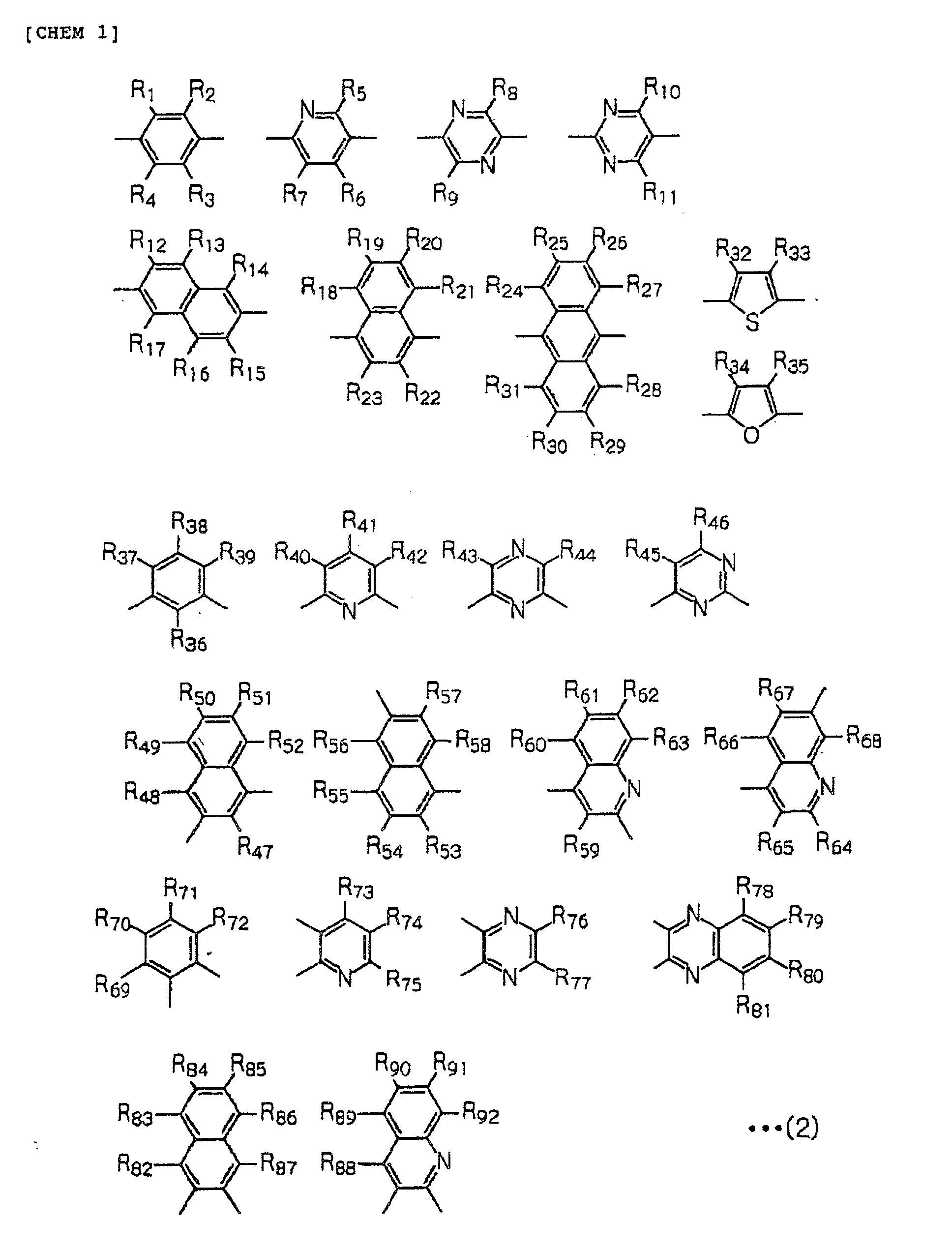
Ar of the macromolecular fluorescent substance expressed by chemical
formula (1) is an arylene or heterocyclic group in which the number of carbons
involved in conjugated bonds is in the range of 4 to 20, and is an aromatic
group or its derivative, heterocyclic group or its derivative, or a group
derived from their combination which are expressed by chemical formulas (2)
shown below.
(R1 to R92 are each a group selected from the group consisting of hydrogen;
alkyl, alkoxy and alkylthio having a carbon number in the range of 1 to 20;
aryl and aryloxy having a carbon number in the range of 6 to 18, and a
heterocyclic group having a carbon number in the range of 4 to 14.)
In these groups, preferred groups are phenylene, substituted phenylene,
biphenylene, substituted biphenylene, naphthalenediyl, substituted
naphthalenediyl, anthracene-9,10-diyl, substituted anthracene-9,10-diyl,
pyridine-2,5-diyl, substituted pyridine-2,5-diyl, thienylene, and
substituted thienylene. More preferred groups are phenylene, biphenylene,
naphthalenediyl, pyridine-2,5-diyl, and thienylene.
When R and R' of chemical formula (1) are substituents other than oxygen
or the cyano group, as for alkyl groups having a carbon number in the range
of 1 to 20, the substituents include methyl, ethyl, propyl, butyl, pentyl,
hexyl, heptyl, octyl, decyl, and lauryl, and preferably methyl, ethyl, pentyl,
hexyl, heptyl, and octyl. As for aryl groups, the substituents include phenyl,
4-alkoxyphenyl having a carbon number in the range of 1 to 12, 4-alkylphenyl
having a carbon number in the range of 1 to 12, 1-naphthyl, and 2-naphthyl.
Preferably, Ar includes at least one group selected from the group
consisting of: alkyl, alkoxy, and alkylthio having a carbon number in the
range of 4 to 20; aryl and aryloxy having a carbon number in the range of
6 to 18; and a heterocyclic group having a carbon number in the range of 4
to 14.
Examples of these substituents are cited below. The alkyl groups having
a carbon number in the range of 4 to 20 include butyl, pentyl, hexyl, heptyl,
octyl, decyl, and lauryl, and preferably pentyl, hexyl, heptyl, and octyl.
The alkoxy groups having a carbon number in the range of 4 to 20 include butoxy,
pentyloxy, hexyloxy, heptyloxy, octyloxy, decyloxy, and lauryloxy, and
preferably pentyloxy, hexyloxy, heptyloxy, and octyloxy. The alkylthio
groups having a carbon number in the range of 4 to 20 include butylthio,
pentylthio, hexylthio, heptylthio, octylthio, decylthio, and laurylthio, and
preferably pentylthio, hexylthio, heptylthio, and octylthio. The aryl groups
include phenyl, 4-alkoxyphenyl having a carbon number in the range of 1 to
12, 4-alkylphenyl having a carbon number in the range of 1 to 12, 1-naphthyl,
and 2-naphthyl. The aryloxy groups include phenoxy. The heterocyclic groups
include 2-thienyl, 2-pyrrolyl, 2-furyl, and 3- and 4-pyridyl. The number
of these substituents is, preferably, at least one relative to a molecular
weight of 600, form the viewpoint of obtaining a highly soluble macromolecular
fluorescent substance, though the number depends the molecular weight of the
macromolecular fluorescent substance and the structure of the repetition
units.
The macromolecular fluorescent substance may be a random, block, or
graft copolymer, or a macromolecule having a structure intermediate between
them, for example, a random copolymer partly having a block copolymer
structure. From the viewpoint of obtaining a macromolecular fluorescent
substance having a high quantum yield, the macromolecular fluorescent
substance is, preferably, a random copolymer partly having a block copolymer
structure, or a block or graft copolymer rather than a fully random copolymer.
Also, the macromolecular fluorescent substance needs to emit light in a solid
state because, in the resulting organic electroluminescent elements,
fluorescence from a thin film is used.
If a solvent is used for the macromolecular fluorescent substance,
preferred solvents include chloroform, methylene chloride, dichloroethane,
tetrahydrofuran, toluene, and xylene. In general, at least 0.1% by weight
of the macromolecular fluorescent substance can be solved in these solvents
though the solubility depends on the structure and molecular weight of the
macromolecular fluorescent substance.
Preferably, the molecular weight of the macromolecular fluorescent
substance is in the range of 103 to 107 when calculated in terms of polystyrene,
and the degree of polymerization depends on the repetition structure and
repetition ratio of the molecule. In general, a preferred total number of
the repetition units is 4 to 10,000, more preferably 5 to 3,000, and still
preferably 10 to 2,000, from the viewpoint of film formability.
The method for synthesizing the macromolecular fluorescent substance
is not particularly limited. However, for example, diphosphonium prepared
from a dialdehyde having an arylene group combined with two aldehyde groups,
a compound having an arylene group combined with two methyl halide groups,
and triphenylphosphine is subjected to the Witting reaction. In another
method, a compound having an arylene group combined with two methyl halide
groups may be subjected to dehydrohalogenation. Also, the macromolecular
fluorescent substance may be prepared by sulfonium salt decomposition in
which an intermediate produced by polymerizing a sulfonium salt having an
arylene group combined with two methyl halide groups with an alkali is
subjected to heat treatment. In any method, by adding a monomer compound
having a skeleton other than arylene groups to vary the monomer content, the
structure of the repetition units contained in the resulting macromolecular
fluorescent substance can be varied. Thus, in order to perform
copolymerization, materials may be prepared so that the content of the
repetition unit expressed by chemical formula (1) becomes 50 mol% or more.
In these methods, the method using the Wittig reaction is preferable, from
the viewpoint of reaction controlling and the yield.
A method for synthesizing an arylene copolymer, which is one of the
above-described macromolecular fluorescent substances, will now be described.
In order to obtain the macromolecular fluorescent substance by the Witting
reaction, first, for example, a bis-(methyl halide) compound, more
specifically, for example, 2,5-dioctyloxy-p-xylylenedibromide is allowed to
react with triphenylphosphine in a solvent, N,N-dimethylformamide, to
synthesize a phosphonium salt. The product and a dialdehyde, more
specifically, terephthalaldehyde, are subjected to condensation using
lithium ethoxide in, for example, ethyl alcohol by the Witting reaction. Thus,
a macromolecular fluorescent substance containing a phenylene-vinylene group
and a 2,5-dioctyloxy-p-phenylenevinylene group is obtained. In this instance,
in order to prepare a copolymer, at least two diphosphonium salts and/or at
least two dialdehydes may be allowed to react.
When the macromolecular fluorescent substance prepared as in the
above-described processes is used as the material of the luminescent elements,
the purity of the substance affects luminous characteristics. It is,
therefore, preferable to purify the substance by separation, such as
reprecipitation or chromatography, after synthesis.
In order to generate full-color images, three materials, each having
one of three colors red, green, and blue are used for forming the luminescent
layer including the above-described macromolecular fluorescent substance.
These materials are discharged onto the respective pixels AR in predetermined
positions, using a patterning apparatus (ink jet apparatus).
The luminescent material may contain a host material and a guest
material.
In such a luminescent material, preferably, a macromolecular organic
compound or a low-molecular-weight substance is used as the host material,
and a fluorescent dye or a phosphorescent substance is used as the guest
material to change the luminous characteristics of the resulting luminescent
layer.
The macromolecular organic compound may be a low-solubility compound
capable of forming a conjugated macromolecular organic electroluminescent
layer through the processes of applying its precursor and subsequently being
subjected to the heat curing reaction expressed by formula (3). For example,
if its precursor is a sulfonium salt, the sulfonium group is removed by heat
treatment to form a conjugated macromolecular organic compound.
Also, the macromolecular organic compound may be a high-solubility
compound capable of forming a luminescent layer through the processes of
applying the compound and removing the solvent.
The above-described macromolecular organic compound is solid and highly
fluorescent, and can be formed into a uniform solid ultrathin film. In
addition, the macromolecular organic compound has excellent formability and
enhanced adhesion to the ITO electrode, and is formed into a hard conjugated
macromolecular film after curing.
For example, poly(arylene-vinylene) is suitable for the macromolecular
organic compound. Poly(arylene-vinylene) is soluble in water-type solvents
and organic solvents and facilitates the preparation of the liquid applied
to the second base material 11. In addition, poly(arylene-vinylene) can be
formed into a high-quality thin film in terms of optics because it can be
polymerized under specific conditions.
Such poly(arylene-vinylenes) include PPV derivatives, such as PPV
(poly(para-phenylene-vinylene), MO-PPV
(poly(2,5-dimethoxy-1,4-phenylene)), CN-PPV
(poly(2,5-bishexyloxy-1,4-phenylene-(1-cyanovinylene))), and MEH-PPV
(poly[2-methoxy-5-(2'-ethylhexyloxy)]-para-phenylene-vinylene);
poly(alkylthiophene), such as PTV (poly(2,5-thienylene-vinylene)); PFV
(poly(2,5-furylene-vinylene)); poly(para-phenylene); and polyalkylfluorene.
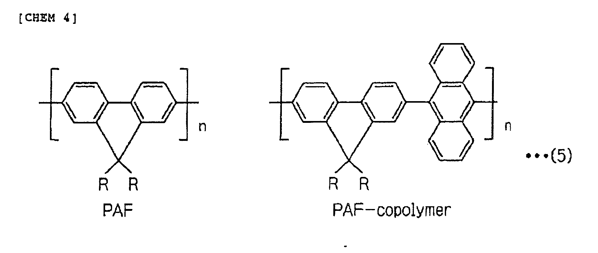
In particular, precursors of PPV and PPV derivatives, expressed by chemical
formula (4), polyalkylfluorene expressed by chemical formula (5)
(specifically, polyalkylfluorene copolymer expressed by chemical formula
(6)) are preferable.
Since PPV and the like are highly fluorescent and are conductive
macromolecules in which π-electrons forming double bonds are delocalized on
the polymer chain, they can form a high-performance organic
electroluminescent element.
Usable macromolecular organic compounds and low-molecular-weight
materials, other than the PPV thin film, used for forming the luminescent
layer, that is, materials used for the host material in the embodiment,
include, for example, generally known materials, such as aluminium quinolinol
complex (Alq3), distyrylbiphenyl, BeBq
2 and Zn(OXZ)
2 expressed by chemical
formula (7), TPD, ALO and DPVBi; and pyrazoline dimers; quinolizine
carboxylic acid; benzopyrylium perchlorate; benzopyranoquinolizine;
rubrene; and phenanthroline europium complex. Using at least one of these
materials, an organic electroluminescent element composition can be
prepared.
Guest materials added to the host material include the above-described
fluorescent dyes and phosphorescent substances. In particular, the
fluorescent dyes can change the luminous characteristics of the luminescent
layer, and can, therefore, increase the luminous efficacy of the luminescent
layer and change the maximum wavelength of light absorption (luminescent
color). Accordingly, the fluorescent dyes can be used as not only a
luminescent layer material but also a color material for functioning to emit
light. For example, the energy of excitons generated by the recombination
of the carriers on conjugated macromolecular organic compound molecules can
be shifted onto fluorescent dye molecules. In this instance, the current
quantum efficiency of the luminescent layer increases because luminescence
is generated from only fluorescent dye molecules having high fluorescence
quantum efficiency. Therefore, by adding the fluorescent dye to the
luminescent layer material, the emission spectrum of the fluorescent
molecules includes that of the luminescent layer. Thus the fluorescent dye
can advantageously serve to change the luminescent color.
The current quantum efficiency here is a yardstick for evaluating
luminescent performance on the basis of luminescent functions, and is defined
by the following equation.
ηE = released photon energy / input electric energy
Also, by doping the luminescent layer with fluorescent dyes to change
the maximum wavelength of light absorption, for example, three primary colors,
red, blue, and green, can be emitted, and consequently, a full color display
can be achieved.
Furthermore, by doping the luminescent layer with fluorescent dyes, the
luminous efficacy of the electroluminescent element can be increased.
When the luminescent layer emits red light, preferably, a laser dye
DCM-1, rhodamine, rhodamine derivatives, phenylene, and the like are used
as a fluorescent dye. By doping the host material, such as PPV, with these
fluorescent dyes, a luminescent layer can be formed. Since many of these
fluorescent dyes are soluble in water, further uniform luminescent layer can
be formed by doping a sulfonium salt, which is a water-soluble PPV precursor,
with such a fluorescent dye and subsequently by heating. Specifically, these
fluorescent dyes include rhodamine B, rhodamine B base, rhodamine 6G, and
rhodamine 101 perchlorate. They may be used in combination.
When the luminescent layer emits green light, preferably, quinacridone,
rubrene, DCJT, and DCJT derivatives are used as a fluorescent dye. As in
the case with the foregoing fluorescent dyes, by doping the host material,
such as PPV, with these fluorescent dyes, the luminescent layer can be formed.
Since many of these fluorescent dyes are soluble in water, further uniform
luminescent layer can be formed by doping a sulfonium salt, which is a
water-soluble PPV precursor, with such a fluorescent dye and subsequently
by heating.
When the luminescent layer emits blue light, preferably,
distyrylbiphenyl and its derivatives are used as a fluorescent dye. As in
the case with the foregoing fluorescent dyes, by doping the host material,
such as PPV, with these fluorescent dyes, the luminescent layer can be formed.
Since many of these fluorescent dyes are soluble in water, further uniform
luminescent layer can be formed by doping a sulfonium salt, which is a
water-soluble PPV precursor, with such a fluorescent dye and subsequently
by heating.
Other fluorescent dyes capable of emitting blue light include coumarin
and its derivatives. These fluorescent dyes have good compatibility with
PPV and, consequently, facilitate the formation of the luminescent layer.
In these dyes, some types of coumarin are insoluble in solvents. By selecting
a suitable substituent, however, the solubility can be increased and they
can become soluble in solvents. Specifically, these fluorescent dyes include
coumarin 1, coumarin 6, coumarin 7, coumarin 120, coumarin 138, coumarin 152,
coumarin 153, coumarin 311, coumarin 314, coumarin 334, coumarin 337, and
coumarin 343.
Other fluorescent dyes capable of emitting blue light include
tetraphenylbutadiene (TPB), TPB derivatives, and DPVBi. As in the case with
the forgoing red fluorescent dyes, these fluorescent dyes are soluble in water
and have good compatibility with PPV, consequently facilitating the formation
of the luminescent layer.
All the fluorescent dyes described above may be used singly or in
combination.
As such fluorescent dyes, the compounds expressed by chemical formulas
(8), (9), and (10) may be used.
Preferably, the fluorescent dye is added, by a method described later,
in an amount of 0.5% to 10% by weight to the host material containing the
above-described conjugated macromolecular organic compound and the like, and
more preferably in an amount of 1.0% to 5.0% by weight. An excessive amount
of the fluorescent dye degrades the weather resistance and durability of the
resulting luminescent layer. In contrast, an excessively small amount of
the fluorescent dye does not lead to sufficient results.
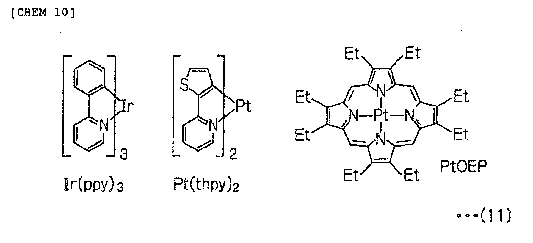
As phosphorescent materials added to serve as a guest material,
preferably, Ir(ppy)
3, Pt(thpy)
2, and PtOEP expressed by chemical formula (11)
and the like are used.
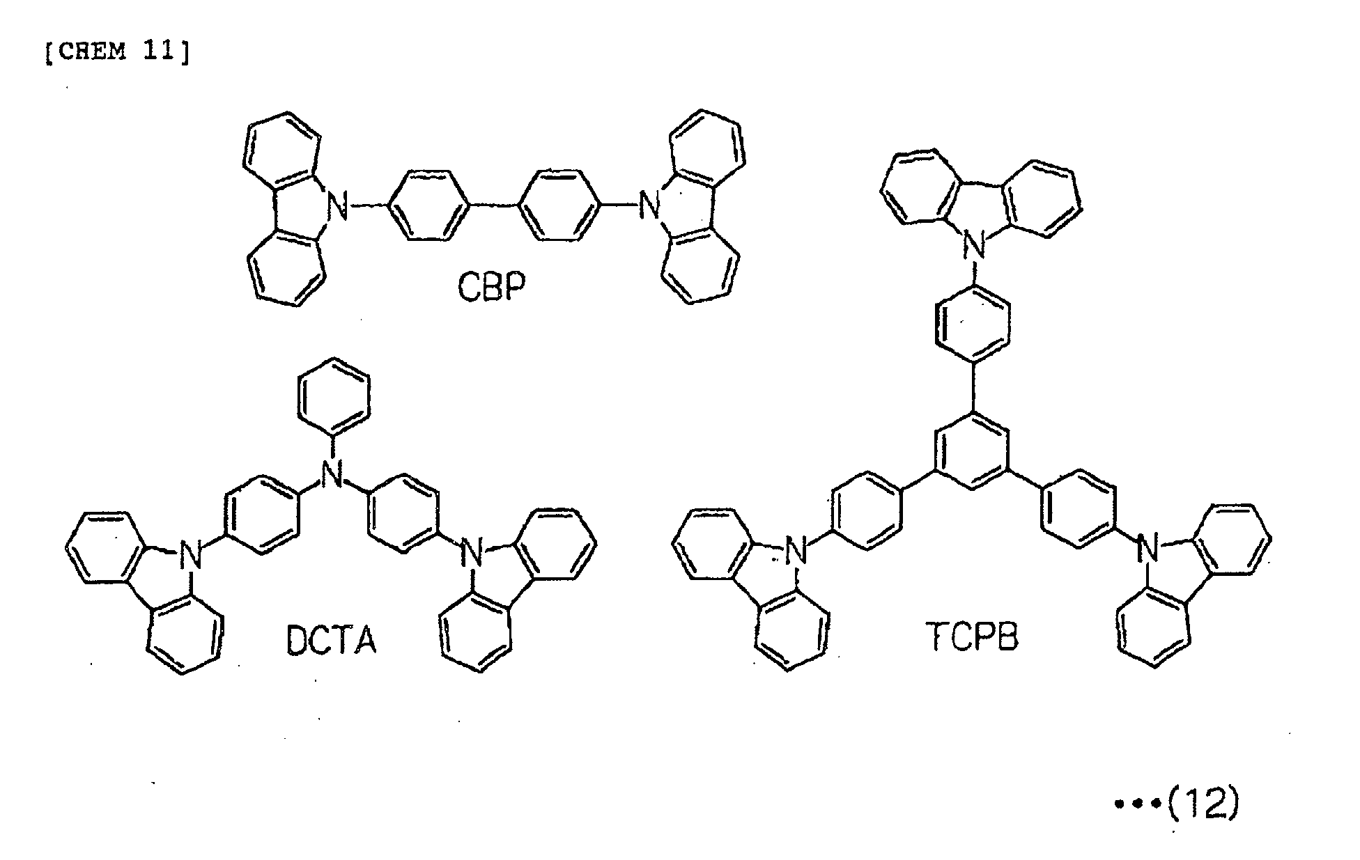
When one of the phosphorescent materials of chemical formula (11) is
used as the guest material, CBP, DCTA, and TCPB which are expressed by chemical
formula (12) and the above-described DPVBi and Alq3 are advantageously used
as the host material.
The above-described fluorescent dyes and phosphorescent materials may
be added together to the host material to serve as guest materials.
When the luminescent layer 60 comprises these host/guest type materials,
a plurality of material supply systems, such as nozzles, are provided to a
patterning apparatus (ink jet apparatus) in advance, and the nozzles
simultaneously discharge the host and guest materials at a predetermined
ratio. Thus, the luminescent layer 60 can be formed which comprises a
luminescent material prepared by adding a desired amount of the guest material
to the host material.
The luminescent layer 60 is formed as in the procedure for forming the
hole injection/transfer layer 70. Specifically, an ink composition
containing luminescent materials are deposited on the surface of the hole
injection/transfer layer 70 by ink jet technique, followed by drying and
heating. Thus, the luminescent layer 60 is formed on the hole
injection/transfer layer 70 in the opening 221a formed in the third insulating
layer 221. This luminescent layer-forming step is also conducted in an
atmosphere of an inert gas. The discharged ink composition is repelled form
the region subjected to ink-repellent treatment. Therefore, even if an ink
drop deviates from a predetermined discharge position, the repelled ink drop
falls into the opening 221a of the third insulating layer 221.
The electron transfer layer 50 is formed on the upper surface of the
luminescent layer 60. The electron transfer layer 50 is also formed by an
ink jet technique, as in the luminescent layer 60. The material of the
electron transfer layer 50 is not particularly limited. Exemplary electron
transfer layer materials include oxadiazole derivatives,
anthraquinodimethane and its derivatives, benzoquinone and its derivatives,
naphthoquinone and its derivatives, anthraquinone and its derivatives,
tetracyanoanthraquinodimethane and its derivatives, fluorenone derivatives,
diphenyldicyanoethylene and its derivatives, diphenoquinone derivatives,
and 8-hydroxyquinoline and metal complexes of its derivatives. Specifically,
materials disclosed in Japanese Unexamined Patent Application Publication
Nos. 63-70257, 63-175860, 2-135359, 2-135361, 2-209988, 3-37992, and
3-152184, preferably triphenyldiamine derivatives are used, as in the
above-described hole transfer layer. In particular,
2-(4-biphenylyl)-5-(4-t-butylphenyl)-1,3,4-oxadiazole, benzoquinone,
anthraquinone, and tris(8-quinolinol)aluminum are preferable.
The materials of the hole injection/transfer layer 70 and the electron
transfer layer 50 may be mixed with the material of the luminescent layer
60 to be used as a luminescent layer material. In this instance, the contents
of the hole injection/transfer material and the electron transfer material
are appropriately determined so as not to suppress the film formability and
luminous characteristics though the contents depend on the types of the
compounds used. They are generally in the range of 1% to 40% by weight relative
to the luminescent material, and preferably in the range of 2% to 30% by
weight.
The hole injection/transfer layer 70 and the electron transfer layer
50 are not limited to being formed by an ink jet technique, but may be formed
by mask deposition.
The cathode 222 may cover the entire surfaces of the electron transfer
layer 50 and the third insulating layer 221, or may be disposed in a striped
manner. The cathode 222 may be formed in a single layer of an elementary
substance, such as Al, Mg, Li, and Ca, or an alloy of Mg:Ag (10:1), or in
two or three metal (including alloy) layers. Specifically, a laminate, such
as Li2O (about 0.5 nm)/Al, LiF (about 0.5 nm)/Al, or MgF2/Al, may be used.
The cathode 222 is a light-transmissive metal thin film.
The sealing layer 20 is intended to prevent air from entering the organic
EL elements from the outside, and the thickness and the material are
appropriately selected. As the material of the sealing layer 20, for example,
ceramic, silicon nitride, silicon nitride oxide, or silicon oxide is used.
In particular, silicon nitride oxide is preferable from the viewpoint of
transparency and gas interruption. The sealing layer 20 may be formed on
the cathode 222 by plasma CVD.
As described above, light emitted from the luminescent layer 60 passes
through the insulating layers 283 and 284 formed of a material having a
refractive index lower than that of the member 2 and enters the member 2.
Light entering the insulating layers 283 and 284 at an angle more than or
equal to the critical angle is refracted in a direction forming an angle less
than or equal to the critical angle at the interface with the member 2, and
is thus deviated from total reflection conditions to be emitted to the outside.
Thus, light emission efficiency can be increased to achieve an enhanced
visibility. There is a strong correlation between the refractive index and
the dielectric constant. The low-refractive- index insulating layers 283 and
284 have low dielectric constants, and consequently, the capacity between
wires can be reduced. Thus, the operation performance of electro-optical
devices, such as operation speed, can be enhanced.
In addition to the hole injection/
transfer layer 70, the
luminescent
layer 60, and the
electron transfer layer 50, a hole blocking layer may be
provided on the opposing
electrode 222 side of the
luminescent layer 60 to
increase the lifetime of the
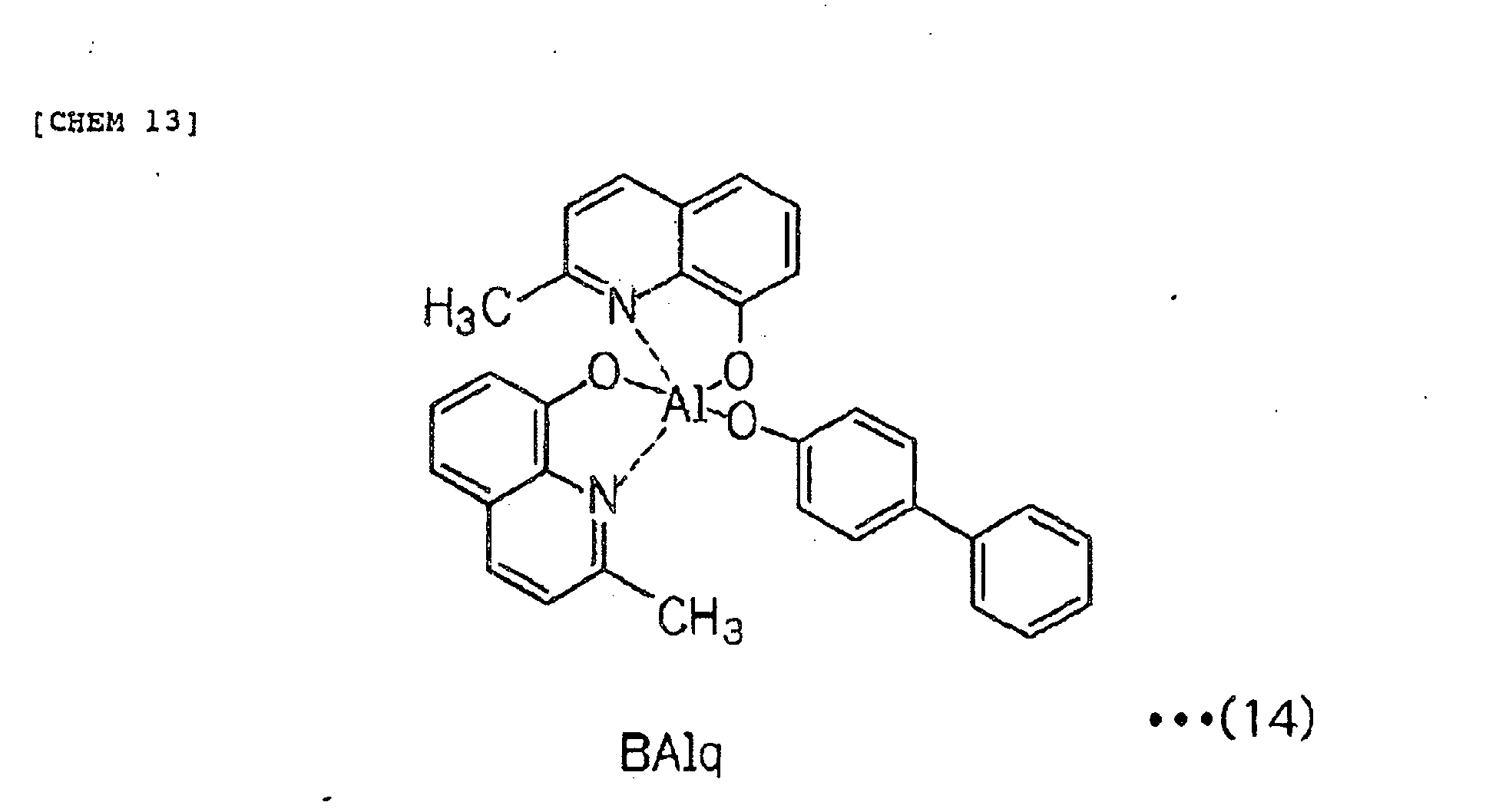
luminescent layer 60. The constituent of the
hole blocking layer may be BCP expressed by chemical formula (13) or BAlq
expressed by chemical formula (14), and preferably BAlq is used, from the
viewpoint of the increase of lifetime.
An electronic apparatus including an organic EL display device
according to the above-described embodiment will now be describe.
Fig. 4 is a perspective view of a cellular phone. In Fig. 4, reference
numerals 1000 and 1001 represent a body of the cellular phone and a display
using the above-described organic EL display device, respectively.
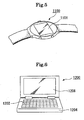
Fig. 5 is a perspective view of a wrist watch type electronic apparatus.
In Fig. 5, reference numerals 1100 and 1101 represent a body of the wrist
watch and a display using the above-described organic EL display device,
respectively.
Fig. 6 is a perspective view of a portable information processing
apparatus such as a word processor or a personal computer. In Fig. 6 reference
numerals 1200, 1202, 1204, and 1206 represent an information processing
apparatus, an input region such as a keyboard, a body of the information
processing apparatus, and a display including the above-described organic
EL display device, respectively.
Since the electronic apparatuses shown in Figs. 4 to 6 each include the
organic EL display device according to the above-described embodiment,
high-quality, bright images can be achieved.
The technical scope of the present invention is not limited to the
embodiments illustrated above, but various modifications may be made without
departing from the purpose of the invention.
For example, in the embodiment, the organic EL element includes the
luminescent layer and the hole transfer layer which are held between a pair
of electrodes; however, the organic EL element may include organic layers
having various functions, such as an electron transfer layer, a hole injection
layer, and an electron injection layer, in addition to the luminescent layer
and the hole transfer layer. Also, the materials cited in the embodiment
are no more than examples and can be changed, if necessary.
In the display device S1 of the embodiment, the luminescent layer 60
acting as an electro-optical element may be replaced with a liquid crystal
layer or other optical display materials.
In the embodiment, a back emission type display device in which light
is emitted from the member 2 side having the TFTs 24 is described. However,
the low-refractive-index layer of the present invention can be used in a
so-called top emission type display device in which light is emitted from
the other side opposite the member having the TFTs.
According to the present invention, light emitted from electro-optical
elements passes through low-refractive-index material layers having a
refractive index lower than that of the member and enters the member. Light
entering the low-refractive-index layers at an angle more than or equal to
the critical angle is refracted in a direction forming an angle less than
or equal to the critical angle at the interface with the member, and is thus
deviated from total reflection conditions to be emitted to the outside. Thus,
light emitting efficiency can be increased to achieve an enhanced visibility.
Also, there is a strong correlation between the refractive index and the
dielectric constant. By forming predetermined material layers having a low
refractive index, the resulting low-refractive-index layers have a low
dielectric constant, and consequently, the capacity between wires can be
reduced. Thus, the operation performance of electro-optical devices, such
as operation speed, can be enhanced.