EP1321850A2 - Mikroprozessor mit Rechnungseinheit - Google Patents
Mikroprozessor mit Rechnungseinheit Download PDFInfo
- Publication number
- EP1321850A2 EP1321850A2 EP02258677A EP02258677A EP1321850A2 EP 1321850 A2 EP1321850 A2 EP 1321850A2 EP 02258677 A EP02258677 A EP 02258677A EP 02258677 A EP02258677 A EP 02258677A EP 1321850 A2 EP1321850 A2 EP 1321850A2
- Authority
- EP
- European Patent Office
- Prior art keywords
- calculation
- partial
- data
- bit width
- mode
- Prior art date
- Legal status (The legal status is an assumption and is not a legal conclusion. Google has not performed a legal analysis and makes no representation as to the accuracy of the status listed.)
- Withdrawn
Links
Images
Classifications
-
- G—PHYSICS
- G06—COMPUTING; CALCULATING OR COUNTING
- G06F—ELECTRIC DIGITAL DATA PROCESSING
- G06F9/00—Arrangements for program control, e.g. control units
- G06F9/06—Arrangements for program control, e.g. control units using stored programs, i.e. using an internal store of processing equipment to receive or retain programs
- G06F9/30—Arrangements for executing machine instructions, e.g. instruction decode
- G06F9/30003—Arrangements for executing specific machine instructions
- G06F9/30007—Arrangements for executing specific machine instructions to perform operations on data operands
- G06F9/3001—Arithmetic instructions
- G06F9/30014—Arithmetic instructions with variable precision
-
- G—PHYSICS
- G06—COMPUTING; CALCULATING OR COUNTING
- G06F—ELECTRIC DIGITAL DATA PROCESSING
- G06F7/00—Methods or arrangements for processing data by operating upon the order or content of the data handled
- G06F7/38—Methods or arrangements for performing computations using exclusively denominational number representation, e.g. using binary, ternary, decimal representation
- G06F7/48—Methods or arrangements for performing computations using exclusively denominational number representation, e.g. using binary, ternary, decimal representation using non-contact-making devices, e.g. tube, solid state device; using unspecified devices
- G06F7/57—Arithmetic logic units [ALU], i.e. arrangements or devices for performing two or more of the operations covered by groups G06F7/483 – G06F7/556 or for performing logical operations
Definitions
- the present invention relates to microprocessors, particularly, a technique to reduce electric power consumption of microprocessors.
- a processor such as a VLIW (Very Long Instruction Word) microprocessor that includes a plurality of independent processing elements
- VLIW Very Long Instruction Word
- a technique for controlling parallelism of a plurality of CPUs according to their system operation environment settings is disclosed in US Patent 5,913,068.
- Microprocessors installed in such multi-functional information processing machines are required to execute various kinds of application programs involving different types of data such as an application program focusing on control of graphical user interface or audio-visual digital signal processing, for example.
- each of such application programs includes calculation instructions specifying data calculation e.g. an addition, although types of data being treated are different from one application program to another.
- all the calculation instructions in different application programs are processed in the same data calculation circuit in a microprocessor.
- an object of the present invention is to provide a microprocessor with a mechanism that is capable of reducing electric power consumption in execution of data calculation, while maintaining the level of calculation performance required for different types of data that are treated in different application programs to be executed by the microprocessor.
- Another object of the present invention is to provide a microprocessor that is capable of increasing the speed of data calculation when application programs to be executed treat a certain type of data that satisfies a condition. Since microprocessors are required to be all-purpose and to work on various kinds of data, such capability is beyond a basic performance level of microprocessors.
- the present invention provides a microprocessor that performs processing according to an instruction fetched from a memory, comprising: a calculation circuit that (i) includes partial calculation circuits which each perform partial data calculation, and (ii) is operable to perform data calculation on N or less bits, where N is a total number of bits on which the partial calculation circuits are to perform data calculation; a bit width selecting unit operable to select a bit width mode that designates a certain number of bits on which data calculation is to be performed; an execution controlling unit operable to, if the fetched instruction is an instruction for data calculation, control the calculation circuit to perform data calculation; and an operation controlling unit operable to, when the execution controlling unit controls the calculation circuit to perform data calculation, (i) have all the partial calculation circuits operate, in a case where the bit width selecting unit selects a first bit width mode designating
- the second bit width mode it is possible to make electric power consumption less than in the case where the first bit width mode is selected, since only a certain number of partial calculation circuits operate.
- a bit width mode depending on the level of calculation performance required by each of the application programs, in other words, depending on an effective number of bits for data calculation required by each of the application programs, it is possible to reduce electric power consumption on account of unused partial calculation circuits, if any, because the operation controlling unit has only required partial calculation circuits operate among the partial calculation circuits included in a function block that performs calculation.
- the microprocessor may have an arrangement, wherein the partial calculation circuits each perform partial data calculation upon receiving a clock signal, and the operation controlling unit (i) in a case where the bit width selecting unit selects the first bit width mode, supplies a clock signal to each of all the partial calculation circuits, and (ii) in a case where the bit width selecting unit selects the second bit width mode, suspends the supply of a clock signal to a predetermined number of the partial calculation circuits, and supplies a clock signal to each of the rest of the partial calculation circuits.
- the microprocessor may have an arrangement, wherein the partial calculation circuits each include a calculator and a bit data obtaining circuit, the calculator performing data calculation on a number of bits of data supplied, and the bit data obtaining circuit, upon receiving a clock signal, obtaining the number of bits of data from one or more data buses and supply to the calculator, the number being specific to each of the partial calculation circuits, and the operation controlling unit supplies a clock signal to each of the partial circulation circuits by supplying a clock signal to each of the bit data obtaining circuits.
- the microprocessor may have an arrangement, wherein the partial calculation circuits, except for a partial calculation circuit that performs data calculation on a most significant bit of the N bits, are each operable to output a carry bit signal indicating an overflow occurring during data calculation, the calculation circuit includes a carry bit signal transmitting unit that inputs to each of all the partial calculation circuits except for a partial calculation circuit that performs data calculation on a least significant bit of the N bits, a carry bit signal outputted from a partial calculation circuit that performs data calculation on a number of less significant bits than the particular partial calculation circuit to which such a carry bit signal is to be inputted does, and the microprocessor further comprises a carry bit signal inhibiting unit operable to, in a case where the bit width selecting unit selects the second bit width mode, inhibit the carry bit signal transmitting unit from inputting a carry bit signal to the predetermined number of the partial calculation circuits to which the supply of a clock signal is suspended by the operation controlling unit.
- the partial calculation circuits except for a partial calculation circuit that performs data
- the microprocessor has capability of easily increasing the speed of processing and reducing the electric power consumption, because it is possible to partially inhibit the transmission of carry bit signals in the case where the second bit width mode is selected. Consequently, such capability is useful in realizing a microprocessor that is power-saving and has a high performance level. For instance, by providing another controlling unit operable to control the level of the voltage to be impressed on each of the calculators, it would be possible to lower a little the level of the voltage to be impressed on the entire calculation circuit without lowering the speed of the calculation, as long as the second bit width mode is selected. By providing another controlling unit operable to control the frequency of the clock signals to be supplied to each of the calculators, it would be possible to increase the speed of calculation a little, as long as the second bit width mode is selected.
- the microprocessor may further comprise a clock frequency controlling unit operable to (i) control the operation controlling unit to supply the clock signal of a first frequency to each of the partial calculation circuits, in a case where the bit width selecting unit selects the first bit width mode, and (ii) control the operation controlling unit to supply the clock signal of a second frequency, which is higher than the first frequency, to each of the partial calculation circuits, in a case where the bit width selecting unit selects the second bit width mode.
- a clock frequency controlling unit operable to (i) control the operation controlling unit to supply the clock signal of a first frequency to each of the partial calculation circuits, in a case where the bit width selecting unit selects the first bit width mode, and (ii) control the operation controlling unit to supply the clock signal of a second frequency, which is higher than the first frequency, to each of the partial calculation circuits, in a case where the bit width selecting unit selects the second bit width mode.
- the microprocessor may further comprise a voltage controlling unit operable to control a voltage level so as to (i) impress a voltage of a first voltage level on the calculation circuit in a case where the bit width selecting unit selects the first bit width mode, and (ii) impress a voltage of a second voltage level, which is lower than the first voltage level, on the calculation circuit in a case where the bit width selecting unit selects the second bit width mode.
- a voltage controlling unit operable to control a voltage level so as to (i) impress a voltage of a first voltage level on the calculation circuit in a case where the bit width selecting unit selects the first bit width mode, and (ii) impress a voltage of a second voltage level, which is lower than the first voltage level, on the calculation circuit in a case where the bit width selecting unit selects the second bit width mode.
- the microprocessor may further comprise a clock frequency controlling unit operable to (i) control the operation controlling unit to supply the clock signal of a first frequency to each of the partial calculation circuits, in a case where the bit width selecting unit selects the first bit width mode, and (ii) control the operation controlling unit to supply the clock signal of a second frequency, which is higher than the first frequency, to each of the partial calculation circuits, in a case where the bit width selecting unit selects the second bit width mode; a voltage controlling unit operable to control a voltage level so as to (i) impress a voltage of a first voltage level on the calculation circuit in a case where the bit width selecting unit selects the first bit width mode, and (ii) impress a voltage of a second voltage level, which is lower than the first voltage level, on the calculation circuit in a case where the bit width selecting unit selects the second bit width mode; a control mode selecting unit operable to select a control mode in terms of the frequency of the clock signal to be supplied "to each of the partial calculation circuits, and the voltage
- the microprocessor is able to choose either increasing the speed of data calculation or reducing the electric power consumption for data calculation, and, for example, is able to specify such a choice for each application program and the like.
- the microprocessor may further comprise a signal stabilizing unit operable to maintain at a predetermined level, for a predetermined period of time, a voltage level of a signal line used for outputting a signal to outside of the microprocessor, the predetermined period starting from when the control mode selecting unit changes from one control mode to another control mode.
- a signal stabilizing unit operable to maintain at a predetermined level, for a predetermined period of time, a voltage level of a signal line used for outputting a signal to outside of the microprocessor, the predetermined period starting from when the control mode selecting unit changes from one control mode to another control mode.
- the microprocessor may comprise a memory access unit operable to access an external memory, wherein if the fetched instruction is an instruction for data-writing into a memory, the execution controlling unit has the memory access unit write one or more pieces of data into the external memory, and the bit width selecting unit selects a bit width mode according to a value stored in a predetermined area of the external memory.
- each application program is able to easily inform the microprocessor of such information required for judging conditions of suspending operation of a certain number of partial calculation circuits, i.e. a value of a bit width, by setting a bit width mode in a predetermined memory area, the bit width mode determined based on an effective number of bits in data calculation.
- a bit width mode determined based on an effective number of bits in data calculation.
- the microprocessor may have an arrangement, wherein if the fetched instruction is an instruction for data calculation, the bit width selecting unit selects (i) the first bit width mode, in a case where the fetched instruction is an instruction for data calculation on N bits, and (ii) the second bit width mode, in a case where the fetched instruction is an instruction for data calculation on less than N bits.
- the microprocessor is able to execute with less electric power consumption an application program that is constructed only with instructions for data calculation on 8-bit data, than in the case where an application program is constructed only with instructions for data calculation on 16-bit data.
- an application program or a program routine that processes moving image compression or decompression in low image quality and (b) an application program or a program routine that processes moving image decompression in high image quality
- the number of bits required for calculation is different; therefore, it would be possible to reduce electric power consumption in execution of the former application program than in execution of the latter, by constructing each of the application programs with calculation instructions with the specific number of bits required.
- the microprocessor may comprise: a data storage unit including an area that stores therein a result of data calculation performed by the calculation circuit, the result being N bits; and a data writing controlling unit operable to (i) in a case where the first bit width mode is selected, have the entire N bits of the result written in the area and (ii) in a case where the second bit width mode is selected, have only a part of the result being less than N bits written in the area.
- the microprocessor may comprise a data writing controlling unit operable to (i) in a case where the first bit width mode is selected, have the entire N bits of a result outputted from the calculation circuit written in an external memory, and (ii) in a case where the second bit width mode is selected, have only a part of the result being less than N bits written in the external memory.
- the microprocessor may have an arrangement, wherein the calculation circuit includes two partial calculation circuits that each perform partial data calculation on N/2 bits, and the execution controlling unit, if the fetched instruction is an instruction for data calculation on N bits, and also in a case where the bit width selecting unit selects the second bit width mode, (i) have one of the partial calculation circuits perform partial data calculation on lower N/2 bits out of the N bits, before (ii) having the same partial calculation circuit perform partial data calculation on upper N/2 bits, while taking account of an overflow, if any, that has occurred during the partial data calculation on the lower N/2 bits.
- the microprocessor may have an arrangement, wherein the partial calculation circuits each perform partial data calculation upon receiving a number of bits of data supplied, and the operation controlling unit (i) supplies to each of all the partial calculation circuits as many number of bits of as possible for that particular partial calculation circuit, in a case where the bit width mode selecting unit selects the first bit width mode, and (ii) suspends the supply of bits of data to a predetermined number of the partial calculation circuits, and supplies to each of the rest of the partial calculation circuits, as many number of bits as possible for that particular partial calculation circuit, in a case where the bit width mode selecting unit selects the second bit width mode.
- the microprocessor may have an arrangement, wherein each of the partial calculation circuits performs data calculation while a predetermined level of a voltage is being impressed thereon, and the operation controlling unit (i) impresses the predetermined level of the voltage on each of all the partial calculation circuits, in a case where the bit width selecting unit selects the first bit width mode, and (ii) suspends the impression of the predetermined level of the voltage on a predetermined number of the partial calculation circuits, and impresses the predetermined level of the voltage on each of the rest of the partial calculation circuits, in a case where the bit width selecting unit selects the second bit width mode.
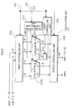
- FIG. 1 is a functional block diagram of the processor 100 in the first embodiment of the present invention.
- the processor 100 is a processor that decodes instructions in a program stored in an external memory and executes processing specified by those instructions.
- the processor 100 is constructed with a CMOS (Complementary Metal Oxide Semiconductor) and includes the instruction memory 110, the instruction decode unit 120, the instruction execute unit 130, the data memory 140, the voltage controlling unit 150, the frequency controlling unit 160, and the bus width controlling unit 170, as shown in the functional block diagram in FIG. 1.
- CMOS Complementary Metal Oxide Semiconductor
- the instruction memory 110 is a cache memory for storing instructions to be executed that are fetched from an external memory.
- the external memory stores programs such as various kinds of application programs for specific purposes and an operating system to control the execution of those application programs. All the instructions necessary for the execution of those programs are fetched by the instruction memory 110.
- the effective value of numerical data treated in application programs may vary from one application program to another, for example, it could be less than a hundred, less than two thousand, or less than thirty thousand. It means that some application programs treat only such data that can be expressed with 8 bits, and some with 12 bits, and some with 16 bits. In addition, some application programs need to be executed at high speed, and some applications do not need to be executed at high speed but the electric power consumption therefore should be reduced. It is understood that programmers and system designers are able to recognize in advance such characteristics of each application program, and it is assumed that application programs are structured so that a bus width mode and an operation mode (to be explained later) can be specified within each program.
- the instruction decode unit 120 is a circuit that fetches an instruction from the instruction memory 110 and decodes it one by one, and transmits, according to the results of the decoding, a control signal to a specific circuit etc. in the instruction execute unit 130 so as to have the specific circuit operate.
- the instruction decode unit 120 also instructs the voltage controlling unit 150, the frequency controlling unit 160, and the bus width controlling unit 170 to change their controlling actions when a specific instruction has been decoded.
- An example of such specific instructions is a dedicated instruction indicating that the application program to be executed has been changed (hereafter referred to as a CHANGE instruction), which is to be specified within an application program.
- the instruction decode unit 120 transmits the above-mentioned control signal according to the results of the decoding of instructions; therefore, for example, in the case where the instruction decode unit 120 has decoded an add instruction, the instruction decode unit 120 transmits a control signal to control a switching element provided in the signal line for supplying clock signals so that the clock signals (CLK) from the frequency controlling unit 160 would be supplied to the clock gating controlling unit 136 in the calculation unit 131.
- CLK clock signals
- the instruction execute unit 130 is made up of various circuits such as the calculation unit 131, the transfer unit 139, and so on.
- calculation unit 131 is a typical example of circuits that perform data calculation of 16-bit data, and it is assumed that the calculation unit 131 here is an adding circuit that adds up two pieces of 16-bit data that are inputted and outputs a piece of 16-bit data as a result.
- the transfer unit 139 is a circuit that transfers the data in an external memory to the data memory 140 in the processor.
- the instruction execute unit 130 includes various data calculation circuits such as arithmetic circuits including a multiplying circuit etc. and logic circuits, as well as a circuit for transferring some data in the data memory 140 to an external memory.
- the data memory 140 is a cache memory and register that stores data, and includes the bus width mode area 148 for storing bus width modes, and the operation mode area 149 for storing operation modes.
- the data memory 140 is connected via buses with various circuits such as calculation unit 131 in the instruction execute unit 130.
- the bus width modes are modes to specify the number of bits required for data calculation, either the 16-bit mode, the 12-bit mode, or the 8-bit mode.
- the operation modes are modes to specify control related to electric-power-saving and higher speeds, namely, the normal mode, the high-speed mode, or the low electric power consumption mode.
- Each application program is arranged to include, before a CHANGE instruction mentioned above, a data transfer instruction for transferring such data in the external memory that indicates the bus width mode and the operation mode to either the bus width mode area 148 or operation mode area 149 in the data memory. If the instruction decode unit 120 decodes a data transfer instruction and has the transfer unit 139 execute the transfer, then as a result, the bus width mode area 148 stores a bus width mode specified by the application program and the operation mode area 149 stores a operation mode specified by the application program.
- the voltage controlling unit 150 controls the voltages to be impressed on functional blocks in the processor. It sometimes performs controlling so that no voltage is impressed on an unused functional block, and sometimes so that a voltage level to be impressed on the calculation unit 131 would be changed according to the bus width mode and the operation mode, with a trigger of the instruction decode unit 120 instructing the voltage control unit 150 to change its controlling actions.
- the frequency controlling unit 160 supplies clock signals to each functional block in the processor, and controls the frequencies of clock signals and the like. It sometimes performs controlling so that no clock signals are supplied to an unused functional block, and sometimes so that the frequency of clock signals to be supplied to the calculation unit 131 would be changed according to the bus width mode and the operation mode, with a trigger of the instruction decode unit 120 instructing the frequency controlling unit 160 to change its controlling actions .
- the processor 100 includes a mechanism which performs controlling so that the voltage level of a certain terminal that connects the processor 100 with an external circuit should be maintained, for a predetermined time e.g. some ten milliseconds, at the same level as a low-level standard voltage of the substrate on which the processor 100 is installed, for instance, in the event that (i) the voltage controlling unit 150 performs controlling so that no voltage is impressed on an unused functional block and some voltage is impressed on functional blocks in use, or so that the voltage levels should be changed, and (ii) the frequency controlling unit 160 performs controlling so that the clock frequency should be changed.
- the voltage controlling unit 150 and the frequency controlling unit 160 each transmit to the controlling mechanism such a signal that indicates a control action of changing the state of voltage or frequency is to be performed.
- the controlling mechanism such as a signal that indicates a control action of changing the state of voltage or frequency is to be performed.
- bus width controlling unit 170 refers to the bus width mode area 148 with a trigger of the instruction decode unit 120 instructing the bus width controlling unit 170 to change its controlling actions, and, for example, performs controlling by expressing each of the bus width modes with an identifiable 2-bit signal and informing the calculation unit 131 of a selected bus width mode.
- FIG. 2 shows a detailed structure of the calculation unit 131 of the first embodiment.
- the calculation unit 131 is a circuit that performs calculation on two pieces of 16-bit data that are indicated as "srcA” and “srcB” in the drawing, and outputs carry bit signals (carry) to indicate whether a carry has occurred or not, as well as pieces of 16-bit data indicated as “dest” in the drawing, as results of the calculation.
- the calculation unit 131 includes the partial calculation units 132a, 132b, and 132c, the carry transmitting units 134a and 134b, the carry selecting circuit 135, the clock gating controlling unit 136 and the carry controlling unit 137.
- the partial calculation unit 132a performs calculation on a piece of 8-bit data starting with the least significant bit of the 16-bit data inputted for calculation, and outputs a piece of 8-bit data and a carry bit signal as results of the calculation.
- the partial calculation unit 132a includes (i) a section that reads a piece of 8-bit data to be calculated upon a clock signal being supplied, (ii) a calculator 133a that adds up two pieces of 8-bit data upon the reading, and (iii) a section that outputs a piece of 8-bit data and a carry bit signal as results of the calculation upon a clock signal being supplied.
- the partial calculation unit 132b performs calculation on a piece of 4-bit data starting with the 8 th bit of the 16-bit data inputted for calculation (with the least significant bit counted as a 0 th bit), and outputs a piece of 4-bit data and a carry bit signal as results of the calculation.
- the partial calculation unit 132b includes (i) a section that reads a piece of 4-bit data to be calculated upon a clock signal being supplied, (ii) a calculator 133b that adds up two pieces of 4-bit data upon the reading, and (iii) a section that outputs a piece of 4-bit data and a carry bit signal as results of the calculation upon a clock signal being supplied.
- the partial calculation unit 132c performs calculation on a piece of 4-bit data ending with the most significant bit of the 16-bit data inputted for calculation, and outputs a piece of 4-bit data and a carry bit signal as results of the calculation .
- the partial calculation unit 132c includes (i) a section that reads a piece of 4-bit data to be calculated upon a clock signal being supplied, (ii) a calculator 133c that adds up two pieces of 4-bit data upon the reading, and (iii) a section that outputs a piece of 4-bit data and a carry bit signal as results of the calculation upon a clock signal being supplied.
- two pieces of 16-bit data are selected that are specified by certain addresses or register IDs in the data memory 140, according to an operand for an addition instruction and the like.
- the two pieces of 16-bit data selected will be placed on each of 16-bit buses and inputted to the calculation unit 131 as srcA [15:0] and srcB [15:0] respectively.
- a piece of 16-bit data, namely dest [15:0] outputted by the calculation unit 131 will be stored in an area specified by a certain address or a register ID in the data memory 140 according to an operand for an addition instruction and the like.
- a carry bit signal (carry) outputted by the calculation unit 131 will be stored in what is called a flag register or the like.
- the carry transmitting unit 134a is a circuit that inputs, under the control of the carry controlling unit 137, a carry bit signal outputted by the calculator 133a to what is called a carry-in terminal of the calculator 133b.
- the carry transmitting unit 134b is a circuit that inputs, under the control of the carry controlling unit 137, a carry bit signal outputted by the calculator 133b to what is called a carry-in terminal of the calculator 133c.
- the carry selecting circuit 135 is a circuit that, under the control of the carry controlling unit 137, selects one of the carry bit signals outputted by the partial calculation units 132a, 132b, and 132c, and outputs the selected carry bit signal as an output signal from the calculation unit 131.
- the clock gating controlling unit 136 receives a signal 183 indicating a bus width mode from the bus width controlling unit 170, and performs controlling by switching individually, for each of the partial calculation units, whether the clock signal 182 supplied by the frequency controlling unit 160 should be transmitted to each of partial calculation units or should be cut off, depending on the bus width mode indicated.
- FIG. 3 is a truth table for inputs to and outputs from the clock gating controlling unit 136.
- a clock signal (CLK) and a bus width mode shown in FIG. 3 are inputted signals; whereas an output signal from the clock gating controlling unit 136 to each of the partial calculation units is determined by a combination of a clock signal (CLK) and a value for a bus width mode.
- the clock gating controlling unit 136 transmits a clock signal to (i) all of the partial calculation units 132a, 132b, and 132c in the case where the bus width mode is the 16-bit mode, (ii) only two of the partial calculation units except for the partial calculation unit 132c in the case where the bus width mode is the 12-bit mode, and (iii) only the partial calculation unit 132a in the case where the bus width mode is the 8-bit mode.
- the carry controlling unit 137 is a circuit that receives a signal 183 indicating a bus width mode from the bus width controlling unit 170, and controls the carry transmitting units 134a, 134b and the carry selecting circuit 135, depending on the bus width mode indicated.
- FIG. 4 is a control table to show control signals outputted by the carry controlling unit 137 based on inputted signals.
- the bus width modes are inputted signals;
- the "carry input to the calculator 133b" is, for example, a 1-bit control signal instructing the carry transmitting unit 134a whether or not the inputted signal should be reflected on the output signal;
- the “carry input to the calculator 133c” is, for example, a 1-bit control signal instructing the carry transmitting unit 134b whether or not the inputted signal should be reflected on the output signal;
- Selection of a carry to be outputted denotes, for example, a 2-bit control signal instructing the carry selecting circuit 135 which calculator should be a source of a carry bit signal that is selected as an output signal from the calculation unit 131.
- the clock gating controlling unit 136 (i) instructs each of the carry transmitting units 134a and 134b to set the output value as the one to reflect the inputted carry bit signal, and also (ii) instructs the carry selecting circuit 135 to select the carry bit signal (carry [2]) inputted by the calculator 133c.
- the clock gating controlling unit 136 (i) instructs the carry transmitting unit 134a to set the output value as the one to reflect the inputted carry bit signal, (ii) instructs the carry transmitting unit 134b not to change the output value, and also (iii) instructs the carry selecting circuit 135 to select the carry bit signal (carry [1]) inputted by the calculator 133b.
- the clock gating controlling unit 136 (i) instructs both of the carry transmitting units 134a and 134b not to change the output values, and also (ii) instructs the carry selecting circuit 135 to select the carry bit signal (carry [0]) inputted by the calculator 133c.
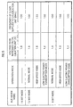
- FIG. 5 is a control table to show the control by the voltage controlling unit 150 and the frequency controlling unit 160 according to different bus width modes and operation modes.
- the voltage controlling unit 150 determines the voltage level to be impressed on the calculation unit 131
- the frequency controlling unit 160 determines the frequency of the clock signals to be supplied to the calculation unit 131.
- the voltage controlling unit 150 impresses a voltage of 1.8 V (volts) on the calculation unit 131, and the frequency controlling unit 160 supplies clock signals of 100 MHz (megahertz) to the calculation unit 131.
- the 12-bit mode is combined with the high-speed mode, then the voltage controlling unit 150 impresses a voltage of 1.8 V on the calculation unit 131, and the frequency controlling unit 160 supplies clock signals of 133 MHz to the calculation unit 131.
- the voltage controlling unit 150 impresses a voltage of 1.6 V on the calculation unit 131, and the frequency controlling unit 160 supplies clock signals of 100 MHz to the calculation unit 131. If the 8-bit mode is combined with the high-speed mode, then the voltage controlling unit 150 impresses a voltage of 1.8 V on the calculation unit 131, and the frequency controlling unit 160 supplies clock signals of 166 MHz to the calculation unit 131. If the 8-bit mode is combined with the low electric power consumption mode, then the voltage controlling unit 150 impresses a voltage of 1. 4 V on the calculation unit 131, and the frequency controlling unit 160 supplies clock signals of 100 MHz to the calculation unit 131.
- calculation at the calculation unit 131 requires transmission of carries, and since the calculation of the upper column should reflect the result of the calculation of the lower column, the transmission of carries has a very large influence over the speed of the overall calculation.
- the bus width mode is the 12-bit mode
- the bus width mode is the 8-bit mode
- the frequency as, for example, 100MHz for the 16-bit mode, 133MHz for the 12-bit mode, and 166 MHz for the 8-bit mode, it is possible to make the clock frequency as high as the bus width mode allows, when an application program requires the high-speed mode.
- the bus width mode is the 12-bit mode
- the bus width mode is the 8-bit mode
- the voltage level as, for example, 1.8 V for the 16-bit mode, 1.6 V for the 12-bit mode, and 1.4 V for the 8-bit mode, it is possible to make the level of the voltage impressed on the calculation unit 131 as low as the bus width mode allows, when an application program requires the low electric power consumption mode.
- the speed of calculation by the calculators is high when the voltage level is high, and conversely, the speed is low when the voltage level is low.
- the operation of the processor 100 will be explained with an example in which, firstly, Application Program A involving 16-bit data needs to be executed, and secondly, Application Program B involving 8-bit data that requires execution in high speed will be executed, and thirdly, Application Program C involving 12-bit data that requires execution with lower electric power consumption will be executed.
- Application Program A includes, to be executed initially, (i) a transfer instruction to set a value indicating the 16-bit mode in the bus width mode area 148, (ii) a transfer instruction to set a value indicating the normal mode in the operation mode area 149, and (iii) a CHANGE instruction to indicate a change of the application program.
- Application Program B includes, to be executed initially, (i) a transfer instruction to set a value indicating the 8-bit mode in the bus width mode area 148, (ii) a transfer instruction to set a value indicating the high-speed mode in the operation mode area 149, and (iii) a CHANGE instruction to indicate a change of the application program.
- Application Program C includes, to be executed initially, (i) a transfer instruction to set a value indicating the 12-bit mode in the bus width mode area 148, (ii) a transfer instruction to set a value indicating the low electric power consumption mode in the operation mode area 149, and (iii) a CHANGE instruction to indicate a change of the application program.
- the instruction memory 110 fetches a sequence of instructions from Application Program A, and both the instruction decode unit 120 and the instruction execute unit 130 execute each of the instructions sequentially, before a value indicating the 16-bit mode is set in the bus width mode area 148, and a value indicating the normal mode is set in the operation mode area 149 by execution of transfer instructions.
- the instruction decode unit 120 instructs the voltage controlling unit 150, the frequency controlling unit 160, and the bus width controlling unit 170 to change their controlling actions, and as a result, the voltage controlling unit 150 impresses a voltage of 1.8 V on the calculation unit 131, the frequency controlling unit 160 inputs clock signals of 100 MHz to the clock gating controlling unit 136 in the calculation unit 131 (see FIG. 5), whereas the bus width controlling unit 170 refers to the value indicating a bus width mode in the bus width mode area 148, and transmits a signal that indicates the bus width mode to both the clock gating controlling unit 136 and the carry controlling unit 137 in the calculation unit 131. It should noted here that it takes longer to complete execution of the CHANGE instruction than to complete execution of a general instruction because the voltage etc. need to be stabilized immediately after the change of the voltage and so on.
- the instruction decode unit 120 decodes an add instruction for adding up two pieces of 16-bit data in the data memory 140, and the instruction decode unit 120 instructs the calculation unit 131 to execute the instruction, then both the bit data reading sections and the calculation-result outputting sections of all the partial calculation units 132a, 132b, and 132c operate according to the clock signals (CLKA, CLKB, and CLKC) supplied by the clock gating controlling unit 136 (see FIG. 3), before all the bit values in both of the two pieces of 16-bit data i.e.
- the calculation unit 131 outputs to the data memory 140 (i) a carry bit signal from the calculator 133c, and (ii) a piece of 16-bit data whose 4 most significant bits are a piece of 4-bit data which is a calculation result from the calculator 133c; whose following 4 bits are a piece of 4-bit data which is a calculation result from the calculator 133b; and whose least significant 8 bits are a piece of 8-bit data which is a calculation result from the calculator 133a.
- calculation has been completed so that all 16 bits out of the output data are effective.
- Application Program B performs data calculation on, and has calculation results of, such numeric values that can be expressed sufficiently with 8 bits e.g. 1 to 100, it is assumed that the 8-bit mode is selected.
- the instruction memory 110 fetches a sequence of instructions fromApplication ProgramB, andboth the instruction decode unit 120 and the instruction execute unit 130 execute each of the instructions sequentially, before a value indicating the 8-bit mode is set in the bus width mode area 148, and a value indicating the high-speed mode is set in the operation mode area 149 by execution of transfer instructions.
- the instruction decode unit 120 instructs the voltage controlling unit 150, the frequency controlling unit 160, and the bus width controlling unit 170 to change their controlling actions, and as a result, the voltage controlling unit 150 impresses a voltage of 1.8 V on the calculation unit 131, the frequency controlling unit 160 inputs clock signals of 166 MHz to the clock gating controlling unit 136 in the calculation unit 131 (see FIG. 5), whereas the bus width controlling unit 170 refers to the value indicating a bus width mode in the bus width mode area 148, and transmits a signal that indicates the bus width mode to both the clock gating controlling unit 136 and the carry controlling unit 137 in the calculation unit 131.
- the instruction decode unit 120 decodes an add instruction for adding up two pieces of 16-bit data in the data memory 140, and the instruction decode unit 120 instructs the calculation unit 131 to execute the instruction, then both the bit data reading section and the calculation-result outputting section of only the partial calculation unit 132a operate according to the clock signal (CLKA) supplied by the clock gating controlling unit 136 (see FIG. 3), before the 8 least significant bits in both of the two pieces of 16-bit data i.e. srcA and srcB are inputted to and calculated at the calculator 133a, but the carry transmitting units 134a and 134b do not transmit a carry bit signal (see FIG. 4).
- CLKA clock signal supplied by the clock gating controlling unit 136
- the calculation unit 131 outputs to the data memory 140 (i) a carry bit signal from the calculator 133a, and (ii) a piece of 16-bit data whose 8 least significant bits are a piece of 8-bit data which is a calculation result from the calculator 133a.
- the calculation-result outputting sections of the partial calculation units 132b and 132c are arranged with a wiring connection so that the output voltage level becomes zero if no clock signals are supplied. Consequently, the 8 most significant bits of the 16-bit data outputted by the calculation unit 131 show zero. Thus, calculation has been completed so that 8 bits out of the output data are effective.
- the electric power consumption of a CMOS circuit is proportional to the operating frequency and is proportional to the squares of the operating voltage. It means that, when the 8-bit mode is combined with the high-speed mode where the operation voltage is the same and the frequency of the clock signals supplied to the calculation circuits is higher than in the case where the 16-bit mode is selected, the electric power consumption can be lower compared to when the voltage is increased, as a way of achieving the goal of high-speed execution.
- the instruction memory 110 fetches a sequence of instructions from Application Program C, and both the instruction decode unit 120 and the instruction execute unit 130 execute each of the instructions sequentially, before a value indicating the 12-bit mode is set in the bus width mode area 148 and a value indicating the low electric power consumption mode is set in the operation mode area 149 by execution of transfer instructions.
- the instruction decode unit 120 instructs the voltage controlling unit 150, the frequency controlling unit 160, and the bus width controlling unit 170 to change their controlling actions, and as a result, the voltage controlling unit 150 impresses a voltage of 1.6 V on the calculation unit 131, the frequency controlling unit 160 inputs clock signals of 100 MHz to the clock gating controlling unit 136 in the calculation unit 131 (see FIG. 5), whereas the bus width controlling unit 170 refers to the value indicating a bus width mode in the bus width mode area 148, and transmits a signal that indicates the bus width mode to both the clock gating controlling unit 136 and the carry controlling unit 137 in the calculation unit 131.
- the instruction decode unit 120 decodes an add instruction for adding up two pieces of 16-bit data in the data memory 140, and the instruction decode unit 120 instructs the calculation unit 131 to execute the instruction, then both the bit data reading section and the calculation-result outputting section of both the partial calculation units 132a and 132b operate according to the clock signals (CLKA and CLKB) supplied by the clock gating controlling unit 136 to the partial calculation units except for the partial calculation unit 132c (see FIG. 3), before (i) the 4 upper bits of the 12 least significant bits in both of the two pieces of 16-bit data i.e.
- the calculation unit 131 outputs to the data memory 140 (i) a carry bit signal from the calculator 133b, and (ii) a piece of 16-bit data whose least significant 8 bits are a piece of 8-bit data which is a calculation result from the calculator 133a; and whose following 4 bits are a piece of 4-bit data which is a calculation result from the calculator 133b.
- the calculation-result outputting section of the partial calculation unit 132c is arranged with a wiring connection so that the output voltage level becomes zero if no clock signals are supplied. Consequently, the 4 most significant bits of the 16-bit data outputted by the calculation unit 131 show zero. Thus, calculation has been performed so that 12 bits out of the output data are effective.
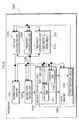
- processor 300 in the second embodiment in which part of the processor 100 in the first embodiment is modified, with reference to FIGs. 6 and 7.
- the processor 300 is different from the processor 100 in that the processor 300 changes the bus width mode individually for each instruction to be executed, depending on the number of bits in the data to be calculated under calculation instructions such as an add instruction in an application program, whereas the processor 100 was basically on an assumption that it changes the bus width mode for each application program to be executed.
- FIG. 6 is a functional block diagram of the processor 300 in the second embodiment of the present invention. It should be noted that some of the components of the processor 300 which are virtually the same as the components of the processor 100 are indicated in FIG. 6 with same characters as in the FIG. 1, and detailed explanation of those same components will be omitted.
- the processor 300 is constructed with a CMOS and includes the instruction memory 110, the instruction decode unit 320, the instruction execute unit 130, the data memory 340, the voltage controlling unit 350, the frequency controlling unit 360, and the bus width controlling unit 370, as shown in the functional block diagram in FIG. 6.
- the instruction decode unit 320 is a circuit that fetches an instruction from the instruction memory 110 and decodes them one by one, and transmits, according to the results of the decoding, a control signal to a specific circuit etc. in the instruction execute unit 130 so as to have such a specific circuit operate.
- the instruction decode unit 320 also instructs both the voltage controlling unit 350 and the frequency controlling unit 360 to change their controlling actions when a CHANGE instruction has been decoded.
- the instruction decode unit 320 detects the number of bits in the data to be calculated under the calculation instruction, and informs the bus width controlling unit 370 of the result of the detection.
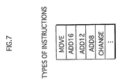
- FIG. 7 shows an example of a part of an instruction set for the processor 300.
- the MOVE instruction is an instruction that instructs a data transfer
- the ADD16 instruction is a 16-bit add instruction that instructs an addition of two pieces of 16-bit data and, as a result, an output of a piece of 16-bit data
- the ADD12 instruction is a 12-bit add instruction that instructs an addition of two pieces of 12-bit data and, as a result, an output of a piece of 12-bit data
- the ADD8 instruction is an 8-bit add instruction that instructs an addition of two pieces of 8-bit data and, as a result, an output of a piece of 8-bit data.
- the instruction set of the processor 300 it is possible to distinguish one instruction from another as either an instruction that instructs data calculation on 8-bit data, or an instruction that instructs data calculation on 12-bit data, or an instruction that instructs data calculation on 16-bit data.
- 16-bit add instruction, 12-bit add instruction, and 8-bit add instruction can be selectively used as required, for each application program individually, or for each processing in an application program individually.
- the application program sets the operation mode as the normal mode, if two or more different kinds of those 16-bit, 12-bit and 8-bit add instructions exist together in a sequence of instructions to be executed in a relatively short time with in the application program. The reason is because it takes a certain period of time to change the voltage or the clock frequency; and therefore, the performance level of execution of the application program gets degraded if there are such changes frequently. For example, it takes approximately 10 ⁇ s of time to change the voltage by 1mV.
- the instruction decode unit 320 Upon decoding a 16-bit add instruction, the instruction decode unit 320 informs the bus width controlling unit 370 that the mode is the 16-bit mode, and has the calculation unit 131 in the instruction execute unit 130 perform an addition; Upon decoding a 12-bit add instruction, the instruction decode unit 320 informs the bus width controlling unit 370 that the mode is the 12-bit mode, and has the calculation unit 131 perform an addition; Upon decoding an 8-bit add instruction, the instruction decode unit 320 informs the bus width controlling unit 370 that the mode is the 8-bit mode, and has the calculation unit 131 perform an addition.
- the data memory 340 is a cache memory and register that stores data, and includes the operation mode area 149 for storing operation modes.
- Each application program is arranged to include, before a CHANGE instruction mentioned above, a data transfer instruction for transferring such data in an external memory that indicates the operation mode to the operation mode area 149 in the data memory.
- the instruction decode unit 320 decodes a data transfer instruction and has the transfer unit 139 execute the transfer, then as a result, the operation mode area 149 stores an operation mode specified by the application program.
- the bus width controlling unit 370 includes the bus width mode area 371 that stores and retains bus width modes. Upon obtaining a result of a detection by the instruction decode unit 320 of the number of bits in data to be calculated under an instruction, the bus width controlling unit 370 stores and retains the detection result in the bus width mode area 371. Consequently, the bus width mode area 371 retains information that indicates either (i) the 16-bit mode corresponding to an instruction for calculation of 16-bit data, (ii) the 12-bit mode corresponding to an instruction for calculation of 12-bit data, or (iii) the 8-bit mode corresponding to an instruction for calculation of 8-bit data.
- the bus width controlling unit 370 refers to the bus width mode area 371, and for example, performs controlling by expressing each of the bus width modes with a 2-bit signal so that they are identifiable and informing the calculation unit 131 of a selected bus width mode.
- the voltage controlling unit 350 controls the voltages to be impressed on functional blocks in the processor. It sometimes performs controlling so that no voltage is impressed on an unused functional block, and sometimes so that a voltage level to be impressed on the calculation unit 131 would be changed according to a bus width mode selected well as the operation mode stored in the operation mode area 149, with a trigger of the instruction decode unit 320 instructing the voltage control unit 350 to change its controlling actions, or with a trigger of the change of the bus width mode in the bus width mode area 371.
- the frequency controlling unit 360 supplies clock signals to each functional block in the processor, and controls the frequencies of clock signals and the like. It sometimes performs controlling so that no clock signals are supplied to an unused functional block, and sometimes so that the frequency of clock signals to be supplied to the calculation unit 131 would be changed according to a bus width mode selected as well as the operation mode stored in the operation mode area 149, with a trigger of the instruction decode unit 320 instructing the frequency controlling unit 360 to change its controlling actions, or with a trigger of the change of the bus width mode in the bus width mode area 371.
- a 16-bit add instruction two pieces of 16-bit data are selected that are specified by certain addresses or register IDs in the data memory 340, according to an operand for the addition instruction and the like.
- the two pieces of 16-bit data selected will be placed on each set of 16-bit buses and inputted to the calculation unit 131 as srcA [15:0] andsrcB [15:0] respectively.
- a 12-bit add instruction two pieces of 12-bit data in the data memory 340 are selected, and will be inputted to the calculation unit 131 as srcA [11:0] and srcB [11:0] respectively.
- a piece of 16-bit data, namely dest [15:0] outputted by the calculation unit 131 will be stored in an area specified by a certain address or a register ID in the data memory 140 according to an operand for the addition instruction and the like;
- a 12-bit add instruction a piece of 12-bit data, namely dest [11:0] outputted by the calculation unit 131 will be stored in an area specified by a certain address or a register ID in the data memory 140 according to an operand for the addition instruction and the like;
- an 8-bit add instruction a piece of 8-bit data, namely dest [7:0] outputted by the calculation unit 131 will be stored in an area specified by a certain address or a register ID in the data memory 140 according to an operand for the addition instruction and the like.
- a carry bit signal (carry) outputted by the calculation unit 131 will be stored in what is called a flag register or the like
- processor 300 With the processor 300 arranged as above, it is possible to reduce electric power consumption in execution of application programs, depending on a number of bits required by each of the calculation instructions included therein, while maintaining the level of performance required for the execution of the application programs, even if a bus width mode is not specified within each of the application programs.
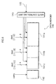
- FIG. 8 is a diagram to show a part of the data memory 140 that is capable of performing write control in the third embodiment.
- the data storing areas 141a, 141b, and 141c are an area for 8 bits, 4 bits, and 4 bits respectively, and these three data storing areas together make a 16-bit register.
- Each of the data storing areas is independent, and is arranged so that only when it receives a write signal, it will store in a storage element the data on the buses, which is a result outputted by the calculation unit 131.
- the write controlling unit 143 is a circuit that performs control for having the data outputted by the calculation unit 131 written in a storage element, at a time when the calculation unit 131 completes calculation, under the control of the instruction decode unit 120.
- the write controlling unit 143 receives the signal 183 indicating a bus width mode transmitted by the bus width controlling unit 170, and provides some or all of the data storing areas with a write signal according to the bus width mode indicated.
- the write controlling unit 143 (i) provides all of the data storing areas 141a, 141b, and 141c with a write signal if the 16-bit mode is selected, (ii) provides only the data storing areas 141a and 141b with a write signal if the 12-bit mode is selected, and (iii) provides only the data storing area 141a with a write signal if the 8-bit mode is selected.
- the modified processor which comprises the calculation unit 231 instead, which is a modification of the calculation unit 131 in the processor 100 in the first embodiment, with reference to FIG. 9.
- the bus width mode is either the 16-bit mode or the 8-bit mode
- the 8-bit mode means that a piece of 16-bit data is calculated by segments of 8 bits. It should be noted, however, that in this modifiedprocessor, it is arranged so that 16 bits of data will be effective in calculation whether the mode is the 16-bit mode or the 8-bit mode.
- FIG. 9 shows a detailed structure of the calculation unit 231 in the fourth embodiment.
- the calculation unit 231 is a circuit that performs calculation on two pieces of 16-bit data that are indicated as "srcA” and “srcB” in the drawing, and outputs a carrybit signal (carry) to indicate whether a carry has occurred or not, as well as a piece of 16-bit data indicated as "dest” in the drawing, as results of the calculation.
- the calculation unit 231 includes the input controlling unit 232, the calculators 233a and 233b, the carry transmitting unit 234, the carry controlling unit 235, the output controlling unit 236, and the clock gating controlling unit 237.
- the input controlling unit 232 is a selector that selects pieces of data to be inputted to the calculators from srcA [15:0] and srcB [15:0], according to the signal 183 indicating a bus width mode.
- the input controlling unit 232 (i) transmits srcA [7:0] and srcB [7:0] to two sets of 8-bit signal lines connected to the calculator 233a, as well as (ii) transmits srcA [15:8] and srcB [15:8] to two sets of 8-bit signal lines connected to the calculator 233b.
- the input controlling unit 232 (i) transmits srcA [7:0] and srcB [7:0] to two sets of 8-bit signal lines connected to the calculator 233a at the first clock timing, and (ii) transmits srcA [15:8] and srcB [15:8] again to the two sets of 8-bit signal lines connected to the calculator 233a at the second clock timing.
- the input controlling unit 232 receives the supply of clock signals so as to be able to input data into calculators prior to calculation, in synchronization with the calculation timing of the calculators.
- Each of the calculators 233a and 233b is a circuit that (i) fetches two pieces of data on signal lines connected with the input controlling unit 232 upon a signal clock being supplied, (ii) adds up those two pieces of data while taking account of a carry bit signal inputted to the carry-in terminal, and (iii) outputs a piece of 8-bit data and a carry bit signal as results of the calculation .
- the carry transmitting unit 234 is a circuit that inputs a carry bit signal outputted by the calculator 233a selectively either to the carry-in terminal of the calculator 233a, the carry-in terminal of the calculator 233b, or the output controlling unit 236, under the control of the carry controlling unit 235.
- the carry controlling unit 235 (i) controls the carry transmitting unit 234 to input a carry bit signal to the carry-in terminal of the calculator 233b when the 16-bit mode is selected, and (ii) controls the carry transmitting unit 234 to input a carry bit signal to the carry-in terminal of the calculator 233a at the first clock timing, and controls the carry transmitting unit 234 to input a carry bit signal to the output controlling unit 236 at the second clock timing, when the 8-bit mode is selected.
- the output controlling unit 236 is a selector that outputs pieces of data outputted by the calculators to the outside of the calculation unit 231, i.e. to the data memory, according to the signal 183 indicating a bit width mode.
- the output controlling unit 236 (i) outputs a piece of 8-bit data outputted by the calculator 233a as dest [7:0], and outputs a piece of 8-bit data outputted by the calculator 233b as dest [15:8], and a carry bit signal outputted by the calculator 233b as "carry”.
- the output controlling unit 236 receives two pieces of 8-bit data outputted by the calculator 233a respectively at the clock timing of the first addition and at the clock timing of the second addition, and outputs the first 8-bit data as dest [7:0], and the second 8-bit data as dest [15:8], and further outputs the carry bit signal transmitted by the carry transmitting unit 234 as "carry" at the following clock timing.
- the clock gating controlling unit 237 is a circuit that transmits the clock signal (CLK) outputted from the frequency controlling unit 160 to both of the calculators 233a and 233b as "CLKA” and "CLKB” respectively when the 16-bit mode is selected, and transmits the clock signal only to the calculator 233a, and cuts off the supply of clock signals to the calculator 233b, when the 8-bit mode is selected.
- CLK clock signal
- the time required for data calculation in the 8-bit mode is approximately twice as long as the time required for data calculation in the 16-bit mode; however, it is possible to reduce electric power consumption because of the calculator 233b not operating in the 8-bit mode.
- the 8-bit mode it is not necessary to transmit a carry bit signal between the calculators with one clock, but it is sufficient if a carry bit signal is transmitted with two clocks; therefore, it is possible to apply the control performed by the voltage controlling unit 150 and the frequency controlling unit 160 according to an operation mode, which was discussed in the section of the first embodiment. Consequently, when the 8-bit mode is combined with the low electric power consumption mode, the data calculation speed stays at approximately half of what it is in the 16-bit mode, and electric power consumption in data calculation is lower. When the 8-bit mode is combined with the high speed mode, the data calculation speed is higher than approximately half of what it is in the 16-bit mode.
- microprocessor of the present invention has been so far explained based on the first through fourth embodiments. Needless to say, the present invention is not limited to these embodiments. More specifically, the following shouldbe noted:
Landscapes
- Engineering & Computer Science (AREA)
- Theoretical Computer Science (AREA)
- Software Systems (AREA)
- General Physics & Mathematics (AREA)
- Physics & Mathematics (AREA)
- General Engineering & Computer Science (AREA)
- Mathematical Analysis (AREA)
- Mathematical Optimization (AREA)
- Pure & Applied Mathematics (AREA)
- Computational Mathematics (AREA)
- Microcomputers (AREA)
- Power Sources (AREA)
- Executing Machine-Instructions (AREA)
- Complex Calculations (AREA)
Applications Claiming Priority (2)
| Application Number | Priority Date | Filing Date | Title |
|---|---|---|---|
| JP2001386710A JP2003186567A (ja) | 2001-12-19 | 2001-12-19 | マイクロプロセッサ |
| JP2001386710 | 2001-12-19 |
Publications (2)
| Publication Number | Publication Date |
|---|---|
| EP1321850A2 true EP1321850A2 (de) | 2003-06-25 |
| EP1321850A3 EP1321850A3 (de) | 2007-11-21 |
Family
ID=19187963
Family Applications (1)
| Application Number | Title | Priority Date | Filing Date |
|---|---|---|---|
| EP02258677A Withdrawn EP1321850A3 (de) | 2001-12-19 | 2002-12-17 | Mikroprozessor mit Rechnungseinheit |
Country Status (6)
| Country | Link |
|---|---|
| US (1) | US7020787B2 (de) |
| EP (1) | EP1321850A3 (de) |
| JP (1) | JP2003186567A (de) |
| KR (1) | KR20030051380A (de) |
| CN (1) | CN1286005C (de) |
| TW (1) | TWI266237B (de) |
Families Citing this family (13)
| Publication number | Priority date | Publication date | Assignee | Title |
|---|---|---|---|---|
| JP4412905B2 (ja) * | 2003-01-28 | 2010-02-10 | パナソニック株式会社 | 低電力動作制御装置、およびプログラム最適化装置 |
| US20060206689A1 (en) * | 2003-08-07 | 2006-09-14 | Matsushita Electric Industrial Co., Ltd. | Processor integrated circuit and product development method using the processor integrated circuit |
| US7496776B2 (en) * | 2003-08-21 | 2009-02-24 | International Business Machines Corporation | Power throttling method and apparatus |
| JP4367225B2 (ja) * | 2004-05-11 | 2009-11-18 | ソニー株式会社 | 半導体集積回路 |
| US7886131B1 (en) * | 2006-08-14 | 2011-02-08 | Marvell International Ltd. | Multithread processor with thread based throttling |
| US9141392B2 (en) * | 2010-04-20 | 2015-09-22 | Texas Instruments Incorporated | Different clock frequencies and stalls for unbalanced pipeline execution logics |
| TWM393112U (en) * | 2010-06-02 | 2010-11-21 | Sentelic Corp | digital signal processor |
| KR20110137973A (ko) * | 2010-06-18 | 2011-12-26 | 삼성전자주식회사 | 컴퓨터시스템 및 그 제어방법 |
| US20120265904A1 (en) * | 2011-06-23 | 2012-10-18 | Renesas Electronics Corporation | Processor system |
| JP5791462B2 (ja) * | 2011-10-24 | 2015-10-07 | 三菱電機株式会社 | 半導体管理システム及び半導体管理方法 |
| CN108733352B (zh) * | 2017-04-25 | 2021-06-11 | 上海寒武纪信息科技有限公司 | 支持向量排序的装置、方法及应用 |
| CN108416431B (zh) * | 2018-01-19 | 2021-06-01 | 上海兆芯集成电路有限公司 | 神经网络微处理器与宏指令处理方法 |
| CA3225836A1 (en) * | 2021-07-23 | 2023-01-26 | Etienne DUMESNIL | Apparatus and method for energy-efficient and accelerated processing of an arithmetic operation |
Citations (7)
| Publication number | Priority date | Publication date | Assignee | Title |
|---|---|---|---|---|
| EP0505884A2 (de) * | 1991-03-29 | 1992-09-30 | Hitachi, Ltd. | Arithmetische Schaltung für adaptive Filter und Echoauslöscher |
| EP0679992A1 (de) * | 1994-04-26 | 1995-11-02 | Advanced Micro Devices, Inc. | Prozessorarchitektur für gemischte Funktionseinheiten |
| US5636351A (en) * | 1993-11-23 | 1997-06-03 | Hewlett-Packard Company | Performance of an operation on whole word operands and on operations in parallel on sub-word operands in a single processor |
| EP0845741A2 (de) * | 1996-11-29 | 1998-06-03 | Matsushita Electric Industrial Co., Ltd. | Prozessor mit verbessertem Rundungsprozess |
| US5884092A (en) * | 1995-10-09 | 1999-03-16 | Hitachi, Ltd. | System for maintaining fixed-point data alignment within a combination CPU and DSP system |
| US6131154A (en) * | 1991-06-24 | 2000-10-10 | Hitachi, Ltd. | Microcomputer having variable bit width area for displacement |
| US6308252B1 (en) * | 1999-02-04 | 2001-10-23 | Kabushiki Kaisha Toshiba | Processor method and apparatus for performing single operand operation and multiple parallel operand operation |
Family Cites Families (8)
| Publication number | Priority date | Publication date | Assignee | Title |
|---|---|---|---|---|
| JP2762670B2 (ja) * | 1990-03-30 | 1998-06-04 | 松下電器産業株式会社 | データ処理装置 |
| EP1229440B1 (de) * | 1993-05-27 | 2007-05-02 | Matsushita Electric Industrial Co., Ltd. | Programmumsetzungseinheit und verbesserter Prozessor für Adressierung |
| JP2832899B2 (ja) * | 1993-05-31 | 1998-12-09 | 松下電器産業株式会社 | データ処理装置およびデータ処理方法 |
| JP3520611B2 (ja) * | 1995-07-06 | 2004-04-19 | 株式会社日立製作所 | プロセッサの制御方法 |
| US5918058A (en) * | 1997-02-20 | 1999-06-29 | Arm Limited | Routing of clock signals in a data processing circuit with a power saving mode of operation |
| US6219796B1 (en) * | 1997-12-23 | 2001-04-17 | Texas Instruments Incorporated | Power reduction for processors by software control of functional units |
| US6141283A (en) * | 1999-04-01 | 2000-10-31 | Intel Corporation | Method and apparatus for dynamically placing portions of a memory in a reduced power consumption state |
| US6425086B1 (en) * | 1999-04-30 | 2002-07-23 | Intel Corporation | Method and apparatus for dynamic power control of a low power processor |
-
2001
- 2001-12-19 JP JP2001386710A patent/JP2003186567A/ja active Pending
-
2002
- 2002-12-17 EP EP02258677A patent/EP1321850A3/de not_active Withdrawn
- 2002-12-18 TW TW091136558A patent/TWI266237B/zh not_active IP Right Cessation
- 2002-12-18 US US10/323,419 patent/US7020787B2/en not_active Expired - Fee Related
- 2002-12-18 KR KR1020020081016A patent/KR20030051380A/ko not_active Application Discontinuation
- 2002-12-19 CN CNB021570299A patent/CN1286005C/zh not_active Expired - Fee Related
Patent Citations (7)
| Publication number | Priority date | Publication date | Assignee | Title |
|---|---|---|---|---|
| EP0505884A2 (de) * | 1991-03-29 | 1992-09-30 | Hitachi, Ltd. | Arithmetische Schaltung für adaptive Filter und Echoauslöscher |
| US6131154A (en) * | 1991-06-24 | 2000-10-10 | Hitachi, Ltd. | Microcomputer having variable bit width area for displacement |
| US5636351A (en) * | 1993-11-23 | 1997-06-03 | Hewlett-Packard Company | Performance of an operation on whole word operands and on operations in parallel on sub-word operands in a single processor |
| EP0679992A1 (de) * | 1994-04-26 | 1995-11-02 | Advanced Micro Devices, Inc. | Prozessorarchitektur für gemischte Funktionseinheiten |
| US5884092A (en) * | 1995-10-09 | 1999-03-16 | Hitachi, Ltd. | System for maintaining fixed-point data alignment within a combination CPU and DSP system |
| EP0845741A2 (de) * | 1996-11-29 | 1998-06-03 | Matsushita Electric Industrial Co., Ltd. | Prozessor mit verbessertem Rundungsprozess |
| US6308252B1 (en) * | 1999-02-04 | 2001-10-23 | Kabushiki Kaisha Toshiba | Processor method and apparatus for performing single operand operation and multiple parallel operand operation |
Also Published As
| Publication number | Publication date |
|---|---|
| US7020787B2 (en) | 2006-03-28 |
| CN1286005C (zh) | 2006-11-22 |
| KR20030051380A (ko) | 2003-06-25 |
| US20030135779A1 (en) | 2003-07-17 |
| EP1321850A3 (de) | 2007-11-21 |
| CN1427336A (zh) | 2003-07-02 |
| JP2003186567A (ja) | 2003-07-04 |
| TW200306493A (en) | 2003-11-16 |
| TWI266237B (en) | 2006-11-11 |
Similar Documents
| Publication | Publication Date | Title |
|---|---|---|
| US5630143A (en) | Microprocessor with externally controllable power management | |
| US6978390B2 (en) | Pipelined data processor with instruction-initiated power management control | |
| US7020787B2 (en) | Microprocessor | |
| US8341436B2 (en) | Method and system for power-state transition controllers | |
| JP2006509290A (ja) | マイクロプロセッサ電力消費低減のためのレジスタファイルゲーティング | |
| JP2000047872A (ja) | 低消費電力動作機能を備えたマイクロプロセッサ | |
| KR20070061086A (ko) | 동적 전압 스케일링을 적용한 고효율 프로세서 | |
| KR20070039079A (ko) | 명령어 처리 회로 | |
| US5603037A (en) | Clock disable circuit for translation buffer | |
| US6496888B1 (en) | Incorporation of bus ratio strap options in chipset logic | |
| JP4689087B2 (ja) | 情報処理装置及び省電力移行制御方法 | |
| US20070271440A1 (en) | Computer processor architecture selectively using finite-state-machine for control code execution | |
| EP0828212B1 (de) | Mikroprozessor mit hardwaregesteuerter Leistungsverwaltung und auswählbaren Eingangs-/Ausgangssteuerungssteckerstiften und Verfahren hierfür | |
| US6993674B2 (en) | System LSI architecture and method for controlling the clock of a data processing system through the use of instructions | |
| US5375209A (en) | Microprocessor for selectively configuring pinout by activating tri-state device to disable internal clock from external pin | |
| JP4800582B2 (ja) | 演算処理装置 | |
| JP2002508562A (ja) | ジッターのない命令の実行 | |
| WO1996037893A1 (en) | Partitioned decoder circuit for low power operation | |
| JPH10340129A (ja) | 電子システムにおける電力使用量を制御する回路および方法 | |
| US7290153B2 (en) | System, method, and apparatus for reducing power consumption in a microprocessor | |
| JPH11328011A (ja) | 記憶制御装置および情報処理機器 | |
| JPH03168832A (ja) | 分散型マイクロプログラム制御方式 | |
| JPH01276326A (ja) | プログラム処理回路 | |
| JPH09128235A (ja) | 5段パイプライン構造のプログラマブルコントローラ |
Legal Events
| Date | Code | Title | Description |
|---|---|---|---|
| PUAI | Public reference made under article 153(3) epc to a published international application that has entered the european phase |
Free format text: ORIGINAL CODE: 0009012 |
|
| AK | Designated contracting states |
Designated state(s): AT BE BG CH CY CZ DE DK EE ES FI FR GB GR IE IT LI LU MC NL PT SE SI SK TR |
|
| AX | Request for extension of the european patent |
Extension state: AL LT LV MK RO |
|
| PUAL | Search report despatched |
Free format text: ORIGINAL CODE: 0009013 |
|
| AK | Designated contracting states |
Kind code of ref document: A3 Designated state(s): AT BE BG CH CY CZ DE DK EE ES FI FR GB GR IE IT LI LU MC NL PT SE SI SK TR |
|
| AX | Request for extension of the european patent |
Extension state: AL LT LV MK RO |
|
| AKX | Designation fees paid | ||
| REG | Reference to a national code |
Ref country code: DE Ref legal event code: 8566 |
|
| STAA | Information on the status of an ep patent application or granted ep patent |
Free format text: STATUS: THE APPLICATION IS DEEMED TO BE WITHDRAWN |
|
| 18D | Application deemed to be withdrawn |
Effective date: 20080522 |
|
| RAP1 | Party data changed (applicant data changed or rights of an application transferred) |
Owner name: PANASONIC CORPORATION |