EP1320168A1 - Power switch for battery protection - Google Patents
Power switch for battery protection Download PDFInfo
- Publication number
- EP1320168A1 EP1320168A1 EP01480132A EP01480132A EP1320168A1 EP 1320168 A1 EP1320168 A1 EP 1320168A1 EP 01480132 A EP01480132 A EP 01480132A EP 01480132 A EP01480132 A EP 01480132A EP 1320168 A1 EP1320168 A1 EP 1320168A1
- Authority
- EP
- European Patent Office
- Prior art keywords
- fet
- battery
- bulk
- fet switch
- coupled
- Prior art date
- Legal status (The legal status is an assumption and is not a legal conclusion. Google has not performed a legal analysis and makes no representation as to the accuracy of the status listed.)
- Withdrawn
Links
Images



Classifications
-
- H—ELECTRICITY
- H02—GENERATION; CONVERSION OR DISTRIBUTION OF ELECTRIC POWER
- H02J—ELECTRIC POWER NETWORKS; CIRCUIT ARRANGEMENTS OR SYSTEMS FOR SUPPLYING OR DISTRIBUTING ELECTRIC POWER; SYSTEMS FOR STORING ELECTRIC ENERGY
- H02J7/00—Circuit arrangements for charging or discharging batteries or for supplying loads from batteries
- H02J7/60—Circuit arrangements for charging or discharging batteries or for supplying loads from batteries including safety or protection arrangements
- H02J7/663—Circuit arrangements for charging or discharging batteries or for supplying loads from batteries including safety or protection arrangements using battery or load disconnect circuits
-
- H—ELECTRICITY
- H02—GENERATION; CONVERSION OR DISTRIBUTION OF ELECTRIC POWER
- H02J—ELECTRIC POWER NETWORKS; CIRCUIT ARRANGEMENTS OR SYSTEMS FOR SUPPLYING OR DISTRIBUTING ELECTRIC POWER; SYSTEMS FOR STORING ELECTRIC ENERGY
- H02J7/00—Circuit arrangements for charging or discharging batteries or for supplying loads from batteries
- H02J7/60—Circuit arrangements for charging or discharging batteries or for supplying loads from batteries including safety or protection arrangements
- H02J7/61—Circuit arrangements for charging or discharging batteries or for supplying loads from batteries including safety or protection arrangements against overcharge
-
- H—ELECTRICITY
- H02—GENERATION; CONVERSION OR DISTRIBUTION OF ELECTRIC POWER
- H02J—ELECTRIC POWER NETWORKS; CIRCUIT ARRANGEMENTS OR SYSTEMS FOR SUPPLYING OR DISTRIBUTING ELECTRIC POWER; SYSTEMS FOR STORING ELECTRIC ENERGY
- H02J7/00—Circuit arrangements for charging or discharging batteries or for supplying loads from batteries
- H02J7/60—Circuit arrangements for charging or discharging batteries or for supplying loads from batteries including safety or protection arrangements
- H02J7/63—Circuit arrangements for charging or discharging batteries or for supplying loads from batteries including safety or protection arrangements against overdischarge
Definitions
- the invention relates to a circuit for protecting a battery, and more particularly, to a circuit for controlling the charging, discharging, and protection of a rechargeable battery.
- Rechargeable batteries are used in a variety of applications of portable electronic devices.
- rechargeable batteries are used for portable phones.
- Several types of batteries are used in the art, most notably those comprising lithium ion or Li + .
- the battery must be protected from excessive charging voltage during recharging and from over discharging while supplying the appliance.
- a rechargeable battery 10 is configured such that it can source energy to a load 34 or can be recharged by a charger source 38.
- Two MOSFET switches N1 18 and N2 26 are used to control the flow of current into (charging) and out of (discharging) the battery.
- the control circuit 14 controls the ON and OFF state of the switches 18 and 26.
- the switches comprise discrete devices.
- Each switch 18 and 26 contains a parasitic bulk-to-drain diode D1 22 and D2 30. By coupling each switch in an opposite manner, each of the parasitic diodes 22 and 30 conducts current in a different direction.
- both of the switches are ON. However, if the control circuit 14 detects an over charging voltage from VBATT to GND, then the control circuit turns OFF the switch N1. Since the parasitic diode D1 22 also blocks current flow into the battery, the battery stops charging. In the case of an over discharging condition, the control circuit 14 would detect a too low battery voltage from VBATT to GND. The other switch N2 26 would be turned OFF. In this case, the parasitic diode D2 30 blocks current flow out of the battery 10.
- the prior art circuit has at least two disadvantages. First, two FET switches are required in order to obtain two-directional switching capability. Therefore, the series resistance of the battery pack is increased. Second, the use of discrete components increases the manufacturing cost and space requirements for the protection circuit.
- U.S. Patent 6,246,214 to Oglesbee shows a battery protection circuit having only one MOSFET switch. A voltage protection circuit is used to limit the voltage so that a single MOSFET can be used for two directional current control.
- U.S. Patent 5,063,471 to Park discloses a battery protection circuit.
- U.S. Patent 5,789,900 to Hasegawa et al discloses a battery protection circuit showing two MOSFETs having back-to-back diodes.
- U.S. Patent 6,160,381 to Peterzell discloses a battery pack protection circuit. Two MOS switches are used.
- Patent 5,081,371 to Wong describes a charge pump circuit where back gate biased MOSFETs are used.
- U.S. Patent 5,933,046 to Ramet et al teaches an analog switch formed from a MOSFET that has a switchable bulk connection.
- a principal object of the present invention is to provide an effective and very manufacturable circuit for protecting a battery.
- a further object of the present invention is to provide a battery protection circuit for controlling charging and discharging of a battery.
- a still further object of the present invention is to control both charging and discharging via a single FET having a switchable bulk connection.
- Another still further object of the present invention is to cascade switchable bulk FET devices to increase the voltage range of the circuit.
- Yet another still further object of the present invention is to charge the middle node between cascaded FET devices to improve performance.
- Another still further object of the present invention is to form the switchable bulk FET devices using either NMOS or PMOS devices.
- a battery charging, discharging, and protection circuit comprises, first, a FET switch having gate, source, drain, and bulk.
- the FET switch may comprise either a NMOS device or a PMOS device.
- the source is coupled to a load terminal, and the drain is coupled to a battery terminal.
- a means of controlling the FET switch gate and the bulk is included.
- the FET switch gate voltage determines the OFF and ON state of said FET switch.
- the FET bulk is switchably coupled between the battery terminal and the load terminal.
- a battery charging, discharging, and protection circuit is achieved.
- the circuit comprises, first, a first FET switch having gate, source, drain, and bulk.
- the drain is coupled to a battery terminal.
- a second FET switch having gate, source, drain, and bulk is used.
- the drain is coupled to the first NMOS FET switch source to thereby form a mid node.
- the source is coupled to a load terminal.
- a means of controlling the first and second FET gates and the switchable bulks is used.
- the first and second FET switch gates voltages determine the OFF and ON states of the first and second FET switches.
- the first FET bulk is switchably coupled between the battery terminal and the mid node.
- the second FET bulk is switchably coupled between the mid node and the load terminal.
- the preferred embodiments disclose a novel circuit for protecting a battery.
- the circuit uses a novel, single FET device having a switchable bulk connection to achieve control of both charging and discharging current. Additional switchable bulk FET devices may be cascaded to increase the operating range of the circuit. It should be clear to those experienced in the art that the present invention can be applied and extended without deviating from the scope of the present invention.
- a battery 70 preferably comprises a rechargeable battery.
- the circuit is configured to allow the battery 70 to source current to a load 88 or to be recharged by a charging source 90.
- the battery 70 preferably comprises a two-terminal device. In the illustration, the positive terminal is labeled VBATT 92. The negative terminal is labeled GND 96.
- the battery protection circuit comprises, first, a FET switch N1 78.
- a FET switch N1 78 In this version of the first preferred embodiment, a single FET switch and, more preferably, a NMOS FET switch 78 is used.
- An alternative version, showing a PMOS FET switch is shown as Fig. 6.
- the FET switch N1 78 is preferably fabricated in a standard MOS process such that the control circuit 74 and the switch N1 78 can be fabricated on the same substrate.
- the NMOS FET N1 78 must be fabricated in a well (p-type) that can be isolated from the semiconductor substrate. In this way, the well, or bulk, of the device can be biased independently of the substrate.
- the NMOS FET switch N1 78 has gate, drain, source, and bulk connections.
- the source is coupled to the external load terminal GNDOUT 94 that is further coupled to an external device, such as a portable phone circuit or a charging source 90.
- the drain is coupled to the negative battery terminal GND 96.
- the gate is coupled to the control circuit 74.
- the control circuit 74 monitors the battery 70 voltage, from VBATT 92 to GND 96, to protect the battery from over charging and from over discharging.
- a most important feature of the present invention is the configuration of the bulk connection of the NMOS FET N1 78.
- the bulk is not coupled to either the source or the drain as in the prior art. Further, the bulk is not coupled to any fixed voltage level. Rather, a switchable bulk is used. In particular, the bulk is switchable between the negative battery terminal 96 and the load terminal GNDOUT 94.
- a first switch SW1 82 allows the bulk to be coupled to or de-coupled from the negative battery terminal 96.
- a second switch SW2 86 allows the bulk to be coupled to or de-coupled from the load terminal GNDOUT 94.
- the NMOS FET switch N1 78 is turned ON by the control circuit 74.
- the bulk is coupled to the load terminal GNDOUT 94 by closing SW2 86 and opening SW1 82.
- the gate drive of the control circuit can create a minimum ON resistance for NMOS switch N1.
- the charging source 90 can then source current into the battery to fully recharge it.
- the control circuit 74 turns OFF the NMOS FET switch N1 78 to stop charging current flow. Because the bulk is coupled to GNDOUT 94, a reverse biased p-n diode formed by the bulk and the drain prevents charging current flow from the negative battery terminal 96 to GNDOUT 94.
- the NMOS FET switch N1 78 is turned ON by the control circuit 74.
- the bulk is coupled to the negative battery terminal GND 96 by closing the switch SW1 82 while opening the switch SW2 86.
- Discharging current flows through N1 78 from GNDOUT 94 to GND 96. If an over discharge occurs, the battery voltage will drop below a pre-determined value.
- the NMOS FET switch N1 78 is turned OFF by the control circuit 74. However, the bulk remains coupled to the negative terminal GND 96. The bulk-to-source diode is reverse biased and blocks any forward current flow.
- the battery may be charging during an over discharge state.
- the over discharge state the battery has been excessively discharged during a previous operation.
- the charging current should be limited to protect the battery. Therefore, the gate of N1 78 is coupled to the drain node GND 96 such that the device operates as a MOS diode.
- the second condition the battery may be discharging in an overcharged stated. In this state, the battery has been overcharged.
- the current should again be limited to protect the battery. Therefore, the gate of N1 78 is coupled to the source node GNDOUT 94 such that the device again operates as a MOS diode, in this case for forward current.
- a PMOS FET is used for the switch P1 408.
- the NMOS transistor provides much lower ON resistance and is, therefore, the logical choice for a drive switch.
- the present invention is easily extendable to use a PMOS FET as the switch.
- the PMOS FET switch 408 has source coupled to the load terminal LOAD 428 and drain coupled to the positive battery terminal VBATT 420. The gate is controlled by the control circuit 404. The bulk is again switchable.
- the bulk is switched between the positive battery terminal 420 and LOAD 428 by switches SW1 412 and SW2 416, respectively.
- the bulk of the PMOS device must be a well (n-type) that can be biased independently of the substrate.
- the operating table for the single PMOS FET version is shown as Table 2 below and operates as the NMOS FET version operates. Operating Conditions for Single PMOS FET Circuit. Operating Condition FET Condition Bulk Coupling Charging ON SW2 ON Over Charging OFF SW2 ON Charging in Over Discharge State MOS Diode SW2 ON Discharging ON SW1 ON Over Discharging OFF SW1 ON Discharging in Over Charge State MOS Diode SW1 ON
- the PMOS FET switch P1 408 is ON while the bulk is biased to the output LOAD 428 by turning ON SW2 416 and turning OFF SW1 412. This enables the switch P1 408 to exhibit minimum ON resistance while not turning on the bulk-to-drain diode and risking latchup. If an over charging is detected, the PMOS FET is turned OFF while the bulk remains at LOAD. The current is thereby blocked by both the switching channel and the reverse biased p-n diode.
- P1 408 is ON while the bulk is biased to the positive battery terminal 420 by turning ON SW1 412 and turning OFF SW2 416. Again, this minimizes the ON resistance.
- P1 is turned OFF and the bulk is left at VBATT to_insure no forward current. The charging during over discharge condition and the discharging during over charge conditions operate the same as for the NMOS case.
- a second preferred embodiment of the present invention is illustrated.
- two NMOS FET switches N1 108 and N2 120 are used.
- N1 and N2 are cascaded to provide a combined switch having a larger operating voltage range than is available with a single switch.
- the battery charging source 136 is capable of generating a larger voltage than the battery 100.
- the single FET switch is turned OFF, the voltage difference between the charger 90 and the battery 70 must be sustained across the switch.
- the voltage range of the switch is limited by the drain-to-bulk reverse breakdown as given be the manufacturing process. This breakdown voltage may be about 7 Volts, for example. This means that the charger 90 design must be limited to not generate a voltage greater than the battery 70 voltage plus about 7 Volts.
- the first FET switch N1 has gate, source, drain, and bulk.
- the drain is coupled to the negative battery terminal, GND 148.
- the bulk is switchably coupled between the negative battery terminal GND 148 and a middle node MID 142 between the cascaded FET devices N1 108 and N2 120.
- the second FET switch N2 120 has gate, source, drain, and bulk. The drain is coupled to the first FET switch N1 drain at the mid node MID 142.
- the source is coupled to the_load terminal node GNDOUT 144.
- the bulk of N2 120 is switchably coupled between MID 142 and the load terminal GNDOUT 144.
- the control circuit CONTROL 104 drives the gates of N1 108 and N2 120 and the bulk switches SW1 112, SW2 116, SW3 124, and SW4 128.
- Table 3 The operating table for the second embodiment using cascaded NMOS FET switches is shown as Table 3 below. Operating modes for Cascaded NMOS Circuit.
- the operating concept of the single NMOS FET is extended to create the cascaded switch.
- both of the transistors N1 and N2 are ON.
- the bulk of N1 108 is coupled to the MID node 142 by turning ON SW2 116.
- the bulk of N2 120 is coupled to the load terminal GNDOUT 144 by turning ON SW4 128.
- the control circuit 104 turns OFF both switches N1 and N2 to interrupt current flow.
- the configuration of the bulks presents a series of reversed biased p-n junctions between the negative battery terminal GND 148 and the load terminal GNDOUT to thereby block charging current.
- the use of two NMOS devices allows the voltage difference between GND 148 and GNDOUT 144 to drop across two bulk-to-drain diodes and thereby increases the operating range when compared to a single transistor approach.
- control circuit 104 turns OFF N2 120.
- the bulk of N1 108 is coupled to GND 148 by SW1 112 and the bulk of N2 120 is coupled to MID 142 by SW3 124.
- the cascaded circuit works in a similar mode as the single FET circuit. Note that the first transistor N1 108 is held ON for both cases. However, the second transistor N2 120 is biased to the MOS diode case to protect the battery as in the single FET circuit.
- a PMOS version of the second embodiment cascade circuit is shown.
- two PMOS FET switches P1 508 and P2 520 are connected is series.
- the bulk for the first PMOS FET P1 508 is switched between the positive battery terminal VBATT 532 and the MID node 534.
- the bulk of the second PMOS FET P2 520 is switched between the MID node 534 and the load terminal LOAD 540.
- the operating table for the PMOS version of the cascaded circuit is shown below in Table 4 and is the same as that for the cascaded NMOS version. Operating modes for Cascaded PMOS Circuit.
- both P1 508 and P2 520 are ON.
- the bulk of P1 is coupled to MID 534 while the bulk of P2 520 is coupled to LOAD 540 to minimize the ON resistance of the switches.
- both P1 and P2 are turned OFF by the control circuit 504.
- the bulk of P1 remains at MID while the bulk of P2 remains at LOAD. This creates a series of reverse biased p-n diodes between VBATT 532 and the high voltage LOAD 540 to block current flow into the battery 500.
- P1 and P2 are ON.
- the bulk of P1 is biased to VBATT while the bulk of P2 is biased to MID to reduce ON resistance.
- P2 is turned OFF.
- the bulk of P1 is kept at VBATT 532 while the bulk of P2 is kept at MID 534. This presents a series of reverse biased p-n diodes between VBATT and LOAD.
- the cascaded switching configuration of the second embodiment may be extended to three or more switches if needed to create adequate operating voltage.
- a problem that the may occur with the cascaded switch configuration is the floating of the MID node when both of the FET switches are OFF.
- the bulk of N1 is coupled to MID 142 and the bulk of N2 is coupled to GNDOUT 144. Because the bulk-drain p-n diodes are reverse biased, the bulk of N1, which is coupled to MID, is actually floating.
- a non-uniform voltage distribution between the two bulk-drain diodes may exist and could cause one of the diodes to conduct.
- a voltage divider Z 1 232 and Z 2 236 between the positive battery terminal VBATT 248 and the load terminal GNDOUT 252.
- the purpose of the voltage divider is to provide a means of insuring that the voltage difference is evenly split between each bulk-drain diode so that the full operating range is achieved without turning on the parasitic vertical npn.
- the voltage divider Z 1 232 and Z 2 236 may comprise, for example, two resistors of equal value.
- the addition of the voltage divider to steer the bulk potentials may also be added to the PMOS version of the cascaded switch circuit shown in Fig. 7.
- switches SW5 and SW6 are added to allow the biasing voltage to be switched ON and OFF as needed.
- the operating table for third embodiment including the voltage divider is shown as Table 5 below. The voltage divider is only coupled to the MID node when the circuit is in the charging mode. Note that the same operating table applies to both NMOS and PMOS versions. Operating modes for Cascaded Circuit including Voltage Divider.
- a battery control and protection circuit 300 for a rechargeable battery is shown.
- the circuit 300 may comprise a single monolithic IC or a combination of IC chips and discrete components. Circuits are included to detect over voltage and current conditions.
- the logic block 320 uses these inputs to control the FET block 310 which comprises either a single FET or cascaded FET devices as disclosed in the present invention.
- the present invention provides an effective and very manufacturable circuit for protecting a battery.
- the battery protection circuit controls charging and discharging of a battery. Both charging and discharging is controlled via a single FET having a switchable bulk connection.
- Switchable bulk FET devices may be cascaded to increase the voltage range of the circuit.
- the switchable bulk FET devices may comprise either NMOS or PMOS devices.
- the middle node between cascaded FET devices is steered to a known voltage during over charging to further improve performance.
- the novel circuit provides an effective and manufacturable alternative to the prior art.
Landscapes
- Engineering & Computer Science (AREA)
- Power Engineering (AREA)
- Charge And Discharge Circuits For Batteries Or The Like (AREA)
Abstract
A battery charging, discharging, and protection circuit which comprises,
first, a FET switch having gate, source, drain, and bulk. The FET switch may
comprise either a NMOS device or a PMOS device. The source is coupled to a
load terminal, and the drain is coupled to a battery terminal. Second, a means of
controlling the FET switch gate and the bulk is included. The FET switch gate
voltage determines the OFF and ON state of said FET switch. The bulk is
switchably coupled between the battery terminal and the load terminal. A
cascaded version is disclosed.
Description
- The invention relates to a circuit for protecting a battery, and more particularly, to a circuit for controlling the charging, discharging, and protection of a rechargeable battery.
- Rechargeable batteries are used in a variety of applications of portable electronic devices. In particular, rechargeable batteries are used for portable phones. Several types of batteries are used in the art, most notably those comprising lithium ion or Li+. For optimum battery life and performance, the battery must be protected from excessive charging voltage during recharging and from over discharging while supplying the appliance.
- Referring now to Fig. 1, an exemplary prior art battery protection circuit. A
rechargeable battery 10 is configured such that it can source energy to aload 34 or can be recharged by acharger source 38. TwoMOSFET switches N1 18 andN2 26 are used to control the flow of current into (charging) and out of (discharging) the battery. Thecontrol circuit 14 controls the ON and OFF state of theswitches switch drain diode D1 22 andD2 30. By coupling each switch in an opposite manner, each of theparasitic diodes - During normal charging or discharging of the
battery 10, both of the switches are ON. However, if thecontrol circuit 14 detects an over charging voltage from VBATT to GND, then the control circuit turns OFF the switch N1. Since theparasitic diode D1 22 also blocks current flow into the battery, the battery stops charging. In the case of an over discharging condition, thecontrol circuit 14 would detect a too low battery voltage from VBATT to GND. Theother switch N2 26 would be turned OFF. In this case, theparasitic diode D2 30 blocks current flow out of thebattery 10. - The prior art circuit has at least two disadvantages. First, two FET switches are required in order to obtain two-directional switching capability. Therefore, the series resistance of the battery pack is increased. Second, the use of discrete components increases the manufacturing cost and space requirements for the protection circuit.
- Several prior art inventions describe battery protection circuits and devices related to bulk switching. U.S. Patent 6,246,214 to Oglesbee shows a battery protection circuit having only one MOSFET switch. A voltage protection circuit is used to limit the voltage so that a single MOSFET can be used for two directional current control. U.S. Patent 5,063,471 to Park discloses a battery protection circuit. U.S. Patent 5,789,900 to Hasegawa et al discloses a battery protection circuit showing two MOSFETs having back-to-back diodes. U.S. Patent 6,160,381 to Peterzell discloses a battery pack protection circuit. Two MOS switches are used. U.S. Patent 5,081,371 to Wong describes a charge pump circuit where back gate biased MOSFETs are used. U.S. Patent 5,933,046 to Ramet et al teaches an analog switch formed from a MOSFET that has a switchable bulk connection.
- A principal object of the present invention is to provide an effective and very manufacturable circuit for protecting a battery.
- A further object of the present invention is to provide a battery protection circuit for controlling charging and discharging of a battery.
- A still further object of the present invention is to control both charging and discharging via a single FET having a switchable bulk connection.
- Another still further object of the present invention is to cascade switchable bulk FET devices to increase the voltage range of the circuit.
- Yet another still further object of the present invention is to charge the middle node between cascaded FET devices to improve performance.
- Another still further object of the present invention is to form the switchable bulk FET devices using either NMOS or PMOS devices.
- In accordance with the objects of this invention, a battery charging, discharging, and protection circuit is achieved. The circuit comprises, first, a FET switch having gate, source, drain, and bulk. The FET switch may comprise either a NMOS device or a PMOS device. The source is coupled to a load terminal, and the drain is coupled to a battery terminal. Second, a means of controlling the FET switch gate and the bulk is included. The FET switch gate voltage determines the OFF and ON state of said FET switch. The FET bulk is switchably coupled between the battery terminal and the load terminal.
- Also in accordance with the objects of the present invention, a battery charging, discharging, and protection circuit is achieved. The circuit comprises, first, a first FET switch having gate, source, drain, and bulk. The drain is coupled to a battery terminal. Second, a second FET switch having gate, source, drain, and bulk is used. The drain is coupled to the first NMOS FET switch source to thereby form a mid node. The source is coupled to a load terminal. Finally, a means of controlling the first and second FET gates and the switchable bulks is used. The first and second FET switch gates voltages determine the OFF and ON states of the first and second FET switches. The first FET bulk is switchably coupled between the battery terminal and the mid node. The second FET bulk is switchably coupled between the mid node and the load terminal.
- In the accompanying drawings forming a material part of this description, there is shown:
- Fig. 1 illustrates a prior art battery protection circuit.
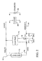
- Fig. 2 illustrates a first preferred embodiment of the battery protection circuit of the present invention where the FET switch is NMOS.
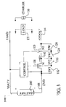
- Fig. 3 illustrates a second preferred embodiment of the battery protection circuit of the present invention where two NMOS switches are used for greater operating range.
- Fig. 4 illustrates a third preferred embodiment of the present invention where a voltage divider is added to bias the mid node.
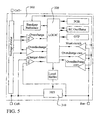
- Fig. 5 illustrates an exemplary application of the present invention.
- Fig. 6 illustrates the first preferred embodiment using a PMOS FET switch.
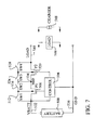
- Fig. 7 illustrates the second preferred embodiment using two PMOS FET switches.
-
- The preferred embodiments disclose a novel circuit for protecting a battery. The circuit uses a novel, single FET device having a switchable bulk connection to achieve control of both charging and discharging current. Additional switchable bulk FET devices may be cascaded to increase the operating range of the circuit. It should be clear to those experienced in the art that the present invention can be applied and extended without deviating from the scope of the present invention.
- Referring now to Fig. 2, the first preferred embodiment of the battery protection circuit of the present invention is illustrated. Several important features of the present invention are shown. A
battery 70 preferably comprises a rechargeable battery. The circuit is configured to allow thebattery 70 to source current to aload 88 or to be recharged by a chargingsource 90. Thebattery 70 preferably comprises a two-terminal device. In the illustration, the positive terminal is labeledVBATT 92. The negative terminal is labeledGND 96. - The battery protection circuit comprises, first, a
FET switch N1 78. In this version of the first preferred embodiment, a single FET switch and, more preferably, aNMOS FET switch 78 is used. An alternative version, showing a PMOS FET switch is shown as Fig. 6. Referring again to Fig. 2, theFET switch N1 78 is preferably fabricated in a standard MOS process such that thecontrol circuit 74 and theswitch N1 78 can be fabricated on the same substrate. As a particularly important feature, theNMOS FET N1 78 must be fabricated in a well (p-type) that can be isolated from the semiconductor substrate. In this way, the well, or bulk, of the device can be biased independently of the substrate. The NMOSFET switch N1 78 has gate, drain, source, and bulk connections. The source is coupled to the external load terminal GNDOUT 94 that is further coupled to an external device, such as a portable phone circuit or a chargingsource 90. The drain is coupled to the negativebattery terminal GND 96. The gate is coupled to thecontrol circuit 74. Thecontrol circuit 74 monitors thebattery 70 voltage, fromVBATT 92 toGND 96, to protect the battery from over charging and from over discharging. - A most important feature of the present invention is the configuration of the bulk connection of the
NMOS FET N1 78. Note that the bulk is not coupled to either the source or the drain as in the prior art. Further, the bulk is not coupled to any fixed voltage level. Rather, a switchable bulk is used. In particular, the bulk is switchable between thenegative battery terminal 96 and the load terminal GNDOUT 94. A first switch SW1 82 allows the bulk to be coupled to or de-coupled from thenegative battery terminal 96. A second switch SW2 86 allows the bulk to be coupled to or de-coupled from the load terminal GNDOUT 94. - These key structural features of the present invention are used to allow a single NMOS
FET switch N1 78 to perform the function of the two switches in the prior art. The operating table for the circuit is given in Table 1 below.Operating Conditions for Single NMOS FET Circuit. Operating Condition FET Condition Bulk Coupling Charging ON SW2 ON Over Charging OFF SW2 ON Charging in Over Discharge State MOS Diode SW2 ON Discharging ON SW1 ON Over Discharging OFF SW1 ON Discharging in Over Charge State MOS Diode SW1 ON - During a normal charging event, the NMOS
FET switch N1 78 is turned ON by thecontrol circuit 74. The bulk is coupled to the load terminal GNDOUT 94 by closing SW2 86 and opening SW1 82. With the bulk biased to GNDOUT, the gate drive of the control circuit can create a minimum ON resistance for NMOS switch N1. The chargingsource 90 can then source current into the battery to fully recharge it. However, if an over charging condition is detected, wherein the battery voltage rises above a pre-determined set point, then thecontrol circuit 74 turns OFF the NMOSFET switch N1 78 to stop charging current flow. Because the bulk is coupled to GNDOUT 94, a reverse biased p-n diode formed by the bulk and the drain prevents charging current flow from thenegative battery terminal 96 to GNDOUT 94. - In the normal discharging case, the NMOS
FET switch N1 78 is turned ON by thecontrol circuit 74. In this case, the bulk is coupled to the negativebattery terminal GND 96 by closing the switch SW1 82 while opening the switch SW2 86. Discharging current flows throughN1 78 from GNDOUT 94 toGND 96. If an over discharge occurs, the battery voltage will drop below a pre-determined value. During an over-discharge, the NMOSFET switch N1 78 is turned OFF by thecontrol circuit 74. However, the bulk remains coupled to thenegative terminal GND 96. The bulk-to-source diode is reverse biased and blocks any forward current flow. - Two other error conditions may occur. First, the battery may be charging during an over discharge state. In the over discharge state, the battery has been excessively discharged during a previous operation. During the subsequent charging, the charging current should be limited to protect the battery. Therefore, the gate of
N1 78 is coupled to thedrain node GND 96 such that the device operates as a MOS diode. In the second condition, the battery may be discharging in an overcharged stated. In this state, the battery has been overcharged. During the subsequent discharging, the current should again be limited to protect the battery. Therefore, the gate ofN1 78 is coupled to the source node GNDOUT 94 such that the device again operates as a MOS diode, in this case for forward current. - Referring now to Fig. 6, an alternative to the first preferred embodiment of the present invention is shown. In this embodiment, a PMOS FET is used for the
switch P1 408. In many processes, the NMOS transistor provides much lower ON resistance and is, therefore, the logical choice for a drive switch. However, if a suitable PMOS FET is available, the present invention is easily extendable to use a PMOS FET as the switch. In this case, thePMOS FET switch 408 has source coupled to theload terminal LOAD 428 and drain coupled to the positivebattery terminal VBATT 420. The gate is controlled by thecontrol circuit 404. The bulk is again switchable. In this case, however, the bulk is switched between thepositive battery terminal 420 andLOAD 428 by switches SW1 412 andSW2 416, respectively. Once again, the bulk of the PMOS device must be a well (n-type) that can be biased independently of the substrate. The operating table for the single PMOS FET version is shown as Table 2 below and operates as the NMOS FET version operates.Operating Conditions for Single PMOS FET Circuit. Operating Condition FET Condition Bulk Coupling Charging ON SW2 ON Over Charging OFF SW2 ON Charging in Over Discharge State MOS Diode SW2 ON Discharging ON SW1 ON Over Discharging OFF SW1 ON Discharging in Over Charge State MOS Diode SW1 ON - During a normal charging, the PMOS
FET switch P1 408 is ON while the bulk is biased to theoutput LOAD 428 by turningON SW2 416 and turningOFF SW1 412. This enables theswitch P1 408 to exhibit minimum ON resistance while not turning on the bulk-to-drain diode and risking latchup. If an over charging is detected, the PMOS FET is turned OFF while the bulk remains at LOAD. The current is thereby blocked by both the switching channel and the reverse biased p-n diode. During a normal discharge,P1 408 is ON while the bulk is biased to thepositive battery terminal 420 by turningON SW1 412 and turningOFF SW2 416. Again, this minimizes the ON resistance. During an over discharge, P1 is turned OFF and the bulk is left at VBATT to_insure no forward current. The charging during over discharge condition and the discharging during over charge conditions operate the same as for the NMOS case. - Referring now to Fig. 3, a second preferred embodiment of the present invention is illustrated. In this embodiment, two NMOS FET switches
N1 108 andN2 120 are used. N1 and N2 are cascaded to provide a combined switch having a larger operating voltage range than is available with a single switch. By nature, thebattery charging source 136 is capable of generating a larger voltage than thebattery 100. When an over charge condition is detected, and the single FET switch is turned OFF, the voltage difference between thecharger 90 and thebattery 70 must be sustained across the switch. Even with the novel switched bulk structure, the voltage range of the switch is limited by the drain-to-bulk reverse breakdown as given be the manufacturing process. This breakdown voltage may be about 7 Volts, for example. This means that thecharger 90 design must be limited to not generate a voltage greater than thebattery 70 voltage plus about 7 Volts. - Referring again to Fig. 3, the use of the cascaded NMOS
FET devices N1 108 andN2 120 increases the operating range of the combined switch such that a voltage difference of, for example, about 14 Volts can be sustained in the OFF state. The first FET switch N1 has gate, source, drain, and bulk. The drain is coupled to the negative battery terminal,GND 148. The bulk is switchably coupled between the negativebattery terminal GND 148 and amiddle node MID 142 between the cascadedFET devices N1 108 andN2 120. The secondFET switch N2 120 has gate, source, drain, and bulk. The drain is coupled to the first FET switch N1 drain at themid node MID 142. The source is coupled to the_loadterminal node GNDOUT 144. The bulk ofN2 120 is switchably coupled betweenMID 142 and theload terminal GNDOUT 144. The control circuit CONTROL 104 drives the gates ofN1 108 andN2 120 and the bulk switchesSW1 112,SW2 116,SW3 124, and SW4 128. The operating table for the second embodiment using cascaded NMOS FET switches is shown as Table 3 below.Operating modes for Cascaded NMOS Circuit. Mode N1 BULK N1 N2 BULK N2 Charging ON SW2 ON ON SW4 ON Over Charging OFF SW2 ON OFF SW4 ON Charging in Over Discharged State ON SW2 ON MOS DIODE SW4 ON Discharging ON SW1 ON ON SW3 ON Over Discharging ON SW1 ON OFF SW3 ON Discharging in Over Charged State ON SW1 ON MOS DIODE SW3 ON - The operating concept of the single NMOS FET is extended to create the cascaded switch. When the circuit is in the charging or discharging mode, both of the transistors N1 and N2 are ON. The bulk of
N1 108 is coupled to theMID node 142 by turningON SW2 116. The bulk ofN2 120 is coupled to theload terminal GNDOUT 144 by turning ON SW4 128. If an over charging condition is detected, the control circuit 104 turns OFF both switches N1 and N2 to interrupt current flow. The configuration of the bulks presents a series of reversed biased p-n junctions between the negativebattery terminal GND 148 and the load terminal GNDOUT to thereby block charging current. The use of two NMOS devices allows the voltage difference betweenGND 148 andGNDOUT 144 to drop across two bulk-to-drain diodes and thereby increases the operating range when compared to a single transistor approach. - If an over discharge event is detected, the control circuit 104 turns
OFF N2 120. In this case, however the bulk ofN1 108 is coupled toGND 148 bySW1 112 and the bulk ofN2 120 is coupled toMID 142 bySW3 124. This creates a series of reverse biased p-n diodes from theGNDOUT 144 toGND 148. Discharging current flow is thereby stopped by the channel of N2 and the reverse-biased diodes. - In the charging an over discharged battery case and in the discharging the over charged battery case, the cascaded circuit works in a similar mode as the single FET circuit. Note that the
first transistor N1 108 is held ON for both cases. However, thesecond transistor N2 120 is biased to the MOS diode case to protect the battery as in the single FET circuit. - Referring now to Fig. 7, a PMOS version of the second embodiment cascade circuit is shown. In the PMOS version, two PMOS FET switches
P1 508 andP2 520 are connected is series. The bulk for the firstPMOS FET P1 508 is switched between the positivebattery terminal VBATT 532 and theMID node 534. The bulk of the secondPMOS FET P2 520 is switched between theMID node 534 and theload terminal LOAD 540. The operating table for the PMOS version of the cascaded circuit is shown below in Table 4 and is the same as that for the cascaded NMOS version.Operating modes for Cascaded PMOS Circuit. Mode N1 BULK N1 N2 BULK N2 Charging ON SW2 ON ON SW4 ON Over Charging OFF SW2 ON OFF SW4 ON Charging in Over Discharged State ON SW2 ON MOS DIODE SW4 ON Discharging ON SW1 ON ON SW3 ON Over Discharging ON SW1 ON OFF SW3 ON Discharging in Over Charged State ON SW1 ON MOS DIODE SW3 ON - During normal charging mode, both
P1 508 andP2 520 are ON. The bulk of P1 is coupled toMID 534 while the bulk of P2 520 is coupled to LOAD 540 to minimize the ON resistance of the switches. If an over charge is detected, both P1 and P2 are turned OFF by thecontrol circuit 504. The bulk of P1 remains at MID while the bulk of P2 remains at LOAD. This creates a series of reverse biased p-n diodes betweenVBATT 532 and thehigh voltage LOAD 540 to block current flow into thebattery 500. During discharging, P1 and P2 are ON. The bulk of P1 is biased to VBATT while the bulk of P2 is biased to MID to reduce ON resistance. If an over discharge is detected, P2 is turned OFF. The bulk of P1 is kept atVBATT 532 while the bulk of P2 is kept atMID 534. This presents a series of reverse biased p-n diodes between VBATT and LOAD. - The cascaded switching configuration of the second embodiment, as illustrated in Figs. 3 and 7, may be extended to three or more switches if needed to create adequate operating voltage. A problem that the may occur with the cascaded switch configuration is the floating of the MID node when both of the FET switches are OFF. Referring again to Fig. 3, if an over charging event causes both
N1 108 andN2 120 to be switched OFF, then the bulk of N1 is coupled toMID 142 and the bulk of N2 is coupled toGNDOUT 144. Because the bulk-drain p-n diodes are reverse biased, the bulk of N1, which is coupled to MID, is actually floating. A non-uniform voltage distribution between the two bulk-drain diodes may exist and could cause one of the diodes to conduct. - Referring now to Fig. 4, this problem is eliminated by adding a
voltage divider Z 1 232 andZ 2 236 between the positivebattery terminal VBATT 248 and theload terminal GNDOUT 252. The purpose of the voltage divider is to provide a means of insuring that the voltage difference is evenly split between each bulk-drain diode so that the full operating range is achieved without turning on the parasitic vertical npn. Thevoltage divider Z 1 232 andZ 2 236 may comprise, for example, two resistors of equal value. The addition of the voltage divider to steer the bulk potentials may also be added to the PMOS version of the cascaded switch circuit shown in Fig. 7. In addition to thevoltage divider Z 1 232 andZ 2 236, switches SW5 and SW6 are added to allow the biasing voltage to be switched ON and OFF as needed. The operating table for third embodiment including the voltage divider is shown as Table 5 below. The voltage divider is only coupled to the MID node when the circuit is in the charging mode. Note that the same operating table applies to both NMOS and PMOS versions.Operating modes for Cascaded Circuit including Voltage Divider. Mode SW5 SW6 N1 BULK N1 N2 BULK N2 Charging ON OFF ON SW2 ON ON SW4 ON Over Charging ON ON OFF SW2 ON OFF SW4 ON Charging in Over Discharged State ON OFF ON SW2 ON MOS DIODE SW4 ON Discharging OFF OFF ON SW1 ON ON SW3 ON Over Discharging OFF OFF ON SW1 ON OFF SW3 ON Discharging in Over Charged State OFF OFF ON SW1 ON MOS DIODE SW3 ON - Referring now to Fig. 5, a block level diagram of an application of the present invention is shown. A battery control and
protection circuit 300 for a rechargeable battery is shown. Thecircuit 300 may comprise a single monolithic IC or a combination of IC chips and discrete components. Circuits are included to detect over voltage and current conditions. Thelogic block 320 uses these inputs to control the FET block 310 which comprises either a single FET or cascaded FET devices as disclosed in the present invention. - The present invention provides an effective and very manufacturable circuit for protecting a battery. The battery protection circuit controls charging and discharging of a battery. Both charging and discharging is controlled via a single FET having a switchable bulk connection. Switchable bulk FET devices may be cascaded to increase the voltage range of the circuit. The switchable bulk FET devices may comprise either NMOS or PMOS devices. The middle node between cascaded FET devices is steered to a known voltage during over charging to further improve performance.
- As shown in the preferred embodiments, the novel circuit provides an effective and manufacturable alternative to the prior art.
Claims (32)
- A battery charging, discharging, and protection circuit comprising:a FET switch having gate, source, drain, and bulk, wherein said source is coupled to a load terminal and said drain is coupled to a battery terminal anda means of controlling said FET switch gate and said bulk wherein said FET switch gate voltage determines the OFF and ON state of said FET switch and wherein said bulk is switchably coupled between said battery terminal and said load terminal.
- The circuit according to Claim 1 wherein said FET switch comprises a NMOS FET and said battery terminal comprises a negative battery terminal.
- The circuit according to Claim 1 wherein said FET switch comprises a PMOS FET and said battery terminal comprises a positive battery terminal.
- The circuit according to Claim 1 wherein said means of controlling and said FET switch comprise a single integrated circuit device.
- The circuit according to Claim 1 wherein said bulk is coupled to said load terminal during battery charging.
- The circuit according to Claim 5 wherein said FET switch is turned to said ON state during normal charging and is turned to said OFF state during over charging.
- The circuit according to Claim 5 wherein said FET switch acts as a MOS diode during charging in a battery over discharge state.
- The circuit according to Claim 1 wherein said bulk is coupled to said battery terminal during battery discharging.
- The circuit according to Claim 8 wherein said FET switch is turned to said ON state during normal discharging and is turned to said OFF state during over discharging.
- The circuit according to Claim 8 wherein said FET switch acts as a MOS diode during discharging in a battery over charge state.
- A battery charging, discharging, and protection circuit comprising:a first FET switch having gate, source, drain, and bulk, wherein said drain is coupled to a battery terminal;a second FET switch having gate, source, drain, and bulk, wherein said drain is coupled to said first NMOS FET switch source to thereby form a mid node and wherein said source is coupled to a load terminal; anda means of controlling said first and second FET gates and switchable bulks wherein said first and second FET switch gates voltages determine the OFF and ON states of said first and second FET switches, wherein said first FET bulk is switchably coupled between said battery terminal and said mid node, and wherein said second FET bulk is switchably coupled between said mid node and said load terminal.
- The circuit according to Claim 11 wherein said first and second FET switches comprise NMOS FET devices and wherein said battery terminal comprises a negative battery terminal.
- The circuit according to Claim 11 wherein said first and second FET switches comprise PMOS FET devices and wherein said battery terminal comprises a positive battery terminal.
- The circuit according to Claim 11 wherein said means of controlling and said FET switches comprise a single integrated circuit device.
- The circuit according to Claim 11 wherein said first FET switch bulk is coupled to said mid node and said second FET switch is coupled to said load terminal during battery charging.
- The circuit according to Claim 15 wherein said first FET switch and said second FET switch are turned to said ON state during normal charging and are turned to said OFF state during over charging.
- The circuit according to Claim 15 wherein said first FET switch is turned to said ON state and said second FET switch acts as a MOS diode during charging in a battery over discharge state.
- The circuit according to Claim 11 wherein said first FET switch bulk is coupled to said battery terminal and said second FET switch bulk is coupled to said mid node during battery discharging.
- The circuit according to Claim 18 wherein said first and second FET switches are turned to said ON state during normal discharging and wherein said second FET switch is turned to said OFF state during over discharging.
- The circuit according to Claim 18 wherein said first FET switch is turned to said ON state and said second FET switch acts as a MOS diode during discharging in a battery over charge state.
- The circuit according to Claim 11 further comprising:a voltage divider having an output comprising a voltage value between a second battery terminal voltage and said load terminal voltage; anda means of coupling said voltage divider output and said mid node.
- The circuit according to Claim 21 wherein said switch is turned ON during battery charging and said switch is turned OFF during battery discharging.
- A battery charging, discharging, and protection circuit comprising:a first FET switch having gate, source, drain, and bulk, wherein said drain is coupled to a first battery terminal;a second FET switch having gate, source, drain, and bulk, wherein said drain is coupled to said first NMOS FET switch source to thereby form a mid node and wherein said source is coupled to a load terminal;a voltage divider having an output comprising a voltage value between a second battery terminal voltage and said load terminal voltage;a means of coupling said voltage divider output and said mid node; anda means of controlling said first and second FET gates, said switchable bulks, and said switch wherein said first and second FET switch gates voltages determine the OFF and ON states of said first and second FET switches, wherein said first FET bulk is switchably coupled between said first battery terminal and said mid node, and wherein said second FET bulk is switchably coupled between said mid node and said load terminal.
- The circuit according to Claim 23 wherein said first and second FET switches comprise NMOS FET devices and wherein said first battery terminal comprises a negative battery terminal and said second battery terminal comprises a positive battery terminal.
- The circuit according to Claim 23 wherein said first and second FET switches comprise PMOS FET devices and wherein said first battery terminal comprises a positive battery terminal and said second battery terminal comprises a negative battery terminal.
- The circuit according to Claim 23 wherein said means of controlling and said FET switches comprise a single integrated circuit device.
- The circuit according to Claim 23 wherein said first FET switch bulk is coupled to said mid node, wherein said second FET switch bulk is coupled to said load terminal during battery charging, and wherein said voltage divider output is coupled to said mid node during battery charging.
- The circuit according to Claim 27 wherein said first FET switch and said second FET switch are turned to said ON state during normal charging and are turned to said OFF state during over charging.
- The circuit according to Claim 27 wherein said first FET switch is turned to said ON state and said second FET switch acts as a MOS diode during charging in a battery over discharge state.
- The circuit according to Claim 23 wherein said first FET switch bulk is coupled to said battery terminal, wherein said second FET switch bulk is coupled to said mid node, and wherein said voltage divider output is not coupled to said mid node during battery discharging.
- The circuit according to Claim 30 wherein said first and second FET switches are turned to said ON state during normal discharging and wherein said second FET switch is turned to said OFF state during over discharging.
- The circuit according to Claim 30 wherein said first FET switch is turned to said ON state and said second FET switch acts as a MOS diode during discharging in a battery over charge state.
Priority Applications (2)
| Application Number | Priority Date | Filing Date | Title |
|---|---|---|---|
| EP01480132A EP1320168A1 (en) | 2001-12-12 | 2001-12-12 | Power switch for battery protection |
| US10/017,601 US6670790B2 (en) | 2001-12-12 | 2001-12-14 | Power switch for battery protection |
Applications Claiming Priority (1)
| Application Number | Priority Date | Filing Date | Title |
|---|---|---|---|
| EP01480132A EP1320168A1 (en) | 2001-12-12 | 2001-12-12 | Power switch for battery protection |
Publications (1)
| Publication Number | Publication Date |
|---|---|
| EP1320168A1 true EP1320168A1 (en) | 2003-06-18 |
Family
ID=8183433
Family Applications (1)
| Application Number | Title | Priority Date | Filing Date |
|---|---|---|---|
| EP01480132A Withdrawn EP1320168A1 (en) | 2001-12-12 | 2001-12-12 | Power switch for battery protection |
Country Status (2)
| Country | Link |
|---|---|
| US (1) | US6670790B2 (en) |
| EP (1) | EP1320168A1 (en) |
Cited By (5)
| Publication number | Priority date | Publication date | Assignee | Title |
|---|---|---|---|---|
| WO2006135062A1 (en) * | 2005-06-17 | 2006-12-21 | Rohm Co., Ltd. | Semiconductor device, power supply device, and information processing device |
| EP2630714A4 (en) * | 2010-12-09 | 2013-12-04 | Csmc Technologies Fab1 Co Ltd | LITHIUM BATTERY PROTECTION CIRCUITS |
| CN103474967A (en) * | 2012-06-07 | 2013-12-25 | 苏州赛芯电子科技有限公司 | Highly-integrated battery protection circuit |
| CN107611936A (en) * | 2016-07-11 | 2018-01-19 | 三美电机株式会社 | Secondary battery protection circuit |
| CN109449891A (en) * | 2018-11-06 | 2019-03-08 | 苏州赛芯电子科技有限公司 | Improve the single-wafer battery protecting circuit and charge-discharge circuit of anti-peak voltage ability |
Families Citing this family (32)
| Publication number | Priority date | Publication date | Assignee | Title |
|---|---|---|---|---|
| DE10203512B4 (en) * | 2002-01-30 | 2021-09-02 | Robert Bosch Gmbh | Hand machine tool with an electric drive, a switching device and a battery unit |
| JP4150297B2 (en) * | 2003-06-30 | 2008-09-17 | ソニー株式会社 | Field effect transistor drive circuit |
| US20070097572A1 (en) * | 2005-10-28 | 2007-05-03 | Caretta Integrated Circuits | Protective circuit |
| US7626360B2 (en) * | 2006-08-11 | 2009-12-01 | Cirrus Logic, Inc. | Charge-pump biased battery protection circuit |
| JP5194412B2 (en) * | 2006-09-19 | 2013-05-08 | 株式会社リコー | Back gate voltage generation circuit, four-terminal back gate switching FET, charge / discharge protection circuit using the FET, battery pack incorporating the charge / discharge protection circuit, and electronic device using the battery pack |
| US7830120B2 (en) * | 2007-09-18 | 2010-11-09 | Nexergy, Inc. | Low side N-channel FET protection circuit |
| JP5130906B2 (en) * | 2007-12-26 | 2013-01-30 | サンケン電気株式会社 | Switch device |
| US8174209B2 (en) * | 2008-01-30 | 2012-05-08 | Texas Instruments Deutschland Gmbh | DC-DC converter and method for minimizing battery peak pulse loading |
| JP5193619B2 (en) * | 2008-01-31 | 2013-05-08 | 株式会社東芝 | Secondary battery system |
| US7999512B2 (en) * | 2008-12-16 | 2011-08-16 | Hong Kong Applied Science & Technology Research Institute Company, Ltd. | Single-power-transistor battery-charging circuit using voltage-boosted clock |
| EP2226937B1 (en) * | 2009-03-03 | 2012-02-08 | STMicroelectronics (Grenoble) SAS | Analog switch |
| US20110068735A1 (en) * | 2009-09-22 | 2011-03-24 | Texas Instruments Incorporated | Systems and Methods of Accurate Control of Battery Pre-charge Current |
| JP5504964B2 (en) * | 2010-02-22 | 2014-05-28 | ミツミ電機株式会社 | Protection monitoring circuit and battery pack |
| CN201789282U (en) * | 2010-05-21 | 2011-04-06 | 上海新进半导体制造有限公司 | Battery charge/discharge protection circuit |
| JP2012060762A (en) * | 2010-09-08 | 2012-03-22 | Seiko Instruments Inc | Charge and discharge control circuit, and battery device |
| JP5706648B2 (en) * | 2010-09-08 | 2015-04-22 | セイコーインスツル株式会社 | Charge / discharge control circuit and battery device |
| JP5706649B2 (en) * | 2010-09-08 | 2015-04-22 | セイコーインスツル株式会社 | Charge / discharge control circuit and battery device |
| US8471529B2 (en) * | 2010-10-14 | 2013-06-25 | GM Global Technology Operations LLC | Battery fault tolerant architecture for cell failure modes parallel bypass circuit |
| US8541981B2 (en) * | 2010-11-10 | 2013-09-24 | Texas Instruments Incorporated | Low-voltage dual-power-path management architecture for rechargeable battery monitoring solutions |
| US8675328B2 (en) | 2011-02-07 | 2014-03-18 | Aeroflex Plainview, Inc. | Battery charge protection system |
| US8519773B2 (en) | 2011-06-17 | 2013-08-27 | Texas Instruments Incorporated | Power switch with one-shot discharge and increased switching speed |
| EP2815482B1 (en) * | 2012-02-14 | 2018-05-16 | Nokia Technologies Oy | Method and circuitry for battery protection |
| US20130265010A1 (en) * | 2012-04-06 | 2013-10-10 | Semiconductor Energy Laboratory Co., Ltd. | Protective circuit module and battery pack |
| US8947156B2 (en) * | 2012-11-09 | 2015-02-03 | Fairchild Semiconductor Corporation | High-voltage bulk driver using bypass circuit |
| CN104348225B (en) * | 2014-08-12 | 2017-07-11 | 矽力杰半导体技术(杭州)有限公司 | A kind of battery charge-discharge circuit of Single switch and the control method of battery charging and discharging |
| TWI531134B (en) * | 2014-12-29 | 2016-04-21 | 廣達電腦股份有限公司 | Battery power unit |
| KR101830281B1 (en) * | 2015-08-20 | 2018-02-20 | 주식회사 아이티엠반도체 | Battery protection circuit module and battery pack including the same |
| WO2017030321A1 (en) * | 2015-08-20 | 2017-02-23 | 주식회사 아이티엠반도체 | Battery protection circuit module and battery pack comprising same |
| JP6577916B2 (en) * | 2016-07-11 | 2019-09-18 | ミツミ電機株式会社 | Protection IC |
| EP3361596B1 (en) * | 2017-02-08 | 2020-04-29 | VARTA Microbattery GmbH | Battery with a battery management system which comprises an electronic switching circuit |
| TWI692175B (en) * | 2019-06-27 | 2020-04-21 | 宏碁股份有限公司 | Power control circuit and power control method |
| CN111146515B (en) * | 2019-12-23 | 2021-02-26 | 电子科技大学 | Chip cascade circuit based on diode realization |
Citations (5)
| Publication number | Priority date | Publication date | Assignee | Title |
|---|---|---|---|---|
| EP0720270A2 (en) * | 1994-12-30 | 1996-07-03 | SILICONIX Incorporated | Low-side bidirectional battery disconnect switch |
| US5933046A (en) * | 1995-09-05 | 1999-08-03 | Stmicroelectronics, S.A. | Low-voltage analog switch having selective bulk biasing circuitry |
| US6087807A (en) * | 1992-11-24 | 2000-07-11 | Seiko Instruments Inc. | Charge/discharge control circuit and chargeable electric power source apparatus |
| WO2000059093A1 (en) * | 1999-03-27 | 2000-10-05 | Koninklijke Philips Electronics N.V. | Switch circuit and semiconductor switch, for battery-powered equipment |
| JP2001177387A (en) * | 1999-12-17 | 2001-06-29 | Nissan Motor Co Ltd | Load drive |
Family Cites Families (5)
| Publication number | Priority date | Publication date | Assignee | Title |
|---|---|---|---|---|
| KR890005226B1 (en) | 1986-12-29 | 1989-12-18 | 삼성반도체통신 주식회사 | Battery protection circuit |
| US5081371A (en) | 1990-11-07 | 1992-01-14 | U.S. Philips Corp. | Integrated charge pump circuit with back bias voltage reduction |
| US5789900A (en) * | 1994-12-05 | 1998-08-04 | Fuji Photo Film Co., Ltd. | Device for protecting a secondary battery from overcharge and overdischarge |
| US6160381A (en) | 1998-05-21 | 2000-12-12 | Qualcomm Inc. | Battery pack protection circuit and battery pack including a protection circuit |
| US6246214B1 (en) | 2000-05-10 | 2001-06-12 | Motorola, Inc. | Multiple use of a single transistor for linear regulation charge control and protection of a rechargeable battery |
-
2001
- 2001-12-12 EP EP01480132A patent/EP1320168A1/en not_active Withdrawn
- 2001-12-14 US US10/017,601 patent/US6670790B2/en not_active Expired - Lifetime
Patent Citations (5)
| Publication number | Priority date | Publication date | Assignee | Title |
|---|---|---|---|---|
| US6087807A (en) * | 1992-11-24 | 2000-07-11 | Seiko Instruments Inc. | Charge/discharge control circuit and chargeable electric power source apparatus |
| EP0720270A2 (en) * | 1994-12-30 | 1996-07-03 | SILICONIX Incorporated | Low-side bidirectional battery disconnect switch |
| US5933046A (en) * | 1995-09-05 | 1999-08-03 | Stmicroelectronics, S.A. | Low-voltage analog switch having selective bulk biasing circuitry |
| WO2000059093A1 (en) * | 1999-03-27 | 2000-10-05 | Koninklijke Philips Electronics N.V. | Switch circuit and semiconductor switch, for battery-powered equipment |
| JP2001177387A (en) * | 1999-12-17 | 2001-06-29 | Nissan Motor Co Ltd | Load drive |
Non-Patent Citations (1)
| Title |
|---|
| PATENT ABSTRACTS OF JAPAN vol. 2000, no. 23 10 February 2001 (2001-02-10) * |
Cited By (7)
| Publication number | Priority date | Publication date | Assignee | Title |
|---|---|---|---|---|
| WO2006135062A1 (en) * | 2005-06-17 | 2006-12-21 | Rohm Co., Ltd. | Semiconductor device, power supply device, and information processing device |
| JP5057973B2 (en) * | 2005-06-17 | 2012-10-24 | ローム株式会社 | Semiconductor device, power supply device, information processing device |
| EP2630714A4 (en) * | 2010-12-09 | 2013-12-04 | Csmc Technologies Fab1 Co Ltd | LITHIUM BATTERY PROTECTION CIRCUITS |
| CN103474967A (en) * | 2012-06-07 | 2013-12-25 | 苏州赛芯电子科技有限公司 | Highly-integrated battery protection circuit |
| CN107611936A (en) * | 2016-07-11 | 2018-01-19 | 三美电机株式会社 | Secondary battery protection circuit |
| CN107611936B (en) * | 2016-07-11 | 2019-06-07 | 三美电机株式会社 | Secondary battery protection circuit |
| CN109449891A (en) * | 2018-11-06 | 2019-03-08 | 苏州赛芯电子科技有限公司 | Improve the single-wafer battery protecting circuit and charge-discharge circuit of anti-peak voltage ability |
Also Published As
| Publication number | Publication date |
|---|---|
| US20030122525A1 (en) | 2003-07-03 |
| US6670790B2 (en) | 2003-12-30 |
Similar Documents
| Publication | Publication Date | Title |
|---|---|---|
| US6670790B2 (en) | Power switch for battery protection | |
| US7030591B2 (en) | Integrated circuit implementing protection switch for battery charging and discharging with enhanced reverse voltage protection | |
| JP7277775B2 (en) | Secondary battery protection circuit, secondary battery protection device, battery pack, and control method for secondary battery protection circuit | |
| KR100352401B1 (en) | Charge/discharge control circuit and chargeable electric power source apparatus | |
| JP4844468B2 (en) | Secondary battery protection device and semiconductor integrated circuit device | |
| US10283981B2 (en) | Protection IC and semiconductor integrated circuit | |
| KR101642789B1 (en) | Integrated circuit apparatus for secondary battery protection, secondary battery protection module using the same and battery pack | |
| US20070210759A1 (en) | Charge/discharge protection circuit and power-supply unit | |
| JP2012222865A (en) | Battery protection circuit and battery protection device, and battery pack | |
| JPH07131938A (en) | Charge / discharge control circuit and rechargeable power supply | |
| CN100495727C (en) | Switching element and protection circuit using the same | |
| US7403363B2 (en) | Switching element and protection circuit using the same | |
| JP2000102182A (en) | Overcharge / overdischarge prevention circuit for secondary battery | |
| CN1307796C (en) | Driving circuit for field effect transistor | |
| EP1339154A1 (en) | Monolithic battery protection circuit | |
| KR20050057693A (en) | Charge-discharge protect circuit | |
| JPH11103528A (en) | Charge / discharge protection circuit and battery pack | |
| US20230411972A1 (en) | Driving circuit applied to protection switch of battery module | |
| TW202135418A (en) | Charge and discharge control circuit and battery device | |
| KR20210048851A (en) | Battery disconnect apparatus and battery apparatus including the same | |
| JP2001251771A (en) | Rechargeable battery or rechargeable battery pack, electronic device having any of these | |
| JP3197698B2 (en) | Battery charge / discharge circuit |
Legal Events
| Date | Code | Title | Description |
|---|---|---|---|
| PUAI | Public reference made under article 153(3) epc to a published international application that has entered the european phase |
Free format text: ORIGINAL CODE: 0009012 |
|
| AK | Designated contracting states |
Designated state(s): AT BE CH CY DE DK ES FI FR GB GR IE IT LI LU MC NL PT SE TR |
|
| AX | Request for extension of the european patent |
Extension state: AL LT LV MK RO SI |
|
| 17P | Request for examination filed |
Effective date: 20031217 |
|
| AKX | Designation fees paid |
Designated state(s): AT BE CH CY DE DK ES FI FR GB GR IE IT LI LU MC NL PT SE TR |
|
| STAA | Information on the status of an ep patent application or granted ep patent |
Free format text: STATUS: THE APPLICATION IS DEEMED TO BE WITHDRAWN |
|
| 18D | Application deemed to be withdrawn |
Effective date: 20060701 |