EP1317062A2 - Steuerung der Stromversorgung von kaskadierten Verstärkern in einer Sendeschaltung - Google Patents
Steuerung der Stromversorgung von kaskadierten Verstärkern in einer Sendeschaltung Download PDFInfo
- Publication number
- EP1317062A2 EP1317062A2 EP02257920A EP02257920A EP1317062A2 EP 1317062 A2 EP1317062 A2 EP 1317062A2 EP 02257920 A EP02257920 A EP 02257920A EP 02257920 A EP02257920 A EP 02257920A EP 1317062 A2 EP1317062 A2 EP 1317062A2
- Authority
- EP
- European Patent Office
- Prior art keywords
- power supply
- transmission
- opening
- amplifier
- power
- Prior art date
- Legal status (The legal status is an assumption and is not a legal conclusion. Google has not performed a legal analysis and makes no representation as to the accuracy of the status listed.)
- Withdrawn
Links
Images

Classifications
-
- H—ELECTRICITY
- H03—ELECTRONIC CIRCUITRY
- H03F—AMPLIFIERS
- H03F3/00—Amplifiers with only discharge tubes or only semiconductor devices as amplifying elements
- H03F3/72—Gated amplifiers, i.e. amplifiers which are rendered operative or inoperative by means of a control signal
-
- H—ELECTRICITY
- H03—ELECTRONIC CIRCUITRY
- H03F—AMPLIFIERS
- H03F3/00—Amplifiers with only discharge tubes or only semiconductor devices as amplifying elements
- H03F3/20—Power amplifiers, e.g. Class B amplifiers, Class C amplifiers
- H03F3/24—Power amplifiers, e.g. Class B amplifiers, Class C amplifiers of transmitter output stages
-
- H—ELECTRICITY
- H04—ELECTRIC COMMUNICATION TECHNIQUE
- H04B—TRANSMISSION
- H04B1/00—Details of transmission systems, not covered by a single one of groups H04B3/00 - H04B13/00; Details of transmission systems not characterised by the medium used for transmission
- H04B1/38—Transceivers, i.e. devices in which transmitter and receiver form a structural unit and in which at least one part is used for functions of transmitting and receiving
- H04B1/40—Circuits
- H04B1/44—Transmit/receive switching
-
- H—ELECTRICITY
- H03—ELECTRONIC CIRCUITRY
- H03F—AMPLIFIERS
- H03F2203/00—Indexing scheme relating to amplifiers with only discharge tubes or only semiconductor devices as amplifying elements covered by H03F3/00
- H03F2203/72—Indexing scheme relating to gated amplifiers, i.e. amplifiers which are rendered operative or inoperative by means of a control signal
- H03F2203/7206—Indexing scheme relating to gated amplifiers, i.e. amplifiers which are rendered operative or inoperative by means of a control signal the gated amplifier being switched on or off by a switch in the bias circuit of the amplifier controlling a bias voltage in the amplifier
-
- H—ELECTRICITY
- H04—ELECTRIC COMMUNICATION TECHNIQUE
- H04B—TRANSMISSION
- H04B1/00—Details of transmission systems, not covered by a single one of groups H04B3/00 - H04B13/00; Details of transmission systems not characterised by the medium used for transmission
- H04B1/02—Transmitters
- H04B1/04—Circuits
- H04B2001/0408—Circuits with power amplifiers
Definitions
- the present invention relates to a transmission circuit for a transmitter/receiver for use in a cordless telephone set.
- a power amplifier 51 includes three stages of amplifiers 51a, 51b, and 51c in a cascade connection, the first stage amplifier 51a and the second stage amplifier 51b each have a gain of 14 dB, and the final stage, third stage amplifier 51c has a gain of 14 dB.
- the output end of the third stage amplifier 51c is connected with an impedance matching circuit 52 including a strip line 52a and a capacitor 52b.
- the power amplifier 51 is connected through the impedance matching circuit 52 with an antenna that is not shown.
- the first stage amplifier 51a is provided with a transmission signal about at 0 dBm as an input.
- the power amplifier 51 is supplied with power supply voltage from transmission/reception switch means 53.
- the transmission/reception switch means 53 includes an NPN transistor 53a and a PNP transistor 53b.
- the NPN transistor 53a has its emitter grounded and its collector connected to the base of the PNP transistor 53b through a resistor 53c.
- the PNP transistor 53b has its emitter connected to a power supply B and its base connected to the power supply B through a resistor 53d.
- the collector that supplies the power amplifier 51 with power supply voltage is connected with the power supply end of the first stage amplifier 51a through a series feeding circuit 54 including a resistor 54a and a strip line 54b.
- the strip line 54b has a length substantially 1/4 of the wavelength of the transmission signal.
- the connection node of the resistor 54a and the strip line 54b is grounded through a grounding capacitor 55 to deal with high frequencies.
- the PNP transistor 53b has its collector directly connected to the power supply end of the second stage amplifier 51b, and also to the output end of the impedance matching circuit 52 through a feeding strip line 56. It is also connected to the output end of the third stage amplifier 51c through a strip line 52a. The output end also serves as a power supply end.
- the feeding strip line 56 also has a length substantially 1/4 of the wavelength of the transmission signal.
- the connection node of the collector of the PNP transistor 53b and the feeding strip line 56 is grounded through a grounding capacitor 57 to deal with high frequencies.
- a transmission/reception switch signal T/R to turn on/off the NPN transistor 53a is input to the base of the transistor.
- the transmission/reception switch signal T/R attains a high level. This turns on the NPN transistor 53a and the PNP transistor 53b, so that power supply voltage is supplied to the amplifiers 51a, 51b, and 51c.
- the transmission signal input to the first stage amplifier 51a is amplified by the amplifiers 51a, 51b, and 51c, and output to the antenna through the impedance matching circuit 52.
- the output power is about 28 dBm.
- the impedance in view of the power supply side from the output end of the impedance matching circuit 52 is high, so that the transmission signal output from the third stage amplifier 51c is not leaked to the power supply side through the feeding strip line 56.
- the transmission/reception switch signal T/R attains a low level. This turns off the NPN transistor 53a and the PNP transistor 53b, so that the power supply voltage supplied to the amplifiers 51a, 51b, and 51c is interrupted.
- the power output at the conventional transmission circuit is substantially fixed at a level of 28 dBm, and therefore more than necessary power is output for example when a base unit and a sub unit transmit/receive a signal in close proximity to each other. Therefore, in the power amplifier, especially in the final stage amplifier, excess current is wasted. In addition, since the output power is so large that other electronic equipment used at home could be interfered with.
- the transmission signal is not leaked onto the feeding strip line. Meanwhile, if the length varies, the impedance in view of the feeding strip line is lowered and the transmission signal is leaked. As a result, not only the transmission power is lowered but also current by the leaked signal is passed to a position where the grounding capacitor is grounded. At the time, when another circuit is formed near the grounding position, the ground potential of the circuit fluctuates, which makes the operation of the circuit unstable. Particularly when a PLL circuit is the other circuit, the oscillation frequency fluctuates.
- Another object of the invention is to restrain transmission signal current coming onto a feeding strip line that supplies power supply voltage to the output end of a power amplifier when the length of the feeding strip line varies from a length substantially 1/4 of the wavelength of the transmission signal.
- a transmission circuit comprising a power amplifier including a plurality of amplifiers in a cascade connection, and transmission/reception switch means for supplying the power amplifier with power supply voltage in a transmission mode, and interrupting the power supply voltage supplied to the power amplifier in a reception mode.
- the transmission/reception switch means can interrupt only the power supply voltage supplied to the final stage amplifier in the power amplifier in the transmission mode.
- the transmission/reception switch means may include first opening/closing means for supplying an amplifier other than the final stage amplifier with the power supply voltage, second opening/closing means for supplying the final stage amplifier with the power supply voltage, control means for controlling the opening/closing operation of the first and second opening/closing means, and third opening/closing means interposed between the control means and the second opening/closing means, and the third switch means can be opened/closed.
- the first opening/closing means may include a first PNP transistor having its emitter connected to the power supply for supplying voltage from its collector to an amplifier other than the final stage amplifier, the second opening/closing means includes a second PNP transistor having its emitter connected to the power supply for supplying voltage from its collector to the final stage amplifier, the control means includes an NPN transistor having its emitter grounded and its collector connected to the power supply and the base of the first PNP transistor through a resistor, the third opening/closing means includes a single gate FET having its source connected to the collector of the NPN transistor and its drain connected to the power supply and the base of the second PNP transistor through a resistor, a transmission/reception switch signal to turn on/off the NPN transistor is input to the base of the NPN transistor, and a transmission power switch signal to turn on/off the single gate FET is input to the gate of the single gate FET.
- a transmission circuit comprising a power amplifier having an output end serving as a power supply end, and a feeding strip line substantially as long as 1/4 of the wavelength of a transmission signal that supplies the power supply end with voltage from a power supply.
- the power supply side end in the feeding strip line is grounded through a terminating circuit including a grounding capacitor that attains a low impedance at the frequency of a transmission signal and a resistor connected in series to the grounding capacitor, so that the resistance value of the resistor is set to a value that can be ignored with respect to the characteristic impedance of the feeding strip line.
- the resistance value of the resistor may be in the range from 2 Q to 10 Q.
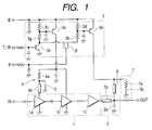
- a transmission circuit according to the invention will be described in conjunction with Fig. 1.
- a power amplifier 1 includes three stages of amplifiers 1a, 1b, and 1c in a cascade connection, and the first stage amplifier 1a and the second stage amplifier 1b each have a gain of about 7 dB, while the final stage, third stage amplifier 1c has a gain of about 14 dB.
- a transmission signal at a level of about 0 dBm is input to the first stage amplifier 1a.
- the output end of the third stage amplifier 1c is connected with an impedance matching circuit 2 including a strip line 2a and a capacitor 2b.
- the power amplifier 1 is connected through the impedance matching circuit 2 with an antenna that is not shown.
- the power amplifier 1 is supplied with power supply voltage from transmission/reception switch means 3.
- the transmission/reception switch means 3 includes a first PNP transistor 3a as first opening/closing means, and a second PNP transistor 3b as second opening/closing means.
- the first PNP transistor 3a has its emitter connected to a power supply B and its base connected to the power supply B through a resistor 3c.
- the second PNP transistor 3b has its emitter connected to the power supply B and its base connected to the power supply B through a resistor 3d.
- the transmission/reception switch means 3 further includes an NPN transistor 3e serving as control means to carry out control to turn on/off both the first and second PNP transistors 3a and 3b, and a single gate FET 3f serving as third opening/closing means.
- the NPN transistor 3e has its emitter grounded and its collector connected to the base of the first PNP transistor 3a through a resistor 3g.
- the single gate FET 3f has its source connected to the collector of the NPN transistor 3e, and its drain connected to the base of the second PNP transistor 3b through a resistor 3h.
- a transmission/reception switch signal T/R to turn on/off the NPN transistor 3e to switch between the transmission and reception modes is input to the base of the transistor.
- a transmission power switch signal P to turn on/off the single gate FET 3f is input to the gate of the single gate.
- the transmission power switch signal P is input from a reception circuit that is not shown. When for example a base unit and a sub unit transmit/receive a signal in close proximity to each other, the received signal level is high. Therefore, the single gate FET is turned off when the level is equal to or higher than a prescribed value.
- the first PNP transistor 3a has its collector connected to the power supply end of the first stage amplifier 1a through the series feeding circuit 4 including a resistor 4a and a strip line 4b.
- the strip line 4b has a length substantially 1/4 of the wavelength of a transmission signal.
- the connection node of the resistor 4a and the strip line 4b is grounded through a grounding capacitor 5 to deal with high frequencies.
- the first PNP transistor 3a has its collector directly connected to the power supply end of the second stage amplifier 1b.
- the second PNP transistor 3b has its collector connected to the output end of the impedance matching circuit 2 through a feeding strip line 6, from which the output end of the third stage amplifier 1c is supplied with voltage.
- the output end of the third stage amplifier 1c serves as a power supply end.
- the feeding strip line 6 also has a length substantially 1/4 of the wavelength of the transmission signal.
- the connection node of the collector of the second PNP transistor 3b and the feeding strip line 6 (one end on the power supply side) is grounded through a series terminating circuit 7 including a resistor 7a and a grounding capacitor 7b whose high frequency impedance is extremely low.
- the resistance value of the resistor 7a is set to a value about in the range from 2 ⁇ to 10 Q that can be ignored with respect to the characteristic impedance of the feeding strip line 6.
- the transmission/reception switch signal T/R attains a high level. This turns on the NPN transistor 3e and the first PNP transistor 3a. Then, voltage is supplied to the first stage amplifier 3a and the second stage amplifier 3b.
- the transmission power switch signal P attains a high level and the single gate FET 3f is turned on. This turns on the second PNP transistor 3b accordingly. Therefore, the third stage amplifier 3c is supplied with power supply voltage, so that a transmission signal at about 28 dBm is output from the power amplifier 1.
- the transmission power switch signal P attains a low level, and while the first PNP transistor 3a is still on, the second PNP transistor 3b is turned off. Then, only the voltage supplied to the third amplifier 3c is interrupted. As a result, in the power amplifier 1, the first stage amplifier 1a and the second stage amplifier 1b operate, while the third stage amplifier 1c does not operate.
- the third amplifier 1c serves as an attenuator for about 14 dBm and therefore the level of the signal at 14 dBm output from the second stage amplifier 1b becomes substantially 0 dBm. Current of about 100 mA (milliamperes) otherwise supplied to the third stage amplifier 1c is saved.
- the transmission/reception switch signal T/R attains a low level, and the NPN transistor 3f is turned off. This turns off the first PNP transistor 3b and the second PNP transistor 3b is turned off regardless of the on/off state of the single gate FET 3f. Therefore, the power supply voltage supplied to the amplifiers 1a, 1b, and 1c is interrupted.
- a power amplifier including a plurality of amplifiers in a cascade connection, and transmission/reception switch means for supplying the power amplifier with power supply voltage in a transmission mode, and interrupting the power supply voltage supplied to the power amplifier in a reception mode.
- the transmission/reception switch means can interrupt only the power supply voltage supplied to the final stage amplifier in the power amplifier in the transmission mode. Therefore, when the power supply to the final stage amplifier is interrupted at the time of transmission to a base station in close proximity, communication with the base station can be maintained with reduced transmission power. Therefore, the power consumption can be reduced, and the interference with other electronic equipment can be eliminated.
- the transmission/reception switch means includes first opening/closing means for supplying an amplifier other than the final stage amplifier with the power supply voltage, second opening/closing means for supplying the final stage amplifier with the power supply voltage, control means for controlling the opening/closing operation of the first and second opening/closing means, and third opening/closing means interposed between the control means and the second opening/closing means, and the third switch means can be opened/closed. Therefore, only the power supply voltage supplied to the final stage amplifier can be interrupted.
- a transmission/reception switch signal to turn on/off the NPN transistor as the control means is input to the base of the transistor, and a transmission power switch signal to turn on/off the single gate FET is input to the gate of the single gate FET. Therefore, the first and second PNP transistors that feed the amplifiers can be turned on by the NPN transistor when the single gate FET is on, so that only the second PNP transistor that feeds the final stage amplifier can be turned off by the single gate FET in this state.
- a power amplifier having an output end serving as a power supply end, and a feeding strip line substantially as long as 1/4 of the wavelength of a transmission signal that supplies the power supply end with voltage from a power supply, and the power supply side end in the feeding strip line is grounded through a terminating circuit including a grounding capacitor that attains a low impedance at the frequency of a transmission signal and a resistor connected in series with the grounding capacitor, so that the resistance value of the resistor is set to a value that can be ignored with respect to the characteristic impedance of the feeding strip line. Therefore, when the length of the feeding strip line varies from substantially the 1/4 length, a transmission signal coming onto the feeding strip line can be restrained. Therefore, potential fluctuations in the grounded position of the terminating circuit can be reduced.
- the resistance value of the resistor is set in the range from 2 ⁇ to 10 ⁇ . Therefore, the impedance in view of the feeding strip line side can be kept at a high level.
Landscapes
- Engineering & Computer Science (AREA)
- Power Engineering (AREA)
- Computer Networks & Wireless Communication (AREA)
- Signal Processing (AREA)
- Amplifiers (AREA)
- Transmitters (AREA)
Applications Claiming Priority (4)
| Application Number | Priority Date | Filing Date | Title |
|---|---|---|---|
| JP2001351556 | 2001-11-16 | ||
| JP2001351556A JP2003152465A (ja) | 2001-11-16 | 2001-11-16 | 送信回路 |
| JP2001351557A JP2003152466A (ja) | 2001-11-16 | 2001-11-16 | 送信回路 |
| JP2001351557 | 2001-11-16 |
Publications (2)
| Publication Number | Publication Date |
|---|---|
| EP1317062A2 true EP1317062A2 (de) | 2003-06-04 |
| EP1317062A3 EP1317062A3 (de) | 2003-10-01 |
Family
ID=26624565
Family Applications (1)
| Application Number | Title | Priority Date | Filing Date |
|---|---|---|---|
| EP02257920A Withdrawn EP1317062A3 (de) | 2001-11-16 | 2002-11-15 | Steuerung der Stromversorgung von kaskadierten Verstärkern in einer Sendeschaltung |
Country Status (1)
| Country | Link |
|---|---|
| EP (1) | EP1317062A3 (de) |
Cited By (1)
| Publication number | Priority date | Publication date | Assignee | Title |
|---|---|---|---|---|
| GB2463702A (en) * | 2008-09-23 | 2010-03-24 | Technetix Group Ltd | An amplifier system for cable television network which has a power delay device |
Citations (4)
| Publication number | Priority date | Publication date | Assignee | Title |
|---|---|---|---|---|
| JPS6239908A (ja) * | 1985-08-14 | 1987-02-20 | Mitsubishi Electric Corp | バイアス回路 |
| JPH0377401A (ja) * | 1989-08-19 | 1991-04-03 | Fujitsu Ltd | マイクロ波集積回路装置 |
| US5661434A (en) * | 1995-05-12 | 1997-08-26 | Fujitsu Compound Semiconductor, Inc. | High efficiency multiple power level amplifier circuit |
| WO1999031799A1 (en) * | 1997-12-16 | 1999-06-24 | Samsung Electronics Co., Ltd. | Power saving device for radio communication terminal |
-
2002
- 2002-11-15 EP EP02257920A patent/EP1317062A3/de not_active Withdrawn
Patent Citations (4)
| Publication number | Priority date | Publication date | Assignee | Title |
|---|---|---|---|---|
| JPS6239908A (ja) * | 1985-08-14 | 1987-02-20 | Mitsubishi Electric Corp | バイアス回路 |
| JPH0377401A (ja) * | 1989-08-19 | 1991-04-03 | Fujitsu Ltd | マイクロ波集積回路装置 |
| US5661434A (en) * | 1995-05-12 | 1997-08-26 | Fujitsu Compound Semiconductor, Inc. | High efficiency multiple power level amplifier circuit |
| WO1999031799A1 (en) * | 1997-12-16 | 1999-06-24 | Samsung Electronics Co., Ltd. | Power saving device for radio communication terminal |
Non-Patent Citations (2)
| Title |
|---|
| PATENT ABSTRACTS OF JAPAN vol. 011, no. 220 (E-524), 16 July 1987 (1987-07-16) & JP 62 039908 A (MITSUBISHI ELECTRIC CORP), 20 February 1987 (1987-02-20) * |
| PATENT ABSTRACTS OF JAPAN vol. 015, no. 246 (E-1081), 24 June 1991 (1991-06-24) & JP 03 077401 A (FUJITSU LTD), 3 April 1991 (1991-04-03) * |
Cited By (1)
| Publication number | Priority date | Publication date | Assignee | Title |
|---|---|---|---|---|
| GB2463702A (en) * | 2008-09-23 | 2010-03-24 | Technetix Group Ltd | An amplifier system for cable television network which has a power delay device |
Also Published As
| Publication number | Publication date |
|---|---|
| EP1317062A3 (de) | 2003-10-01 |
Similar Documents
| Publication | Publication Date | Title |
|---|---|---|
| EP0700169B1 (de) | Sende-/Empfangsumschaltes für Radiokommunikationsgerät | |
| US6118989A (en) | High frequency variable gain amplifier device and wireless communications terminal | |
| US5724004A (en) | Voltage bias and temperature compensation circuit for radio frequency power amplifier | |
| US5589796A (en) | Method and apparatus for increasing amplifier efficiency | |
| US20060009164A1 (en) | Radio frequency switching circuit | |
| EP0818879B1 (de) | Verstärkerschaltung und mehrstufige Verstärkerschaltung | |
| JPH07143056A (ja) | 移動体通信装置 | |
| JPH11317690A (ja) | ラジオトランシ―バ用受信機直線性の適応制御技術 | |
| US6624700B2 (en) | Radio frequency power amplifier for cellular telephones | |
| KR20030017650A (ko) | 송수신기 및 무선 주파수 송수신기 모듈 및 송수신기를구비한 장치 | |
| US6025753A (en) | Method and apparatus for amplifying a signal | |
| JP3107035B2 (ja) | 低雑音増幅器及びその制御回路 | |
| EP0622895B1 (de) | Kommunikationsapparat mit Leistungsverstärker | |
| JP3238931B2 (ja) | デジタル携帯電話器 | |
| KR100300451B1 (ko) | 온도보상레벨시프터를구비한전력증폭기회로 | |
| US5193217A (en) | Low voltage IC for voice operated transceiver | |
| EP1317062A2 (de) | Steuerung der Stromversorgung von kaskadierten Verstärkern in einer Sendeschaltung | |
| EP1387485B1 (de) | Schaltung für leistungsverstärker | |
| US5805986A (en) | High-frequency step attenuator suitable for transmission circuit | |
| US6594478B1 (en) | Self oscillating mixer | |
| US6518843B1 (en) | Variable gain type amplifier | |
| JP2003152465A (ja) | 送信回路 | |
| JP2003152466A (ja) | 送信回路 | |
| JP2000323944A (ja) | 高周波利得可変増幅器 | |
| JP2002171177A (ja) | 中間周波数がゼロである構造の送信機で、htb技術によるパワー増幅器を使用可能にする制御方法および回路 |
Legal Events
| Date | Code | Title | Description |
|---|---|---|---|
| PUAI | Public reference made under article 153(3) epc to a published international application that has entered the european phase |
Free format text: ORIGINAL CODE: 0009012 |
|
| AK | Designated contracting states |
Designated state(s): AT BE BG CH CY CZ DE DK EE ES FI FR GB GR IE IT LI LU MC NL PT SE SK TR |
|
| AX | Request for extension of the european patent |
Extension state: AL LT LV MK RO SI |
|
| PUAL | Search report despatched |
Free format text: ORIGINAL CODE: 0009013 |
|
| RIC1 | Information provided on ipc code assigned before grant |
Ipc: 7H 03F 3/19 B Ipc: 7H 04B 1/44 B Ipc: 7H 03G 3/30 B Ipc: 7H 04B 7/005 B Ipc: 7H 03F 1/02 A |
|
| AK | Designated contracting states |
Kind code of ref document: A3 Designated state(s): AT BE BG CH CY CZ DE DK EE ES FI FR GB GR IE IT LI LU MC NL PT SE SK TR |
|
| AX | Request for extension of the european patent |
Extension state: AL LT LV MK RO SI |
|
| 17P | Request for examination filed |
Effective date: 20031024 |
|
| AKX | Designation fees paid |
Designated state(s): DE FR GB |
|
| 17Q | First examination report despatched |
Effective date: 20071004 |
|
| STAA | Information on the status of an ep patent application or granted ep patent |
Free format text: STATUS: THE APPLICATION IS DEEMED TO BE WITHDRAWN |
|
| 18D | Application deemed to be withdrawn |
Effective date: 20120601 |