EP1314209B1 - Method for producing a radiation-emitting semiconductor chip based on iii-v nitride semiconductor material, and a corresponding radiation-emitting semiconductor chip - Google Patents
Method for producing a radiation-emitting semiconductor chip based on iii-v nitride semiconductor material, and a corresponding radiation-emitting semiconductor chip Download PDFInfo
- Publication number
- EP1314209B1 EP1314209B1 EP01967062A EP01967062A EP1314209B1 EP 1314209 B1 EP1314209 B1 EP 1314209B1 EP 01967062 A EP01967062 A EP 01967062A EP 01967062 A EP01967062 A EP 01967062A EP 1314209 B1 EP1314209 B1 EP 1314209B1
- Authority
- EP
- European Patent Office
- Prior art keywords
- layer
- thin
- substrate
- film element
- growth
- Prior art date
- Legal status (The legal status is an assumption and is not a legal conclusion. Google has not performed a legal analysis and makes no representation as to the accuracy of the status listed.)
- Expired - Lifetime
Links
Images
Classifications
-
- B—PERFORMING OPERATIONS; TRANSPORTING
- B82—NANOTECHNOLOGY
- B82Y—SPECIFIC USES OR APPLICATIONS OF NANOSTRUCTURES; MEASUREMENT OR ANALYSIS OF NANOSTRUCTURES; MANUFACTURE OR TREATMENT OF NANOSTRUCTURES
- B82Y20/00—Nanooptics, e.g. quantum optics or photonic crystals
-
- H—ELECTRICITY
- H01—ELECTRIC ELEMENTS
- H01L—SEMICONDUCTOR DEVICES NOT COVERED BY CLASS H10
- H01L33/00—Semiconductor devices with at least one potential-jump barrier or surface barrier specially adapted for light emission; Processes or apparatus specially adapted for the manufacture or treatment thereof or of parts thereof; Details thereof
- H01L33/005—Processes
- H01L33/0062—Processes for devices with an active region comprising only III-V compounds
- H01L33/0066—Processes for devices with an active region comprising only III-V compounds with a substrate not being a III-V compound
- H01L33/007—Processes for devices with an active region comprising only III-V compounds with a substrate not being a III-V compound comprising nitride compounds
-
- H—ELECTRICITY
- H01—ELECTRIC ELEMENTS
- H01L—SEMICONDUCTOR DEVICES NOT COVERED BY CLASS H10
- H01L33/00—Semiconductor devices with at least one potential-jump barrier or surface barrier specially adapted for light emission; Processes or apparatus specially adapted for the manufacture or treatment thereof or of parts thereof; Details thereof
- H01L33/005—Processes
- H01L33/0062—Processes for devices with an active region comprising only III-V compounds
- H01L33/0075—Processes for devices with an active region comprising only III-V compounds comprising nitride compounds
-
- H—ELECTRICITY
- H01—ELECTRIC ELEMENTS
- H01L—SEMICONDUCTOR DEVICES NOT COVERED BY CLASS H10
- H01L33/00—Semiconductor devices with at least one potential-jump barrier or surface barrier specially adapted for light emission; Processes or apparatus specially adapted for the manufacture or treatment thereof or of parts thereof; Details thereof
- H01L33/005—Processes
- H01L33/0093—Wafer bonding; Removal of the growth substrate
-
- H—ELECTRICITY
- H01—ELECTRIC ELEMENTS
- H01S—DEVICES USING THE PROCESS OF LIGHT AMPLIFICATION BY STIMULATED EMISSION OF RADIATION [LASER] TO AMPLIFY OR GENERATE LIGHT; DEVICES USING STIMULATED EMISSION OF ELECTROMAGNETIC RADIATION IN WAVE RANGES OTHER THAN OPTICAL
- H01S5/00—Semiconductor lasers
- H01S5/30—Structure or shape of the active region; Materials used for the active region
- H01S5/34—Structure or shape of the active region; Materials used for the active region comprising quantum well or superlattice structures, e.g. single quantum well [SQW] lasers, multiple quantum well [MQW] lasers or graded index separate confinement heterostructure [GRINSCH] lasers
- H01S5/343—Structure or shape of the active region; Materials used for the active region comprising quantum well or superlattice structures, e.g. single quantum well [SQW] lasers, multiple quantum well [MQW] lasers or graded index separate confinement heterostructure [GRINSCH] lasers in AIIIBV compounds, e.g. AlGaAs-laser, InP-based laser
- H01S5/34333—Structure or shape of the active region; Materials used for the active region comprising quantum well or superlattice structures, e.g. single quantum well [SQW] lasers, multiple quantum well [MQW] lasers or graded index separate confinement heterostructure [GRINSCH] lasers in AIIIBV compounds, e.g. AlGaAs-laser, InP-based laser with a well layer based on Ga(In)N or Ga(In)P, e.g. blue laser
Definitions
- the invention relates to a method for producing a radiation-emitting semiconductor chip based on III-V nitride semiconductor material according to the preamble of patent claim 1 and to a radiation-emitting semiconductor chip according to the preamble of patent claim 19.
- GaN-based radiation-emitting semiconductor components are, for example, made US 5,874,747 known.
- Such semiconductor devices include a semiconductor body having a plurality of layers made of GaN or a material based thereon. According to the cited document, the plurality of GaN-based layers are applied to a SiC substrate.
- III-V nitride semiconductor materials include the materials derived from GaN or materials related to GaN and, for example, ternary or quaternary mixed crystals based thereon.
- these include the materials AlN, InN, AlGaN (Al 1-x Ga x N, 0 ⁇ x ⁇ 1), InGaN (In 1-x Ga x N, 0 ⁇ x ⁇ 1), InAlN (In 1-x Al x N, 0 ⁇ x ⁇ 1) and AlInGaN (Al 1-xy In x Ga y N, 0 ⁇ x ⁇ 1, 0 ⁇ y ⁇ 1).
- III-V nitride semiconductor material refers to the group of materials described above. Furthermore, this term includes materials used to form buffer layers in the epitaxial fabrication of layers of the recited material systems.
- GaN-based semiconductor bodies having an intermediate SiC substrate formed on the original epitaxial substrate are known.
- the original substrate body is removed during manufacture.
- SiC substrates themselves are extremely expensive. If parts of the SiC substrate are incorporated in a semiconductor component with each semiconductor body based on III-V nitride semiconductor materials, the costs for the semiconductor component are directly linked to the costs of the SiC substrate. A cost-effective production of the semiconductor device is made difficult.
- SiC substrate in semiconductor chips based on III-V nitride semiconductors can lead to a reduction in the radiation yield, since SiC partially absorbs the radiation emitted by these and thus reduces the proportion of coupled-out radiation.
- These thin substrates are required to prevent cracking in the semiconductor body due to the different thermal expansion coefficients between silicon and III-V nitride semiconductor based materials.
- the radiation-emitting semiconductor chip based on III-V nitride semiconductor material is formed as a thin-film element.
- a thin-film element is understood as meaning a semiconductor layer sequence which consists essentially exclusively of a stack of epitaxial layers based on III-V nitride semiconductor material.
- the thin-film element consists of a plurality of III-V nitride semiconductor epitaxial layers, wherein the semiconductor body is bounded on one side by an n-conducting and on the opposite side by a p-type epitaxial layer.
- the thin-film element is applied with the p-type side on a conductive support having a mounting surface has for the thin-film element and preferably at the same time can be used for contacting the thin-film element.
- contact surface refers to this contact surface without further details.
- the semiconductor chip thus formed no epitaxial substrate usual thickness (> 100 microns), such as a SiC substrate, so that the material costs are lowered for the semiconductor device.
- a further advantage of the thin-film embodiment is that the semiconductor body contains only small residues of a radiation-absorbing substrate or no radiation-absorbing substrate.
- the radiation efficiency can be increased by using a reflective carrier.
- An advantageous development of the invention consists in forming the thin film element on the n-type side limiting epitaxial layer as a conductive buffer layer.
- buffer layers in the fabrication of GaN-based semiconductor bodies is common to compensate for lattice mismatch between the epitaxial substrate and the epitaxial layers following the buffer layer.
- a conductive buffer layer has the great advantage that a vertically conductive semiconductor device can be created with the semiconductor body thus formed.
- the buffer layer is formed in multiple layers.
- the buffer layer is formed in multiple layers.
- the buffer layer consists of AlGaN-based materials, such as Al 1-x Ga x N where 0 ⁇ x ⁇ 1 and Al 1-xy In x Ga y N where 0 ⁇ x ⁇ 1, 0 ⁇ y ⁇ 1 and x + y ⁇ 1.
- the surface finish and the crystalline quality of such low Al content layers are low, it is advantageous to form the contact surface side remote from the high Al content buffer layer.
- the high Al content increases the surface quality of the buffer layer and achieves good adaptation to subsequent III-V nitride semiconductor-based layers.
- a buffer layer with a low Al content on the side of the contact surface and high Al content on the opposite side thus advantageously forms a conductive buffer layer with a high surface quality at the same time.
- the III-V nitride semiconductor-based layers are applied to an epitaxial substrate, the substrate body of which is matched to a III-V nitride semiconductor material or one in comparison to III-V nitride semiconductor materials.
- Nitride semiconductor materials has greater thermal expansion coefficient and that is limited on the epitaxial side of a thin growth layer containing Si (111).
- the thermal expansion of the epitaxial substrate in the production of the III-V nitride semiconductor body is determined by the substrate body, so that the substrate behaves thermally similar to the layers to be applied.
- a Si (111) surface has a hexagonal structure and is thus well suited as an epitaxial surface for III-V nitride semiconductor materials.
- Si (111) surfaces are easy to process and prepare for epitaxy.
- the processing techniques of Si (111) are well known and proven in the semiconductor industry because of the superior use of this material.
- Polycrystalline SiC (PolySiC), GaN or polycrystalline GaN (PolyGaN) is preferably used as the substrate body the good thermal adaptation to GaN-based layers used.
- the substrate body may include sapphire ( ⁇ -Al 2 O 3 ), which has a larger thermal expansion coefficient than III-V nitride semiconductor materials.
- substrate bodies are significantly less expensive than the substrates used according to the prior art, since the semiconductor body is deposited on the surface of the growth layer and thus advantageously the requirements for the crystalline properties of the substrate body are reduced. Due to the reduced requirements in particular inexpensive polycrystalline materials can be used.
- the substrate body is preferably connected to the growth layer by an adhesive layer consisting of silicon oxide or silicon nitride.
- the method is continued after the application of the III-V nitride semiconductor-based layers by applying a carrier to the III-V nitride semiconductor-based layers in a next step.
- the epitaxial substrate is peeled off from the III-V nitride semiconductor-based layers.
- the use of an Si (111) growth layer as the epitaxial surface is advantageous in detaching the epitaxial substrate, since the semiconductor body can easily be detached from the substrate body, for example by etching.
- the Si (111) growth layer represents a sacrificial layer.
- a contact surface is applied after the epitaxial substrate has been detached from the surface of the semiconductor body from which the epitaxial substrate has been detached.
- An advantageous embodiment of the production method according to the invention consists in structuring the majority of the III-V nitride semiconductor layers prior to the detachment of the epitaxial substrate.
- structuring is to be understood as meaning measures which laterally subdivide the epitaxial layers into a multiplicity of individual epitaxial layer stacks arranged side by side on the epitaxial substrate.
- the structuring advantageously brings about an enlargement of the surface exposed to the etching attack.
- an intermediate carrier is first applied to the epitaxial layers based on III-V nitride semiconductor material. Thereafter, in turn, the epitaxial substrate peeled off and a support applied to the side of the epitaxial layers, from which the epitaxial substrate was peeled off. In the next step, the intermediate carrier is replaced.
- the layer sequence of the layers based on III-V nitride semiconductor material with respect to the carrier is advantageously reversed compared to the production method described above.
- This reversal is advantageous in order to be able to also use subsequent methods, in particular in the case of the housing, which require this reverse layer sequence.
- a particularly preferred embodiment of the production method according to the invention consists in applying as the first layer to the epitaxial substrate an electrically conductive buffer layer.
- Such a buffer layer is of particular advantage in order to produce for the following epitaxial layers a surface with optimally adapted lattice structure, which is at the same time well wetted by the subsequent layer materials and thus enables a uniform growth of the subsequent layers.
- the buffer layer is preferably formed from a plurality of individual layers based on AlGaN.
- a high Al buffer layer forms a lattice matched and well wettable surface for other III-V nitride semiconductor based layers, but has low conductivity, while a low Al content buffer layer conducts electricity well, but has lower crystalline quality and surface finish.
- the buffer layer is formed in two steps.
- a plurality of electrically conductive regions are applied to the growth layer of the epitaxial substrate.
- an InGaN-based material such as In 1-x Ga x N where 0 ⁇ x ⁇ 1 and In 1-xy Al x Ga y N where 0 ⁇ x ⁇ 1, 0 ⁇ y ⁇ is suitable as a material for the conductive regions 1 and x + y ⁇ 1, or GaN.
- this plurality of electrically conductive regions is covered with a planarizing filling layer, wherein the interstices between the conductive regions are filled.
- the material suitable for this is particularly an AlGaN compound with a high Al content.
- the buffer layer thus prepared is very well suited for the deposition of further Layers based on III-V nitride semiconductor material and has a high conductivity.
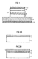
- the in FIG. 1 illustrated radiation-emitting semiconductor chip has a semiconductor body 11 in the form of a thin-film element, which consists of a conductive buffer layer 9 and a layer sequence 8, which contains in particular epitaxial layers based on III-V compound semiconductor material.
- a contact surface 12 is applied, which, unlike in Figure 1, can cover only a portion of the top of the semiconductor body 11 and, for example, have Al or may consist of Al and is designed as a bonding pad.
- the structure of the layer sequence 8 determines the functionality of the semiconductor body 11 or of the chip formed therewith. This layer sequence 8 also includes the radiation generation active layer.
- the semiconductor body 11 has no epitaxial substrate.
- the semiconductor body 11 is n-type and p-type on the opposite side.
- the semiconductor body 11 is deposited on a main surface of a conductive carrier 5.
- the carrier 5 has a second contact surface 10 on the side facing away from the semiconductor body 11.
- the semiconductor chip thus formed vertically, that is perpendicular to the layer planes, consistently conductive. This allows a lateral largely homogeneous current flow through the device and a simple contact.
- lateral scaling is meant the transition to other lateral dimensions of the chip. This transition is easily possible since the chip is not structured in the lateral direction, ie has no topology.
- a conductive buffer layer 9 is a prerequisite for a vertically conductive chip. This layer is formed, for example, from two layers of III-V nitride semiconductor materials. The more detailed nature of the buffer layer 9, together with the preparation of a conductive buffer layer based on FIG. 3 explained.
- the semiconductor bodies formed according to the invention are particularly suitable for realizing light-emitting diode chips with a central wavelength in the yellow, green, green-blue or violet spectral range, light-emitting diodes with particularly high luminosity and for realizing semiconductor lasers an emission wavelength in the green to violet spectral range.
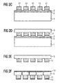
- FIG. 2 is schematically illustrated in six intermediate steps a to f an embodiment of a manufacturing method according to the invention.
- the starting point is a multilayer epitaxial substrate 100 (FIG. FIG. 2a ).
- the substrate body 1 is made of SiC, preferably Polysic.
- an adhesive layer 3 preferably consisting of silicon oxide is formed, which connects the substrate body with a thin growth layer 2, which consists for example of Si (111).
- the thickness of the growth layer 2 is chosen so small that its thermal expansion is essentially determined by the underlying substrate body 1.
- the thickness of the growth layer 2 is between about 0.1 .mu.m and 20 .mu.m, preferably it is less than 10 .mu.m and particularly preferably it is between 0.1 .mu.m and 2 .mu.m.
- a plurality of layers 4 of III-V nitride semiconductor materials are deposited, FIG. 2b ,
- a conductive AlGaN buffer layer 9 is preferably first formed on the surface of the growth layer 2, since GaN itself and InGaN compounds only poorly wet Si (111) or SiC surfaces.
- the buffer layer 9 and the adjacent layers based thereon on the basis of III-V compound semiconductor material are formed n-type.
- the epitaxial layer stack is bounded by one or more p-type layers.
- n-type and p-type layers Between the n-type and p-type layers, a plurality of Al 1-xy Ga x In y N-based layers having 0 ⁇ x ⁇ 1, 0 ⁇ x ⁇ 1 and x + y ⁇ 1 are formed, and the radiation generation is narrower Serve the purpose. Suitable for this purpose are all radiation-generating semiconductor structures known to the person skilled in the art, in particular pn junctions with the formation of a single or double heterostructure as well as single and multiple quantum well structures.
- the Al 1-xy Ga x In y N-based layers are laterally structured in the next step, Figure 2c , so that from these a plurality of separate, on the epitaxial substrate 100 juxtaposed layer stack is formed.
- These layer stacks essentially represent the not yet separated thin-film elements 11 of the radiation-emitting chips.
- the mesa etching takes place into the growth layer 2 of the epitaxial substrate 100 in order to take place in a following Step to allow easy detachment of the thin-film elements 11 of the epitaxial substrate 100.
- a carrier 5 or alternatively an intermediate carrier 13 is applied on the p-conducting side of the thin-film elements 11 remote from the epitaxy substrate 100.
- a carrier material for example, GaAs or Cu can be used.
- the epitaxial substrate 100 is detached from the thin-film element 11.
- the detachment is wet chemical by etching, wherein the growth layer 2 is destroyed.
- the wet chemical detachment with etching of the growth layer 2 requires a much lower cost than, for example, the replacement of a SiC substrate body.
- a carrier 5 is applied using an intermediate carrier 13 after the detachment of the epitaxial substrate 100 in its place, and then the intermediate carrier 13 is removed.
- the buffer layer 9 lies on the side of the semiconductor body facing the carrier 5 ( FIG. 2e , right). In the other case, the buffer layer 9 is formed on the side facing away from the carrier 5 of the semiconductor body 11.
- the semiconductor body 11 and the carrier 5 are provided with contact surfaces 12 and 10, respectively. Subsequently, the carrier 5 is severed between each of the semiconductor bodies 11, so that a plurality of in FIG. 1 illustrated semiconductor chips is formed ( FIG. 2f ).
- the bonding of the thin-film elements 11 to the carrier 5 or the intermediate carrier 13 in conjunction with the subsequent detachment of the epitaxial substrate 100 advantageously allows a further use of the epitaxial substrate body 1, resulting in a significant cost reduction in the case of SiC as a substrate body material.
- the entire substrate can be etched away if its reuse does not provide a particular advantage.
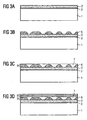
- FIG. 3 schematically illustrates the preparation of a conductive buffer layer 9 with reference to four intermediate steps.
- a SiC or PolySiC substrate body 1 having an epitaxial growth layer 2 containing, for example, Si (III) is used ( FIG. 3a ).
- a nucleation layer 6 in the form of a plurality of quantum dots is deposited ( FIG. 3b ).
- the material used for this is AlGaInN with a low Al content ( ⁇ 50%), InGaN or GaN.
- the quantum dots are highly conductive but do not form a closed layer. Thus arises on the surface of the growth layer, a plurality of mutually non-contiguous, electrically conductive areas. The degree of coverage can vary between 1% and 99% depending on the material composition.
- a planarizing AlGaN-based filling layer 7 with a high Al content for example Al x Ga 1-x N with x> 0.5 ( Figure 3c ) so that a planar structure 9 results.
- the conductive regions 6 form channel-like connections through the buffer layer 9 and ensure good electrical conductivity of the buffer layer 9.
- a layer sequence 8 which in particular contains epitaxial layers based on III-V compound semiconductor material, is deposited on the buffer layer 9 ( Figure 3c ), which essentially determines the functionality of the semiconductor device.
- compositions of the semiconductor materials can be adapted to the requirements and the intended use of the device in the specified frame.
- the central wavelength of the generated radiation can be determined.
Description
Die Erfindung bezieht sich auf ein Verfahren zum Herstellen eines strahlungsemittierenden Halbleiterchips auf Basis von III-V-Nitridhalbleitermaterial nach dem Oberbegriff des Patentanspruchs 1 sowie auf einen strahlungsemittierenden Halbleiterchip nach dem Oberbegriff des Patentanspruchs 19.The invention relates to a method for producing a radiation-emitting semiconductor chip based on III-V nitride semiconductor material according to the preamble of patent claim 1 and to a radiation-emitting semiconductor chip according to the preamble of patent claim 19.
Strahlungsemittierende Halbleiterbauelemente auf GaN-Basis sind beispielsweise aus
Unter III-V-Nitridhalbleitermaterialien fallen im vorliegenden Zusammenhang die von GaN abgeleiteten oder mit GaN verwandten Materialien sowie darauf aufbauende, beispielsweise ternäre oder quaternäre Mischkristalle. Insbesondere fallen hierunter die Materialien AlN, InN, AlGaN (Al1-xGaxN, 0≤x≤1), InGaN (In1-xGaxN, 0≤x≤1), InAlN (In1-xAlxN, 0≤x≤1) und AlInGaN (Al1-x-yInxGayN, 0≤x≤1, 0≤y≤1).In the present context, III-V nitride semiconductor materials include the materials derived from GaN or materials related to GaN and, for example, ternary or quaternary mixed crystals based thereon. In particular, these include the materials AlN, InN, AlGaN (Al 1-x Ga x N, 0≤x≤1), InGaN (In 1-x Ga x N, 0≤x≤1), InAlN (In 1-x Al x N, 0≤x≤1) and AlInGaN (Al 1-xy In x Ga y N, 0≤x≤1, 0≤y≤1).
Im folgenden bezieht sich die Bezeichnung "III-V-Nitridhalbleitermaterial" auf die oben beschriebene Gruppe von Materialien. Weiterhin umfaßt diese Bezeichnung Materialien, die zur Ausbildung von Pufferschichten bei der epitaktischen Herstellung von Schichten der angeführten Materialsysteme verwendet werden.In the following, the term "III-V nitride semiconductor material" refers to the group of materials described above. Furthermore, this term includes materials used to form buffer layers in the epitaxial fabrication of layers of the recited material systems.
Aus
Weiterhin ist aus
Aus
Die Verwendung von Halbleiterkörpern, die ein SiC-Substrat enthalten, bedeutet für die Herstellung von Halbleiterbauelementen einen zusätzlichen, nicht unerheblichen Kostenaufwand, da SiC-Substrate selbst extrem kostenaufwendig sind. Werden mit jedem auf III-V-Nitridhalbleitermaterialien basierenden Halbleiterkörper Teile des SiC-Substrats in ein Halbleiterbauelement eingebaut, so sind die Kosten für das Halbleiterbauelement direkt an die Kosten des SiC-Substrats gebunden. Eine kostengünstige Herstellung des Halbleiterbauelements wird dadurch erschwert.The use of semiconductor bodies containing a SiC substrate means an additional, not inconsiderable expense for the production of semiconductor devices, since SiC substrates themselves are extremely expensive. If parts of the SiC substrate are incorporated in a semiconductor component with each semiconductor body based on III-V nitride semiconductor materials, the costs for the semiconductor component are directly linked to the costs of the SiC substrate. A cost-effective production of the semiconductor device is made difficult.
Weiterhin kann ein SiC-Substrat in auf III-V-Nitridhalbleiter basierenden Halbleiterchips zur Verringerung der Strahlungsausbeute führen, da SiC die von diesen emittierte Strahlung teilweise absorbiert und somit den Anteil auskoppelbarer Strahlung reduziert.Furthermore, a SiC substrate in semiconductor chips based on III-V nitride semiconductors can lead to a reduction in the radiation yield, since SiC partially absorbs the radiation emitted by these and thus reduces the proportion of coupled-out radiation.
Bei dem in
Diese dünnen Substrate sind erforderlich, um Rißbildung im Halbleiterkörper aufgrund der verschiedenen thermischen Ausdehnungskoeffizienten zwischen Silizium und auf III-V-Nitridhalbleiter basierenden Materialien zu vermeiden.These thin substrates are required to prevent cracking in the semiconductor body due to the different thermal expansion coefficients between silicon and III-V nitride semiconductor based materials.
Es ist Aufgabe der vorliegenden Erfindung, einen strahlungsemittierenden Halbleiterchip auf Basis von III-V-Nitridhalbleitermaterialien technisch einfach und daher kostengünstig herzustellen, wobei der Halbleiterchip eine hohe externe Quanteneffizienz aufweist.It is the object of the present invention to produce a radiation-emitting semiconductor chip based on III-V nitride semiconductor materials in a technically simple and therefore cost-effective manner, the semiconductor chip having a high external quantum efficiency.
Diese Aufgabe wird durch ein Verfahren nach Anspruch 1 gelöst. Vorteilhafte Weiterbildungen der Erfindung sind Gegenstand der Unteransprüche.This object is achieved by a method according to claim 1. Advantageous developments of the invention are the subject of the dependent claims.
Erfindungsgemäß ist vorgesehen, den strahlungsemittierenden Halbleiterchip auf III-V-Nitridhalbleitermaterial-Basis als Dünnschichtelement auszubilden.According to the invention, the radiation-emitting semiconductor chip based on III-V nitride semiconductor material is formed as a thin-film element.
Unter einem Dünnschichtelement wird dabei eine Halbleiterschichtfolge verstanden, die im wesentlichen ausschließlich aus einem Stapel Epitaxieschichten auf der Basis von III-V-Nitridhalbleitermaterial besteht.In this case, a thin-film element is understood as meaning a semiconductor layer sequence which consists essentially exclusively of a stack of epitaxial layers based on III-V nitride semiconductor material.
Das Dünnschichtelement besteht aus einer Mehrzahl von III-V-Nitridhalbleiter-Epitaxieschichten, wobei der Halbleiterkörper auf einer Seite durch eine n-leitende und auf der dieser gegenüberliegenden Seite durch eine p-leitende Epitaxieschicht begrenzt ist.The thin-film element consists of a plurality of III-V nitride semiconductor epitaxial layers, wherein the semiconductor body is bounded on one side by an n-conducting and on the opposite side by a p-type epitaxial layer.
Das Dünnschichtelement ist mit der p-leitenden Seite auf einem leitfähigen Träger aufgebracht, der eine Montagefläche für das Dünnschichtelement aufweist und vorzugweise zugleich zur Kontaktierung des Dünnschichtelements verwendet werden kann.The thin-film element is applied with the p-type side on a conductive support having a mounting surface has for the thin-film element and preferably at the same time can be used for contacting the thin-film element.
Auf der n-leitenden Seite des Dünnschichtelements ist eine korrespondierende Kontaktfläche gebildet. Im folgenden bezieht sich die Bezeichnung "Kontaktfläche" ohne weitere Angaben auf diese Kontaktfläche.On the n-conductive side of the thin-film element, a corresponding contact surface is formed. In the following, the term "contact surface" refers to this contact surface without further details.
Mit großem Vorteil weist der so gebildete Halbleiterchip kein Epitaxiesubstrat üblicher Dicke (>100µm) wie zum Beispiel ein SiC-Substrat auf, so daß die Materialkosten für das Halbleiterbauelement gesenkt sind.With great advantage, the semiconductor chip thus formed no epitaxial substrate usual thickness (> 100 microns), such as a SiC substrate, so that the material costs are lowered for the semiconductor device.
Ein weiterer Vorteil der Dünnschichtausführung liegt darin, daß der Halbleiterkörper nur mehr kleine Reste eines strahlungsabsorbierenden Substrats oder gar kein strahlungsabsorbierendes Substrat enthält.A further advantage of the thin-film embodiment is that the semiconductor body contains only small residues of a radiation-absorbing substrate or no radiation-absorbing substrate.
Daher kann die Strahlungsausbeute durch Verwendung eines reflektierenden Trägers gesteigert werden.Therefore, the radiation efficiency can be increased by using a reflective carrier.
Eine vorteilhafte Weiterbildung der Erfindung besteht darin, bei dem Dünnschichtelement die auf der n-leitenden Seite begrenzende Epitaxieschicht als leitfähige Pufferschicht auszubilden.An advantageous development of the invention consists in forming the thin film element on the n-type side limiting epitaxial layer as a conductive buffer layer.
Die Ausbildung von Pufferschichten bei der Herstellung von GaN-basierenden Halbleiterkörpern ist üblich, um eine Gitterfehlanpassung zwischen Epitaxiesubstrat und den auf die Pufferschicht folgenden Epitaxieschichten auszugleichen.The formation of buffer layers in the fabrication of GaN-based semiconductor bodies is common to compensate for lattice mismatch between the epitaxial substrate and the epitaxial layers following the buffer layer.
Eine leitfähige Pufferschicht bringt den großen Vorteil mit sich, daß mit dem so gebildeten Halbleiterkörper ein vertikal leitfähiges Halbleiterbauelement geschaffen werden kann.A conductive buffer layer has the great advantage that a vertically conductive semiconductor device can be created with the semiconductor body thus formed.
Gegenüber isolierenden Pufferschichten ist dies vorteilhaft, da vertikal leitende Halbleiterchips mit geringerem Aufwand kontaktiert werden können. Ferner ist so eine größere laterale Ausdehnung der aktiven Schichten möglich.This is advantageous over insulating buffer layers since vertically conductive semiconductor chips can be contacted with less effort. Furthermore, a larger lateral extent of the active layers is possible.
Bei einer besonders bevorzugten Ausgestaltung der Erfindung ist die Pufferschicht mehrlagig gebildet. Durch eine Abfolge mehrerer Schichten unterschiedlicher Zusammensetzung ist es mit Vorteil möglich, sowohl die Leitfähigkeit der Pufferschicht als auch die Anpassung an die folgenden GaN-basierenden Schichten zu optimieren.In a particularly preferred embodiment of the invention, the buffer layer is formed in multiple layers. By a sequence of several layers of different composition, it is advantageously possible to optimize both the conductivity of the buffer layer and the adaptation to the following GaN-based layers.
Bei einer bevorzugten Ausgestaltung der Erfindung besteht die Pufferschicht aus AlGaN-basierenden Materialien, wie beispielsweise Al1-xGaxN mit 0≤x<1und Al1-x-yInxGayN mit 0≤x<1, 0≤y<1 und x+y<1.In a preferred embodiment of the invention, the buffer layer consists of AlGaN-based materials, such as Al 1-x Ga x N where 0≤x <1 and Al 1-xy In x Ga y N where 0≤x <1, 0≤y < 1 and x + y <1.
Von besonderem Vorteil ist es hierbei, die der Kontaktfläche zugewandte Seite der Pufferschicht mit niedrigem Al-Gehalt auszubilden, um so eine gut leitfähige Pufferschicht zu erhalten.It is particularly advantageous in this case to form the contact surface facing side of the buffer layer with low Al content, so as to obtain a highly conductive buffer layer.
Da die Oberflächengüte und die kristalline Qualität solcher Schichten mit niedrigem Al-Gehalt gering ist, ist es weiterhin vorteilhaft, die der Kontaktfläche abgewandte Seite der Pufferschicht mit hohem Al-Gehalt auszubilden. Durch den hohen Al-Gehalt wird die Oberflächengüte der Pufferschicht erhöht und eine gute Anpassung an nachfolgende III-V-Nitridhalbleiter-basierende Schichten erreicht.Further, since the surface finish and the crystalline quality of such low Al content layers are low, it is advantageous to form the contact surface side remote from the high Al content buffer layer. The high Al content increases the surface quality of the buffer layer and achieves good adaptation to subsequent III-V nitride semiconductor-based layers.
Eine Pufferschicht mit niedrigem Al-Gehalt auf der Seite der Kontaktfläche und hohem Al-Gehalt auf der gegenüberliegenden Seite bildet damit mit großem Vorteil eine leitfähige Pufferschicht mit zugleich hoher Oberflächengüte.A buffer layer with a low Al content on the side of the contact surface and high Al content on the opposite side thus advantageously forms a conductive buffer layer with a high surface quality at the same time.
Erfindungsgemäß ist zur Herstellung eines strahlungsemittierenden Halbleiterelements auf Basis von III-V-Nitridhalbleitermaterial vorgesehen, die III-V-Nitridhalbleiter-basierenden Schichten auf ein Epitaxiesubstrat aufzubringen, dessen Substratkörper einen an III-V-Nitridhalbleitermaterialien angepaßten oder einen im Vergleich zu III-V-Nitridhalbleitermaterialien größeren thermischen Ausdehnungskoeffizienten besitzt und das auf der Epitaxieseite von einer dünnen Aufwachsschicht, die Si(111) enthält, begrenzt wird.According to the invention, for the production of a radiation-emitting semiconductor element based on III-V nitride semiconductor material, the III-V nitride semiconductor-based layers are applied to an epitaxial substrate, the substrate body of which is matched to a III-V nitride semiconductor material or one in comparison to III-V nitride semiconductor materials. Nitride semiconductor materials has greater thermal expansion coefficient and that is limited on the epitaxial side of a thin growth layer containing Si (111).
Mit Vorteil wird so die thermische Ausdehnung des Epitaxiesubstrats bei der Herstellung des III-V-Nitridhalbleiterkörpers durch den Substratkörper bestimmt, so daß sich das Substrat thermisch ähnlich wie die aufzubringenden Schichten verhält.Advantageously, the thermal expansion of the epitaxial substrate in the production of the III-V nitride semiconductor body is determined by the substrate body, so that the substrate behaves thermally similar to the layers to be applied.
Eine Si(111)-Oberfläche weist eine hexagonale Struktur auf und ist damit gut als Epitaxieoberfläche für III-V-Nitridhalbleitermaterialien geeignet.A Si (111) surface has a hexagonal structure and is thus well suited as an epitaxial surface for III-V nitride semiconductor materials.
Weiterhin sind Si(111)-Oberflächen leicht zu bearbeiten und für die Epitaxie vorzubereiten. Die Verarbeitungstechniken von Si(111) sind aufgrund der überragenden Verwendung dieses Materials in der Halbleiterindustrie sehr gut bekannt und erprobt.Furthermore, Si (111) surfaces are easy to process and prepare for epitaxy. The processing techniques of Si (111) are well known and proven in the semiconductor industry because of the superior use of this material.
Daher ist es auch mit Vorteil möglich, Epitaxiesubstrate mit einem Durchmesser herzustellen, der deutlich größer ist als der Durchmesser handelsüblicher SiC-Substrate.Therefore, it is also advantageously possible to produce epitaxial substrates with a diameter that is significantly larger than the diameter of commercially available SiC substrates.
Auch die erreichbare Oberflächengüte von Si(111)-Oberflächen hebt sich weit von der Oberflächengüte von SiC-Substraten ab.The achievable surface quality of Si (111) surfaces also stands out greatly from the surface quality of SiC substrates.
Als Substratkörper wird vorzugsweise polykristallines SiC (PolySiC), GaN oder polykristallines GaN (PolyGaN) aufgrund der guten thermischen Anpassung an GaN-basierende Schichten verwendet. Weiterhin kann der Substratkörper Saphir (α-Al2O3) enthalten, der einen größeren thermischen Ausdehnungskoeffizienten als III-V-Nitridhalbleitermaterialien aufweist.Polycrystalline SiC (PolySiC), GaN or polycrystalline GaN (PolyGaN) is preferably used as the substrate body the good thermal adaptation to GaN-based layers used. Furthermore, the substrate body may include sapphire (α-Al 2 O 3 ), which has a larger thermal expansion coefficient than III-V nitride semiconductor materials.
Diese Substratkörper sind deutlich kostengünstiger als die nach dem Stand der Technik verwendeten Substrate, da der Halbleiterkörper auf der Oberfläche der Aufwachsschicht abgeschieden wird und so vorteilhafterweise die Anforderungen an die kristallinen Eigenschaften des Substratkörpers reduziert sind. Aufgrund der reduzierten Anforderungen können insbesondere kostengünstige polykristalline Materialien eingesetzt werden.These substrate bodies are significantly less expensive than the substrates used according to the prior art, since the semiconductor body is deposited on the surface of the growth layer and thus advantageously the requirements for the crystalline properties of the substrate body are reduced. Due to the reduced requirements in particular inexpensive polycrystalline materials can be used.
Der Substratkörper ist mit der Aufwachsschicht vorzugsweise durch eine Haftschicht verbunden, die aus Siliziumoxid oder Siliziumnitrid besteht.The substrate body is preferably connected to the growth layer by an adhesive layer consisting of silicon oxide or silicon nitride.
Die Ausbildung einer Haftschicht zwischen Substratkörper und Aufwachsschicht ist auf einfache Weise möglich, wobei die genannten Materialien eine besonders stabile Verbindung gewährleisten.The formation of an adhesive layer between substrate body and growth layer is possible in a simple manner, wherein said materials ensure a particularly stable connection.
Bei einer besonders bevorzugten Weiterbildung des erfindungsgemäßen Herstellungsverfahrens wird das Verfahren nach der Aufbringung der III-V-Nitridhalbleiter-basierenden Schichten fortgeführt, indem in einem nächsten Schritt auf die III-V-Nitridhalbleiter-basierenden Schichten ein Träger aufgebracht wird.In a particularly preferred development of the production method according to the invention, the method is continued after the application of the III-V nitride semiconductor-based layers by applying a carrier to the III-V nitride semiconductor-based layers in a next step.
Danach wird das Epitaxiesubstrat von den III-V-Nitridhalbleiter-basierenden Schichten abgelöst.Thereafter, the epitaxial substrate is peeled off from the III-V nitride semiconductor-based layers.
Mit Vorteil ist somit eine Wiederverwendung oder Weiterverwendung des Epitaxiesubstrats beziehungsweise des Substratkörpers möglich.Advantageously, a reuse or further use of the epitaxial substrate or of the substrate body is thus possible.
Die Verwendung einer Si(111)-Aufwachsschicht als Epitaxieoberfläche ist bei Ablösung des Epitaxiesubstrats vorteilhaft, da sich der Halbleiterkörper leicht, beispielsweise durch Ätzen, von dem Substratkörper lösen läßt. Die Si(111)-Aufwachsschicht stellt dabei eine Opferschicht dar.The use of an Si (111) growth layer as the epitaxial surface is advantageous in detaching the epitaxial substrate, since the semiconductor body can easily be detached from the substrate body, for example by etching. The Si (111) growth layer represents a sacrificial layer.
Besonders vorteilhaft ist bei diesem Herstellungsverfahren die Möglichkeit einer kostengünstigen Herstellung der Halbleiterkörper unter Verwendung eines monokristallinen SiC-Substratkörpers, da der kostenintensive SiC-Substratkörper wieder- oder weiterverwendet werden kann.Particularly advantageous in this production method is the possibility of cost-effective production of the semiconductor body using a monocrystalline SiC substrate body, since the cost-intensive SiC substrate body can be reused or reused.
Bei einer bevorzugten Weiterbildung des erfindungsgemäßen Herstellungsverfahrens wird nach der Ablösung des Epitaxiesubstrats auf die Fläche des Halbleiterkörpers, von der das Epitaxiesubstrat abgelöst wurde, eine Kontaktfläche aufgebracht.In a preferred development of the production method according to the invention, a contact surface is applied after the epitaxial substrate has been detached from the surface of the semiconductor body from which the epitaxial substrate has been detached.
Eine vorteilhafte Ausgestaltung des erfindungsgemäßen Herstellungsverfahrens besteht darin, vor der Ablösung des Epitaxiesubstrats die Mehrzahl der III-V-Nitridhalbleiter-Schichten zu strukturieren.An advantageous embodiment of the production method according to the invention consists in structuring the majority of the III-V nitride semiconductor layers prior to the detachment of the epitaxial substrate.
Unter Strukturierung sind dabei Maßnahmen zu verstehen, die lateral die Epitaxieschichten in eine Vielzahl einzelner, auf dem Epitaxiesubstrat mit Abstand voneinander nebeneinander angeordneter Epitaxieschichtstapel unterteilen. Bei einer Ablösung der Epitaxischichtstapel durch Ätzen bewirkt die Strukturierung mit Vorteil eine Vergrö-βerung der dem Ätzangriff ausgesetzten Oberfläche.In this context, structuring is to be understood as meaning measures which laterally subdivide the epitaxial layers into a multiplicity of individual epitaxial layer stacks arranged side by side on the epitaxial substrate. In the case of a detachment of the epitaxial layer stacks by etching, the structuring advantageously brings about an enlargement of the surface exposed to the etching attack.
Bei einer vorteilhaften Weiterbildung der Erfindung wird bei dem oben beschriebenen Herstellungsverfahren anstatt eines Trägers zunächst ein Zwischenträger auf die auf III-V-Nitridhalbleitermaterial basierenden Epitaxieschichten aufgebracht. Danach wird wiederum das Epitaxiesubstrat abgelöst und ein Träger auf die Seite der Epitaxieschichten aufgebracht, von der das Epitaxiesubstrat abgelöst wurde. Im nächsten Schritt wird der Zwischenträger abgelöst.In an advantageous development of the invention, in the case of the production method described above, instead of a carrier, an intermediate carrier is first applied to the epitaxial layers based on III-V nitride semiconductor material. Thereafter, in turn, the epitaxial substrate peeled off and a support applied to the side of the epitaxial layers, from which the epitaxial substrate was peeled off. In the next step, the intermediate carrier is replaced.
Mit dieser Weiterbildung wird mit Vorteil die Schichtabfolge der auf III-V-Nitridhalbleitermaterial basierenden Schichten bezüglich des Trägers gegenüber dem oben beschriebenen Herstellungsverfahren umgekehrt. Diese Umkehr ist vorteilhaft, um auch nachfolgende Verfahren, insbesondere bei der Vergehäusung, anwenden zu können, die diese umgekehrte Schichtabfolge erfordern.With this refinement, the layer sequence of the layers based on III-V nitride semiconductor material with respect to the carrier is advantageously reversed compared to the production method described above. This reversal is advantageous in order to be able to also use subsequent methods, in particular in the case of the housing, which require this reverse layer sequence.
Eine besonders bevorzugte Ausgestaltung des erfindungsgemäßen Herstellungsverfahrens besteht darin, als erste Schicht auf das Epitaxiesubstrat eine elektrisch leitfähige Pufferschicht aufzubringen.A particularly preferred embodiment of the production method according to the invention consists in applying as the first layer to the epitaxial substrate an electrically conductive buffer layer.
Eine solche Pufferschicht ist von besonderem Vorteil, um für die folgenden Epitaxieschichten eine Oberfläche mit optimal angepaßter Gitterstruktur zu erzeugen, die zugleich von den nachfolgenden Schichtmaterialien gut benetzt wird und so ein gleichmäßiges Wachstum der nachfolgenden Schichten ermöglicht.Such a buffer layer is of particular advantage in order to produce for the following epitaxial layers a surface with optimally adapted lattice structure, which is at the same time well wetted by the subsequent layer materials and thus enables a uniform growth of the subsequent layers.
Aufgrund der elektrischen Leitfähigkeit der Pufferschicht ist die Ausbildung vertikal leitfähiger Halbleiterbauelemente mit den oben beschriebenen, positiven Eigenschaften möglich.Due to the electrical conductivity of the buffer layer, the formation of vertically conductive semiconductor devices with the above-described positive properties is possible.
Bevorzugt wird die Pufferschicht aus einer Mehrzahl von Einzelschichten auf AlGaN-Basis gebildet.The buffer layer is preferably formed from a plurality of individual layers based on AlGaN.
Dies ist von Vorteil, da eine Pufferschicht mit hohem Al-Anteil eine gitterangepaßte und gut benetzbare Oberfläche für weitere auf III-V-Nitridhalbleitermaterial basierende Schichten ausbildet, aber eine geringe Leitfähigkeit aufweist, während eine Pufferschicht mit niedrigem Al-Gehalt elektrisch gut leitet, aber eine geringere kristalline Qualität und Oberflächengüte besitzt.This is advantageous because a high Al buffer layer forms a lattice matched and well wettable surface for other III-V nitride semiconductor based layers, but has low conductivity, while a low Al content buffer layer conducts electricity well, but has lower crystalline quality and surface finish.
Durch Ausbildung einer Mehrzahl solcher Schichten in Kombination ist es möglich, eine hohe elektrische Leitfähigkeit mit hoher kristalliner Qualität zu vereinen.By forming a plurality of such layers in combination, it is possible to combine high electrical conductivity with high crystalline quality.
Dazu ist es günstig, substratseitig eine Schicht mit höherem Al-Gehalt auszubilden und zu den Epitaxieschichten hin, das heißt auf der dem Epitaxiesubstrat abgewandten Seite der Pufferschicht, eine Schicht mit niedrigerem Al-Gehalt abzuscheiden.For this purpose, it is favorable to form a layer with a higher Al content on the substrate side and to deposit a layer with a lower Al content toward the epitaxial layers, that is to say on the side of the buffer layer facing away from the epitaxial substrate.
Bei einer besonders vorteilhaften Weiterbildung des erfindungsgemäßen Herstellungsverfahrens wird die Pufferschicht in zwei Schritten gebildet.In a particularly advantageous development of the production method according to the invention, the buffer layer is formed in two steps.
Im ersten Schritt wird auf die Aufwachsschicht des Epitaxiesubstrats eine Mehrzahl von elektrisch leitfähigen Bereichen aufgebracht. Als Material für die leitfähigen Bereiche eignet sich insbesondere ein InGaN-basierendes Material, wie In1-xGaxN mit 0≤x<1 und In1-x-yAlxGayN mit 0≤x<1, 0≤y<1 und x+y<1, oder GaN.In the first step, a plurality of electrically conductive regions are applied to the growth layer of the epitaxial substrate. In particular, an InGaN-based material such as In 1-x Ga x N where 0≤x <1 and In 1-xy Al x Ga y N where 0≤x <1, 0≤y <is suitable as a material for the conductive regions 1 and x + y <1, or GaN.
Aufgrund der Neigung von Si und Ga, Domänen auszubilden, wird dabei eine weitgehend homogene Anordnung der leitfähigen Bereiche erreicht.Due to the tendency of Si and Ga to form domains, a largely homogeneous arrangement of the conductive regions is achieved.
In einem zweiten Schritt wird diese Mehrzahl elektrisch leitfähiger Bereiche mit einer planarisierenden Füllschicht abgedeckt, wobei die Zwischenräume zwischen den leitfähigen Bereichen gefüllt werden.In a second step, this plurality of electrically conductive regions is covered with a planarizing filling layer, wherein the interstices between the conductive regions are filled.
Als Material hierfür eignet sich besonders eine AlGaN-Verbindung mit hohem Al-Gehalt. Die so hergestellte Pufferschicht eignet sich sehr gut zur Abscheidung weiterer Schichten auf Basis von III-V-Nitridhalbleitermaterial und weist eine hohe Leitfähigkeit auf.The material suitable for this is particularly an AlGaN compound with a high Al content. The buffer layer thus prepared is very well suited for the deposition of further Layers based on III-V nitride semiconductor material and has a high conductivity.
Weitere Merkmale, Vorteile und Zweckmäßigkeiten der Erfindung ergeben sich aus der nachfolgenden Beschreibung von drei Ausführungsbeispielen in Verbindung mit den Figuren 1 bis 3.Further features, advantages and expediencies of the invention will become apparent from the following description of three exemplary embodiments in conjunction with FIGS. 1 to 3.
Es zeigen:
- Figur 1
- eine schematische Schnittansicht eines Ausführungsbeispiels eines erfindungsgemäßen Bauelements,
- Figur 2
- eine schematische Darstellung eines Ausführungsbeispiels eines erfindungsgemäßen Herstellungsverfahrens und
Figur 3- eine schematische Darstellung eines erfindungsgemäßen Herstellungsverfahrens für eine leitfähige Pufferschicht.
- FIG. 1
- a schematic sectional view of an embodiment of a device according to the invention,
- FIG. 2
- a schematic representation of an embodiment of a manufacturing method according to the invention and
- FIG. 3
- a schematic representation of a manufacturing method for a conductive buffer layer according to the invention.
In den verschiedenen Ausführungsbeispielen sind gleiche oder gleichwirkende Bestandteile jeweils mit den gleichen Bezugszeichen versehen.In the various embodiments, identical or equivalent components are each provided with the same reference numerals.
Der in
Die Struktur der Schichtenfolge 8 bestimmt die Funktionalität des Halbleiterkörpers 11 beziehungsweise des damit gebildeten Chips. Diese Schichtenfolge 8 beinhaltet auch die der Strahlungserzeugung dienende aktive Schicht.The structure of the
Der Halbleiterkörper 11 weist kein Epitaxiesubstrat auf.The
Auf der Seite der Pufferschicht 9 ist der Halbleiterkörper 11 n-leitend und auf der dieser gegenüberliegenden Seite p-leitend ausgebildet.On the side of the
Mit der p-leitenden Seite ist der Halbleiterkörper 11 auf einer Hauptfläche eines leitfähigen Trägers 5 aufgebracht.With the p-type side, the
Der Träger 5 weist auf der dem Halbleiterkörper 11 abgewandten Seite eine zweite Kontaktfläche 10 auf.The
Mit Vorteil ist der so gebildete Halbleiterchip vertikal, das heißt senkrecht zu den Schichtebenen, durchgängig leitfähig. Dies ermöglicht einen lateral weitgehend homogenen Stromfluß durch das Bauelement und eine einfache Kontaktierung.Advantageously, the semiconductor chip thus formed vertically, that is perpendicular to the layer planes, consistently conductive. This allows a lateral largely homogeneous current flow through the device and a simple contact.
Ein weiterer Vorteil besteht darin, daß der Chip in lateraler Richtung problemlos skaliert werden kann. Unter lateraler Skalierung ist dabei der Übergang zu anderen lateralen Abmessungen des Chips zu verstehen. Dieser Übergang ist leicht möglich, da der Chip in lateraler Richtung nicht strukturiert ist, also keine Topologie aufweist.Another advantage is that the chip can be easily scaled in the lateral direction. By lateral scaling is meant the transition to other lateral dimensions of the chip. This transition is easily possible since the chip is not structured in the lateral direction, ie has no topology.
Bei lateral strukturierten Bauelementen hingegen, beispielsweise mit zwei unterschiedlichen Kontaktflächen auf einer Hauptfläche, ist bei einer lateralen Skalierung eine Anpassung der lateralen Struktur zu berücksichtigen.By contrast, in the case of laterally structured components, for example with two different contact surfaces on a main surface, an adaptation of the lateral structure is to be taken into account in the case of lateral scaling.
Voraussetzung für einen vertikal leitfähigen Chip ist eine leitfähige Pufferschicht 9. Diese Schicht ist zum Beispiel zweilagig aus III-V-Nitridhalbleitermaterialien gebildet. Die genauere Beschaffenheit der Pufferschicht 9 wird zusammen mit der Herstellung einer leitfähigen Pufferschicht anhand von
Die erfindungsgemäß gebildeten Halbleiterkörper eignen sich aufgrund des direkten Bandübergangs sowie der Größe des Bandabstands von III-V-Nitridhalbleitermaterialien besonders zur Realisierung von Leuchtdiodenchips mit einer Zentralwellenlänge im gelben, grünen, grünblauen oder violetten Spektralbereich, Leuchtdioden mit besonders hoher Leuchtkraft und zur Realisierung von Halbleiterlasern mit einer Emissionswellenlänge im grünen bis violetten Spektralbereich.Due to the direct band transition and the size of the band gap of III-V nitride semiconductor materials, the semiconductor bodies formed according to the invention are particularly suitable for realizing light-emitting diode chips with a central wavelength in the yellow, green, green-blue or violet spectral range, light-emitting diodes with particularly high luminosity and for realizing semiconductor lasers an emission wavelength in the green to violet spectral range.
In
Ausgangspunkt bildet ein mehrlagiges Epitaxiesubstrat 100 (
Auf dem Substratkörper 1 ist eine Haftschicht 3, vorzugsweise bestehend aus Siliziumoxid gebildet, die den Substratkörper mit einer dünnen Aufwachsschicht 2 verbindet, die beispielsweise aus Si(111) besteht.On the substrate body 1, an
Die Dicke der Aufwachsschicht 2 ist dabei so gering gewählt, daß deren thermische Ausdehnung im wesentlichen von dem darunterliegenden Substratkörper 1 bestimmt wird. Typischerweise liegt die Dicke der Aufwachsschicht 2 zwischen etwa 0,1 µm und 20 µm, bevorzugt beträgt sie weniger als 10 µm und besonders bevorzugt liegt sie zwischen 0,1 µm und 2 µm.The thickness of the growth layer 2 is chosen so small that its thermal expansion is essentially determined by the underlying substrate body 1. Typically, the thickness of the growth layer 2 is between about 0.1 .mu.m and 20 .mu.m, preferably it is less than 10 .mu.m and particularly preferably it is between 0.1 .mu.m and 2 .mu.m.
Auf der Oberfläche der Aufwachsschicht 2 wird in einem nächsten Schritt eine Mehrzahl von Schichten 4 aus III-V-Nitridhalbleitermaterialien abgeschieden,
Bevorzugt wird dabei als erstes eine leitfähige AlGaN-Pufferschicht 9 auf der Oberfläche der Aufwachsschicht 2 ausgebildet, da GaN selbst und InGaN-Verbindungen Si(111)- oder SiC-Oberflächen nur schlecht benetzen.In this case, a conductive
Die Pufferschicht 9 und die darauf abgeschiedenen angrenzenden Schichten auf Basis von III-V-Verbindungshalbleitermaterial sind n-leitend gebildet.The
Auf der gegenüberliegenden, dem Epitaxiesubstrat 100 abgewandten Seite wird der Epitaxieschichtstapel von einer oder mehreren p-leitenden Schichten begrenzt.On the opposite side facing away from the epitaxial substrate 100, the epitaxial layer stack is bounded by one or more p-type layers.
Zwischen den n-leitenden und p-leitenden Schichten ist eine Mehrzahl Al1-x-yGaxInyN-basierender Schichten mit 0≤x≤1, 0≤x≤1 und x+y≤1 ausgebildet, die der Strahlungserzeugung im engeren Sinne dienen. Hierfür eignen sich alle dem Fachmann bekannten, strahlungserzeugenden Halbleiterstrukturen, insbesondere pn-Übergänge unter Ausbildung einer Einfach- oder Doppelheterostruktur sowie Einfach - und Mehrfachquantentopf-Strukturen.Between the n-type and p-type layers, a plurality of Al 1-xy Ga x In y N-based layers having 0 ≦ x ≦ 1, 0 ≦ x ≦ 1 and x + y ≦ 1 are formed, and the radiation generation is narrower Serve the purpose. Suitable for this purpose are all radiation-generating semiconductor structures known to the person skilled in the art, in particular pn junctions with the formation of a single or double heterostructure as well as single and multiple quantum well structures.
Durch eine Mesaätzung werden im nächsten Schritt die Al1-x-yGaxInyN-basierenden Schichten lateral strukturiert,
Die Mesaätzung erfolgt bis in die Aufwachsschicht 2 des Epitaxiesubstrats 100 hinein, um in einem folgenden Schritt eine leichte Ablösung der Dünnschichtelemente 11 von dem Epitaxiesubstrat 100 zu ermöglichen.The mesa etching takes place into the growth layer 2 of the epitaxial substrate 100 in order to take place in a following Step to allow easy detachment of the thin-
Nach der Strukturierung der Al1-x-yGaxInyN-basierenden Schichten 4 wird auf der dem Epitaxiesubstrat 100 abgewandten, p-leitenden Seite der Dünnschichtelemente 11 ein Träger 5 oder alternativ ein Zwischenträger 13 aufgebracht. Als Trägermaterial kann beispielsweise GaAs oder Cu verwendet werden.After the structuring of the Al 1-xy Ga x In y N-based
Im folgenden Schritt (
Alternativ wird unter Verwendung eines Zwischenträgers 13 nach der Ablösung des Epitaxiesubstrats 100 an dessen Stelle ein Träger 5 aufgebracht und danach der Zwischenträger 13 abgelöst.Alternatively, a
Die am Ende dieses Schritts gebildeten Strukturen sind bei beiden Alternativen sehr ähnlich und unterscheiden sich nur darin, daß bei Verwendung eines Zwischenträgers 13 die Pufferschicht 9 auf der dem Träger 5 zugewandten Seite des Halbleiterkörpers liegt (
Nachfolgend werden die Halbleiterkörper 11 sowie der Träger 5 mit Kontaktflächen 12 beziehungsweise 10 versehen. Nachfolgend wird der Träger 5 jeweils zwischen den Halbleiterkörpern 11 durchtrennt, so daß eine Mehrzahl der in
Das Umbonden der Dünnschichtelemente 11 auf den Träger 5 beziehungsweise den Zwischenträger 13 in Verbindung mit der nachfolgenden Ablösung des Epitaxiesubstrats 100 ermöghicht mit Vorteil eine Weiterverwendung des Epitaxiesubstratkörpers 1, wodurch sich im Fall von SiC als Substratkörpermaterial eine erhebliche Kostenreduzierung ergibt.The bonding of the thin-
Weiterhin entfallen so sämtliche im SiC-Substrat auftretenden Absorptionsverluste. Dies führt zu einer deutlich erhöhten Strahlungsausbeute.Furthermore, this eliminates all occurring in the SiC substrate absorption losses. This leads to a significantly increased radiation yield.
Bei einem alternativen Herstellungsverfahren kann bei Verwendung kostengünstiger Substratkörper wie PolySiC oder PolyGaN auch das gesamte Substrat abgeätzt werden, wenn dessen Wiederverwendung keinen besonderen Vorteil darstellt.In an alternative manufacturing process, using less costly substrate bodies such as PolySiC or PolyGaN, the entire substrate can be etched away if its reuse does not provide a particular advantage.
In
Als Epitaxiesubstrat 100 wird wie im oben beschriebenen Herstellungsverfahren ein SiC- oder PolySiC-Substratkörper 1 mit epitaxieseitiger Aufwachsschicht 2, die beispielsweise Si(111) enthält, verwendet (
Auf der Aufwachsschicht 2 wird in einem ersten Schritt eine Nukleationschicht 6 in Form einer Mehrzahl von Quantenpunkten abgeschieden (
Als Material hierfür wird AlGaInN mit niedrigem Al-anteil (<50%), InGaN oder GaN verwendet. Die Quantenpunkte sind hochleitfähig, bilden aber keine geschlossene Schicht. Somit entsteht auf der Oberfläche der Aufwachsschicht eine Mehrzahl von untereinander nicht zusammenhängenden, elektrisch leitfähigen Bereichen. Der Bedeckungsgrad kann je nach Materialzusammensetzung zwischen 1% und 99% variieren.The material used for this is AlGaInN with a low Al content (<50%), InGaN or GaN. The quantum dots are highly conductive but do not form a closed layer. Thus arises on the surface of the growth layer, a plurality of mutually non-contiguous, electrically conductive areas. The degree of coverage can vary between 1% and 99% depending on the material composition.
Auf der Quantenpunktschicht 6 wird eine planarisierende Füllschicht 7 auf AlGaN-Basis mit hohem Al-Gehalt, zum Beispiel AlxGa1-xN mit x>0,5 abgeschieden (
Die leitfähigen Bereiche 6 bilden kanalartige Verbindungen durch die Pufferschicht 9 hindurch und gewährleisten eine gute elektrische Leitfähigkeit der Pufferschicht 9.The conductive regions 6 form channel-like connections through the
Auf der Pufferschicht 9 wird im nächsten Schritt eine Schichtenfolge 8, die insbesondere Epitaxieschichten auf Basis von III-V-Verbindungshalbleitermaterial enthält, abgeschieden (
Die weiteren Schritte zum Herstellen von Dünnschichtelementen und einzelnen Halbleiterchips entsprechen beispielsweise den im Zusammenhang mit den
Die Erläuterung der Erfindung anhand der oben beschriebenen Ausführungsbeispiele stellt selbstverständlich keine Beschränkung der Erfindung auf diese dar.The explanation of the invention with reference to the embodiments described above is of course not a limitation of the invention to this.
Insbesondere kann die Zusammensetzungen der Halbleitermaterialen im jeweils angegebenen Rahmen den Erfordernissen und dem für das Bauelement vorgesehenen Einsatzbereich angepaßt werden.In particular, the compositions of the semiconductor materials can be adapted to the requirements and the intended use of the device in the specified frame.
Weiterhin kann durch die Zusammensetzung der Halbleitermaterialien innerhalb der aktiven Schicht des Halbleiterkörpers die Zentralwellenlänge der erzeugten Strahlung festgelegt werden.Furthermore, by the composition of the semiconductor materials within the active layer of the semiconductor body, the central wavelength of the generated radiation can be determined.
Claims (17)
- Method for fabricating a radiation-emitting semiconductor chip having a thin-film element (11) based on III-V nitride semiconductor material, in which method- a layer sequence of the thin-film element (11) is deposited on an epitaxy substrate (100),- the thin-film element is joined to a carrier (5), and- the epitaxy substrate (100) is removed from the thin-film element,
wherein- the epitaxy substrate (100) has a substrate body (1) made from SiC, GaN or sapphire and a growth layer (2), the substrate body being joined to the growth layer (2) by means of a bonding layer (3),- the growth layer (2) includes an SiC (111) layer (2),
and- the layer sequence of the thin-film element (11) is deposited on the growth layer (2) by epitaxy. - Method according to Claim 1,
characterized in that- the epitaxy substrate (100) has a substrate body (1) made from PolySiC or PolyGaN. - Method according to Claim 1 or 2, characterized in that the bonding layer (3) consists of silicon oxide or silicon nitride.
- Method according to one of Claims 1 to 3, characterized in that before the carrier (5) is applied, the layer sequence of the thin-film element (11) is patterned into a plurality of individual thin-film elements (11) which are separate from one another.
- Method according to one of Claims 1 to 4, characterized in that after the epitaxy substrate has been removed, contact is made with the thin-film element (11).
- Method according to one of Claims 1 to 5, characterized in that after the layer sequence has been applied, the method is continued by the steps of- applying a temporary carrier to the layer sequence;- removing the epitaxy substrate;- applying a carrier (5) to that side of the layer sequence from which the epitaxy substrate has been removed; and- removing the temporary carrier.
- Method according to Claim 6, characterized in that the plurality of GaN-based layers (4) is patterned prior to the application of the temporary carrier.
- Method according to Claim 6 or 7, characterized in that contact is made with the thin-film element (11) after the temporary carrier has been removed.
- Method according to one of Claims 1 to 8, characterized in that the first layer formed on the surface of the growth layer (2) is an electrically conductive buffer layer (9).
- Method according to Claim 9, characterized in that the buffer layer (9) is formed from a plurality of individual layers based on AlGaN.
- Method according to Claim 10, characterized in that the individual layer of the buffer layer (9) which adjoins the growth layer (2) has a higher Al content than an individual layer which follows it, as seen from the growth layer (2).
- Method according to Claim 10 or 11, characterized in that the individual layer on that side of the buffer layer (9) which is remote from the growth layer (2) has a lower Al content than an individual layer which precedes it, as seen from the growth layer (2).
- Method according to one of Claims 9 to 12, characterized in that the buffer layer is formed by the steps of- applying a plurality of electrically conductive regions, which are located at a distance from one another, to the growth layer (2), and- applying a planarizing filler layer (7).
- Method according to Claim 13, characterized in that the plurality of electrically conductive regions are formed by using InGaN material, GaN material or InN material.
- Method according to Claim 13 or 14, characterized in that the filler layer (7) includes AlGaN or AlGaInN, with an Al content which is so high that a planar layer is formed.
- Method according to one of Claims 1 to 15, characterized in that the thickness of the growth layer is between approximately 1 µm and 20 µm, in particular is less than 10 µm.
- Method according to one of Claims 1 to 16, characterized in that the epitaxy substrate has a coefficient of thermal expansion which is matched to the material of the thin-film element (11) or a greater coefficient of thermal expansion than this material.
Applications Claiming Priority (3)
| Application Number | Priority Date | Filing Date | Title |
|---|---|---|---|
| DE10042947 | 2000-08-31 | ||
| DE10042947A DE10042947A1 (en) | 2000-08-31 | 2000-08-31 | Radiation-emitting semiconductor component based on GaN |
| PCT/DE2001/003348 WO2002019439A1 (en) | 2000-08-31 | 2001-08-31 | Method for producing a radiation-emitting semiconductor chip based on iii-v nitride semiconductor material, and a corresponding radiation-emitting semiconductor chip |
Publications (2)
| Publication Number | Publication Date |
|---|---|
| EP1314209A1 EP1314209A1 (en) | 2003-05-28 |
| EP1314209B1 true EP1314209B1 (en) | 2012-10-03 |
Family
ID=7654526
Family Applications (1)
| Application Number | Title | Priority Date | Filing Date |
|---|---|---|---|
| EP01967062A Expired - Lifetime EP1314209B1 (en) | 2000-08-31 | 2001-08-31 | Method for producing a radiation-emitting semiconductor chip based on iii-v nitride semiconductor material, and a corresponding radiation-emitting semiconductor chip |
Country Status (7)
| Country | Link |
|---|---|
| US (2) | US6849878B2 (en) |
| EP (1) | EP1314209B1 (en) |
| JP (2) | JP4177097B2 (en) |
| CN (1) | CN1471735B (en) |
| DE (1) | DE10042947A1 (en) |
| TW (1) | TW584971B (en) |
| WO (1) | WO2002019439A1 (en) |
Families Citing this family (65)
| Publication number | Priority date | Publication date | Assignee | Title |
|---|---|---|---|---|
| EP2270875B1 (en) * | 2000-04-26 | 2018-01-10 | OSRAM Opto Semiconductors GmbH | Sermiconductor light emitting device and method of manufacturing the same |
| JP2003533030A (en) * | 2000-04-26 | 2003-11-05 | オスラム オプト セミコンダクターズ ゲゼルシャフト ミット ベシュレンクテル ハフツング | Manufacturing method of light emitting diode chip and light emitting diode structure element based on GaN |
| DE10051465A1 (en) * | 2000-10-17 | 2002-05-02 | Osram Opto Semiconductors Gmbh | Method for producing a GaN-based semiconductor component |
| TWI292227B (en) * | 2000-05-26 | 2008-01-01 | Osram Opto Semiconductors Gmbh | Light-emitting-dioed-chip with a light-emitting-epitaxy-layer-series based on gan |
| JP4250909B2 (en) * | 2002-05-20 | 2009-04-08 | ソニー株式会社 | Semiconductor element separation method and transfer method |
| GB2388957A (en) * | 2002-05-24 | 2003-11-26 | Imp College Innovations Ltd | Quantum dots for extended wavelength operation |
| US6841802B2 (en) | 2002-06-26 | 2005-01-11 | Oriol, Inc. | Thin film light emitting diode |
| DE10245631B4 (en) * | 2002-09-30 | 2022-01-20 | OSRAM Opto Semiconductors Gesellschaft mit beschränkter Haftung | semiconductor device |
| DE10350707B4 (en) * | 2003-02-26 | 2014-02-13 | Osram Opto Semiconductors Gmbh | Electrical contact for optoelectronic semiconductor chip and method for its production |
| TWI243488B (en) | 2003-02-26 | 2005-11-11 | Osram Opto Semiconductors Gmbh | Electrical contact-area for optoelectronic semiconductor-chip and its production method |
| KR101148332B1 (en) * | 2003-04-30 | 2012-05-25 | 크리, 인코포레이티드 | High powered light emitter packages with compact optics |
| US7589003B2 (en) * | 2003-06-13 | 2009-09-15 | Arizona Board Of Regents, Acting For And On Behalf Of Arizona State University, A Corporate Body Organized Under Arizona Law | GeSn alloys and ordered phases with direct tunable bandgaps grown directly on silicon |
| WO2004114368A2 (en) * | 2003-06-13 | 2004-12-29 | Arizona Board Of Regents, A Body Corporate Of The State Of Arizona Acting For And On Behalf Of Arizona State University | METHOD FOR PREPARING GE1-x-ySnxEy (E=P, As, Sb) SEMICONDUCTORS AND RELATED Si-Ge-Sn-E AND Si-Ge-E ANALOGS |
| JP4218597B2 (en) | 2003-08-08 | 2009-02-04 | 住友電気工業株式会社 | Manufacturing method of semiconductor light emitting device |
| JP4110222B2 (en) | 2003-08-20 | 2008-07-02 | 住友電気工業株式会社 | Light emitting diode |
| EP1569263B1 (en) * | 2004-02-27 | 2011-11-23 | OSRAM Opto Semiconductors GmbH | Method for joining two wafers |
| US7791061B2 (en) * | 2004-05-18 | 2010-09-07 | Cree, Inc. | External extraction light emitting diode based upon crystallographic faceted surfaces |
| US7332365B2 (en) * | 2004-05-18 | 2008-02-19 | Cree, Inc. | Method for fabricating group-III nitride devices and devices fabricated using method |
| US7534633B2 (en) * | 2004-07-02 | 2009-05-19 | Cree, Inc. | LED with substrate modifications for enhanced light extraction and method of making same |
| US8513686B2 (en) * | 2004-09-22 | 2013-08-20 | Cree, Inc. | High output small area group III nitride LEDs |
| US7259402B2 (en) * | 2004-09-22 | 2007-08-21 | Cree, Inc. | High efficiency group III nitride-silicon carbide light emitting diode |
| US7737459B2 (en) * | 2004-09-22 | 2010-06-15 | Cree, Inc. | High output group III nitride light emitting diodes |
| US8174037B2 (en) * | 2004-09-22 | 2012-05-08 | Cree, Inc. | High efficiency group III nitride LED with lenticular surface |
| US8288942B2 (en) * | 2004-12-28 | 2012-10-16 | Cree, Inc. | High efficacy white LED |
| US7932111B2 (en) * | 2005-02-23 | 2011-04-26 | Cree, Inc. | Substrate removal process for high light extraction LEDs |
| KR100631980B1 (en) * | 2005-04-06 | 2006-10-11 | 삼성전기주식회사 | Nitride semiconductor device |
| US8575651B2 (en) * | 2005-04-11 | 2013-11-05 | Cree, Inc. | Devices having thick semi-insulating epitaxial gallium nitride layer |
| US8674375B2 (en) * | 2005-07-21 | 2014-03-18 | Cree, Inc. | Roughened high refractive index layer/LED for high light extraction |
| CN1988109B (en) * | 2005-12-21 | 2012-03-21 | 弗赖贝格化合物原料有限公司 | Process for producing a free-standing III-N layer, and free-standing III-N substrate |
| US20070194342A1 (en) * | 2006-01-12 | 2007-08-23 | Kinzer Daniel M | GaN SEMICONDUCTOR DEVICE AND PROCESS EMPLOYING GaN ON THIN SAPHIRE LAYER ON POLYCRYSTALLINE SILICON CARBIDE |
| WO2007139894A2 (en) | 2006-05-26 | 2007-12-06 | Cree Led Lighting Solutions, Inc. | Solid state light emitting device and method of making same |
| KR20140116536A (en) * | 2006-05-31 | 2014-10-02 | 크리, 인코포레이티드 | Lighting device and method of lighting |
| TW200802941A (en) * | 2006-06-22 | 2008-01-01 | Univ Nat Central | A quantum photoelectric element of antimony compound |
| DE102006060410A1 (en) * | 2006-06-30 | 2008-01-03 | Osram Opto Semiconductors Gmbh | Edge-emitting semiconductor laser chip |
| US7885306B2 (en) | 2006-06-30 | 2011-02-08 | Osram Opto Semiconductors Gmbh | Edge-emitting semiconductor laser chip |
| EP2060155A2 (en) * | 2006-08-23 | 2009-05-20 | Cree Led Lighting Solutions, Inc. | Lighting device and lighting method |
| CN101529162B (en) * | 2006-09-23 | 2012-01-11 | 绎立锐光科技开发公司 | Brightness enhancement method and apparatus of light emitting diodes |
| WO2008070607A1 (en) | 2006-12-04 | 2008-06-12 | Cree Led Lighting Solutions, Inc. | Lighting assembly and lighting method |
| WO2008070604A1 (en) * | 2006-12-04 | 2008-06-12 | Cree Led Lighting Solutions, Inc. | Lighting device and lighting method |
| US8026517B2 (en) * | 2007-05-10 | 2011-09-27 | Industrial Technology Research Institute | Semiconductor structures |
| US20080303033A1 (en) * | 2007-06-05 | 2008-12-11 | Cree, Inc. | Formation of nitride-based optoelectronic and electronic device structures on lattice-matched substrates |
| EP2171502B1 (en) * | 2007-07-17 | 2016-09-14 | Cree, Inc. | Optical elements with internal optical features and methods of fabricating same |
| KR100872678B1 (en) * | 2007-07-23 | 2008-12-10 | 엘지이노텍 주식회사 | Manufacturing method of semiconductor light emitting device |
| JP4148367B1 (en) | 2007-08-02 | 2008-09-10 | 富山県 | Cell screening method |
| US8617997B2 (en) * | 2007-08-21 | 2013-12-31 | Cree, Inc. | Selective wet etching of gold-tin based solder |
| US11114594B2 (en) | 2007-08-24 | 2021-09-07 | Creeled, Inc. | Light emitting device packages using light scattering particles of different size |
| JP5212777B2 (en) * | 2007-11-28 | 2013-06-19 | スタンレー電気株式会社 | Semiconductor light emitting device and lighting device |
| US20110114022A1 (en) * | 2007-12-12 | 2011-05-19 | Veeco Instruments Inc. | Wafer carrier with hub |
| US8021487B2 (en) | 2007-12-12 | 2011-09-20 | Veeco Instruments Inc. | Wafer carrier with hub |
| US9431589B2 (en) | 2007-12-14 | 2016-08-30 | Cree, Inc. | Textured encapsulant surface in LED packages |
| US9012253B2 (en) | 2009-12-16 | 2015-04-21 | Micron Technology, Inc. | Gallium nitride wafer substrate for solid state lighting devices, and associated systems and methods |
| DE102009060749B4 (en) * | 2009-12-30 | 2021-12-30 | OSRAM Opto Semiconductors Gesellschaft mit beschränkter Haftung | Optoelectronic semiconductor chip |
| US8329482B2 (en) | 2010-04-30 | 2012-12-11 | Cree, Inc. | White-emitting LED chips and method for making same |
| US8997832B1 (en) | 2010-11-23 | 2015-04-07 | Western Digital (Fremont), Llc | Method of fabricating micrometer scale components |
| US20130330911A1 (en) * | 2012-06-08 | 2013-12-12 | Yi-Chiau Huang | Method of semiconductor film stabilization |
| US9064709B2 (en) * | 2012-09-28 | 2015-06-23 | Intel Corporation | High breakdown voltage III-N depletion mode MOS capacitors |
| US10134727B2 (en) | 2012-09-28 | 2018-11-20 | Intel Corporation | High breakdown voltage III-N depletion mode MOS capacitors |
| WO2014093555A1 (en) * | 2012-12-11 | 2014-06-19 | Massachusetts Institute Of Technology | Reducing leakage current in semiconductor devices |
| US8896008B2 (en) | 2013-04-23 | 2014-11-25 | Cree, Inc. | Light emitting diodes having group III nitride surface features defined by a mask and crystal planes |
| DE102014116141B4 (en) | 2014-11-05 | 2022-07-28 | OSRAM Opto Semiconductors Gesellschaft mit beschränkter Haftung | Method for producing at least one optoelectronic semiconductor chip, optoelectronic semiconductor chip and optoelectronic semiconductor component |
| DE102017108385A1 (en) | 2017-04-20 | 2018-10-25 | Osram Opto Semiconductors Gmbh | Laser bars and semi-conductor lasers and methods for producing laser bars and semiconductor lasers |
| TWI637481B (en) * | 2017-11-29 | 2018-10-01 | 財團法人工業技術研究院 | Semiconductor structure, light-emitting device and manufacturing method for the same |
| RU2700709C1 (en) * | 2018-02-12 | 2019-09-19 | Открытое Акционерное Общество "Пеленг" | Method of determining deviations of real meteorological conditions from tabular values taken into account in calculating installations for artillery firing |
| DE102018104785A1 (en) | 2018-03-02 | 2019-09-05 | Osram Opto Semiconductors Gmbh | Method for producing a plurality of transferable components and component assembly of components |
| DE102018104778A1 (en) * | 2018-03-02 | 2019-09-05 | Osram Opto Semiconductors Gmbh | Component assembly of optical components, method for producing a composite component and component with an optical component |
Family Cites Families (45)
| Publication number | Priority date | Publication date | Assignee | Title |
|---|---|---|---|---|
| JPH0760790B2 (en) * | 1987-05-13 | 1995-06-28 | シャープ株式会社 | Compound semiconductor substrate |
| US4912532A (en) * | 1988-08-26 | 1990-03-27 | Hewlett-Packard Company | Electro-optical device with inverted transparent substrate and method for making same |
| JP2542447B2 (en) * | 1990-04-13 | 1996-10-09 | 三菱電機株式会社 | Solar cell and method of manufacturing the same |
| US5286335A (en) * | 1992-04-08 | 1994-02-15 | Georgia Tech Research Corporation | Processes for lift-off and deposition of thin film materials |
| US5244818A (en) * | 1992-04-08 | 1993-09-14 | Georgia Tech Research Corporation | Processes for lift-off of thin film materials and for the fabrication of three dimensional integrated circuits |
| US5391257A (en) * | 1993-12-10 | 1995-02-21 | Rockwell International Corporation | Method of transferring a thin film to an alternate substrate |
| US5679152A (en) | 1994-01-27 | 1997-10-21 | Advanced Technology Materials, Inc. | Method of making a single crystals Ga*N article |
| JP2669368B2 (en) * | 1994-03-16 | 1997-10-27 | 日本電気株式会社 | Method for manufacturing compound semiconductor laminated structure on Si substrate |
| US5585648A (en) * | 1995-02-03 | 1996-12-17 | Tischler; Michael A. | High brightness electroluminescent device, emitting in the green to ultraviolet spectrum, and method of making the same |
| US5670798A (en) * | 1995-03-29 | 1997-09-23 | North Carolina State University | Integrated heterostructures of Group III-V nitride semiconductor materials including epitaxial ohmic contact non-nitride buffer layer and methods of fabricating same |
| US5739554A (en) | 1995-05-08 | 1998-04-14 | Cree Research, Inc. | Double heterojunction light emitting diode with gallium nitride active layer |
| JP3182346B2 (en) * | 1995-08-31 | 2001-07-03 | 株式会社東芝 | Blue light emitting device and method of manufacturing the same |
| US5798537A (en) * | 1995-08-31 | 1998-08-25 | Kabushiki Kaisha Toshiba | Blue light-emitting device |
| JP3409958B2 (en) * | 1995-12-15 | 2003-05-26 | 株式会社東芝 | Semiconductor light emitting device |
| US5874747A (en) | 1996-02-05 | 1999-02-23 | Advanced Technology Materials, Inc. | High brightness electroluminescent device emitting in the green to ultraviolet spectrum and method of making the same |
| US5985687A (en) * | 1996-04-12 | 1999-11-16 | The Regents Of The University Of California | Method for making cleaved facets for lasers fabricated with gallium nitride and other noncubic materials |
| JPH1022226A (en) * | 1996-07-05 | 1998-01-23 | Super Silicon Kenkyusho:Kk | Method and device for producing epitaxial wafer |
| US5684309A (en) * | 1996-07-11 | 1997-11-04 | North Carolina State University | Stacked quantum well aluminum indium gallium nitride light emitting diodes |
| JP3214367B2 (en) | 1996-08-12 | 2001-10-02 | 豊田合成株式会社 | Method for manufacturing semiconductor light emitting device |
| JPH10215035A (en) | 1997-01-30 | 1998-08-11 | Toshiba Corp | Compound semiconductor element and manufacture thereof |
| US5880491A (en) * | 1997-01-31 | 1999-03-09 | The United States Of America As Represented By The Secretary Of The Air Force | SiC/111-V-nitride heterostructures on SiC/SiO2 /Si for optoelectronic devices |
| JP3914615B2 (en) | 1997-08-19 | 2007-05-16 | 住友電気工業株式会社 | Semiconductor light emitting device and manufacturing method thereof |
| US6033995A (en) * | 1997-09-16 | 2000-03-07 | Trw Inc. | Inverted layer epitaxial liftoff process |
| US6201262B1 (en) * | 1997-10-07 | 2001-03-13 | Cree, Inc. | Group III nitride photonic devices on silicon carbide substrates with conductive buffer interlay structure |
| JP3036495B2 (en) * | 1997-11-07 | 2000-04-24 | 豊田合成株式会社 | Method for manufacturing gallium nitride-based compound semiconductor |
| JPH11145515A (en) * | 1997-11-10 | 1999-05-28 | Mitsubishi Cable Ind Ltd | Gan semiconductor light-emitting element and manufacture thereof |
| US6599133B2 (en) * | 1997-11-18 | 2003-07-29 | Technologies And Devices International, Inc. | Method for growing III-V compound semiconductor structures with an integral non-continuous quantum dot layer utilizing HVPE techniques |
| JPH11284228A (en) * | 1998-03-30 | 1999-10-15 | Toyoda Gosei Co Ltd | Semiconductor element |
| JP4126749B2 (en) * | 1998-04-22 | 2008-07-30 | ソニー株式会社 | Manufacturing method of semiconductor device |
| JP3525061B2 (en) * | 1998-09-25 | 2004-05-10 | 株式会社東芝 | Method for manufacturing semiconductor light emitting device |
| US6329063B2 (en) * | 1998-12-11 | 2001-12-11 | Nova Crystals, Inc. | Method for producing high quality heteroepitaxial growth using stress engineering and innovative substrates |
| US6744800B1 (en) * | 1998-12-30 | 2004-06-01 | Xerox Corporation | Method and structure for nitride based laser diode arrays on an insulating substrate |
| JP2000208822A (en) * | 1999-01-11 | 2000-07-28 | Matsushita Electronics Industry Corp | Semiconductor light-emitting device |
| US6328796B1 (en) * | 1999-02-01 | 2001-12-11 | The United States Of America As Represented By The Secretary Of The Navy | Single-crystal material on non-single-crystalline substrate |
| US20010042866A1 (en) * | 1999-02-05 | 2001-11-22 | Carrie Carter Coman | Inxalygazn optical emitters fabricated via substrate removal |
| US6455398B1 (en) * | 1999-07-16 | 2002-09-24 | Massachusetts Institute Of Technology | Silicon on III-V semiconductor bonding for monolithic optoelectronic integration |
| US6214733B1 (en) * | 1999-11-17 | 2001-04-10 | Elo Technologies, Inc. | Process for lift off and handling of thin film materials |
| US6646292B2 (en) * | 1999-12-22 | 2003-11-11 | Lumileds Lighting, U.S., Llc | Semiconductor light emitting device and method |
| US6495867B1 (en) * | 2000-07-26 | 2002-12-17 | Axt, Inc. | InGaN/AlGaN/GaN multilayer buffer for growth of GaN on sapphire |
| US6562648B1 (en) * | 2000-08-23 | 2003-05-13 | Xerox Corporation | Structure and method for separation and transfer of semiconductor thin films onto dissimilar substrate materials |
| US6583034B2 (en) * | 2000-11-22 | 2003-06-24 | Motorola, Inc. | Semiconductor structure including a compliant substrate having a graded monocrystalline layer and methods for fabricating the structure and semiconductor devices including the structure |
| US6498073B2 (en) * | 2001-01-02 | 2002-12-24 | Honeywell International Inc. | Back illuminated imager with enhanced UV to near IR sensitivity |
| US6497763B2 (en) * | 2001-01-19 | 2002-12-24 | The United States Of America As Represented By The Secretary Of The Navy | Electronic device with composite substrate |
| JP4211256B2 (en) * | 2001-12-28 | 2009-01-21 | セイコーエプソン株式会社 | Semiconductor integrated circuit, semiconductor integrated circuit manufacturing method, electro-optical device, and electronic apparatus |
| US6562127B1 (en) * | 2002-01-16 | 2003-05-13 | The United States Of America As Represented By The Secretary Of The Navy | Method of making mosaic array of thin semiconductor material of large substrates |
-
2000
- 2000-08-31 DE DE10042947A patent/DE10042947A1/en not_active Withdrawn
-
2001
- 2001-08-30 TW TW090121292A patent/TW584971B/en not_active IP Right Cessation
- 2001-08-31 WO PCT/DE2001/003348 patent/WO2002019439A1/en active Application Filing
- 2001-08-31 JP JP2002524235A patent/JP4177097B2/en not_active Expired - Lifetime
- 2001-08-31 CN CN018181406A patent/CN1471735B/en not_active Expired - Lifetime
- 2001-08-31 EP EP01967062A patent/EP1314209B1/en not_active Expired - Lifetime
-
2003
- 2003-02-28 US US10/377,363 patent/US6849878B2/en not_active Expired - Lifetime
-
2004
- 2004-12-20 US US11/017,615 patent/US7105370B2/en not_active Expired - Lifetime
-
2007
- 2007-03-20 JP JP2007072671A patent/JP5183085B2/en not_active Expired - Lifetime
Also Published As
| Publication number | Publication date |
|---|---|
| US6849878B2 (en) | 2005-02-01 |
| JP2007201493A (en) | 2007-08-09 |
| TW584971B (en) | 2004-04-21 |
| JP4177097B2 (en) | 2008-11-05 |
| US7105370B2 (en) | 2006-09-12 |
| WO2002019439A1 (en) | 2002-03-07 |
| CN1471735A (en) | 2004-01-28 |
| EP1314209A1 (en) | 2003-05-28 |
| US20030197170A1 (en) | 2003-10-23 |
| DE10042947A1 (en) | 2002-03-21 |
| US20050104083A1 (en) | 2005-05-19 |
| JP2004508720A (en) | 2004-03-18 |
| CN1471735B (en) | 2010-05-26 |
| JP5183085B2 (en) | 2013-04-17 |
Similar Documents
| Publication | Publication Date | Title |
|---|---|---|
| EP1314209B1 (en) | Method for producing a radiation-emitting semiconductor chip based on iii-v nitride semiconductor material, and a corresponding radiation-emitting semiconductor chip | |
| EP1920469B1 (en) | Method for laterally cutting through a semiconductor wafer and optoelectronic component | |
| EP0903792B1 (en) | Method of manufacturing a plurality of semiconductor lasers | |
| EP1920508B1 (en) | Method for lateral separation of a semiconductor wafer stack | |
| EP1327267B1 (en) | Method for the production of a semiconductor component made from gan | |
| DE112006001084B4 (en) | Light-emitting devices with active layers that extend into open dimples | |
| EP1774599B1 (en) | Method for producing semiconductor chips using thin-film technology and a semiconductor chip produced using thin-film technology | |
| DE112004002809B9 (en) | Method for producing a radiation-emitting semiconductor chip and semiconductor chip produced by this method | |
| EP3345225B1 (en) | Optoelectronic semiconductor component and method for producing same | |
| EP2695207A1 (en) | Optoelectronic semiconductor chip | |
| DE112005003476T5 (en) | Substrate removal process for high luminous efficiency LEDs | |
| EP1277240A1 (en) | Radiation-emitting semiconductor element and method for producing the same | |
| DE102013111496A1 (en) | Method for producing optoelectronic semiconductor components and optoelectronic semiconductor component | |
| WO2005004231A1 (en) | Method for the production of semi-conductor chips | |
| EP2332183A1 (en) | Method for producing an optoelectronic semiconductor component and optoelectronic semiconductor component | |
| EP2013917A1 (en) | Radiation-emitting semiconductor body with carrier substrate and method for the production thereof | |
| DE10203801A1 (en) | Semiconductor component and method for its production | |
| WO2013045181A1 (en) | Method for producing an optoelectronic semiconductor chip and optoelectronic semiconductor chip | |
| EP1675189A2 (en) | Method of manufacturing semiconductor chip | |
| DE102005061346A1 (en) | Optoelectronic semiconductor chip and production process has thin-film semiconductor body with radiation-producing active region and a mechanically stable carrier layer on the semiconductor body | |
| EP1299909B1 (en) | Ingan-based light-emitting diode chip and a method for the production thereof | |
| WO2018172205A1 (en) | Optoelectronic semiconductor chip and method for manufacturing same | |
| WO2000013239A1 (en) | METHOD FOR PRODUCING A PLURALITY OF Ga(In,Al)N-LUMINESCENT DIODE CHIPS | |
| DE102018101558A1 (en) | A method of fabricating a nitride compound semiconductor device | |
| EP1649497B1 (en) | Method for the production of a plurality of opto-electronic semiconductor chips and opto-electronic semiconductor chip |
Legal Events
| Date | Code | Title | Description |
|---|---|---|---|
| PUAI | Public reference made under article 153(3) epc to a published international application that has entered the european phase |
Free format text: ORIGINAL CODE: 0009012 |
|
| 17P | Request for examination filed |
Effective date: 20030206 |
|
| AK | Designated contracting states |
Designated state(s): AT BE CH CY DE DK ES FI FR GB GR IE IT LI LU MC NL PT SE TR |
|
| RBV | Designated contracting states (corrected) |
Designated state(s): DE FR GB |
|
| RAP1 | Party data changed (applicant data changed or rights of an application transferred) |
Owner name: OSRAM OPTO SEMICONDUCTORS GMBH |
|
| RAP1 | Party data changed (applicant data changed or rights of an application transferred) |
Owner name: OSRAM OPTO SEMICONDUCTORS GMBH |
|
| 17Q | First examination report despatched |
Effective date: 20081219 |
|
| GRAP | Despatch of communication of intention to grant a patent |
Free format text: ORIGINAL CODE: EPIDOSNIGR1 |
|
| GRAS | Grant fee paid |
Free format text: ORIGINAL CODE: EPIDOSNIGR3 |
|
| GRAA | (expected) grant |
Free format text: ORIGINAL CODE: 0009210 |
|
| AK | Designated contracting states |
Kind code of ref document: B1 Designated state(s): DE FR GB |
|
| REG | Reference to a national code |
Ref country code: GB Ref legal event code: FG4D Free format text: NOT ENGLISH |
|
| REG | Reference to a national code |
Ref country code: DE Ref legal event code: R096 Ref document number: 50116180 Country of ref document: DE Effective date: 20121129 |
|
| PLBE | No opposition filed within time limit |
Free format text: ORIGINAL CODE: 0009261 |
|
| STAA | Information on the status of an ep patent application or granted ep patent |
Free format text: STATUS: NO OPPOSITION FILED WITHIN TIME LIMIT |
|
| 26N | No opposition filed |
Effective date: 20130704 |
|
| REG | Reference to a national code |
Ref country code: DE Ref legal event code: R097 Ref document number: 50116180 Country of ref document: DE Effective date: 20130704 |
|
| REG | Reference to a national code |
Ref country code: FR Ref legal event code: PLFP Year of fee payment: 16 |
|
| REG | Reference to a national code |
Ref country code: FR Ref legal event code: PLFP Year of fee payment: 17 |
|
| REG | Reference to a national code |
Ref country code: FR Ref legal event code: PLFP Year of fee payment: 18 |
|
| PGFP | Annual fee paid to national office [announced via postgrant information from national office to epo] |
Ref country code: GB Payment date: 20180822 Year of fee payment: 18 |
|
| GBPC | Gb: european patent ceased through non-payment of renewal fee |
Effective date: 20190831 |
|
| PG25 | Lapsed in a contracting state [announced via postgrant information from national office to epo] |
Ref country code: GB Free format text: LAPSE BECAUSE OF NON-PAYMENT OF DUE FEES Effective date: 20190831 |
|
| PGFP | Annual fee paid to national office [announced via postgrant information from national office to epo] |
Ref country code: FR Payment date: 20200821 Year of fee payment: 20 Ref country code: DE Payment date: 20200819 Year of fee payment: 20 |
|
| REG | Reference to a national code |
Ref country code: DE Ref legal event code: R071 Ref document number: 50116180 Country of ref document: DE |