EP1313144A2 - Passive devices and modules for transceiver - Google Patents
Passive devices and modules for transceiver Download PDFInfo
- Publication number
- EP1313144A2 EP1313144A2 EP02023697A EP02023697A EP1313144A2 EP 1313144 A2 EP1313144 A2 EP 1313144A2 EP 02023697 A EP02023697 A EP 02023697A EP 02023697 A EP02023697 A EP 02023697A EP 1313144 A2 EP1313144 A2 EP 1313144A2
- Authority
- EP
- European Patent Office
- Prior art keywords
- substrate
- radio frequency
- capacitors
- inductor
- dielectric layer
- Prior art date
- Legal status (The legal status is an assumption and is not a legal conclusion. Google has not performed a legal analysis and makes no representation as to the accuracy of the status listed.)
- Granted
Links
Images





Classifications
-
- H—ELECTRICITY
- H03—ELECTRONIC CIRCUITRY
- H03H—IMPEDANCE NETWORKS, e.g. RESONANT CIRCUITS; RESONATORS
- H03H7/00—Multiple-port networks comprising only passive electrical elements as network components
- H03H7/01—Frequency selective two-port networks
- H03H7/17—Structural details of sub-circuits of frequency selective networks
- H03H7/1741—Comprising typical LC combinations, irrespective of presence and location of additional resistors
- H03H7/1775—Parallel LC in shunt or branch path
-
- H—ELECTRICITY
- H04—ELECTRIC COMMUNICATION TECHNIQUE
- H04B—TRANSMISSION
- H04B1/00—Details of transmission systems, not covered by a single one of groups H04B3/00 - H04B13/00; Details of transmission systems not characterised by the medium used for transmission
- H04B1/38—Transceivers, i.e. devices in which transmitter and receiver form a structural unit and in which at least one part is used for functions of transmitting and receiving
- H04B1/40—Circuits
-
- H—ELECTRICITY
- H03—ELECTRONIC CIRCUITRY
- H03H—IMPEDANCE NETWORKS, e.g. RESONANT CIRCUITS; RESONATORS
- H03H7/00—Multiple-port networks comprising only passive electrical elements as network components
- H03H7/01—Frequency selective two-port networks
- H03H7/0115—Frequency selective two-port networks comprising only inductors and capacitors
-
- H—ELECTRICITY
- H03—ELECTRONIC CIRCUITRY
- H03H—IMPEDANCE NETWORKS, e.g. RESONANT CIRCUITS; RESONATORS
- H03H7/00—Multiple-port networks comprising only passive electrical elements as network components
- H03H7/46—Networks for connecting several sources or loads, working on different frequencies or frequency bands, to a common load or source
- H03H7/463—Duplexers
-
- H—ELECTRICITY
- H10—SEMICONDUCTOR DEVICES; ELECTRIC SOLID-STATE DEVICES NOT OTHERWISE PROVIDED FOR
- H10D—INORGANIC ELECTRIC SEMICONDUCTOR DEVICES
- H10D86/00—Integrated devices formed in or on insulating or conducting substrates, e.g. formed in silicon-on-insulator [SOI] substrates or on stainless steel or glass substrates
- H10D86/80—Integrated devices formed in or on insulating or conducting substrates, e.g. formed in silicon-on-insulator [SOI] substrates or on stainless steel or glass substrates characterised by multiple passive components, e.g. resistors, capacitors or inductors
- H10D86/85—Integrated devices formed in or on insulating or conducting substrates, e.g. formed in silicon-on-insulator [SOI] substrates or on stainless steel or glass substrates characterised by multiple passive components, e.g. resistors, capacitors or inductors characterised by only passive components
-
- H—ELECTRICITY
- H10—SEMICONDUCTOR DEVICES; ELECTRIC SOLID-STATE DEVICES NOT OTHERWISE PROVIDED FOR
- H10W—GENERIC PACKAGES, INTERCONNECTIONS, CONNECTORS OR OTHER CONSTRUCTIONAL DETAILS OF DEVICES COVERED BY CLASS H10
- H10W20/00—Interconnections in chips, wafers or substrates
- H10W20/40—Interconnections external to wafers or substrates, e.g. back-end-of-line [BEOL] metallisations or vias connecting to gate electrodes
- H10W20/495—Capacitive arrangements or effects of, or between wiring layers
- H10W20/496—Capacitor integral with wiring layers
-
- H—ELECTRICITY
- H10—SEMICONDUCTOR DEVICES; ELECTRIC SOLID-STATE DEVICES NOT OTHERWISE PROVIDED FOR
- H10W—GENERIC PACKAGES, INTERCONNECTIONS, CONNECTORS OR OTHER CONSTRUCTIONAL DETAILS OF DEVICES COVERED BY CLASS H10
- H10W20/00—Interconnections in chips, wafers or substrates
- H10W20/40—Interconnections external to wafers or substrates, e.g. back-end-of-line [BEOL] metallisations or vias connecting to gate electrodes
- H10W20/497—Inductive arrangements or effects of, or between, wiring layers
-
- H—ELECTRICITY
- H05—ELECTRIC TECHNIQUES NOT OTHERWISE PROVIDED FOR
- H05K—PRINTED CIRCUITS; CASINGS OR CONSTRUCTIONAL DETAILS OF ELECTRIC APPARATUS; MANUFACTURE OF ASSEMBLAGES OF ELECTRICAL COMPONENTS
- H05K1/00—Printed circuits
- H05K1/16—Printed circuits incorporating printed electric components, e.g. printed resistors, capacitors or inductors
- H05K1/162—Printed circuits incorporating printed electric components, e.g. printed resistors, capacitors or inductors incorporating printed capacitors
-
- H—ELECTRICITY
- H05—ELECTRIC TECHNIQUES NOT OTHERWISE PROVIDED FOR
- H05K—PRINTED CIRCUITS; CASINGS OR CONSTRUCTIONAL DETAILS OF ELECTRIC APPARATUS; MANUFACTURE OF ASSEMBLAGES OF ELECTRICAL COMPONENTS
- H05K1/00—Printed circuits
- H05K1/16—Printed circuits incorporating printed electric components, e.g. printed resistors, capacitors or inductors
- H05K1/165—Printed circuits incorporating printed electric components, e.g. printed resistors, capacitors or inductors incorporating printed inductors
-
- H—ELECTRICITY
- H05—ELECTRIC TECHNIQUES NOT OTHERWISE PROVIDED FOR
- H05K—PRINTED CIRCUITS; CASINGS OR CONSTRUCTIONAL DETAILS OF ELECTRIC APPARATUS; MANUFACTURE OF ASSEMBLAGES OF ELECTRICAL COMPONENTS
- H05K3/00—Apparatus or processes for manufacturing printed circuits
- H05K3/46—Manufacturing multilayer circuits
- H05K3/4644—Manufacturing multilayer circuits by building the multilayer layer by layer, i.e. build-up multilayer circuits
Definitions
- the present invention relates to passive devices and modules for a transceiver and a method of manufacturing the same, and more particularly, to passive devices and modules for a transceiver in which capacitors, inductors and etc. are formed on and under a dielectric layer using a Micro Electro Mechanical System (MEMS) technique, and connected to each other to form a circuit.
- MEMS Micro Electro Mechanical System
- radio communication techniques have been improved, techniques for improving the communication quality of mobile communication systems and downsizing the mobile communication systems have been developed. Also, transmitting and receiving methods for radio communication systems have been developed using separate frequencies in several frequency bands, for example code division multiple access (CDMA) mode using a frequency band of 900 MHz, and personal communication system (PCS) mode using a frequency band of 1.8 GHz, etc. Therefore, in transceivers that use these multiple bands, the downsizing of the radio communication systems is required.
- CDMA code division multiple access
- PCS personal communication system
- passive devices which take up the most space in personal mobile communication systems. Since passive devices used in general mobile communication systems are mostly discrete devices and take up a lot of space on a substrate, they increase the area required for chip mounting and the manufacturing cost. In particular, inductors take up a great deal of space and degrade communication quality.
- the object of the present invention to provide passive devices for a transceiver which are integrated on and under a dielectric layer using a MEMS technique.
- a module in which a plurality of passive devices for a transceiver are formed on and under a dielectric layer using a MEMS technique, and connected to each other to form a circuit.
- a passive device for a transceiver including a semiconductor substrate or a dielectric substrate, at least one capacitor, a dielectric layer, at least one inductor, a via hole, a metal electrode, radio frequency signal lines, and a radio frequency ground.
- the at least one capacitor is formed on the substrate.
- the dielectric layer is formed on the capacitor and the substrate.
- the at least one inductor is formed on the dielectric layer.
- the via hole penetrates through the dielectric layer.
- the metal electrode is formed in the via hole and electrically connects the capacitor and the inductor.
- the radio frequency signal lines are for the inductor and the capacitor.
- the radio frequency ground is formed on the substrate and isolated from the radio frequency signal lines.
- an integrated module for a transceiver including a semiconductor substrate or a dielectric substrate, a plurality of capacitors, a dielectric layer, a plurality of inductors, via holes, a plurality of metal electrodes, radio frequency signal lines, and a plurality of radio frequency grounds.
- the plurality of capacitors are formed on the substrate.
- the dielectric layer is formed on the capacitors and the substrate.
- the plurality of inductors are formed on the dielectric layer.
- the via holes penetrate through the dielectric layer.
- the plurality of metal electrodes are formed in the via holes and electrically connect the capacitors and the inductors.
- the radio frequency signal lines are for the inductors and the capacitors.
- the plurality of radio frequency grounds are formed on the substrate and isolated from the radio frequency signal lines.
- a circuit is formed of the capacitors, the inductors, and the radio frequency signal lines.
- Thee circuit includes a radio frequency selector, duplexers, transmission band-pass filters, and reception band-pass filters.
- the radio frequency selector is composed of a high-pass filter and a low-pass filter.
- the duplexers include transmission filters that transmit a signal to the radio frequency selector and are composed of band-pass filters, and reception filters that receive a signal from the radio frequency selector and are composed of band-pass filters.
- the transmission band-pass filters transmit a signal to the transmission filters via power amplifiers.
- the reception band-pass filters receive a signal from the reception filters via low noise amplifiers.
- At least one radio frequency integrated circuit is further formed to be connected to the capacitors on the substrate.
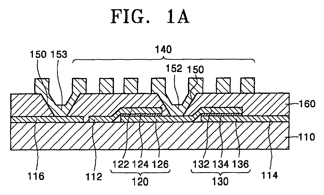
- FIGS. 1A and 1B are a schematic cross-sectional view and a partial perspective view of a high-pass filter (HPF) which is a passive device for a transceiver according to a first embodiment of the present invention.
- FIG. 2 is an equivalent circuit diagram of the HPF shown in FIGS. 1A and 1B. As shown in FIG. 2, the HPF has a basic circuit configuration in which one inductor L is connected in parallel between two capacitors C1 and C2 that are connected in series to each other.
- FIGS. 1A and 1B show that the HPF having this equivalent circuit configuration is stacked on a substrate 110. A first capacitor 120 and a second capacitor 130 are connected in series to each other on the substrate 110.
- a dielectric layer 160 is formed to cover the substrate 110 and the first and second capacitors 120 and 130, and an inductor 140 is formed on the dielectric layer 160.
- the inductor 140 is connected to a connection between the first and second capacitors 120 and 130 underneath the dielectric layer 160 via an electrode 152 that is formed in a via hole 150.
- the substrate 110 is formed of a semiconductor or a dielectric.
- the first and second capacitors 120 and 130 are manufactured by a MEMS technique.
- the first capacitor 120 is composed of a second electrode 126 that is a lower electrode formed on the substrate 110, a first electrode 122 that is an upper electrode opposite to the second electrode 126, and a first dielectric 124 that is interposed between the first and second electrodes 122 and 126.
- the second capacitor 130 is composed of an upper electrode 132 that is formed by extending the second electrode 126, a third electrode 136 that is a lower electrode, and a second dielectric 134 that is interposed between the upper electrode 132 and the third electrode 136.
- An end of the first electrode 122 is connected to an input signal line 112
- an end of the third electrode 136 is connected to an output signal line 114
- a ground 116 is formed beside the input and output signal lines 112 and 114 to transmit radio frequency (RF) signals of the input and output signal lines 112 and 114.
- This ground 116 is connected to an end of the inductor 140 via an electrode 153 that is formed in a via hole 150.
- the signal having a predetermined frequency is transmitted through the first and second capacitors 120 and 130 to the output signal line 114.
- a signal below a predetermined frequency is output through the inductor 140 to the ground 116.
- FIG. 3 is a cross-sectional view of a modified example of the first embodiment. Elements which are the same as those of the first embodiment are denoted with the same reference numerals. Thus detailed descriptions thereof will be omitted.
- a dielectric film 111 is formed on a substrate 110, and an inductor 140 is formed on the dielectric film 111.
- a dielectric layer 160 is formed on the dielectric film 111 to cover the inductor 140.
- the inductor 140 is connected to a connection between the first and second capacitors 120 and 130 on the dielectric layer 160 via an electrode 152 that is formed in a via hole 150.
- the dielectric film 111 is formed of polyimide or benzylchlobutene (BCB) polymer to prevent RF signal loss if the substrate 110 is a semiconductor.
- BCB benzylchlobutene
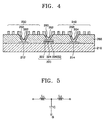
- FIG. 4 is a schematic cross-sectional view of a low-pass filter (LPF) that is a passive device for a transceiver according to a second embodiment of the present invention.
- FIG. 5 is an equivalent circuit diagram of the LPF shown in FIG. 4. As shown in FIG. 5, the LPF has a basic circuit configuration in which one capacitor C is connected in parallel between two inductors L1 and L2.
- FIG. 4 shows that the LPF having this equivalent circuit configuration is stacked on a substrate 210.
- a capacitor 220 is formed on the substrate 210, and a dielectric layer 260 is formed on the substrate 210 to cover the capacitor 220.
- First and second inductors 230 and 240 are connected in series to each other on the dielectric layer 260.
- the capacitor 220 is connected to a connection between the first and second inductors 230 and 240 on the substrate 210 via an electrode 252 that is formed in a via hole 250.
- the substrate 210 is formed of a semiconductor or a dielectric.
- An end of the first inductor 230 is connected to an input signal line 212 on the substrate 210 via an electrode 252
- an end of the second inductor 240 is connected to an output signal line 214 on the substrate 210 via the electrode 254, and a lower electrode 226 of the capacitor 220 is connected to a ground G.
- the capacitor 220 is manufactured by the MEMS technique.
- the capacitor 220 is composed of a lower electrode 226 that is formed on the substrate 210, an upper electrode 222 that is opposite to the lower electrode 226, and a dielectric 224 that is interposed between the lower and upper electrodes 226 and 222.
- the first and second inductors 230 and 240 are manufactured by the MEMS technique and connected to the capacitor 220 via the via hole 250.
- the LPF having the above-described structure, if a signal having a predetermined frequency is input from the input signal line 212 that is connected to an end of the first inductor 230, the signal is transmitted through the first and second inductors 230 and 240 to the output signal line 214 that is connected to the other end of the second inductor 240. A signal above a predetermined frequency is output to the ground G through the capacitor 220.
- FIG. 6 is a cross-sectional view of a modified example of the second embodiment.
- the same reference numerals as those of the first embodiment denote the same elements and their detailed descriptions will be omitted.
- a dielectric film 211 is formed on a substrate 210.
- Two inductors 230 and 240 are formed on the dielectric film 211.
- a dielectric layer 260 is formed on the inductors 230 and 240 to cover the dielectric film 211.
- a connection between the inductors 230 and 240 is connected to a lower electrode 226 of a capacitor 220 on the dielectric layer 260 via an electrode 252 formed in a via hole 250.
- the dielectric film 211 is formed of polyimide or benzylchlobutene (BCB) polymer to prevent RF signal loss if the substrate 210 is a semiconductor.
- BCB benzylchlobutene
- FIG. 7 is an equivalent circuit diagram of a band-bass filter (BPF) that is a passive device for a transceiver according to a third embodiment of the present invention.
- BPF band-bass filter
- a plurality of capacitors C1, C2, C3 and C4 are connected in series to each other.
- Other capacitors C5, C6, and C7 and inductors L1, L2, and L3 are connected in parallel to each other between the capacitors C1, C2, C3, and C4.
- the capacitors C1, C2, C3, C4, C5, C6, and C7 are formed on a substrate and a dielectric layer is formed to cover the capacitors C1, C2, C3, C4, C5, C6, and C7.
- the inductors L1, L2, and L3 are formed on the dielectric layer to be connected to the capacitors C1, C2, C3, C4, C5, C6, and C7 via an electrode (Refer to 152 of FIGS. 1A and 1B and 252 of FIG. 5) formed in a via hole that penetrates through the dielectric layer.
- inductors L1, L2, and L3 are formed on the dielectric film and a dielectric layer is formed to cover the inductors L1, L2, and L3 and the dielectric film.
- Capacitors C1, C2, C3, C4, C5, C6, and C7 are formed on the dielectric layer to be connected to the inductors L1, L2, and L3 via a via hole electrode that penetrates through the dielectric layer.
- the inductors L1, L2, and L3 and the capacitors C1, C2, C3, C4, C5, C6, and C7 are manufactured by the MEMS technique.
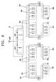
- FIG. 8 is an equivalent circuit diagram of an integrated module that is a passive device for a transceiver according to a fourth embodiment of the present invention.
- This integrated module can be used for two frequency bands: a PCS mode using a transmission and reception frequency in a frequency band of 1.8 GHz and a CDMA mode using a transmission and reception frequency in a frequency band of 0.9 GHz.
- the integrated module that is a passive device for a transceiver is composed of a radio frequency (RF) selector S, duplexers D1 and D2, transmission band-pass filters B3 and B7, and reception band-pass filters B4 and B8.
- the RF selector S identifies a frequency signal from a transmission and reception antenna ANT.
- Duplexers D1 and D2 receive and switch a signal received from the transmission and reception antenna ANT and a signal that will be transmitted to the transmission and reception antenna ANT.
- Transmission band-pass filters B3 and B7 filter a signal that will be transmitted to the duplexers D1 and D2.
- Reception band-pass filters B4 and B8 filter a signal received from the duplexers D1 and D3.
- the RF selector S includes a HPF and a LPF which are the same as those described in the first and second embodiments, respectively.
- the duplexers D1 and D2 include transmission filters B1 and B5, respectively, and reception filters B2 and B6, respectively, which are composed of band-pass filters described in the third embodiment.
- a plurality of capacitors are connectedly formed on the substrate as previously described and a dielectric layer is formed on the substrate to cover the capacitors.
- Inductors are formed on the dielectric layer to be connected to the capacitors via an electrode (Refer to 152 of FIGS. 1A and 1B and 252 of FIG. 5) formed in a via hole that penetrates through the dielectric layer.
- a thin dielectric film is formed on the substrate.
- inductors are formed on the thin dielectric film, and then a dielectric layer is formed to cover the inductors and the substrate.
- Capacitors are formed on the dielectric layer to be connected to the inductors via a via hole electrode that penetrates through the dielectric layer.
- the integrated module having the above-described structure serves as a radio transceiver connected to an external integrated circuit (IC) including a converter between an audio signal and an electric circuit, a modulator for modulating a low frequency signal into a high frequency signal, an amplifier, etc.
- IC integrated circuit
- Transmission nodes Tx transmit a signal
- the transmission band-pass filters B3 and B7 filter the signal
- power amplifiers (PAs) amplify the signal
- the transmission filters B1 and B5 of the duplexers D1 and D2 filter the signal
- the HPF or LPF transmits the signal to the transmission and reception antenna ANT and then to the outside.
- a signal received from the transmission and reception antenna ANT selects its reception path in the RF selector S based on the frequency of the signal.
- the reception filters B2 and B6 of the duplexers D1 and D2 filter the signal and low noise amplifiers (LNAs) amplify the signal.
- the transmission band-pass filters B4 and B8 filter the signal and output the signal to reception nodes Rx.
- FIG. 9 is an exploded perspective view showing a RF IC prepared on a substrate of the HPF of FIG. 1B, which is used to describe the fourth embodiment of the present invention in detail.
- capacitors 120 and 130 are connected in series to each other on a substrate 110.
- a dielectric layer 160 is formed on the substrate 110 and the capacitors 122 and 132 to cover the substrate 110 and the capacitors 120 and 130.
- An inductor 140 is formed on the dielectric layer 160. The inductor 140 is connected to a connection between the capacitors 120 and 130 underneath the dielectric layer 160 via an electrode 152 formed in a via hole 150.
- the substrate 110 is formed of a semiconductor or a dielectric.
- a plurality of RF integrated circuits (ICs) 184 are connected to a signal line 182 that is connected to the connection between the capacitors 120 and 130.
- FIG. 10 shows a plurality of RF ICs prepared on a substrate of the HPF of FIG. 3, which is used to describe the fourth embodiment of the present invention in detail.
- Like reference numerals in the fourth embodiment denote the same members in the first embodiment and their detailed description will be omitted.
- a dielectric film 111 is formed on a substrate 110, and an inductor 140 is formed on the dielectric film 111. And, a dielectric layer 160 is formed over the dielectric film 111 to cover the inductor 140.
- Two capacitors 120 and 130 are formed on the dielectric layer 160 and a plurality of RF ICs 184 are connected to a signal line 182 that is connected to a connection between the capacitors 120 and 130.
- the RF IC 184 may be an oscillator, a mixer, a LNA or a driver amplifier, and is composed of resistor(s), capacitor(s), and inductor(s).
- the RF IC 184 may be a general discrete device or may be a circuit in which at least one capacitor (not shown) is formed on a first surface of the dielectric layer 160, at least one inductor (not shown) is formed on a second surface of the dielectric layer 160, and an electrode formed on a via hole connects the capacitor to the inductor by the method of the previous embodiments.
- a reduction in the area required for mounting passive devices and modules thereof according to the present invention contributes to the downsizing of communication systems. Also, use of the MEMS technique can reduce insertion loss of inductors, which improves the communication quality of communication systems.
Landscapes
- Engineering & Computer Science (AREA)
- Power Engineering (AREA)
- Computer Networks & Wireless Communication (AREA)
- Signal Processing (AREA)
- Semiconductor Integrated Circuits (AREA)
- Filters And Equalizers (AREA)
- Transceivers (AREA)
Abstract
Description
FIG. 8 is an equivalent circuit diagram of an integrated module that is a passive device for a transceiver according to a fourth embodiment of the present invention. This integrated module can be used for two frequency bands: a PCS mode using a transmission and reception frequency in a frequency band of 1.8 GHz and a CDMA mode using a transmission and reception frequency in a frequency band of 0.9 GHz.
Claims (14)
- A passive device for a transceiver comprising:one of a semiconductor substrate and a dielectric substrate;at least one capacitor which is formed on the substrate;a dielectric layer which is formed on the capacitor and the substrate;at least one inductor which is formed on the dielectric layer;a via hole which penetrates through the dielectric layer;a metal electrode which is formed in the via hole and electrically connects the capacitor and the inductor;radio frequency signal lines for the inductor and the capacitor; anda radio frequency ground which is formed on the substrate and isolated from the radio frequency signal lines.
- A passive device for a transceiver comprising:one of a semiconductor substrate and a dielectric substrate;at least one inductor which is formed on the substrate;a dielectric layer which is formed to cover the substrate and the inductor;at least one capacitor which is formed on the dielectric layer;a via hole which penetrates through the dielectric layer;a metal electrode which is formed on the via hole and electrically connects the capacitor and the inductor;radio frequency signal lines for the inductor and the capacitor; anda radio frequency ground which is formed on the dielectric layer and isolated from the radio frequency signal lines.
- The passive device for a transceiver of claim 2, further comprising a dielectric film that is formed between the substrate and the inductor.
- The passive device of claim 1 or 2, wherein a high-pass filter is formed of two capacitors and one inductor and the inductor is connected in parallel to the capacitors via the via hole.
- The passive device of claim 1 or 2, wherein a low-pass filter is formed of one capacitor and two inductors and the capacitor is connected in parallel to the inductors via the via hole.
- The passive device of claim 1 or 2, wherein a band-pass filter is formed of a plurality of capacitors that are connected to each other in series, capacitors that are connected in parallel between the capacitors connected in series, and inductors that are connected in parallel between the capacitors that are connected in series via the via hole.
- An integrated module for a transceiver comprising:wherein a circuit is formed of the capacitors, the inductors, and the radio frequency signal lines, the circuit comprising:one of a semiconductor substrate and a dielectric substrate;a plurality of capacitors which are formed on the substrate;a dielectric layer which is formed on the capacitors and the substrate;a plurality of inductors which are formed on the dielectric layer;via holes which penetrate through the dielectric layer;a plurality of metal electrodes which are formed in the via holes and electrically connect the capacitors and the inductors;radio frequency signal lines for the inductors and the capacitors; anda plurality of radio frequency grounds which are formed on the substrate and isolated from the radio frequency signal lines,a radio frequency selector which is composed of a high-pass filter and a low-pass filter;duplexers which include transmission filters that transmit a signal to the radio frequency selector and are composed of band-pass filters, and reception filters that receive a signal from the radio frequency selector and are composed of band-pass filters;transmission band-pass filters which transmit a signal to the transmission filters via power amplifiers; andreception band-pass filters which receive a signal from the reception filters via low noise amplifiers.
- An integrated module for a transceiver comprising:wherein a circuit is formed of the capacitors, the inductors, and the radio frequency signal lines, the circuit comprising:one of a semiconductor substrate and a dielectric substrate;a plurality inductors which are formed on the substrate;a dielectric layer which is formed to cover the substrate and the inductors;a plurality of capacitors which are formed on the dielectric layer;a plurality via holes which penetrate through the dielectric layer;a plurality of metal electrodes which are formed on the via holes and electrically connect the capacitors and the inductors;radio frequency signal lines for the inductor and the capacitor; anda plurality of radio frequency grounds which are formed on the dielectric layer and isolated from the radio frequency signal lines,a radio frequency selector which is composed of a high-pass filter and a low-pass filter;duplexers which include transmission filters that transmit a signal to the radio frequency selector and are composed of band-pass filters, and reception filters that receive a signal from the radio frequency selector and are composed of band-pass filters;transmission band-pass filters which transmit a signal to the transmission filters via power amplifiers; andreception band-pass filters which receive a signal from the reception filters via low noise amplifiers.
- The integrated module for a transceiver of claim 8, further comprising a dielectric film that is formed between the substrate and the inductor.
- The integrated module of claim 7 or 8, further comprising at least one radio frequency integrated circuit which is connected to the capacitors on the substrate.
- The integrated module of claim 10, wherein the radio frequency integrated circuit is one of a discrete device and a circuit which includes at least one capacitor that is formed on the substrate, at least one inductor that is formed on the dielectric layer, and an electrode that is formed on a via hole and electrically connects the capacitor and the inductor.
- The integrated module of claim 7 or 8, wherein the high-pass filter comprises two capacitors and one inductor and the inductor is connected in parallel to the capacitors via the via hole.
- The integrated module of claim 7 or 8, wherein the low-pass filter comprises one capacitor and two inductors and the capacitor is connected in parallel to the inductors via the via hole.
- The integrated module of claim 7 or 8, wherein the band-pass filter comprises a plurality of capacitors that are connected in series to each other, other, capacitors that are connected in parallel between the capacitors connected in series, and inductors that are connected in parallel between the capacitors that are connected in series via the via hole.
Applications Claiming Priority (2)
| Application Number | Priority Date | Filing Date | Title |
|---|---|---|---|
| KR2001071101 | 2001-11-15 | ||
| KR10-2001-0071101A KR100400234B1 (en) | 2001-11-15 | 2001-11-15 | Passive devices and modules for transceiver |
Publications (3)
| Publication Number | Publication Date |
|---|---|
| EP1313144A2 true EP1313144A2 (en) | 2003-05-21 |
| EP1313144A3 EP1313144A3 (en) | 2003-06-04 |
| EP1313144B1 EP1313144B1 (en) | 2006-03-22 |
Family
ID=36217544
Family Applications (1)
| Application Number | Title | Priority Date | Filing Date |
|---|---|---|---|
| EP02023697A Expired - Lifetime EP1313144B1 (en) | 2001-11-15 | 2002-10-22 | Passive devices and modules for transceiver |
Country Status (6)
| Country | Link |
|---|---|
| US (1) | US7109825B2 (en) |
| EP (1) | EP1313144B1 (en) |
| JP (1) | JP2003283286A (en) |
| KR (1) | KR100400234B1 (en) |
| CN (1) | CN1265561C (en) |
| DE (1) | DE60209980T2 (en) |
Cited By (1)
| Publication number | Priority date | Publication date | Assignee | Title |
|---|---|---|---|---|
| EP1825528A4 (en) * | 2004-12-09 | 2009-11-11 | Wispry Inc | POLE-ZERO ELEMENTS AND ASSOCIATED SYSTEMS AND METHODS |
Families Citing this family (23)
| Publication number | Priority date | Publication date | Assignee | Title |
|---|---|---|---|---|
| DE102004016399B4 (en) * | 2003-03-27 | 2013-06-06 | Kyocera Corp. | High frequency module and radio device |
| TWI231106B (en) * | 2003-12-10 | 2005-04-11 | Kinpo Elect Inc | Wireless transmitting/receiving circulator circuit |
| JP2005175262A (en) * | 2003-12-12 | 2005-06-30 | Renesas Technology Corp | Semiconductor device and manufacturing method thereof |
| JP4418250B2 (en) * | 2004-02-05 | 2010-02-17 | 株式会社ルネサステクノロジ | High frequency circuit module |
| JP4707056B2 (en) * | 2005-08-31 | 2011-06-22 | 富士通株式会社 | Integrated electronic component and integrated electronic component manufacturing method |
| JP4506722B2 (en) * | 2006-05-19 | 2010-07-21 | ソニー株式会社 | Semiconductor element coupling device, semiconductor element, high-frequency module, and semiconductor element coupling method |
| JP4702178B2 (en) * | 2006-05-19 | 2011-06-15 | ソニー株式会社 | Semiconductor coupling device, semiconductor element, and high-frequency module |
| US8467169B2 (en) | 2007-03-22 | 2013-06-18 | Research In Motion Rf, Inc. | Capacitors adapted for acoustic resonance cancellation |
| US7936553B2 (en) | 2007-03-22 | 2011-05-03 | Paratek Microwave, Inc. | Capacitors adapted for acoustic resonance cancellation |
| US8212155B1 (en) * | 2007-06-26 | 2012-07-03 | Wright Peter V | Integrated passive device |
| KR101499948B1 (en) * | 2007-07-23 | 2015-03-09 | 엘지이노텍 주식회사 | Intergrated communication module |
| JP2010040882A (en) * | 2008-08-07 | 2010-02-18 | Murata Mfg Co Ltd | Electronic component |
| KR200454385Y1 (en) * | 2008-12-15 | 2011-06-30 | 맥스파워(주) | Sealing device |
| WO2012087287A1 (en) * | 2010-12-20 | 2012-06-28 | Intel Corporation | Integrated digital- and radio-frequency system-on-chip devices with integral passive devices in package substrates, and methods of making same |
| US8836078B2 (en) * | 2011-08-18 | 2014-09-16 | Taiwan Semiconductor Manufacturing Company, Ltd. | Vertically oriented inductor within interconnect structures and capacitor structure thereof |
| US10135134B2 (en) | 2012-06-21 | 2018-11-20 | Richwave Technology Corp. | Antenna system for receiving and transmitting wireless signals |
| TWI511479B (en) | 2012-06-21 | 2015-12-01 | Richwave Technology Corp | Antenna system for receiving and transmitting wireless signals |
| CN103280615A (en) * | 2013-06-20 | 2013-09-04 | 南通大学 | Reconfigurable microwave low-pass filter with MEMS switch |
| CN103515095A (en) * | 2013-10-11 | 2014-01-15 | 大连天壹电子有限公司 | Method for manufacturing electromagnetic interference filter of dry laminated ceramic capacitor |
| TWI552174B (en) * | 2014-01-02 | 2016-10-01 | 矽品精密工業股份有限公司 | Electrical circuit structure |
| CN104600059B (en) * | 2015-02-03 | 2017-06-30 | 华进半导体封装先导技术研发中心有限公司 | A kind of TSV pore structures and its processing method with IPD |
| CN106252389B (en) * | 2016-09-05 | 2023-03-21 | 飞昂创新科技南通有限公司 | Anti-interference semiconductor device for optical transceiver |
| JP2022147628A (en) * | 2021-03-23 | 2022-10-06 | 株式会社東芝 | Semiconductor device |
Family Cites Families (8)
| Publication number | Priority date | Publication date | Assignee | Title |
|---|---|---|---|---|
| US5370766A (en) * | 1993-08-16 | 1994-12-06 | California Micro Devices | Methods for fabrication of thin film inductors, inductor networks and integration with other passive and active devices |
| US5739560A (en) | 1994-09-22 | 1998-04-14 | Nippon Telegraph And Telephone Corporation | High frequency masterslice monolithic integrated circuit |
| US5874770A (en) | 1996-10-10 | 1999-02-23 | General Electric Company | Flexible interconnect film including resistor and capacitor layers |
| US6075713A (en) * | 1997-04-15 | 2000-06-13 | Motorola, Inc. | Laser trimmable electronic device |
| US5915188A (en) | 1997-12-22 | 1999-06-22 | Motorola, Inc. | Integrated inductor and capacitor on a substrate and method for fabricating same |
| KR100580162B1 (en) * | 1999-10-15 | 2006-05-16 | 삼성전자주식회사 | Thin-film bandpass filter and manufacturing method thereof |
| JP3680683B2 (en) | 2000-03-06 | 2005-08-10 | 株式会社村田製作所 | Insulator porcelain composition |
| US6477031B1 (en) * | 2000-03-22 | 2002-11-05 | Tdk Corporation | Electronic component for high frequency signals and method for fabricating the same |
-
2001
- 2001-11-15 KR KR10-2001-0071101A patent/KR100400234B1/en not_active Expired - Fee Related
-
2002
- 2002-09-30 US US10/259,427 patent/US7109825B2/en not_active Expired - Lifetime
- 2002-10-22 DE DE60209980T patent/DE60209980T2/en not_active Expired - Lifetime
- 2002-10-22 EP EP02023697A patent/EP1313144B1/en not_active Expired - Lifetime
- 2002-10-22 CN CNB021470103A patent/CN1265561C/en not_active Expired - Fee Related
- 2002-11-13 JP JP2002329191A patent/JP2003283286A/en active Pending
Cited By (2)
| Publication number | Priority date | Publication date | Assignee | Title |
|---|---|---|---|---|
| EP1825528A4 (en) * | 2004-12-09 | 2009-11-11 | Wispry Inc | POLE-ZERO ELEMENTS AND ASSOCIATED SYSTEMS AND METHODS |
| EP2445107A3 (en) * | 2004-12-09 | 2012-09-12 | Wispry, Inc. | Pole-zero elements and related systems and methods |
Also Published As
| Publication number | Publication date |
|---|---|
| EP1313144A3 (en) | 2003-06-04 |
| DE60209980T2 (en) | 2006-08-17 |
| CN1265561C (en) | 2006-07-19 |
| US7109825B2 (en) | 2006-09-19 |
| US20030090882A1 (en) | 2003-05-15 |
| CN1420637A (en) | 2003-05-28 |
| JP2003283286A (en) | 2003-10-03 |
| KR100400234B1 (en) | 2003-10-01 |
| EP1313144B1 (en) | 2006-03-22 |
| KR20030040690A (en) | 2003-05-23 |
| DE60209980D1 (en) | 2006-05-11 |
Similar Documents
| Publication | Publication Date | Title |
|---|---|---|
| US7109825B2 (en) | Passive devices and modules for transceiver | |
| US6649998B2 (en) | Passive devices and modules for transceiver | |
| CN100594675C (en) | Duplexer | |
| US8315577B2 (en) | Multiband high-frequency circuit, multiband high-frequency circuit device and multiband communications apparatus comprising same | |
| US7339445B2 (en) | BAW duplexer without phase shifter | |
| CN100372241C (en) | RF transceiver module formed by multilayer ceramics | |
| US8130787B2 (en) | High-frequency circuit device, and communications apparatus comprising same | |
| US7190970B2 (en) | Multiplexer | |
| US8081047B2 (en) | Multi-band circuit with first and second signal branches | |
| US8620244B2 (en) | Electrical component with a front-end circuit | |
| US20050107042A1 (en) | Transmitter and/or receiver module | |
| US7454178B2 (en) | Low-loss transmitter module | |
| US20060087387A1 (en) | Frequency filtering circuit for wireless communication devices | |
| US20060058000A1 (en) | Integrated radio frequency module | |
| US20210329778A1 (en) | Radio frequency module and communication device | |
| US7389090B1 (en) | Diplexer circuit for wireless communication devices | |
| KR100700967B1 (en) | Front end module of the mobile terminal | |
| CN114830541B (en) | High frequency module and communication device | |
| TWI282667B (en) | Passive devices and modules for transceiver | |
| KR20040076680A (en) | Manufacturing method of triple band front end module | |
| KR20060020484A (en) | How to connect saw filter and switch | |
| KR20080078481A (en) | Integrated Communication Module |
Legal Events
| Date | Code | Title | Description |
|---|---|---|---|
| PUAI | Public reference made under article 153(3) epc to a published international application that has entered the european phase |
Free format text: ORIGINAL CODE: 0009012 |
|
| PUAL | Search report despatched |
Free format text: ORIGINAL CODE: 0009013 |
|
| AK | Designated contracting states |
Designated state(s): AT BE BG CH CY CZ DE DK EE ES FI FR GB GR IE IT LI LU MC NL PT SE SK TR |
|
| AX | Request for extension of the european patent |
Extension state: AL LT LV MK RO SI |
|
| AK | Designated contracting states |
Designated state(s): AT BE BG CH CY CZ DE DK EE ES FI FR GB GR IE IT LI LU MC NL PT SE SK TR |
|
| AX | Request for extension of the european patent |
Extension state: AL LT LV MK RO SI |
|
| RIC1 | Information provided on ipc code assigned before grant |
Ipc: 7H 05K 1/16 B Ipc: 7H 01L 23/66 A Ipc: 7H 01L 27/06 B |
|
| 17P | Request for examination filed |
Effective date: 20031118 |
|
| AKX | Designation fees paid |
Designated state(s): DE FI FR GB SE |
|
| 17Q | First examination report despatched |
Effective date: 20040204 |
|
| GRAP | Despatch of communication of intention to grant a patent |
Free format text: ORIGINAL CODE: EPIDOSNIGR1 |
|
| GRAS | Grant fee paid |
Free format text: ORIGINAL CODE: EPIDOSNIGR3 |
|
| GRAA | (expected) grant |
Free format text: ORIGINAL CODE: 0009210 |
|
| AK | Designated contracting states |
Kind code of ref document: B1 Designated state(s): DE FI FR GB SE |
|
| REG | Reference to a national code |
Ref country code: GB Ref legal event code: FG4D |
|
| REF | Corresponds to: |
Ref document number: 60209980 Country of ref document: DE Date of ref document: 20060511 Kind code of ref document: P |
|
| REG | Reference to a national code |
Ref country code: SE Ref legal event code: TRGR |
|
| ET | Fr: translation filed | ||
| PLBE | No opposition filed within time limit |
Free format text: ORIGINAL CODE: 0009261 |
|
| STAA | Information on the status of an ep patent application or granted ep patent |
Free format text: STATUS: NO OPPOSITION FILED WITHIN TIME LIMIT |
|
| 26N | No opposition filed |
Effective date: 20061227 |
|
| REG | Reference to a national code |
Ref country code: FR Ref legal event code: PLFP Year of fee payment: 15 |
|
| REG | Reference to a national code |
Ref country code: FR Ref legal event code: PLFP Year of fee payment: 16 |
|
| REG | Reference to a national code |
Ref country code: FR Ref legal event code: PLFP Year of fee payment: 17 |
|
| PGFP | Annual fee paid to national office [announced via postgrant information from national office to epo] |
Ref country code: FI Payment date: 20190920 Year of fee payment: 18 Ref country code: SE Payment date: 20190923 Year of fee payment: 18 Ref country code: FR Payment date: 20190923 Year of fee payment: 18 |
|
| PGFP | Annual fee paid to national office [announced via postgrant information from national office to epo] |
Ref country code: GB Payment date: 20190923 Year of fee payment: 18 |
|
| PGFP | Annual fee paid to national office [announced via postgrant information from national office to epo] |
Ref country code: DE Payment date: 20190920 Year of fee payment: 18 |
|
| REG | Reference to a national code |
Ref country code: DE Ref legal event code: R119 Ref document number: 60209980 Country of ref document: DE |
|
| REG | Reference to a national code |
Ref country code: FI Ref legal event code: MAE |
|
| REG | Reference to a national code |
Ref country code: SE Ref legal event code: EUG |
|
| GBPC | Gb: european patent ceased through non-payment of renewal fee |
Effective date: 20201022 |
|
| PG25 | Lapsed in a contracting state [announced via postgrant information from national office to epo] |
Ref country code: FR Free format text: LAPSE BECAUSE OF NON-PAYMENT OF DUE FEES Effective date: 20201031 Ref country code: FI Free format text: LAPSE BECAUSE OF NON-PAYMENT OF DUE FEES Effective date: 20201022 Ref country code: DE Free format text: LAPSE BECAUSE OF NON-PAYMENT OF DUE FEES Effective date: 20210501 |
|
| PG25 | Lapsed in a contracting state [announced via postgrant information from national office to epo] |
Ref country code: SE Free format text: LAPSE BECAUSE OF NON-PAYMENT OF DUE FEES Effective date: 20201023 Ref country code: GB Free format text: LAPSE BECAUSE OF NON-PAYMENT OF DUE FEES Effective date: 20201022 |