EP1303045A2 - Programmierbare logische Vorrichtung mit redundanter Schaltung - Google Patents
Programmierbare logische Vorrichtung mit redundanter Schaltung Download PDFInfo
- Publication number
- EP1303045A2 EP1303045A2 EP02257103A EP02257103A EP1303045A2 EP 1303045 A2 EP1303045 A2 EP 1303045A2 EP 02257103 A EP02257103 A EP 02257103A EP 02257103 A EP02257103 A EP 02257103A EP 1303045 A2 EP1303045 A2 EP 1303045A2
- Authority
- EP
- European Patent Office
- Prior art keywords
- row
- connections
- redundant
- lines
- stitching
- Prior art date
- Legal status (The legal status is an assumption and is not a legal conclusion. Google has not performed a legal analysis and makes no representation as to the accuracy of the status listed.)
- Withdrawn
Links
Images


Classifications
-
- H—ELECTRICITY
- H03—ELECTRONIC CIRCUITRY
- H03K—PULSE TECHNIQUE
- H03K19/00—Logic circuits, i.e. having at least two inputs acting on one output; Inverting circuits
- H03K19/02—Logic circuits, i.e. having at least two inputs acting on one output; Inverting circuits using specified components
- H03K19/173—Logic circuits, i.e. having at least two inputs acting on one output; Inverting circuits using specified components using elementary logic circuits as components
- H03K19/177—Logic circuits, i.e. having at least two inputs acting on one output; Inverting circuits using specified components using elementary logic circuits as components arranged in matrix form
- H03K19/17748—Structural details of configuration resources
- H03K19/17764—Structural details of configuration resources for reliability
-
- H—ELECTRICITY
- H03—ELECTRONIC CIRCUITRY
- H03K—PULSE TECHNIQUE
- H03K19/00—Logic circuits, i.e. having at least two inputs acting on one output; Inverting circuits
- H03K19/02—Logic circuits, i.e. having at least two inputs acting on one output; Inverting circuits using specified components
- H03K19/173—Logic circuits, i.e. having at least two inputs acting on one output; Inverting circuits using specified components using elementary logic circuits as components
- H03K19/177—Logic circuits, i.e. having at least two inputs acting on one output; Inverting circuits using specified components using elementary logic circuits as components arranged in matrix form
- H03K19/17736—Structural details of routing resources
- H03K19/17744—Structural details of routing resources for input/output signals
Definitions
- This invention relates to programmable logic devices having redundant circuitry.
- PLDs Programmable logic devices
- PLAs also sometimes referred to as PALs, PLAs, FPLAs, EPLDs, EEPLDs, LCAs, or FPGAs
- PLDs Programmable logic devices
- PLAs PLAs
- FPLAs FPLAs
- EPLDs EEPLDs
- LCAs LCAs
- FPGAs Programmable logic devices
- Such devices are well known in the art and typically provide an "off the shelf' device having at least a portion that can be electrically programmed to meet a user's specific needs.
- ASICs Application specific integrated circuits
- ASICs Application specific integrated circuits
- PLD as used herein will be considered broad enough to not necessarily exclude such devices.
- programmable logic devices are susceptible to manufacturing defects.
- programmable logic devices may be provided with spare or redundant circuits.
- each respective row below a bad row, including the spare row have programmable connections that can be used to replicate the pattern of connections in the row above that respective row. See, for example, U.S. Pat. Nos. 6,201,404 and 6,344,755.
- a programmable logic device is typically made up of logic regions, such as logic array blocks (LABs), which in turn comprise logic elements. Signals are routed to and from the logic regions over vertical and horizontal conductors that form signal paths. Particular circuitry, including, for example, pass gates, multiplexors ("muxes"), and drivers may be used to couple and drive signals onto horizontal or vertical wires, or to receive signals from the horizontal or vertical wires and drive them to the logic regions. Circuitry forming connections between horizontal wires, vertical wires, and logic regions may be programmable.
- a programmable connection is a pass gate coupled to a random access memory bit circuit, the pass gate programmably connecting a vertical wire to an input multiplexor of a logic region.
- the pass gate is open or closed depending on the data in the memory bit.
- Some examples may include connections based upon static or dynamic random access memory, electrically erasable read-only memory, flash, fuse, and anti-fuse programmable connections.
- the programmable connection could also be implemented through mask programming during fabrication of the device. While mask programming may have disadvantages relative to some of the field programmable options already listed, it may be useful in certain high volume applications.
- Horizontal wires may form signal paths that typically exist within, or are associated with, a particular logic region row.
- a spare row if a spare row is utilized, the horizontal wires and associated connections to and from logic regions of a row above the spare row are replaced by those of the spare row.
- Vertical wires typically span several rows, or may even span all the rows on a device.
- Past PLDs with redundancy have had vertical wires that span all or half of the device. Repairable regions that are no larger than the length of a vertical wire rely on connections to and from the same vertical wire in each row within the repairable region.
- a routing architecture that does not rely on horizontal and vertical wires that span a large portion of the device.
- Certain aspects of such an architecture are described in co-pending application entitled "System and Method for Asymmetric Routing Lines" filed January 25, 2002, serial number 10/057,232, and under a common obligation of assignment as the present application.
- a vertical signal path may be broken into multiple wires between two or more rows in several places up and down a device.
- a segmented routing architecture is also staggered (i.e. adjacent vertical signal paths have wires that start and stop at different rather than at the same vertical position), then across a row touched by several different signal paths, it is likely that for any given row, at least one of the vertical signal paths will include multiple wires between that row and an adjacent row.
- Such a routing architecture presented particular challenges to implementing redundancy. For example, to accommodate such an architecture, there is a need to provide repairable regions that have vertical wires starting and stopping within a repairable region. There is a need to provide a PLD with a staggered segmented routing architecture that also has circuitry that accommodates redundancy.
- a staggered segmented IO routing architecture may be useful for routing signals on an input/output ("IO") bus.
- the IOs at the end of a row of logic regions, on the sides of the PLD, may be referred to as horizontal IOs ("HIO"s).
- IO circuitry, including HIO circuitry may be organized in units, sometimes referred to as blocks (these units may be referred to sometimes by other names, e.g., cells, segments, regions, or just "IOs").
- Vertical signal paths of the HIO bus may span several rows of IO blocks.
- Signals routed on an IO bus are often high fanout signals, meaning, for example, that the same signal is delivered to several different IOs. There is a need for a redundancy scheme for an IO bus that can accommodate a staggered segmented routing structure and that can also accommodate the particular needs of IO signals.
- LAB-to-LAB dedicated routing schemes may exist independent of and in addition to the more general routing architecture of the PLD. See, e.g., U.S. Pat. No. 5,260,611. These LAB-to-LAB routing schemes allow groups of LABs to be linked to provide, for example, a larger function block for performing particular types of functions. Carry chains are one type of function that is usefully performed by such dedicated blocks, however, dedicated LAB-to-LAB routing may be useful for other routing purposes. There is a need to implement redundancy for vertical LAB-to-LAB routing architecture spanning multiple rows within a row-based redundancy scheme.
- the present invention provides a programmable logic device including redundant circuitry for connections between logic region rows and signal paths spanning a plurality of logic regions rows, the signal paths each including respective pluralities of lines.
- redundant circuitry is provided for connections between logic region rows and respective lines spanning respective pluralities of logic region rows where the respective lines span fewer rows than are included in a defined repairable region above a spare row.
- normal and redundant stitching circuitry provide routing and redundant routing over signal paths including respective pluralities of lines.
- a stitching multiplexor of a first signal path is used for redundant routing by a second signal path and normal mode connections for one logic region row to drive the second signal path through the stitching multiplexor may overlap with redundant mode connections to drive the first signal path through the stitching multiplexor.
- both upstream and downstream signal paths having pluralities of lines are provided with redundancy on either the same or different track bundles.
- tracks of physical lines and associated stitching and redundant stitching circuitry provide signal paths that may stitch from one track to another in certain rows.
- stubs provide pathways between lines and routing resources of a logic region row and between lines and stitching circuitry.
- the present invention provides redundancy for IO bus signal paths where the signal paths include respective pluralities of lines.
- IO circuitry is provided to listen to a particular IO bus signal path over the same IO buffer in a majority of rows even as the IO bus signal path is provided on different physical lines over the length of the signal path.
- dedicated routing between logic regions in different rows is provided with circuitry to accomplish bypassing rows as needed in normal and redundant modes.
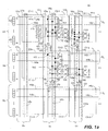
- Figure 1a illustrates a portion of programmable logic device (PLD) having a staggered segmented routing architecture and redundant connections in which an embodiment of the present invention may be implemented.
- PLD programmable logic device
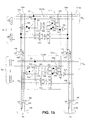
- Figure 1b illustrates further detail with respect to two of the logic region rows illustrated in Figure 1a.
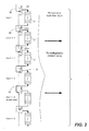
- Figure 2 illustrates a portion of a data register and accompanying switching circuitry that accommodates shifting configuration data to define a repairable region of rows above a spare row.
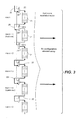
- Figure 3 illustrates the data register and accompanying switching circuitry of Figure 2 configured to shift data to bypass a bad row and to utilize a spare row to repair a repairable region of rows.
- Figure 4 illustrates three logic region rows in a column including a staggered segmented routing architecture and redundant circuitry in accordance with an aspect of the present invention.
- Figure 5 illustrates an embodiment of another aspect of the present invention, the embodiment being an alternative to the embodiment illustrated in Figure 4.
- Figure 6a illustrates an example of logic circuitry for enabling or not enabling the normal or redundant stitching drivers of embodiments of aspects of the present invention.
- Figure 6b is a table illustrating values for the two input signals of the logic circuitry of Figure 6a when no defects exist.
- Figure 6c is a table illustrating values for the two input signals of the logic circuitry of Figure 6a when a defect exists in each repairable region.
- Figure 6d is a table illustrating values of the two input signals of the logic circuitry of Figure 6a when a defect exists in some but not all repairable regions.
- Figure 7 illustrates another embodiment of an aspect of the present invention implemented on signal paths that drive signals upstream against a row shift direction.
- Figure 8 illustrates a portion of several rows within a programmable logic device including a spare row, the portion including multiple physical tracks and being in accordance with aspects of the present invention.
- Figure 9 illustrates signal paths that may be accommodated on the tracks of the portion of Figure 8 when the programmable logic device is configured for normal mode operation.
- Figure 10 illustrates the portion of Figure 8 when the programmable logic device is configured to bypass a bad row and utilize redundant circuitry to provide redundant mode signal paths corresponding to the normal mode signal paths of Figure 9.
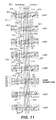
- Figure 11 illustrates a portion of several rows within a programmable logic device including a spare row, the portion having adjacent upstream and downstream physical tracks, normal mode stitching circuitry and redundant mode stitching circuitry being alternated between upstream and downstream physical tracks in accordance with an embodiment of an aspect of the present invention.
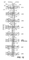
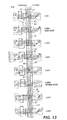
- Figure 12 illustrates signal paths that may be accommodated on the physical tracks of the portion of Figure 11 when the programmable logic device is configured for normal mode operation.
- Figure 13 illustrates the portion of Figure 11 when the programmable logic device is configured to bypass a bad row and utilize redundant circuitry to provide redundant mode signal paths corresponding to the normal mode signal paths of Figure 12 .
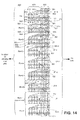
- Figure 14 illustrates an HIO bus portion and additional HIO circuitry having redundant circuitry in accordance with a aspects of the present invention.
- Figure 15 illustrates the HIO bus portion and additional circuitry of Figure 14 configured to provide signal paths in normal mode operation.
- Figure 16 illustrates the HIO bus portion and additional circuitry of Figure 14 configured to provide redundant mode signal paths corresponding to the normal mode signal paths of Figure 15 using redundant circuitry when a bad row exists.
- Figure 17 illustrates a dedicated LAB-to-LAB routing architecture portion configured for normal mode operation in accordance with an aspect of the present invention.
- Figure 18 illustrates the dedicated LAB-to-LAB routing architecture of Figure 17 configured for redundant mode operation to bypass a bad row in a repairable region above a bad row.
- Figure 19 illustrates the dedicated LAB-to-LAB routing architecture of Figure 17 configured to accommodate a bad row in the row just below a spare row.
- Figure 20 illustrates an alternative embodiment of a dedicated LAB-to-LAB routing architecture in accordance an aspect f the present invention.
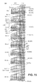
- FIG. 1a illustrates a PLD section 10 of a programmable logic device.
- PLD section 10 includes logic regions comprising logic array blocks (LABs) C1-1, C2-1, C3-1 C1-2, C2-2, C3-2, C1-3, C2-3, and C3-3.
- Each LAB in section 10 has logic elements (LEs) 110. Some LEs 110 are shown individually for LAB C1-1, but are not shown for other LABs.
- Each LAB illustrated is part of a logic region row.
- PLD section 10 includes portions of three logic region rows: R1, R2, and R3.
- Each logic region row of PLD section 10 includes the LABs of the row and further includes a horizontal channel of conductors.
- logic region row R1 includes LABs C1-1, C2-1, and C3-1.
- Logic region row R1 further includes horizontal channel A H that includes two illustrated tracks of horizontal wires.
- a first track includes horizontal wires ("H-lines") H1a and H1b and a second track includes H -lines H2a and H2b.
- a horizontal channel in a logic region row typically includes several more horizontal tracks (which may be grouped in "bundles" of wires), however, the horizontal channels in the logic region rows of PLD section 10 are shown with only two tracks so as not to overcomplicate the drawing with unnecessary detail.
- Each logic region row of PLD section 10 further includes routing resources for coupling to the LEs of each LAB, or for coupling to a horizontal channel.
- routing resources including LAB input muxes ("LIMs”) 131, 132, 133, and 134 for receiving signals that may be selected for routing to the LEs of LAB C2-1 (additional layers of muxing between LIMs and LEs not shown). Additional LIMs 131 and 132 are also shown for routing to the LEs of LAB C3-1.
- Other routing resources illustrated include driver input muxes ("DIMs”) 141 and 142 for receiving signals that may be selected for driving onto, respectively, respectively, H-lines H1b and H2a.
- PLD section 10 also includes vertical channels ("V-channels”) Av, Bv, and Cv.
- Each channel includes a plurality of tracks of wires.
- vertical channel Av includes a first track including vertical wires ("V-lines”) V1a and V1b, a second track including V-lines V2a and V2b, and a third track including V-line V3a.
- a vertical channel in a PLD typically includes many more tracks of V-lines; a "bundle” might include four tracks (or a different number of tracks), however, a "channel” would typically include several bundles.
- Vertical channels B V and C V are each shown with only a single bundle of four tracks so as not to over-complicate the drawing with unnecessary detail.
- V-channels of PLD section 10 couple to the illustrated LABs in a manner that supports 3-sided routing.
- a LAB in PLD section 10 is coupled to an H-channel and also to two V-channels.
- At least some V-lines in PLD section 10 couple to two different LABs in the same logic region row.
- V-line V9a is coupled to LIMs 131 and 132 in LAB C3-1 and V-line V9a is also coupled to LIMs 133 and 134 in LAB C2-1.
- a 3-sided routing architecture is described in more detail in co-pending application entitled "Routing Architecture for a Programmable Logic Device", filed May 5, 2002, serial number , under a common obligation of assignment as the present application and incorporated herein by reference.
- An aspect of the present invention provides redundancy that accommodates a 3-side routing architecture as described below.
- the routing architecture of PLD section 10 is a staggered, segmented routing architecture.
- the segmented aspect of this routing architecture is illustrated by the multiple V-lines and H-lines shown in the tracks of each vertical and horizontal channel.
- the staggered aspect of this routing architecture is illustrated by the fact that wires on two different tracks in the same channel do not necessarily stop and start in the same relative position.
- V-line Via ends between R1 and R2 and V-line V2a ends between rows R2 and R3.
- V-lines and H-lines shown form an interconnect coupling the illustrated array of logic resources (e.g., logic regions and associated routing to and from logic elements).
- logic resources e.g., logic regions and associated routing to and from logic elements.
- Stitching circuitry is shown for V-lines in V-channels Bv and Cv, but is not separately shown for the V-lines in V-channel Av. Stitching circuitry is also not shown for the H-lines in H-channels A H , B H , and C H .
- stitching circuitry includes muxes 160 and drivers 120. Redundant stitching circuitry includes muxes 160 and redundant drivers 121 as will be explained.
- V-line V5a is stitched to V-line V5b by a mux 160 and a driver 120 as shown.
- V-line V5a also includes a tail V5a-t.
- Tail V5a-t is stitched to V-line V5b through a different mux 160 and through a redundant driver 121 as illustrated.
- Tail V4a-t (associated with a V-line ending above row R1 and not separately shown), is stitched to V-line V4b by a mux 160 and a redundant driver 121 as shown.
- V-line V6a is stitched to V-line V6b by a mux 160 and a driver 120 as shown.
- Tail V8a-t (associated with a V-line ending above row R1 and not separately shown), is stitched to V-line V8b by a mux 160 and a redundant driver 121 as shown.
- V-line V9a is stitched to V-line V9b by a mux 160 and a driver 120 as shown.
- V-line V9a also includes a tail V9a-t.
- Tail V9a-t is stitched to V-line V9b through a mux 160 and a redundant driver 121 as illustrated.
- V-line V10a is stitched to V-line V10b through a mux 160 and a driver 120 as illustrated.
- connections 101 and connections 102 couple V-lines to routing resources of a particular logic region row. To illustrate and describe these connections without over complicating the drawings and descriptions, details are shown only for selected connections to selected routing resources in LABs C2-1 and C3-1 of logic region row R1 and LABS C2-2 and C3-2 of logic region row R2. These connections will be described from the perspective of providing routing circuitry in logic region row R2 that can serve as redundant circuitry for logic region row R1 if redundancy were to be engaged and row data would be shifted downward so that row R2 would replace row R3.
- Memory elements 105 hold data for programming each row of PLD section 10. The actual shifting of data associated with particular rows in normal and redundant modes is described in further detail with regard to Figure 2 and Figure 3.
- V-line V5a is coupled by a connector 101 to a driver input mux (“DIM”) 141 (and an associated driver) for routing signals to H-line H1b.
- DIM driver input mux
- V-line V5a is also coupled by connections 101 to LE routing of LAB C2-1 through LAB input mux (“LIM”) 131 and LIM 132 (and associated drivers).
- V-1ine V6a is coupled by connections 101 to, respectively, DIMs 141 and 142 (and associated drivers).
- V-line V6a is also coupled by a connection 101 to LE routing of LAB C2-1 through LIM 131 (and associated driver).
- V-line V7a is coupled by a connection 101 to DIM 142 (and associated driver).
- V-line V7a is also coupled by a connection 101 to LE routing of LAB C2-1 through LIM 131 (and associated driver).
- V-line V9a is coupled by connections 101 both to the LE routing of LAB C2-1 -- through LIMs 133 and 134 (and associated drivers) -- and to the LE routing of LAB C3-1, through LIMs 131 and 132 (and associated drivers).
- V-line V10a is coupled to the LE routing of LAB C3-1 through LIM 131 (and associated driver).
- Connections 101 are “normal mode” connections in the sense that they provide routing options in particular rows assuming a defective row does not exist.
- Connections 102 are “redundant mode” connections in the sense that they provide routing options in, for example, a second row assuming a redundancy mode is engaged and the second logic region row must provide the routing options available in, for example, a first logic region row.
- "Normal mode" connections in a second row may, in some instances, provide the redundant connections for a first row if they provide options to the same routing resources in the second row that were provided by the normal mode connections.
- a connection may, in some instances, be provided both as a normal mode connection and as a redundant mode connection.
- V-line V5b is coupled by a connection 101 to DIM 141 (and associated driver) for routing to H-line H3b.
- Tail V5a-t is coupled by a connection 102 to DIM 141 (and associated driver) for routing to H-line H3b.
- Tail V5a-t is also coupled by a connection 102 for routing to LEs of LAB C2-2 through, respectively, LIM 131 and LIM 132 (and associated drivers).
- row R2 replaces row R2 and thus the connections between tail V5a-t and the routing resources of logic region row R2 replicate the connections between V-line V5a and the routing resources of row R1
- the connections 102 just described coupling tail V5a-t to, respectively, DIM 141, LIM 131, and LIM 132 in LAB C2-2 provide redundancy for the connections 101 previously described coupling V-line V5a to, respectively, DIM 141, LIM 131, and LIM 132 in LAB C2-1.
- V-line V6a is coupled by a connection 102 to DIM 141 for routing to H-line H3b.
- V-line V6a is also coupled by a connection 101 to DIM 142 (and associated driver) for routing to H-line H4a.
- V-line V6a is coupled by a connection 102 to LE routing of LAB C2-2 through LIM 131 (and associated driver), and is coupled by a connection 101 to LE routing of LAB C2-2 through LIM-132 (and associated driver). Note that all connections 101 coupling V-line V6a to routing resources in logic region row R1 are replicated by the connections 101 and 102 coupling V-line V6a to the routing resources of logic region row R2.
- connection 101 in row R2 provides the redundancy for a corresponding connection 101 in row R1, but that in other instances a connection 102 in row R2 provides the redundancy for a connection 101 in row R1.
- the connection 101 in row R2 coupling V-line V6 to DIM 142 in LAB C2-2 exists as a normal mode connection, however, it also may provide a redundant mode connection as it replicates the connection 101 in row R1 that couples V-line V6a to DIM 142 in LAB C2-1.
- a normal mode connection 101 does not exist to replicate the normal mode connection 101 in row R1 coupling V-line V6a to LIM 131, and, therefore, in row R2 a redundant-mode-only connection 102 coupling V-line V6a to LIM 131 in row R2 LAB C2-2 is provided as shown.
- V-line V7a is coupled by connections 101 to DIM 141 and DIM 142 (and associated drivers) for routing to, respectively, H-lines H3b and H4a.
- V-line V7a is also coupled by a connection 101 to LE routing through LIM 131 (and associated driver) as shown.
- the connections present in row R-1 between V-line V7a and routing resources are also provided in corresponding fashion in R2.
- the connection 101 coupling V-line V7a to DIM 142 for routing to H-line H2a in row R1 is replicated in row R2 by the connection 101 coupling V-line V7a to DIM 142 (and associated driver) for routing to H-line H4a.
- connection 101 coupling V-line V-7a to LE routing of LAB C2-1 through LIM 131 in row R1 is matched in row 2 by the connection 101 coupling to LE routing of LAB C2-2 through LIM 131 (and associated driver).
- the connection 102 coupling V-line V-7a to LE routing of LAB C2-1 through LIM 132 in R1 does not necessarily need to be replicated in row R2 since that connection would not be engaged in normal mode operation, but only in a redundant mode (that connection provides redundancy for a connection in an earlier row, earlier row and connection not separately shown.).
- the connections in row R2 need to provide redundancy for the normal mode connections 101 of row R1, but not for the redundant-mode-only connections 102 of row R1.
- tail V9a-t of V-line V9a is coupled by connections 102 to LE routing of LAB C2-2 through, LIM 133 and LIM 134 (and associated drivers) as illustrated.
- Tail V9a-t is also coupled by connections 102 to LE routing of LAB C3-2 through, respectively, LIM 131 and LIM 132.
- LIMs 133 and 134 in LAB C2-2 and LIMs 131 and 132 in LAB C3-2 in row R2 provide redundancy for connections in row R1 coupling V-line V9a through, respectively, LIMs 131 and 132 in LAB C2-1 and LIMs 133 and 134 in LAB C3-1.
- V-line V10a is coupled by connections 101 to LE routing of LAB C3-2 through LIM 131 (and associated driver) and to LE routing of LAB C2-2 through LIM 134 (and associated driver) as shown.
- These "normal mode" connections in row R2 provide redundancy for connections in row R1 coupling V-line V10a through, respectively, LIM 131 of LAB C3-1 and LIM 134 of LAB C2-1.
- connection between V-channel Cv and both LABS C2-1 and C3-1 in row R1 and the provision for connections that provide redundancy for these connections in row R2 coupling V-channel Cv to both LABS C2-2 and C3-2 in row R1 provides one example of redundancy supporting an aspect of a 3-sided routing architecture.
- Figure 1b illustrates additional connections and routing of PLD section 10 of Figure 1a that highlight additional aspects of an example of redundancy supporting additional aspects of a 3-sided routing architecture.
- Figure 1b shows LABS C2-1 and C2-2 in, respectively, logic region rows R1 and R2.
- Figure 1b also shows portions of vertical channels B V and C V and horizontal channels B H and C H previously illustrated and described in Figure 1a and accompanying text.
- horizontal channels B H and C H further include, respectively, V-lines H1-5b and H3-5b.
- Figure 1b shows aspects of a 3-sided routing architecture including LE routing to and from two vertical channels and one horizontal channel in each row and shows an example of how one aspect of the present invention supports redundancy within the context of a 3-sided routing architecture.
- Logic region rows R1 and R2, LABs C2-1 and C2-2 each further include LE outputs 181, 182, 183, and 184.
- LE output 183 of LAB C2-1 is coupled by a connection 101 for routing to H-line H1b through DIM 141 (and associated driver) as shown.
- LE output 184 of LAB C2-1 is coupled by a connection 102 for routing to H-line H2a through DIM 142 (and associated driver) as shown.
- LE outputs 183 and 184 are respectively coupled by respective connections 101 to V-line V9b through DIM 191 (and associated driver) and through a stitching mux 160 and a stitching driver 120 as shown.
- H-lines H1-5b and H2a are respectively coupled by respective connections 101 to the LE routing of LAB C2-1 through, respectively, LIM 131 and 132 (and associated drivers).
- LE outputs 181 and 182 in LAB C2-2 are coupled by, respectively, a connection 101 and a connection 102 to V-line V5b through DIM 191 (and associated driver) and through a stitching mux 160 and a redundant stitching driver 121 as shown.
- LE output 183 of LAB C2-2 is coupled by a connection 101 for routing to H-line H3b through DIM 141 (and associated driver) as shown.
- LE output 184 of LAB C2-2 is coupled by a connection 102 for routing to H-line H4a through a DIM 142 (and associated driver) as shown.
- LE outputs 183 and 184 are coupled by, respectively, a connection 102 and a connection 101 to V-line V9b through DIM 191 (and associated driver) and through a stitching mux 160 and a redundant stitching driver 121 as shown. Also in row R2, H-lines H3-5b and H4a are coupled by, respectively, a connection 101 and a connection 102 to the LE routing of LAB C2-2 through, respectively, LIM 131 and 132 (and associated drivers).
- row R-2 may be used as a replacement for row R1 if redundancy is engaged.
- Figure 2 illustrates a register portion 20 used for shifting configuration data that programs a PLD having redundant circuitry in a spare row.
- Register portion 20 includes shift register segments 21, each shift register segment 21 corresponding to a row to be programmed. Shift register segments 21 are shown corresponding to, respectively, rows n, n+1, n+2, n+3, n+4, and n+5. Data is routed between shift register segments 21 by connections to steering muxes 22 as shown. Steering muxes 22 receive steering data at enable inputs 22-s for determining whether or not a particular shift register segment will receive data from a configuration data stream. As illustrated, a data path is defined between shift register segments 21 over bolded lines 25 based on steering data received at enable input 22-s.
- Enable inputs 22-s instruct each mux 22 to select data at either or neither of two mux inputs for outputting to a particular shift register segment 21.
- configuration data is directed along lines 25 to each of the shift register segments 21 corresponding to each of rows n, n+1, n+2, and n+3 above spare row n+4.
- steering data at inputs 22-s of the mux 22 shown just above the segment 21 corresponding to spare row n+4 directs that mux 22 to bypass that segment 21. Because no row is being replaced, it is not necessary in the particular example shown in Figure 2 to activate programmable connections in the spare row n+4, and therefore, that row's corresponding register segment 21 may be bypassed from the stream of configuration data.
- Figure 3 illustrates the same register portion 20 illustrated in Figure 2 reconfigured to bypass a bad row and utilize a spare row.
- row n+1 is a bad row.
- Steering data at inputs 22-s of the mux 22 shown just above the segment 21 corresponding to the bad row n+1 directs that mux 22 to bypass that segment 21 so that no configuration data is provided to the bad row.
- row replacement begins below the bad row n+1 until the spare row n+5.
- data from the stream of configuration data that would otherwise have been directed to row n+1 is shifted into row n+2.
- the mux 22 just above the segment 21 corresponding to spare row n+4 is directed by data provided at its enable inputs 22 to direct data into that segment 21 corresponding to the spare row.
- spare row n+4's segment 21 has configuration data that otherwise would have been in row n+3's segment 21
- row n+3 has configuration data that otherwise would have been in row n +2's segment 21
- row n+2 has configuration data that otherwise would have been in row n+1's segment 21, had row n+1 not been determined to be a bad row.
- Data determining which row, if any, in a repairable region is bad is held in a separate register such as a fuse register (fuse register not separately shown), and the fuse register provides steering data to inputs 22-s of muxes 22.
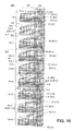
- Figure 4 illustrates a routing architecture 40 with redundant circuitry that illustrates programmable routing in three logic region rows, row x, x+1, and x+2 in a logic region column. Each row illustrated shows the portion of a row associated with one of the logic array blocks (LABs) in that row (LABs not separately shown). Memory elements 405 hold programming data for each illustrated row.
- Memory elements 405 hold programming data for each illustrated row.
- Vertical signal paths 41, 42, 43, and 44 are illustrated including vertical signal paths 41, 42, 43, and 44.
- Vertical signal path 41 includes line 41a;
- vertical signal path 42 includes line 42a, tail 42a-t, and line 42b;
- vertical signal path 43 includes line 43a, tail 43a-t, and line 43b;
- vertical signal path 44 includes line 44a, tail 44a-t, and line 44b.
- Line 42a is stitched to line 42b by stitching circuitry including a stitching mux 410 and a stitching driver 461.
- Tail 42a-t is stitched to line 42b by redundant mux 411 and redundant stitching driver 462.
- Line 43a is stitched to line 43b by stitching circuitry including a stitching mux 410 and a stitching driver 461.
- Tail 43a-t is stitched to line 43b by redundant mux 411 and redundant stitching driver 462.
- Line 44a is stitched to line 44b by stitching circuitry including a stitching mux 410 and a stitching driver 461.
- Routing resources are shown in general form for each row.
- Each row includes logic region routing resources including H-lines 411, 412, 413, 414, LE inputs 421, 422, 423, 424, H-line DIMs 441, 442, 443, and 444, and LE outputs 431, 432, 433, 444.
- Each distinct routing resource is represented by a horizontal line to simplify the drawing and allow better illustration of patterns of connections and redundant connections from row to row.
- the routing resources and associated connections 401 and 402 coupling the routing resources to a particular vertical line include particular combinations of field programmable connections that may be programmed based on data in memory cells 405.
- connections 401 and connections 402 to each routing resource are implemented as pass gates.
- Each LE input (421, 422, 423, and 424) represented is a particular LAB input mux (LIM) .
- LIMs LAB input mux
- Each H-line DIM (441, 442, 443, and 444) represented is a particular driver input mux that connects to the H-line itself.
- An H-line driven by a one of the H-line DIMs may be one of the H lines 411, 412, 413, and 414, or may be different H-lines (different H-lines not separately shown).
- LE outputs 431, 432, 433, and 444 are coupled by connections 100 or 101 to a DIM (DIM not separately shown) for driving a line connected to drive a V-line through a stitching mux 410 or redundant stitching mux 411 as illustrated.
- These types of field programmable connections (i.e. muxes and pass gates) used in the illustrated embodiment are just examples of the types of connections that might be used to couple V-lines to the resources of a particular logic region row.
- connections to the resources of a particular row might represent various combinations of field re-programmable, hard-wired, fuse programmable, or other types of indirect or direct connections that may or may not include a tristate or other driver circuitry.
- Groups 440 of connections 401 and 402 are coupled to drive signals from V-lines to routing resources of a logic region row.
- Groups 450 of connections 401 and 402 are coupled to drive signals from routing resources of a logic region row to particular V-lines. From row to row, patterns of connections 401 and/or 402 in a particular row provide redundancy for similar connections 401 in a preceding row.
- Each row illustrated, i.e., row x, x+1, and x+2 is a row above a spare row within a repairable region. When a redundant mode is engaged, row x+2 replaces row x+1, and row x+1 replaces row x. This will now be described in more detail.
- V-line 41a is coupled by connections 401 to LE inputs 421 and 422. Also in row x, V-line 41a is coupled by connections 401 to H-line DIMs 441 and 442.
- V-line 41a is coupled: to an LE input 421 by a connection 401, to an LE input 422 by a connection 402, and to an LE input 423 by a connection 401.
- the couplings by a connection 401 to an LE input 421 and by a connection 402 to an LE input 422, allow redundancy to be provided in row x+1 for the couplings of signal path 41 to LE inputs 421 and 422 by connection 401 in row x.
- signal path 41 is coupled: to an H-line DIM 441 by a connection 401, to an H-line DIM 442 by a connection 402, and to an H-line DIM 443 by a connection 401.
- the couplings to H-line DIMs 441 and 442 provides redundancy for couplings by connections 401 to H-line DIMS 441 and 442 in row x.
- V-line 41a is coupled: to an LE Input 421 by a connection 401, to an LE input 423 by a connection 402, and to an LE input 424 by a connection 401.
- the coupling of signal path 41 to an LE input 421 by a connection 401 and to an LE input 423 by a connection 402 allow redundancy to be provided in row x+2 for the coupling of signal path 41 to LE inputs 421 and 423 by connections 401 in row x+1.
- signal path 41 is coupled: to an H-line DIM 441 by a connection 401, to an H-line DIM 443 by a connection 402, and to an H-line DIM 444 by a connection 401.
- the coupling of signal path 41 to H-line DIMs 441 and 443 by connections 401 and 402 in row x+2 allows redundancy to be provided for couplings by connections 401 to H-line DIMs 441 and 443 in row x+1.
- line 42a of signal path 42 is coupled: to LE inputs 422 and 423 by connections 401 and to an LE input 424 by a connection 402. Also in row x, line 42a is coupled: to H-line DIMs 442 and 443 by connection 401 and to H-line DIM 444 by a connection 402. As previously described, line 42a is stitched to line 42b through mux 410 and driver 461. Further in row x, H lines 411 and 414 are coupled by connections 401 to provide signals to signal path 42 through stitching mux 410 and stitching driver 461 as shown. LE outputs 432 and 433 are coupled by connections 401 to provide signals to signal path 42 through stitching mux 410 and stitching driver 461 as shown.
- line 42b of signal path 42 is coupled to LE inputs 423 and 424 by connections 401.
- Tail 42a-t of signal line 42a is coupled to LE inputs 422 and 423 by connections 402.
- tail 42a-t is stitched to line 42b through redundant stitching mux 420 and redundant stitching driver 462 as shown.
- the stitching driver 410 between rows x and x+1 is tristated and redundant stitching driver 462 is enabled.
- Connections 402 coupling tail 42a-t to LE inputs 422 and 423 and to H-line DIMs 442 and 443 in row x+1 provide redundancy for the couplings by connections 401 of line 42a to LE inputs 422 and 423 and to H-line DIMs 442 and 443 in row x.
- H lines 411 and 414 are coupled by connections 402 to provide signals to signal path 42 through redundant stitching mux 411 and redundant stitching driver 462. These couplings in row x+1 allow redundancy for the couplings of H lines 411 and 414 by connections 401 signal path 42 in row x.
- LE outputs 432 and 433 are coupled by connections 402 to provide signals to signal path 42 through redundant stitching mux 411 and redundant stitching driver 462 as shown. These couplings in row x+ 1 allow redundancy for the couplings of LE outputs 432 and 433 by connections 401 to signal path 42 in row x.
- line 42b is coupled: to an LE input 422 by a connection 401, to an LE input 423 by a connection 402, and to an LE input 424 by a connection 401.
- the coupling of signal path 42 to an LE input 423 by a connection 402 and to an LE input 424 by a connection 401 allow redundancy to be provided in row x+2 for the coupling of signal path 42 to LE inputs 423 and 424 by connections 401 in row x+1.
- signal path 42 is coupled: to an H-line DIM 442 by a connection 401, to an H-line DIM 443 by a connection 402, and to an H-line DIM 444 by a connection 401.
- the coupling of signal path 42 to H-line DIMs 443 and 444 by connections 402 and 401 in row x+2 allows redundancy to be provided for couplings by connections 401 to H-line DIMs 443 and 444 in row x+1.
- line 43a of signal path 43 is coupled: to an LE input 421 by a connection 401, an LE input 423 by a connection 402, and an LE input and 424 by a connection 401. Also in row x, line 43a is coupled: to an H-line DIM 441 by a connection 401, to an H-line DIM 443 by a connection 402, and to an H-line DIM 444 by a connection 401.
- line 43a of signal path 43 is coupled: to LE inputs 421 and 422 by connections 401 and to an LE input and 424 by a connection 402.
- the coupling of signal path 43 to an LE input 421 by a connection 401 and to an LE input 424 by a connection 402 allow redundancy to be provided in row x+2 for the coupling of signal path 43 to LE inputs 421 and 424 by connections 401 in row x+1.
- line 43a is coupled to H-line DIMs 441 and 442 by connections 401 and to an H-line DIM 444 by a connection 402.
- H lines 413 and 414 are coupled by connections 401 to provide signals to signal path 43 through stitching a mux 410 and a stitching driver 461 as shown.
- LE outputs 432 and 434 are coupled by connections 401 to provide signals to signal path 43 through a stitching mux 410 and a stitching driver 461 as shown.
- line 43b of signal path 43 is coupled to LE inputs 421 and 422 by connections 401.
- Tail 43a-t of line 43a is coupled to LE inputs 421 and 422 by connections 402.
- tail 43a-t is stitched to line 43b through redundant stitching mux 411 and redundant stitching driver 462 as shown.
- the stitching driver 461 between rows x+1 and x+2 is tri-stated and redundant stitching driver 462 on signal path 43 is enabled.
- Connections 402 coupling tail 43a-t to LE inputs 421 and 422 and to H-line DIMs 441 and 442 in row x+2 provide redundancy for the couplings by connections 401 of line 43a to LE inputs 421 and 422 and to H-line DIMs 441 and 442 in row x+1.
- H lines 413 and 414 are coupled by connections 402 to provide signals to signal path 43 through redundant stitching mux 411 and redundant stitching driver 462 as shown.
- line 44a is coupled: to an LE input 421 by a connection 401, to an LE input 422 by a connection 402, and to an LE input 423 by a connection 401.
- V-line 44a is coupled: to an H-line DIM 441 by a connection 401, to an H-line DIM 442 by a connection 402, and to an H-line DIM 443 by a connection 440.
- V-line 44a is coupled: to an LE input 421 by a connection 401, to an LE input 423 by a connection 402, and to an LE input 424 by a connection 401.
- the couplings by a connection 401 to an LE input 421 and by a connection 402 to an LE input 423 allow redundancy to be provided in row x+1 for the couplings of signal path 44 to LE inputs 421 and 423 by connection 401 in row x.
- signal path 44 is coupled: to an H-line DIM 441 by a connection 401, to an H-line DIM 443 by a connection 402, and to an H-line DIM 444 by a connection 401.
- connection 401 and H-line DIM 443 by a connection 402 in row x+1 provide redundancy for couplings of signal path 44 by connections 401 to H-line DIMS 441 and 443 in row x.
- V-line 44a is coupled: to an LE Input 421 by a connection 401, to an LE input 422 by a connection 401, and to an LE input 424 by a connection 402. Note that in row x+2, the coupling of signal path 44 to an LE input 421 by a connection 401 and to an LE input 424 by a connection 402 allow redundancy to be provided in row x+2 for the coupling of signal path 44 to LE inputs 421 and 424 by connections 401 in row x+1.
- signal path 44 is coupled: to an H-line DIM 441 by a connection 401, to an H-line DIM 442 by a connection 401, and to an H-line DIM 444 by a connection 402.
- the coupling of signal path 44 to an H-line DIM 441 by a connection 401 and to an H-line DIM 444 by connections 402 in row x+2 allows redundancy to be provided for couplings of signal path 44 by connections 401 to H-line DIMs 441 and 444 in row x+1.
- H lines 411 and 413 are coupled by connections 401 to provide signals to signal path 44 through stitching mux 410 and driver 461 as shown.
- LE outputs 432 and 433 are coupled by connections 401 to provide signals to signal path 44 through stitching mux 410 and driver 461 as shown. As already described, line 44a is stitched to line 44b as shown. Tail 44a-t provides a redundant path to the next row (next row not shown).
- Signal paths 41-44 of the illustrated architecture 40 are "downstream" meaning that signals are driven in the same direction as the row shift direction for implementing a redundant mode.
- data for each row illustrated is shifted down so that row x is replaced by row x+1, and row x+1 is replaced by row x+2.
- the row shift direction for architecture 40 is down the page from row x to row x+1, to row x+2.
- stitching muxes 410 and drivers 420 as well as redundant stitching muxes are coupled to drive signals down the respective vertical signal paths from row x to row x+1, to row x+2.
- Signal paths 41-44 are provided on a "bundle" of wires within a vertical channel. Architectures for providing redundancy on upstream bundles and on bundles that combine upstream and downstream paths are illustrated and described in subsequent figures and accompanying text (see Figures 7, 11-13 and accompanying text.).
- Figure 5 illustrates a routing architecture 60 with redundant circuitry that illustrates programmable routing in three logic region rows, row y, y+1, and y+2 in a logic region column. Each row illustrated shows the portion of a row associated with one of the logic array blocks (LABs) in that row (LABs not separately shown).
- Vertical signal path 61 includes line 61a;
- vertical signal path 62 includes line 62a, tail 62a-t, and line 62b;
- vertical signal path 63 includes line 63a, tail 63a-t, and line 63b;
- vertical signal path 64 includes line 64a, tail 64a-t, and line 64b.
- Line 62a is stitched to line 62b by stitching circuitry including a stitching mux 610 and a stitching driver 661.
- Tail 62a-t is stitched to line 62b by a stitching mux 610 and redundant stitching driver 662.
- Line 63a is stitched to line 63b by stitching circuitry including a stitching mux 610 and a stitching driver 661.
- Tail 63a-t is stitched to line 63b by a stitching mux 610 and redundant stitching driver 662.
- Line 64a is stitched to line 64b by stitching circuitry including a stitching mux 610 and a stitching driver 661.
- the "normal mode" stitching mux of one signal path is also the "redundant mode” stitching mux of another signal path.
- tail 62a-t (utilized in redundancy) is stitched to line 62b through the same stitching mux 610 that is part of the stitching circuitry stitching line 63a to line 63b.
- routing resources are shown in general form for each row.
- Each row includes logic region routing resources including H-lines 611, 612, 613, 614, LE inputs 621, 622, 623, 624, H-line DIMs 641, 642, 643, and 644, and LE outputs 631, 632, 633, and 634.
- Each distinct routing resource is represented by a horizontal line to simplify the drawing and allow better illustration of patterns of connections and redundant connections from row to row.
- Groups 640 of connections 601 and 602 are coupled to provide signals from V-lines to routing resources of a logic region row.
- Groups 650 of connections 601 and 602 are coupled to provide signals from routing resources of a logic region row to particular V-lines. From row to row, patterns of connections 601 and/or 602 in a particular row, provide redundancy for similar connections 601 in a preceding row.
- Each row illustrated, i.e., row y, y+1, and y+2 is a row above a spare row within a repairable region. When a redundant mode is engaged, row y+2 replaces row y+1, and row y+1 replaces row y. This will now be described in more detail.
- V-line 61a is coupled by connections 601 to LE inputs 621 and 622. Also in row y, V-line 61a is coupled by connections 601 to H-line DIMs 641 and 642.
- V-line 61a is coupled: to an LE input 621 by a connection 601, to an LE input 622 by a connection 602, and to an LE input 623 by a connection 601.
- the couplings by a connection 601 to an LE input 621 and by a connection 602 to an LE input 622 in row y+1 allow redundancy to be provided in row y+1 for the couplings of signal path 61 to LE inputs 621 and 622 by connections 601 in row y.
- signal path 61 is coupled: to an H-line DIM 641 by a connection 601, to an H-line DIM 642 by a connection 602, and to an H-line DIM 643 by a connection 601.
- the couplings of signal path 61 to H-line DIMs 641 and 642 in row y+1 provide redundancy for the couplings by connections 601 to H-line DIMs 641 and 642 in row y.
- V-line 61a is coupled: to an LE Input 621 by a connection 601, to an LE input 623 by a connection 602, and to an LE input 624 by a connection 601.
- the coupling of signal path 61 to an LE input 621 by a connection 601 and to an LE input 623 by a connection 602 in row y+2 allow redundancy to be provided for the coupling of signal path 61 to LE inputs 621 and 623 by connections 601 in row y+1.
- signal path 61 is coupled: to an H-line DIM 641 by a connection 601, to an H-line DIM 643 by a connection 602, and to an H-line DIM 644 by a connection 601.
- line 62a of signal path 62 is coupled: to LE inputs 622 and 623 by connections 601 and to an LE input 624 by a connection 602. Also in row y, line 62a is coupled to H-line DIMs 642 and 643 by connections 601 and to H-line DIM 644 by a connection 602. As previously described, line 62a is stitched to line 62b through stitching mux 610 and stitching driver 661. Further in row y, H lines 611 and 612 are coupled by connections 601 and an H line 613 by a connection 602 to provide signals to signal path 62 through stitching mux 610 and stitching driver 661 as shown. LE outputs 631 and 633 are coupled by connections 601 and an LE output 634 is coupled by a connection 602 to provide signals to signal path 62 through stitching mux 610 and stitching driver 661 as shown.
- line 62b of signal path 62 is coupled to LE inputs 623 and 624 by connections 601.
- Tail 62a-t of line 62a is coupled to LE inputs 622 and 623 and to H-line DIMs 642 and 643 by connections 602
- tail 62a-t is stitched to line 62b through stitching mux 610 and redundant stitching driver 662 as shown.
- the stitching driver 661 between rows y and y+1 is tri-stated and redundant stitching driver 662 between rows y+1 and y+2 is enabled.
- Connections 602 coupling tail 62a-t to LE inputs 622 and 623 and to H-line DIMs 642 and 643 in row y+1 provide redundancy for the couplings of V-line 62a by connections 601 to LE inputs 622 and 623 and to H-line DIMs 642 and 643 in row y. Additional redundancy connections in row y+1 for row y relevant to signal path 62 will be described subsequently in the context of describing signal path 63.
- line 62b is coupled: to an LE input 622 by a connection 601; to an LE input 623 by a connection 602; to an LE input 624 by a connection 601; to an H-line DIM 642 by a connection 601; to an H-line DIM 643 by a connection 602; and to an H-line DIM 644 by a connection 602.
- the couplings of line 62b to: an LE input 623 by a connection 602, an LE input 624 by a connection 602, an H-line DIM 643 by a connection 602 and an H-line DIM 644 by a connection 601 provide redundancy in row y+2 for couplings of line 62b to LE inputs 623 and 624 and H-line DIMs 643 and 644 by connections 601 in row y+1.
- signal path 63 in row y line 63a is coupled: to an LE input 621 by a connection 601; to an LE input 623 by a connection 602; to an LE input 624 by a connection 601; to an H-line DIMs 641 by a connection 601; to an H-line DIM 643 by a connection 602; and to an H-line DIM 644 by a connection 601.
- line 63a is coupled: to LE inputs 621 and 622 by connections 601; to an LE input 624 by a connection 602; to H-line DIMs 641 and 642 by connections 601; and to H-line DIM 644 by a connection 602.
- the coupling of line 63a to an LE input 621 by a connection 601; to an LE input 624 by a connection 602; to an H-line DIM 641 by a connection 601; and to an H-line DIM 644 by a connection 602, all in row y+1, provide redundancy for the couplings of line 63a to LE inputs 621 and 624 and H-line DIMs 641 and 644 in row y.
- Coupling the stitching mux 610 between rows y+1 and y+2 to both a stitching driver 661 for driving signal path 63 and a redundant stitching driver 662 for driving signal path 62 allows some of the illustrated connections 601 coupled for providing signals in normal mode from routing resources to signal path 63 in row y+1 to also provide redundant connections for certain connection coupled to provide signals to signal path 62 in row y. This will now be explained in further detail.
- H lines 611 and 613 are coupled by connections 601 to provide signals in a "normal mode” operation to signal path 63 through stitching mux 610 and stitching driver 661 as shown.
- the coupling of H line 611 by connection 601 also provides "redundant mode” coupling to signal path 62 through stitching mux 610 and redundant driver 662 as shown; this coupling provides redundancy in row y+1 for the coupling of the H-line 611 to signal path 62 by connection 601 in row y.
- H line 612 is coupled by a connection 602 to provide signals in redundant mode operation to signal path 62 through stitching mux 610 and a redundant driver 662 as shown.
- This coupling provides redundancy in row y+1 for the coupling of the H-line 612 to signal path 62 by connection 601 in row y.
- LE outputs 631 and 632 are coupled by connections 601 to provide signals in a "normal mode” operation to signal path 63 through stitching mux 610 and stitching driver 661 as shown.
- the coupling of LE output 631 by connection 601 also provides "redundant mode” coupling to signal path 62 through stitching mux 610 and redundant driver 662 as shown; this coupling provides redundancy in row y+1 for the coupling of the LE output 631 to signal path 62 by connection 601 in row y.
- LE output 633 is coupled by a connection 602 to provide signals in redundant mode operation to signal path 62 through stitching mux 610 and a redundant driver 662 as shown. This coupling provides redundancy in row y+1 for the coupling of the LE output 633 to signal path 62 by connection 601 in row y.
- line 63b is coupled to LE inputs 621 and 622 and to H-line DIMs 641 and 642 by connections 601.
- line 64a of signal path 63 is coupled: to an LE input 621 by a connection 601, an LE input 622 by a connection 602, and an LE input and 623 by a connection 601. Also in row y, line 63a is coupled: to an H-line DIM 641 by a connection 601, to an H-line DIM 642 by a connection 602, and to an H-line DIM 643 by a connection 601.
- V-line 64a is coupled: to an LE input 621 by a connection 601, to an LE input 623 by a connection 602, and to an LE input 624 by a connection 601.
- the couplings by a connection 601 to an LE input 621 and by a connection 602 to an LE input 623 allow redundancy to be provided in row y+1 for the couplings of signal path 64 to LE inputs 621 and 623 by connections 601 in row y.
- signal path 64 is coupled: to an H-line DIM 641 by a connection 601, to an H-line DIM 643 by a connection 602, and to an H-line DIM 644 by a connection 601.
- the couplings of signal path 64 to H-line DIM 641 by a connection 601 and to H-line DIM 643 by a connection 602 in row y+1 provide redundancy for couplings of signal path 64 by connections 601 to H-line DIMs 641 and 643 in row y.
- V-line 64a is coupled: to an LE Input 621 by a connection 601, to an LE input 622 by a connection 601, and to an LE input 624 by a connection 602.
- the coupling of signal path 64 to an LE input 621 by a connection 601 and to an LE input 624 by a connection 602 in row y+2 allow redundancy to be provided for the coupling of signal path 64 to LE inputs 621 and 624 by connections 601 in row y+1.
- signal path 64 is coupled to H-line DIMs 641 and 642 by connections 601 and to an H-line DIM 644 by a connection 602.
- H lines 611 and 614 are coupled by connections 601 to provide signals in a "normal mode” operation to signal path 64 through stitching mux 610 and stitching driver 661 as shown.
- the coupling of H line 611 by connection 601 also provides "redundant mode” coupling to signal path 63 through stitching mux 610 and redundant driver 662 as shown; this coupling provides redundancy in row y+2 for the coupling of the H-line 611 to signal path 63 by connection 601 in row y+1.
- H line 613 is coupled by a connection 602 to provide signals in redundant mode operation to signal path 63 through stitching mux 610 and a redundant driver 662 as shown.
- This coupling provides redundancy in row y+2 for the coupling of the H-line 613 to signal path 63 by connection 601 in row y+1.
- LE outputs 631 and 634 are coupled by connections 601 to provide signals in a "normal mode” operation to signal path 64 through stitching mux 610 and stitching driver 661 as shown.
- the coupling of LE output 631 by connection 601 also provides "redundant mode” coupling to signal path 63 through stitching mux 610 and redundant driver 662 as shown; this coupling provides redundancy in row y+2 for the coupling of the LE output 631 to signal path 62 by connection 601 in row y+1.
- LE output 632 is coupled by a connection 602 to provide signals in redundant mode operation to signal path 63 through stitching mux 610 and a redundant driver 662 as shown. This coupling provides redundancy in row y+2 for the coupling of the LE output 632 to signal path 63 by connection 601 in row y+1.
- FIG. 4 and 5 show V-lines stitching from one to the other.
- a particular V-line may stitch to multiple V-lines.
- the illustrated embodiments also show V-lines stitching from the lowest row before a tail in normal mode or from the tail in redundant mode.
- a particular V-line might stitch to another from other positions on the V-line, such as, for example, the middle of the V-line.
- a connection to another V-line may be viewed as similar to connections to other routing resources, such as the routing resources of a particular logic region.
- the term "stitching" as used herein thus is only meant to provide a convenient label for talking about switching connections between V-lines (i.e.
- connections coupling one V-line to another V-line are not meant to limit the way in which such connections might occur in other embodiments. It is also possible in alternative embodiments for a particular V-line not to stitch to and drive any other V-line. In such various alternatives, a tail might still be used to provide routing and connections over a portion of the V-line in redundant mode that is not used in normal mode.
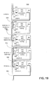
- Figure 6A show an example of logic 70 that may be used to determine whether a stitching driver 720 (comparable to drivers 661 of the embodiment of Figure 5 ) and redundant stitching driver 721 (comparable to drivers 621 of the embodiment of Figure 5 ) should be enabled or turned off.
- stitching driver 720 and redundant stitching driver 721 are coupled to receive signals from the output of stitching mux 710 (comparable to stitching mux 610 of the embodiment of Figure 5 ).
- Logic 70 includes BAD signal generator 71, SHIFT signal generator 72, AND gate 74, and inverters 75.
- a first inverter 75 is coupled to receive a BAD signal and provide inverted output to a first input of AND gate 74 as shown.
- a second inverter 75 and a second input of AND gate 74 are coupled to receive a SHIFT signal as shown.
- the second inverter 75 is coupled to provide an inverted output at an enable input 720EN of stitching driver 720 as shown.
- the AND gate 74 is coupled to provide its output to an enable input 721EN of redundant stitching driver 721 as shown.
- BAD signal generator 71 and SHIFT signal generator 72 are implemented as configuration elements holding either a high or low value. Thus, these configuration elements are receptively coupled to the respective driver 720 and redundant driver 721 through the remaining elements of logic 70.
- logic 70 is just one example of logic that may be utilize to selectively enable or not enable a respective driver and redundant driver.
- configuration elements may be coupled to respective stitching drivers and redundant stitching drivers without the use of intervening logic circuitry. In such embodiments, configuration data will need to account for whether or not a row is a spare row, below a spare row, is a bad row, or is between a bad row and a spare row.
- Figures 6B, 6C, and 6D are tables showing the values of BAD and SHIFT signals provided by signal generators 71 and 72, respectively.
- a stitching driver 720 is turned on and a redundant driver 721 is tristated. This is accomplished as shown by providing low "SHIFT” and "BAD" signals.
- redundancy is not engaged and spare rows are bypassed with both stitching driver 720 and redundant stitching driver 721 being tristated.
- Figure 6C illustrates BAD rows in each repairable region.
- a first repairable region exists above row r3.
- a second repairable region exists above row r6.
- a BAD row exists, thus redundancy is engaged for at least part of both regions.
- rows r2 and r4 are bad.
- Row r1 is a good row. Because row r1 is above BAD row r2 in the repairable region defined above row r3, row shifting for redundancy does not need to be engaged for row r1
- a stitching driver 720 is enabled and a redundant stitching driver 721 is tristated by providing low SHIFT and BAD signals.
- Row r2 is a bad row needing to be bypassed, thus both stitching driver 720 and redundant stitching driver 721 for that row are tristated by providing high SHIFT and BAD signals.
- SPARE row r3 is utilized to replace row r2, and in row r3 redundant stitching driver 721 is enabled and stitching driver 720 is tristated by providing a high SHIFT signal and low BAD signal.
- Row r4 is bad and is bypassed in the same manner indicated for row r2. Row r5 is good.
- Row r5 is below BAD row r4, and with redundancy engaged GOOD row r5 replaces BAD row r4 with stitching driver 720 tristated and redundant driver 721 turned on for row r5, which is accomplished by providing a high SHIFT signal and low BAD signal.
- SPARE row r6 replaces row r5, and a stitching driver 720 is tristated and redundant stitching driver 721 is enabled.
- Figure 6D illustrates a bad row in only some but not all of the repairable regions.
- two repairable regions are defined, a first above row r3 and a second above row r6.
- row r2 is bad.
- Rows r1, r2, and r3 of are treated the same regarding SHIFT and BAD signaling in Figure 6D as in Figure 6C.
- no BAD row exists in the repairable region above row r6 and below row r3, no BAD row exists.
- rows r4, r5, and r6 are treated the same regarding SHIFT and BAD signaling in Figure 6D as in Figure 6B, which defined a part without defects.
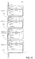
- Figure 7 illustrates upstream wires and associated circuitry providing signal paths in a routing architecture portion 80 with redundant circuitry.
- the wires and associated circuitry provide signal paths in architecture portion 80 that are driven against a row shift direction.
- Figure 7 illustrates programmable routing in three logic region rows: w, w+1, and w+2 in a logic region column. Although signals are driven up the page, the row shift direction when a redundant mode is engaged is down the page. Each row illustrated shows the portion of a row associated with one of the logic array blocks (LABs) in that row (LABs not separately shown).
- LABs logic array blocks
- vertical signal paths 81, 82, 83, and 84 each signal path including a plurality of vertical lines.
- Vertical signal path 81 includes line 81b and tail 81a-t;
- vertical signal path 82 includes line 82a, tail 82a-t, and line 82b;
- vertical signal path 83 includes line 83a, tail 83a-t, and line 83b;
- vertical signal path 84 includes line 84a, and line 84b.
- the lines of each signal path are stitched together by stitching circuitry or redundant stitching circuitry. Stitching connections will be described from bottom to top of the architecture portion 80 as the lines drive signals upstream.
- Line 81b is stitched to tail 81a-t by a mux 810 and a redundant driver 821 (mux and driver between rows w and w+1) as shown.
- Line 82b is stitched to line 82a by stitching circuitry including a stitching mux 810 and a stitching driver 820 as shown.
- Line 82b is also stitched to tail 82a-t by a stitching mux 810 and a redundant stitching driver 821 (mux and redundant driver between rows w+1 and w+2) as shown.
- Line 83b is stitched to line 83a by stitching circuitry including a stitching mux 810 and a stitching driver 820 (mux and driver between rows w+1 and w+2) as shown.
- Line 83b is also stitched to tail 83a-t by stitching circuitry including a stitching mux 810 and a redundant stitching driver 821 (mux and redundant driver at bottom of row w+2) as shown.
- Line 84b is stitched to line 84a by stitching circuitry including a stitching mux 810 and a stitching driver 820 (mux and driver at bottom or row w+2) as shown.
- one aspect of the embodiment of Figure 7 is that the "normal mode" stitching mux of one signal path is also the "redundant mode” stitching mux of another signal path.
- tail 82a-t (utilized in redundancy) is stitched to receive signals from line 82b via a redundant driver 821 through the same stitching mux 810 that is used to couple line 83b to line 83a via normal mode driver 820.
- routing resources are shown in general form for each row.
- Each row includes logic region routing resources including H-lines 811, 812, 813, 814, LE inputs 821, 822, 823, 824, H-line DIMs 841, 842, 843, and 844, and LE outputs 831, 832, 833, and 834 (numbering shown separately only for row w).
- Each distinct routing resource is represented by a horizontal line to simplify the drawing and allow better illustration of patterns of connections and redundant connections from row to row.
- Groups 840 of connections 801 and/or 802 are coupled to provide signals from V-lines to routing resources of a logic region row.
- Groups 850 of connections 801 and 802 are coupled to provide signals from routing resources of a logic region row to particular V-lines. From row to row, patterns of connections 801 and/or 802 in a particular row, provide redundancy for similar connections 801 in a preceding row.
- Each row illustrated, i.e., row w, w+1, and w+2 is a row above a spare row within a repairable region. When a redundant mode is engaged, row w+2 replaces row w+1, and row w+1 replaces row w. This will now be described in more detail.
- V-line 81b is coupled by connections 801 to LE inputs 821 and 822. Also in row w, V-line 81b is coupled by connections 801 to H-line DIMs 841 and 842.
- V-line 81b is coupled: to an LE input 821 by a connection 801, to an LE input 822 by a connection 802, and to an LE input 823 by a connection 801.
- the couplings by a connection 801 to an LE input 821 and by a connection 802 to an LE input 822 in row w+1 allow redundancy to be provided in row w+1 for the couplings of signal path 81 to LE inputs 821 and 822 by connections 801 in row w.
- signal path 81 is coupled: to an H-line DIM 841 by a connection 801, to an H-line DIM 842 by a connection 802, and to an H-line DIM 843 by a connection 801.
- the couplings of signal path 81 to H-line DIMs 841 (a connection 801) and 842 (a connection 802) in row w+1 provide redundancy for the couplings by connections 801 to H-line DIMs 841 and 842 in row w.
- V-line 81b is coupled: to an LE Input 821 by a connection 801, to an LE input 823 by a connection 802, and to an LE input 824 by a connection 801.
- the coupling of signal path 81 to an LE input 821 by a connection 801 and to an LE input 823 by a connection 802 in row w+2 allow redundancy to be provided for the coupling of signal path 81 to LE inputs 821 and 823 by connections 801 in row w+1.
- signal path 81 is coupled: to an H-line DIM 841 by a connection 801, to an H-line DIM 843 by a connection 802, and to an H-line DIM 844 by a connection 801.
- line 82a of signal path 82 is coupled: to LE inputs 822 and 823 by connections 801 and to an LE input 824 by a connection 802. Also in row w, line 82a is coupled to H-line DIMs 842 and 843 by connections 801 and to H-line DIM 844 by a connection 802. As previously described, line 82b is stitched to line 82a through stitching a mux 810 and a stitching driver 820 as shown.
- H lines 811 and 812 are coupled by connections 801 and an H line 813 is coupled by a connection 802 to provide signals to signal path 82 (driving onto line 82a) through stitching mux 810 and stitching driver 820 as shown.
- LE outputs 831 and 833 are coupled by connections 801 and an LE output 834 is coupled by a connection 802 to provide signals to signal path 82 (driving onto line 82a) through stitching mux 810 and stitching driver 820 as shown.
- line 82b of signal path 82 is coupled to LE inputs 823 and 824 by connections 801.
- Tail 82a-t of line 82a is coupled to LE inputs 822 and 823 and to H-line DIMs 832 and 833 by connections 802.
- line 82b stitches to tail 82a-t through stitching mux 810 and redundant stitching driver 821 as shown.
- the stitching driver 820 between rows w and w+1 is tri-stated and redundant stitching driver 821 between rows w+1 and w+2 is enabled.
- Line 82a thus becomes driven in redundancy from the bottom of row w+1 through tail 82a-t rather than from the bottom of row w as in normal mode operation.
- Connections 802 coupling tail 82a-t to LE inputs 822 and 823 and to H-line DIMs 842 and 843 in row w+1 provide redundancy for the couplings of V-line 82a by connections 801 to LE inputs 822 and 823 and to H-line DIMs 842 and 843 in row w. Additional redundancy connections in row w+1 for row w relevant to signal path 82 will be described subsequently in the context of describing signal path 83.
- line 82b is coupled: to an LE input 822 by a connection 801; to an LE input 823 by a connection 802; to an LE input 824 by a connection 801; to an H-line DIM 842 by a connection 801; to an H-line DIM 843 by a connection 802; and to an H-line DIM 844 by a connection 801.
- the couplings of line 82b to: an LE input 823 by a connection 802, an LE input 824 by a connection 801, an H-line DIM 843 by a connection 802 and an H-line DIM 844 by a connection 801 provide redundancy in row w+2 for couplings of line 82b by connections 801 to LE inputs 823 and 824 and H-line DIMs 843 and 844 in row w+1.
- signal path 83 in row w line 83a is coupled: to an LE input 821 by a connection 801; to an LE input 823 by a connection 802; to an LE input 824 by a connection 801; to an H-line DIM 841 by a connection 801; to an H-line DIM 843 by a connection 802; and to an H-line DIM 844 by a connection 801.
- line 83a is coupled: to LE inputs 821 and 822 by connections 801; to an LE input 824 by a connection 802; to H-line DIMS 841 and 842 by connections 801; and to H-line DIM 844 by a connection 802.
- Coupling the stitching mux 810 between rows w+1 and w+2 to both a stitching driver 820 for driving signal path 83 and a redundant stitching driver 821 for driving signal path 82 allows some of the illustrated connections 801 coupled for providing signals in normal mode from routing resources to signal path 83 in row w+1 to also provide redundant connections for certain connections coupled to provide signals to signal path 82 in row w. This will now be explained in further detail.
- H lines 811 and 813 are coupled by connections 801 to provide signals in a normal mode operation to signal path 83 (driving onto line 83a) through stitching mux 810 and stitching driver 820 as shown.
- the coupling of H line 811 by connection 801 also provides redundant mode coupling to signal path 82 through stitching mux 810 and redundant driver 821 driving onto line 82a through tail 82a-t as shown; this coupling provides redundancy in row w+1 for the coupling of the H-line 811 to signal path 82 by connection 801 in row w.
- H line 812 is coupled by a connection 802 to provide signals in redundant mode operation to signal path 82 through stitching mux 810 and a redundant driver 821 driving onto line 82a through tail 82a-t as shown.
- This coupling provides redundancy in row w+1 for the coupling of the H-line 812 to signal path 82 by connection 801 in row w.
- LE outputs 831 and 832 are coupled by connections 801 to provide signals in a normal mode operation to signal path 83 through stitching mux 810 and stitching driver 820 driving onto line 83a as shown.
- connection 801 also provides redundant mode coupling to signal path 82 through stitching mux 810 and redundant driver 821 driving onto line 82a through tail 82a-t as shown; this coupling provides redundancy in row w+1 for the coupling of the LE output 831 to signal path 82 by connection 801 in row w.
- LE output 833 is coupled by a connection 802 to provide signals in redundant mode operation to signal path 82 through a stitching mux 810 and a redundant driver 821 as shown. This coupling provides redundancy in row w+1 for the coupling of the LE output 833 to signal path 82 by connection 801 in row w.
- line 83b is coupled to LE inputs 821 and 822 and to H-line DIMs 841 and 842 by connections 801. These couplings provide redundancy for like coupling by connections 801 in row w+1.
- line 84a of signal path 84 is coupled: to an LE input 821 by a connection 801, an LE input 822 by a connection 802, and an LE input 823 by a connection 801.
- line 83a is coupled: to an H-line DIM 841 by a connection 801, to an H-line DIM 842 by a connection 802, and to an H-line DIM 843 by a connection 801.
- V-line 84a is coupled: to an LE input 821 by a connection 801, to an LE input 823 by a connection 802, and to an LE input 824 by a connection 801. Note that the couplings by a connection 801 to an LE input 821 and by a connection 802 to an LE input 823, allow redundancy to be provided in row w+1 for the couplings of signal path 84 to LE inputs 821 and 823 by connections 801 in row w.
- signal path 84 is coupled: to an H-line DIM 841 by a connection 801, to an H-line DIM 843 by a connection 802, and to an H-line DIM 844 by a connection 801.
- the couplings of signal path 84 to H-line DIM 841 by a connection 801 and to H-line DIM 843 by a connection 802 in row w+1 provide redundancy for couplings of signal path 84 by connections 801 to H-line DIMs 841 and 843 in row w.
- V-line 84a is coupled: to an LE Input 821 by a connection 801, to an LE input 822 by a connection 801, and to an LE input 824 by a connection 802.
- the coupling of signal path 84 to an LE input 821 by a connection 801 and to an LE input 824 by a connection 802 in row w+2 allow redundancy to be provided for the coupling of signal path 84 to LE inputs 821 and 824 by connections 801 in row w+1.
- signal path 84 is coupled to H-line DIMs 841 and 842 by connections 801 and to an H-line DIM 844 by a connection 802.
- connection 801 The coupling of signal path 84 to an H-line DIM 841 by a connection 801 and to an H-line DIM 844 by a connection 802 in row w+2 allows redundancy to be provided for couplings of signal path 84 by connections 801 to H-line DIMs 841 and 844 in row w+1.
- H lines 811 and 814 are coupled by connections 801 to provide signals in a normal mode operation to signal path 84 through stitching mux 810 and stitching driver 820 driving onto line 84a as shown.
- the coupling of H line 811 by connection 801 also provides redundant mode coupling to signal path 83 through stitching mux 810 and redundant driver 821 driving onto line 83a through tail 83a-t as shown; this coupling provides redundancy in row w+2 for the coupling of the H-line 811 to signal path 83 by connection 801 in row w+1.
- H line 813 is coupled by a connection 802 to provide signals in redundant mode operation to signal path 83 through stitching mux 810 and a redundant driver 821 driving line 83a through tail 83a-t as shown.
- This coupling provides redundancy in row w+2 for the coupling of the H-line 813 to signal path 83 by connection 801 in row w+1.
- LE outputs 831 and 834 are coupled by connections 801 to provide signals in a normal mode operation to signal path 84 through stitching mux 810 and stitching driver 820 driving line 84a as shown.
- connection 801 also provides redundant mode coupling to signal path 83 through stitching mux 810 and redundant driver 821 driving line 83a through tail 83a-t as shown; this coupling provides redundancy in row w+2 for the coupling of the LE output 831 to signal path 83 by connection 801 in row w+1.
- LE output 832 is coupled by a connection 802 to provide signals in redundant mode operation to signal path 83 through stitching mux 810 and a redundant driver 821 as shown. This coupling provides redundancy in row w+2 for the coupling of the LE output 832 to signal path 83 by connection 801 in row w+1.
- Figures 8-10 illustrates a portion 700 including multiple rows in a PLD.
- the portion 700 includes 12 rows of LABs, rows LAB1-LAB12.
- portion 700 provides stitching drivers 751 and redundant stitching drivers 752 in a vertical column 780 of drivers 751 and 752.
- portion 700 further includes vertical tracks 1, 2, 3, 4, and 5.
- Each track includes a plurality of individual wires or V-lines.
- track 1 includes V-line tail 1a-t, V-line 1b and tail 1b-t, and V-line 1c and tail 1c-t.
- Track 2 includes V-line 2a and tail 2a-t, V-line 2b and tail 2b-t, and V-line 2c.
- Track 3 includes V-line 3a and tail 3a-t, V-line 3b and tail 3b-t, and V-line 3c.
- Track 4 includes V-line 4a and tail 4a-t, V-line 4b and tail 4b-t, and V-line 4c.
- Track 5 includes V-line 5a and tail 5a-t, V-line 5b and tail 5b-t, and V-line 5c.
- each tail is part of the same wire as its associated V-line and is simply that portion of the wire not used during normal mode operation (e.g. tail 3a-t is part of the same wire that provides V-line 3a).
- tail 3a-t is part of the same wire that provides V-line 3a.
- such a tail may be provided on a different wire than the wire providing the associated V-line (e.g., a wire coupled to the V-line wire) without necessarily departing from the spirit and scope of other aspects of the present invention.
- Portion 700 further includes horizontal stubs H-1, H-2, H-3, H-4, H-5, and H-6.
- Connections 731 and 732 couple V-lines to horizontal stubs as indicated and also couple driver outputs to horizontal stubs as indicated.
- Portion 700 further includes groups 710, 720, and 740 of connections 701 and 702.
- Groups 710 include connections 701 and 702 to DIMs for driving H-lines (H-line DIMs, associated drivers, and H-lines not separately shown)
- groups 720 include connections 701 and 702 for stitching between V-lines through DIMs and drivers 751 or 752 (V-line DIMs not separately shown)
- groups 740 include connections 701 and 702 to LIMs for routing to LEs (LIMs and LEs not separately shown).
- one way to implement a mux is as a collection of pass gates coupled to a common output and programmable to be on or off based on data in configuration elements -- in the case of a one-output mux, only one pass gate is programmed to be "on" at any given time.
- other pass gates connected to the drivers 751 and 752 are not separately shown
- connections 701 and redundant mode connections 702 generally provide redundancy for connections 701 from row to row.
- connections 701 provide LIM connections coupled to V-lines 1b 3a, 4a, and 5a by, respectively, stubs H-5, H-3, H-2, and H-1 of row LAB2 via connections 731 as shown.
- connections 701 and a connection 702 provide LIM connections (group 740) that can become redundant for the connections 701 to LIMs in row LAB2.
- connections 701 and a connection 702 provide redundant LIM connections coupled to V-line 1b (a connection 701), tail 3a-t (a connection 702), V-line 4a (a connection 701), and V-line 5a (a connection 701), by, respectively, stubs H-5, H-3, H-2, and H-1 of row LAB3 via connections 731 and a connection 732 as shown.
- These row LAB3 LIM connections can be used in a redundant mode to replace the row LAB2 LIM connections just described.
- a connection 701 provides a DIM connection coupled to V-line 4a by a stub H-2 of row LAB2 via a connection 731 as shown.
- a connection 702 provides a DIM connection (group 710) that can become redundant for the connection 701 to a DIM in row LAB2.
- a connection 702 provides a redundant DIM connection coupled to V-line 4a by a stub H-2 of row LAB3 via a connection 731 as shown.
- This row LAB3 DIM connection can be used in a redundant mode to replace the row LAB2 DIM connection just described.
- V-lines together with respective tails in each track have an actual length measured in LAB rows spanned (whether or not used) and a logical length measured in LAB rows actually used in a particular mode.
- Actual length refers to the number of rows that the V-line reaches into, not including the row in which the line first exists.
- V-line 1c and tail 1c-t together have an actual length of five (counting rows LABS, LAB9, LAB10, LAB11, and LAB12); by contrast, V-line 2b and tail 2b-t together have an actual length of 6 LAB rows (counting rows LAB3, LAB4, LABS, LAB6, LAB7, and LAB8).
- the logical length is the length that the line is considered to be for purposes of configuration and routing on the device for operation in a particular mode.
- the logical length is measured by counting, beginning with the first row after the row from which the line is first driven, the active rows which the line spans (i.e. in normal mode, not counting spare rows and rows only touching a the line's tail; and in redundant mode, counting spare rows and rows touching the needed portions of the line's tail but not bad rows).
- V-line 1c together with tail 1c-t has an actual length of five and, in normal mode operation, a logical length of four.
- V-line tail Vc-t In normal mode operation, the V-line tail Vc-t is not utilized, and thus rows into which the tail extends are not counted in logical length, thus the logical length of four includes rows LAB8, LAB9, LAB 10, and LAB11.
- V-line 2b together with tail 2b-t has an actual length of 6 and, in normal mode operation, an logical length of four.
- the tail V2b-t In normal mode operation, the tail V2b-t is not utilized and thus not counted for logical length; moreover, the spare row is not utilized, and thus is also not counted in logical length; thus, the logical length of four in normal mode operation includes rows LAB3, LAB4, LABS, and LAB7.
- the actual length of the V-line together with the tail may be either five or six (i.e. one greater or two greater than the desired logical length) and still be consistent with this aspect of the embodiment of Figure 8 .
- V-line 1b does not extend into spare row LAB6, however, tail 1b-t of V-line 1b does extend into spare row LAB6.
- the actual length of V-line 1b together with tail 1b-t is 6.
- the portion of tail 1b-t extending into row LAB7 is not necessary as it is not utilized even in redundant mode operation.
- V-lines may be provided that are all the same actual length. Such embodiments, may, depending on the context, need to account for limited stitching ability in rows prior to a spare row. Such embodiments may also require accounting for similar V-lines having different logical lengths if some V-lines cross spare rows and others do not. For designing routing algorithms, it may be useful in some contexts to provide a layout such as that provided in the aspect of the illustrated embodiment under which the logical length is consistent across wires whether or not a spare row is crossed.
- Figure 9 shows the portion 700 of Figure 8 configured to provide normal mode operation with a spare row at row LAB 6 and routing for four signal paths, 76, 77, 78, and 79. As shown, five physical tracks are used to provide routing for the four signal paths. This allows a portion of each track to be reserved for use in redundant mode operation. As shown, signal paths stitch from 1 track to another through a connection 701 in a connection group 720 in each row. Thus one V-line in a particular signal path is not necessarily in the same physical track as another V-line in the same signal path. These stitching connections will now be described in more detail.
- the signal path 76 is provided on track 2. However, in row LAB 1, the signal path 76 stitches from one V-line to another as follows. It is coupled to a stub H-4 by a connection 731. From stub H-4, it is coupled by a connection 701 to a driver 751 input as shown. From the output of the driver 751 it is coupled to a stub H-6 by a connection 731, and from stub H-6 it is coupled by another connection 731 to a V-line in track 1 as indicated. Signal path 76 continues in track 1 until row LABS where it is coupled by a connection 731 to a stub H-5, which in turn is coupled by a connection 701 to a driver 751 input.
- the output of the driver 751 is coupled by a connection 731 to a stub H-6 which in turn is coupled by another connection 731 to a V-line in track 5 as indicated.
- Signal path 76 continues in track 5 until row LAB 10 where it is coupled by a connection 731 to a stub H-1, which in turn is coupled by a connection 701 to a driver 751 input.
- the output of the driver 751 in row LAB10 is coupled by a connection 731 to a stub H-6 which in turn is coupled by another connection 731 to a V-line in track 4.
- the signal path 77 in row LAB1, the signal path is provided on track 3.
- the signal path 77 stitches from one V-line to another as follows: It is coupled to a stub H-3 by a connection 731. From the stub H-3, it is coupled by a connection 701 to a driver 751 input as shown. From the driver 751 output in row LAB2, it is coupled to a stub H-6 by a connection 731, and from stub H-6 it is coupled by another connection 731 to a V-line in track 2 as indicated.
- Signal path 77 continues in track 2 until row LAB7 where it is coupled by a connection 731 to a stub H-4, which in turn is coupled by a connection 701 to a driver 751 input.
- the output of the driver 751 in row LAB7 is coupled by a connection 731 to a stub H-6 which in turn is coupled by another connection 731 to a V-line in track 1 as indicated.
- Signal path 77 continues in track 1 until row LAB11 where it is coupled by a connection 731 to a stub H-5, which in turn is coupled by a connection 701 to a driver 751 input.
- the output of the driver 751 in row LAB11 is coupled by a connection 731 to a stub H-6 which in turn is coupled by a connection 731 to a V-line in track 5 as indicated.
- signal path 78 in row LAB1, the signal path is provided on track 4.
- the signal path 78 stitches from one V-line to another as follows: It is coupled to a stub H-2 by a connection 731. From the stub H-2, it is coupled by a connection 701 to a driver 751 input as shown. From the driver 751 output in row LAB3, it is coupled to a stub H-6 by a connection 731, and from stub H-6 it is coupled by another connection 731 to a V-line in track 3 as indicated.
- Signal path 78 continues in track 3 until row LAB8 where it is coupled by a connection 731 to a stub H-3, which in turn is coupled by a connection 701 to a driver 751 input.
- the output of the driver 751 in row LAB8 is coupled by a connection 731 to a stub H-6 which in turn is coupled by another connection 731 to a V-line in track 2 as indicated.
- Signal path 78 continues in track 2 until row LAB12 where it is coupled by a connection 731 to a stub H-4, which in turn is coupled by a connection 701 to a driver 751 input.
- the output of the driver 751 in row LAB12 is coupled by a connection 731 to a stub H-6 which in turn is coupled by another connection 731 to a V-line in track 1 as indicated.
- the signal path 79 stitches from one V-line to another as follows: It is coupled to a stub H-1 by a connection 731. From the stub H-1, it is coupled by a connection 701 to a driver 751 input as shown. From the driver 751 output in row LAB4, it is coupled to a stub H-6 by a connection 731, and from stub H-6 it is coupled by another connection 731 to a V-line in track 4 as indicated.
- Signal path 79 continues in track 4 until row LAB9 where it is coupled by a connection 731 to a stub H-2, which in turn is coupled by a connection 701 to a driver 751 input.
- the output of the driver 751 in row LAB9 is coupled by a connection 731 to a stub H-6 which in turn is coupled by another connection to a V-line in track 3 as indicated.
- drivers 751 and 752 are tristated in that row and all four signal paths extend through the row without making stitching connections.
- connection 701 in a group 740 is provided to each signal path via a horizontal stub and a connection 731.
- at least one connection 702 in a LIM connection group 740 is provided between a tail of a vertical track via a horizontal stub and a connection 732.
- each row has one stitching connection. This quantity of connections is facilitated by the use of 6 horizontal stubs per row, or 2 more stubs than the number of signal paths.
- signal paths 76, 77, 78, and 79 each couple to a connection 701 in LIM connection group 740 via, respectively, stubs H-4, H-3, H-2, and H-1 via normal mode connections 731.
- Tail 1a-t couples to a redundant mode connection 702 in LIM connection group 740 via stub H-5 and a redundant mode connection 732.
- stub H-6 is utilized in row LAB 1 so that signal path 76 can stitch from track 2 to track 1 as shown and line 1b is driven in normal mode from a driver 751 in row LAB1 via stub H-6 as shown.
- the same number of connections per row or a different number of connections per row might be obtained through use of the same or a different number of horizontal stubs.
- the illustrated embodiment might be modified to provide 8 stubs and the additional stubs might be utilized to provide additional couplings to additional LIM connections.
- additional couplings from V-lines to LIM connections might be provided using the same number of stubs as illustrated by modifying the illustrated embodiment to provide additional connections per V-line to stubs in the same row, e.g., additional connections coupling the same V-line to two different stubs for connection to different LIMs in the same row.
- Figure 10 shows the portion 700 of Figure 8 configured to implement redundant mode operation in particular region to repair bad rows LAB2 and LAB7.
- Redundant mode operation is engaged to affect routing from bad row LAB2 to spare row LAB6. Redundant mode operation is also engaged to affect routing from bad row LAB 7 through row LAB12. A spare row exists below row LAB12, but is not separately shown.
- Figures 8-10 represent portions of two repairable regions that can each accommodate repair of a bad row. In alternative embodiments, a greater or smaller number of repairable regions may be defined over a similar section by providing spare rows according to the desired number of repairable regions.
- connection LAB1 note that all connections illustrated in Figure 10 are identical to those shown in Figure 9. Since row LAB1 is above bad row LAB2, no shifting of connections from row LAB1 relative to normal mode is necessary. However, beginning from row LAB2, connections are shifted downward to bypass the bad row LAB2 and utilize spare row LAB6 to accommodate the same signal paths and corresponding stitching connections in connection groups 720, DIM connections in connection groups 710, and LIM connections in connection groups 740.
- Stitching connections are shifted downward as follows: in bad row LAB2, drivers 751 and 752 are tristated. Instead of being stitched from track 3 to track 2 in row LAB2 as illustrated in Figure 9 , signal path 77 is stitched from track 3 to track 2 in row LAB3 as illustrated in Figure 10 .
- the signal path 77 connects via tail 3a-t to a redundant mode connection 732 in row LAB3 coupling tail 3a-t to a stub H-3 which in turn is coupled by a redundant mode connection 702 to a redundant driver 752 which drives a V-line in track 2 via a redundant mode connection 732 to a stub H-4 and a connection 731 coupling the stub H-4 to V-line 2b in track 2 as shown.
- signal path 78 connects via tail 4a-t for stitching from track 4 to track 3 in row LAB4 as illustrated.
- signal path 79 connects via tail 5a-t for stitching from track 5 to track 4 in row LABS as illustrated.
- signal path 76 connects via tail 1b-t for stitching from track 1 to track 5 in spare row LAB6 as illustrated.
- signal path 79 connects via tail 4b-t for stitching from track 4 to track 3 in row LAB 10 as illustrated. Instead of being stitched from track 5 to track 4 in row LAB10, signal path 79 connects via tail 5b-t for stitching from track 5 to track 4 in row LAB11 as illustrated. Instead of being stitched from track 1 to track 5 in row LAB11, signal path 76 connects via tail 1c-t for stitching from track 1 to track 5 in row LAB12 as illustrated.
- V-line 2b, together with tail 2b-t crosses spare row LAB6 and has an actual length of six.
- the logical length of V-line 2b together with tail 2b-t is four.
- V-line 2b is driven from row LAB3 and the logical length of four counts rows LAB4, LABS, spare row LAB6, and row LAB8 (row LAB7 is bad and is not counted).
- row LAB7 is bad and is not counted.
- line 2b is driven from row LAB2, the spare row LAB6 is not used, and the logical length of four counts rows LAB3, LAB4, LABS, and LAB7. It is also the same logical length of a physically shorter line not crossing a spare row.
- line 1c together with tail 1c-t has an actual length of five counting rows LABS, LAB9, LAB10, LAB11, and LAB12.
- V-line 1b in the redundant mode illustrated in Figure 10 is driven from row LAB1 in both redundant ( Figure 10) and normal mode ( Figure 9) operations.
- Bad row LAB2 is below row LAB1, thus the connections and driving points of row LAB 1 do not need to shift when redundancy is engaged to repair row LAB2.
- the logical length of line 1b together with tail 1b-t is maintained.
- the logical length in redundant operation is four, counting rows LAB3, LAB4, LABS, and spare row LAB6 (bad row LAB2 is not counted). This is the same logical length that line 1b together with tail 1b-t has in normal mode operation as illustrated in Figure 9.
- line 1b is also driven from row LAB1-- row LAB2 is assumed to be good in normal operation and therefore counted in logical length; however, the tail is not utilized in normal mode operation, thus the logical length of four counts rows LAB2, LAB3, LAB4, and LABS (note that spare row LAB6 is not utilized in normal mode operation).
- Figures 11-12 illustrate a portion 800 including multiple rows in a PLD.
- the portion 800 includes eight rows of LABs, rows LAB1-LAB8.
- Portion 800 includes six tracks of wires, track A, B, C, D, E, and F.
- portion 800 of Figures 11-12 includes both upstream and downstream wires.
- the six tracks of wires include three downstream tracks: A, B, and C; and 3 upstream tracks: D, E, and F. Also shown are upstream drivers 871 and downstream drivers 872.
- track A includes V-line A1 and tail A1-t and V-line A2.
- Track B includes V-line B1 and tail B1- and V-line B2.
- Track C includes V-line C1 and tail C1-t and V-line C2.
- Track D includes V-line D1 and tail D1-t and V-line D2.
- Track E includes V-line E1 and tail E1- and V-line E2.
- Track F includes tail F1-t and V-line F2 and tail F2-t.
- Portion 800 further includes horizontal stubs h1, h2, h3, h4, h5, and h6.
- Connections 831 and 832 couple V-lines to horizontal stubs as indicated and also couple driver outputs to horizontal stubs as indicated.
- Portion 800 further includes groups 810, 820, and 840 of connections 801 and 802.
- Groups 810 include connections 801 and 802 to DIMs for driving H-lines (DIMs and H-lines not separately shown)
- groups 820 include connections 801 and 802 for stitching between V-lines through DIMs and drivers 871 or 872 (V-line DIMs not separately shown)
- groups 840 include connections 801 and 802 to LIMs for routing to LEs (LIMs and LEs not separately shown).
- the patterns of redundant mode connections 802 generally provide redundancy for connections 801 from row to row.
- connections 801 provide LIM connections coupled to V-lines E1 and F2 by, respectively, stubs h2 and h1 of row LAB2 via connections 831 as shown.
- connections 802 provide LIM connections (group 840) that can become redundant for the connections 801 to LIMs in row LAB2.
- connections 802 provide redundant LIM connections coupled to V-lines E1 and F2, by, respectively stubs h2, and h1 of row LAB3 via connections 831. These row LAB3 LIM connections can be used in a redundant mode to replace the row LAB2 LIM connections just described.
- a connection 801 provides a DIM connection coupled to V-line C1 by a stub h4 of row LAB2 via a connection 831 as shown.
- a connection 802 provides a DIM connection (group 810) that can become redundant for the connection 801 to a DIM in row LAB2.
- a connection 802 provides a redundant DIM connection coupled to V-line C1 by a stub h4 of row LAB3 via a connection 831 as shown.
- This row LAB3 DIM connection can be used in a redundant mode to replace the row LAB2 DIM connection just described.
- spare row LAB6 In the spare row LAB6, only redundant mode connections 802 exists because row LAB6 is not utilized during normal mode operation. Also, in row LAB7, below spare row LAB6, redundant only mode connections 802 and 832 need not exist because row LAB7 is not used to replace spare row LAB6. Because row LAB6 is not used in normal mode operation, its various connections do not need to be replicated in row LAB7 for redundant mode operation.
- upstream drivers 871 and downstream drivers 872 alternates from row to row between normal mode drivers and redundant mode drivers.
- driver 872 is used in normal mode operation and driver 871 is used in redundant mode operation.
- driver 871 is used in normal mode operation and driver 872 is utilized in redundant mode operation. This alternating of drivers from row to row is further illustrated and described in relation to Figures 12-13 and accompanying text.
- Figure 12 shows the portion 800 of Figure 11 configured to provide normal mode operation with a spare row at row LAB 6 and routing for four signal paths, 81, 82, 83, and 84.
- Signal paths 81 and 82 are downstream signal paths (i.e., signals are driven with the redundant mode row shift direction) and signal paths 83 and 84 are upstream (i.e., signals are driven against the redundant mode row shift direction).
- Three physical tracks, tracks A, B, and C are used to provide routing for the two downstream signal paths 81 and 82.
- Three other physical tracks, tracks D, E, and F are used to provide routing for the two upstream signal paths 83 and 84.
- the signal path 81 is provided on track B. However, in row LAB 1, the signal path 81 stitches from one V-line to another as follows. It is coupled to a stub h5 by a connection 831. From stub h5, it is coupled by a connection 801 to a downstream driver 872 as shown. From the driver 872 it is coupled to a stub h6 by a connection 831, and from stub h6 it is coupled by another connection 831 to a V-line in track A as indicated.
- Signal path 81 continues in track A until row LABS where it is coupled by a connection 831 to a stub h6, which in turn is coupled by a connection 801 to a driver 872 input.
- the output of the driver 872 is coupled by a connection 831 to a stub h4 which in turn is coupled by another connection 831 to a V-line in track C as indicated.
- signal path 82 in row LAB1, the signal path is provided on track C.
- the signal path 82 stitches from one V-line to another as follows: It is coupled to a stub h4 by a connection 831. From the stub h4, it is coupled by a connection 801 to a driver 872 input as shown. From the driver 872 output in row LAB3, it is coupled to a stub h5 by a connection 831, and from stub h5 it is coupled by another connection 831 to a V-line in track B as indicated.
- Signal path 82 continues in track B until row LAB8 where it is coupled by a connection 831 to a stub h5, which in turn is coupled by a connection 801 to a driver 872 input.
- the output of the driver 872 in row LAB8 is coupled by a connection 831 to a stub h6 which in turn is coupled by another connection 831 to a V-line in track A as indicated.
- signal path 83 in row LAB8, the signal path is provided on track E.
- the signal path 83 stitches from one V-line to another as follows: It is coupled to a stub h2 by a connection 831. From the stub h2, it is coupled by a connection 801 to a driver 871 input as shown. From the driver 871 output in row LAB7, it is coupled to a stub h1 by a connection 831, and from stub h1 it is coupled by another connection 831 to a V-line in track F as indicated.
- Signal path 83 continues in track F until row LAB2 where it is coupled by a connection 831 to a stub h1, which in turn is coupled by a connection 801 to a driver 871 input.
- the output of the driver 871 in row LAB2 is coupled by a connection 831 to a stub h3 which in turn is coupled by another connection 831 to a V-line in track D as indicated.
- signal path 84 in row LAB8, the signal path is provided on track D.
- the signal path 84 stitches from one V-line to another as follows: It is coupled to a stub h3 by a connection 831. From the stub h3, it is coupled by a connection 801 to a driver 871 input as shown. From the driver 871 output in row LAB4, it is coupled to a stub h2 by a connection 831, and from stub h2 it is coupled by another connection 831 to a V-line in track E as indicated.
- downstream driver 872 In normal mode operation, connections are not utilized in spare row LAB6. Thus downstream driver 872 is tristated in that row and signal paths extend through the row without making stitching connections. Other redundant drivers are tristated as well during normal mode operation. In particular, upstream driver 871 in row LAB1, downstream driver 872 in row LAB2, upstream driver 871 in row LAB3, downstream driver 872 in row LAB4, upstream driver 871 in row LABS, and upstream driver 871 in row LAB 8 are also redundant and thus turned off in normal mode operation.
- Figure 13 shows the portion 800 of Figure 11 configured to implement redundant mode operation in particular region to repair a bad row LAB2.
- Redundant mode operation is engaged to affect routing from bad row LAB2 to spare row LAB6. As shown in Figure 13, with redundancy engaged, provision is made for the same four signal paths (81, 82, 83, and 84) illustrated in the normal mode operation of Figure 12 . However, in the redundant operation illustrated in Figure 13, tails of respective V-lines are utilized to shift stitching connections down one row in the regions from a bad row to a spare row.
- connection LAB1 note that all connections illustrated in Figure 13 are identical to those shown in Figure 12. Since row LAB1 is above bad row LAB2, no shifting of connections from row LAB relative to normal mode is necessary. However, beginning from row LAB2, connections are shifted downward to bypass the bad row LAB2 and utilize spare row LAB6 to accommodate the same signal paths and corresponding stitching connections in connection groups 820, DIM connections in connection groups 810, and LIM connections in connection groups 840.
- the signal path 84 connects to a stub h1 via a connection 831, the stub h1 is in turn coupled to the input of an upstream driver 871 by a redundant mode connection 802 as shown; the output of the driver 871 is coupled by a redundant connection 832 to a stub h3 which in turn is coupled by another connection 832 to tail D1-t in track D for continuing upstream to V-line D1.
- downstream signal path 82 is stitched from track C to track B in row LAB4 as illustrated in Figure 13.
- the signal path 82 connects via tail C1-t to a redundant mode connection 832 in row LAB4 coupling tail C1-t to a stub h4 which in turn is coupled by a redundant mode connection 802 to a driver 872 which drives a V-line in track B via a redundant mode connection 832 to a stub h5 and a connection 831 coupling the stub h5 to V-line B2 in track B as shown.
- upstream signal path 84 is stitched from track D to track E utilizing tail E1-t in row LABS as illustrated ( Figure 13 ).
- downstream signal path 81 is stitched from track A to track C utilizing tail A1-t in row LAB6 as illustrated.
- FIG. 14 illustrates an HIO circuitry portion 900 including HIO bus portion 910 and HIO listening/driving portion 920.
- HIO refers to the circuitry for communicating with the IOs on the sides of a device.
- the HIO bus portion 910 has vertical HIO tracks J, K, L, M, N, O, and P, each track spanning a plurality of HIO rows. As illustrated, the illustrated HIO tracks span rows Rn, Rn+1, Rn+2, Rn+3, Rn+4, Rn+5, Rn+6, spare row Rn+7, and row Rn+8.
- the HIO rows illustrated correspond to logic region rows on the device of which HIO circuitry portion 900 is a part. However, in alternative embodiments, such correspondence may not exist without necessarily departing from the spirit and scope of the invention.
- Track J includes line J1, tail J1-t, and line J2.
- Track K includes tail K1-t line K2, and tail K2-t.
- Track L includes line L1, tail L1-2, and line L2 and tail L2-t.
- Track M includes line M1, tail M1-t and line M2.
- Track N includes line N1, tail N1-t and line N2.
- Track O includes line O1 tail O1-t, and line 02.
- Track P includes line P1, tail P1-t, and line P2.
- track lines that cross a spare row are one physical length longer, as measured by rows spanned, than track lines that do not cross a spare row.
- line J1 and tail J1-t are, together, physically six units long, counting rows Rn+1 to Rn+6.
- line L2 and tail L2-t are, together, physically seven units long counting rows Rn+3 to Rn+9 (row Rn+9 is not separately shown, but, as shown, tail L2-t does not end at row Rn+8; rather, it extends toward what would be the next row, row Rn+9).
- both line J1 together with tail J1-t and line L2 together with tail L2-t have logical lengths of 5.
- Line K2 together with tail K2-t also has a physical length of seven, however, the aspect of consistent logical lengths could be provided with respect to line K2 and tail K2-t even if tail k2-t did not extend into row Rn+8 as that portion of tail K2-t is not necessary.
- alternative embodiments may provide for lines having the same physical length without necessarily departing from other aspects of the illustrated embodiment; however, such alternative embodiments may, depending on the context, need to account for limited stitching of lines ending above a spare row and also may need to account for different logical lengths depending upon whether or not a spare row is crossed.
- Listening/driving portion 920 includes, in each row, HIO listening (input) buffers 911, 912, 913, 914, 915, 916, and 917; and HIO output circuitry including HIO output muxes 941, 942, 943, and 944 and HIO output buffers 931, 932, 933, and 934; the HIO output muxes are respectively coupled to the HIO output buffers as shown. Also included in each row are stitching lines 961.
- HIO circuitry portion 900 is coupled to additional IO circuitry en route to device pins for external communication (additional IO circuitry and pins not separately shown). HIO circuitry portion 900 is also coupled to communicate signals to and from the device core (device core not separately shown).
- HIO circuitry portion 900 further includes connections 901 and connections 902.
- connections 901 provide normal mode pathways from HIO bus portion 910 to HIO listening/driving portion 920 to provide HIO signals from the bus to the HIOs.
- Some connections 901 also provide normal mode pathways for tracks in HIO bus portion 910 to stitch one track line to another through stitching lines 961 via particular HIO output muxes 941-944 and HIO output buffers 931-934 in HIO listening/driving portion 920.
- Some connections 901 also provide normal mode pathways for tracks in HIO bus portion 910 to receive signals from HIO output buffers 931-934 in rows in which the particular track is not stitching.
- Some normal connections 901 along with some connections 902 provide redundant mode pathways from HIO bus portion 910 to HIO listening/driving portion 920.
- Other connections 902 provide redundant mode pathways for tracks in HIO bus portion 920 to stitch one track line to another through stitching lines 961 via particular HIO output muxes 941-944 and HIO output buffers 931-934.
- Other connections 901 and 902 provide redundant mode pathways for HIO portion 910 to drive tracks of HIO bus portion 920 for purposes other than stitching.
- connections 901 and 902 are hardwired and are not field programmed based on data loaded into configuration elements. Certain of these connections provide stitching pathway options that are activated based on programming data provided from configuration elements (configuration elements not separately shown) to HIO output muxes 941-944 which may be programmed to select input from stitching lines 961. Certain of these connections also provide listening pathway options that are activated based on programming data provided from configuration elements to listening buffers 911-917. However, in alternative embodiments, connections that are field programmed based on data loaded into configuration elements, fuse or anti-fuse elements may be substituted for hardwired connections such as connections 901 and 902.
- Figure 15 shows the HIO circuitry portion 900 configured to provide 5 normal mode signal paths 91, 92, 93, 94, and 95.
- Bolded lines show each vertical path and show listening and stitching pathways associated with each signal path.
- signal path 91 is provided on line L1 in track L.
- path 91 is listened to through an HIO listening buffer 913 as shown.
- a pathway option to buffer 913 is provided by a connection 901 as shown.
- signal path 91 stitches from line L1 in track L to line J1 in track J as follows: it is coupled by a connection 901 through listening buffer 913 as shown (the same connection used for listening is also used for part of the stitching pathway); another connection 901 couples the signal path 91 to a stitching line 961 as shown.
- Mux 941 (row Rn) is programmable to select the stitching line 961 as input and provides output to a buffer 931 as shown. Buffer 931 in turn is coupled to provide the signal path to line J1 in track J through a connection 901 as shown.
- Signal path 91 continues on line J1 through rows Rn+1, Rn+2, Rn+3, and row Rn+4 to row Rn+5.
- row Rn+1 it is listened to through a listening buffer 911 coupled to line J1 by a connection 901 as shown.
- rows Rn+2, Rn+3, Rn+4, and Rn+5 it is listened to through a listening buffer 913 coupled to line J1 in each row by a connection 901 as shown.
- path 91 stitches from line J1 in track L to line 02 in track O as follows: it is coupled by a connection 901 through listening buffer 913 as shown (the same connection used for listening is also used for part of the stitching pathway); another connection 901 couples the signal path 91 to a stitching line 961 as shown.
- Mux 942 (row Rn+5) is programmable to select the stitching line 961 as input and provides output to a buffer 932 as shown. Buffer 932 in turn is coupled to provide the signal path to line O2 in track O through a connection 901 as shown.
- Signal path 91 continues on line 02 through rows Rn+6, Rn+7, and row Rn+8.
- row Rn+6 it is listened to through a listening buffer 912 coupled to line 02 by a connection 901 as shown.
- row Rn+7 it is not listened to; note that row Rn+7 is a spare row and input buffers 911-917 in row Rn+7 are not listened to in normal mode operation.
- row Rn+8 it is listened to through a listening buffer 913 coupled to line 02 by a connection 901 as shown.
- Additional connections 901 provide options for signal path 91 to receive signals in normal mode operation from HIO circuitry portion 920 in rows Rn+1 (through a buffer 931), Rn+2 (through a buffer 931), Rn+6 (through a buffer 932), and row Rn+8 (through a buffer 932) as shown.
- signal path 92 in row Rn, signal path 92 is provided on line M1 in track M.
- signal path 92 listened to through an HIO listening buffer 914 coupled to line M1 by connections 901 in each row as shown.
- signal path 92 stitches from line M1 in track M to line K2 in track K as follows: it is coupled by a connection 901 through listening buffer 914 as shown; another connection 901 couples the signal path 92 to a stitching line 961 as shown.
- Mux 942 (row Rn+1) is programmable to select the stitching line 961 as input and provides output to a buffer 932 as shown. Buffer 932 in turn is coupled to provide the signal path to line K2 in track K through a connection 901 as shown.
- Signal path 92 continues on line K2 through rows Rn+2, Rn+3, Rn+4, and row Rn+5 to row Rn+6.
- row Rn+2 it is listened to through a listening buffer 912 coupled to line K2 by a connection 901 as shown.
- rows Rn+3, Rn+4, Rn+5, and Rn+6 it is listened to through a listening buffer 914 coupled to line K2 in each row by a connection 901 as shown.
- path 92 stitches from line K2 in track K to line P2 in track P as follows: it is coupled by a connection 901 through listening buffer 914 as shown; another connection 901 couples the signal path 92 to a stitching line 961 as shown.
- Mux 943 (row Rn+6) is programmable to select the stitching line 961 as input and provides output to a buffer 933 as shown. Buffer 933 in turn is coupled to provide the signal path to line P2 in track P through a connection 901 as shown.
- Signal path 92 continues on line P2 through rows Rn+7 and Rn+8. In spare row Rn+7, it is not listened to. In row Rn+8 it is listened to through a listening buffer 911 coupled to line P2 by a connection 901 as shown.
- Additional connections 901 provide options for signal path 92 to receive signals in normal mode operation from HIO circuitry portion 920 in rows Rn+2 (through a buffer 932), Rn+3 (through a buffer 932) and Rn+8 (through a buffer 933) as shown.
- signal path 93 in row Rn, signal path 93 is provided on line N1 in track N.
- signal path 93 stitches from line N1 in track N to line L2 in track L as follows: it is coupled by a connection 901 through a listening buffer 915 as shown; another connection 901 couples the signal path 93 to a stitching line 961 as shown.
- Mux 943 (row Rn+2) is programmable to select the stitching line 961 as input and provides output to a buffer 933 as shown. Buffer 933 in turn is coupled to provide the signal path to line L2 in track L through a connection 901 as shown.
- Signal path 93 continues on line L2 through rows Rn+3, Rn+4, Rn+5, Rn+6, and Rn+7 to row Rn+8.
- row Rn+3 path 93 is listened to through a listening buffer 911 coupled to line L2 by a connection 901 as shown.
- rows Rn+4, Rn+5, Rn+6, and row Rn+8 it is listened to through a listening buffer 915 coupled to line L2 in each row by a connection 901 as shown.
- spare row Rn+7 it is not listened to.
- path 92 stitches from line L2 in track L to line J2 in track J as follows: it is coupled by a connection 901 through listening buffer 915 as shown; another connection 901 couples the signal path 93 to a stitching line 961 as shown.
- Mux 944 (row Rn+8) is programmable to select the stitching line 961 as input and provides output to a buffer 934 as shown. Buffer 934 in turn is coupled to provide the signal path to line J2 in track J through a connection 901 as shown.
- Additional connections 901 provide options for signal path 93 to receive signals in normal mode operation from HIO circuitry portion 920 in rows Rn+3 (through a buffer 933) and Rn+4 (through a buffer 933) as shown.
- signal path 94 in row Rn, signal path 94 is provided on line 01 in track O.
- rows Rn, Rn+1, Rn+2, and Rn+3 signal path 94 listened to through an HIO listening buffer 916 coupled to line O1 in each row by a connection 901 as shown.
- signal path 94 stitches from line O1 in track O to line M2 in track M as follows: it is coupled by a connection 901 through a listening buffer 916 as shown; another connection 901 couples the signal path 94 to a stitching line 961 as shown.
- Mux 944 (row Rn+3) is programmable to select the stitching line 961 as input and provides output to a buffer 934 as shown. Buffer 934 in turn is coupled to provide the signal path to line M2 in track M through a connection 901 as shown.
- Signal path 94 continues on line M2 through rows Rn+4, Rn+5, Rn+6, Rn+7, and row Rn+8.
- row Rn+4 path 94 is listened to through a listening buffer 912 coupled to line M2 by a connection 901 as shown.
- rows Rn+5 Rn+6, and row Rn+8 it is listened to through a listening buffer 916 coupled to line M2 in each row by a connection 901 as shown.
- spare row Rn+7 it is not listened to.
- Additional connections 901 provide options for signal path 94 to receive signals in normal mode operation from HIO circuitry portion 920 in rows Rn (through a buffer 933), Rn+4 (through a buffer 934), and Rn+5 (through a buffer 934) as shown.
- signal path 95 in row Rn, signal path 95 is provided on line P1 in track P.
- rows Rn+1, Rn+2, Rn+3, and Rn+4 signal path 95 listened to through an HIO listening buffer 917 coupled to line P1 in each row by a connection 901 as shown.
- signal path 95 stitches from line P1 in track P to line N2 in track N as follows: it is coupled by a connection 901 through a listening buffer 917 as shown; another connection 901 couples the signal path 95 to a stitching line 961 as shown.
- Mux 941 (row Rn+4) is programmable to select the stitching line 961 as input and provides output to a buffer 931 as shown. Buffer 931 in turn is coupled to provide the signal path to line N2 in track N through a connection 901 as shown.
- Signal path 95 continues on line N2 through rows Rn+5, Rn+6, Rn+7, and row Rn+8.
- row Rn+5 path 94 is listened to through a listening buffer 911 coupled to line N2 by a connection 901 as shown.
- rows Rn+6 and row Rn+8 it is listened to through a listening buffer 917 coupled to line N2 in each row by a connection 901 as shown.
- spare row Rn+7 it is not listened to.
- Additional connections 901 provide options for signal path 95 to receive signals in normal mode operation from HIO circuitry portion 920 in rows Rn (through a buffer 934), Rn+1 (through a buffer 934), Rn+5 (through a buffer 931), and Rn+6 (through a buffer 931) as shown.
- Figure 16 illustrates the HIO circuitry portion 900 of Figure 14 configured to provide redundant mode versions of the signal paths illustrated in Figure 15 to repair a bad row Rn+1.
- each connection from row to row between a bad row Rn+1 and a spare row Rn+7 is such that normal mode and redundant mode connections in a particular row are utilized to provide redundancy for a normal mode connection in the row above the particular row.
- row Rn signal paths are provided on the same tracks as were provided in the normal mode operation illustrated in Figure 15.
- row Rn+1 listening buffers 911-917 are not listened to.
- HIO buffers 931-934 are tristated in bad row Rn+1 for redundant mode operation and do not drive the HIO bus.
- signal path 92 utilizes tail M1-t to connect for stitching to line K2 in row Rn+2.
- Tail M1-t is coupled by a redundant mode connection 902 to a listening buffer 914 in row Rn+2 which is coupled by a connection 902 to a stitching line 961 which may be programmably selected by a mux 942 (in row Rn+2) to provide signal path 92 to an HIO output buffer 932 which is coupled by a connection 901 to line K2 as shown.
- signal path 93 utilizes tail N1-t to connect for stitching to line L2 in row Rn+3.
- Tail N1-t is coupled by a redundant mode connection 902 to a listening buffer 915 in row Rn+3 which is coupled by a connection 902 to a stitching line 961 which may be programmably selected by a mux 943 (in row Rn+3) to provide signal path 93 to an HIO output buffer 933 which is coupled by a connection 901 to line L2 as shown.
- signal path 94 utilizes tail O1-t to connect for stitching to line M2 in row Rn+3.
- Tail O1-t is coupled by a redundant mode connection 902 to a listening buffer 916 in row Rn+4 which is coupled by a connection 902 to a stitching line 961 which may be programmably selected by a mux 944 (in row Rn+4) to provide signal path 94 to an HIO output buffer 934 which is coupled by a connection 901 to line M2 as shown.
- signal path 95 utilizes tail P1-t to connect for stitching to line N2 in row Rn+5.
- Tail P1-t is coupled by a redundant mode connection 902 to a listening buffer 917 in row Rn+5 which is coupled by a connection 902 to a stitching line 961 which may be programmably selected by a mux 941 (in row Rn+5) to provide signal path 95 to an HIO output buffer 931 which is coupled by a connection 901 to line N2 as shown.
- signal path 91 utilizes tail J1-t to connect for stitching to line 02 in row Rn+6.
- Tail J1-t is coupled by a redundant mode connection 902 to a listening buffer 913 in row Rn+6 which is coupled by a connection 902 to a stitching line 961 which may be programmably selected by a mux 942 (in row Rn+6) to provide signal path 91 to an HIO output buffer 932 which is coupled by a connection 901 to line 02 as shown.
- signal path 92 utilizes tail K2-t to connect for stitching to line P2 in spare row Rn+7.
- Tail K2-t is coupled by a redundant mode connection 902 to a listening buffer 914 in row Rn+7 which is coupled by a connection 902 to a stitching line 961 which may be programmably selected by a mux 943 (in row Rn+7) to provide signal path 92 to an HIO output buffer 933 which is coupled by a connection 902 to line P2 as shown.
- Row Rn+8 connections remain the same as in normal mode operation.
- Row Rn+7 is a spare row and does not need normal mode connections; row Rn+8 is not utilized to replace row Rn+7 in a redundant mode.
- connections 901 and 902 provide redundant mode options for the HIO listening pathways already described that exist in normal mode operation.
- signal path 91 is, in redundant mode operation, listened to from line J1 by a buffer 911 in row Rn+2 (via a connection 902), and by buffers 913 in, respectively, rows Rn+3 (via a connection 901), Rn+4(via a connection 901), and Rn+5 (via a connection 901), and, from tail J1-t, by a buffer 913 in row Rn+6 (via a connection 902) as illustrated.
- signal path 91 is, in redundant mode, listened to by a buffer 912 in spare row Rn+7 via a connection 902 as illustrated.
- signal path 92 instead of being listened to from line M1 by a buffer 914 in row Rn+1 via a connection 901 as in normal mode operation, signal path 92 is, in redundant mode operation, listened to from tail M1-t by a buffer 914 in row Rn+2 (via a connection 902). Further, instead of being listened to from line K2 by a buffer 912 in row Rn+2 via a connection 901 as in normal mode operation, signal path 92 is, in redundant mode, listened to by a buffer 912 in row Rn+3 via a connection 902 as illustrated.
- signal path 92 is, in redundant mode operation, listened to from line K2 by buffers 914 in, respectively, row Rn+4, Rn+5, and Rn+6 via respective connections 901 and from tail K2-t by a buffer 914 in spare row Rn+7 via a connection 902 as illustrated.
- signal path 93 instead of being listened to from line N1 by a buffer 915 in, respectively, row Rn+1 and Rn+2 via respective connections 901 as in normal mode operation, signal path 93 is, in redundant mode operation, listened to from line N1 by a buffer 915 in row Rn+2 via a connection 901 and from tail N1- by a buffer 915 in row Rn+3 via a connection 902 as illustrated. Further, instead of being listened to from line L2 by a buffer 911 in row Rn+3 via a connection 901 as in normal mode operation, signal path 93 is, in redundant mode, listened to by a buffer 911 in row Rn+4 via a connection 902 as illustrated.
- signal path 93 is listened to from line L2 by buffers 915 in, respectively, rows Rn+5 and Rn+6 by respective connections 901 and from tail L2-t by a buffer 915 in spare row Rn+7 via a connection 902.
- signal path 94 instead of being listened to from line O1 by buffers 916 in, respectively, rows Rn+1, Rn+2, and Rn+3, via respective connections 901 as in normal mode operation, signal path 94 is, in redundant mode operation, listened to from line O1 by buffers 916 in, respectively, rows Rn+2 and Rn+3 via respective connections 901 and, from tail O1-t, by a buffer 916 in row Rn+4 via a connection 902. Further, instead of being listened to from line M2 by a buffer 912 in row Rn+4 via a connection 901 as in normal mode operation, signal path 94 is, in redundant mode, listened to by a buffer 912 in row Rn+5 via a connection 902 as illustrated.
- signal path 94 is, in redundant mode operation, listened to from line M2 by buffers 916 in, respectively, row Rn+6 via a connection 901 and spare row Rn+7 via a connection 902 as shown.
- signal path 95 instead of being listened to from line P1 by buffers 917 in, respectively, rows Rn+1, Rn+2, Rn+3, and Rn+4 via respective connections 901 as in normal mode operation, signal path 95 is, in redundant mode operation, listened to from line P1 by buffers 917 in, respectively, rows Rn+2, Rn+3, and Rn+4 via respective connections 901 and, from tail P1-t by a buffer 917 in row Rn+5 via a connection 902.
- signal path 95 is, in redundant mode, listened to from line N2 by a buffer 911 in row Rn+6 via a connection 902 as illustrated.
- signal path 95 is, in redundant mode operation, listened to from line N2 by a buffer 917 in spare row Rn+7 via a connection 902 as shown.
- connections 901 and 902 providing options, in addition to those already described in the context of stitching, for signal paths 91-95 to receive signals from HIO circuitry portion 920 through output buffers 931-934: From row to row, connections 901 and 902 provide redundancy for connections 901 in a previous row providing options for signal paths in HIO bus portion 910 to receive signals from HIO output drivers 931-934. In row Rn+2, a connection 901 and a connection 902 provide redundant pathways from, respectively, output buffers 931 and 934 to, respectively, signal paths 91 and 95 as illustrated in Figure 16 which provide redundancy for connections 901 providing like pathways in row Rn+1 as illustrated in Figure 15.
- connection 902 and a connection 901 provide redundant pathways from, respectively, output buffers 931 and 932 to, respectively, signal paths 91 and 92 as illustrated in Figure 16 , which provide redundancy for connections 901 providing like pathways in row Rn+2 as illustrated in Figure 15.
- a connection 902 and a connection 901 provide redundant pathways from, respectively, output buffers 932 and 933 to, respectively, signal paths 92 and 93 as illustrated in Figure 16, which provide redundancy for connections 901 providing like pathways in row Rn+3 as illustrated in Figure 15.
- connection 902 and a connection 901 provide redundant pathways from, respectively, output buffers 933 and 934 to, respectively, signal paths 93 and 94 as illustrated in Figure 16, which provide redundancy for connections 901 providing like pathways in row Rn+4 as illustrated in Figure 15.
- a connection 902 and a connection 901 provide redundant pathways from, respectively, output buffers 934 and 931 to, respectively, signal paths 94 and 91 as illustrated in Figure 16 which provide redundancy for connections 901 providing like pathways in row Rn+5 as illustrated in Figure 15.
- connections 902 provide redundant pathways from, respectively, output buffers 931 and 932 to, respectively, signal paths 95 and 91 as illustrated in Figure 16 which provide redundancy for connections 901 providing like pathways in row Rn+6 as illustrated in Figure 15.
- Redundant mode operation is obtained by providing programming data for output buffers 931-934, muxes 941-944 and additional IO muxes coupled to receive signals from listening buffers 911-917 in bad row Rn+1 (additional IO muxes are to the left of illustrated circuitry and are not separately shown) that deactivates that row; and redundant mode operation is further obtained by shifting the normal mode configuration data that would otherwise be provided for programmable elements in respective rows Rn+1 through Rn+6 (i.e. for output buffers 931-934, muxes 941-944 and the additional IO muxes not separately shown that are coupled to receive signals from listening buffers 911-917) down one row to program those elements in respective rows Rn+2 through Rn+7.
- connections such as pass gates might be substituted for illustrated connections 901 and 902 (which are hard wired) and programming data for such connections would then also be shifted in similar fashion.
- IO input buffers might be substituted for the illustrated buffers 911-917 and such substitute buffers may be provided as tristatable based on programming data which could then also be shifted.
- Figure 17 illustrates a LAB-to-LAB dedicated routing architecture portion 500 with redundant circuitry configured for normal mode operation in accordance with an embodiment of an aspect the present invention.
- Dedicated LAB-to-LAB routing may be utilized to perform carry chain functions or other functions. For example, such architectures allow a value to be operated on by one LAB's logic and then passed for further operation by another LAB's logic, and so on through a chain of multiple LABs.
- LAB-to-LAB architecture portion 500 includes LABN, LABN+1, LABN+2, and LABN+3 provided in, respectively, logic region rows N, N+1, N+2, and N+3.
- Muxes 510 have outputs 511 coupled to the LEs and associated routing of LAB as shown.
- Muxes 510 have first inputs 591 and second inputs 592.
- First inputs 591 are coupled to outputs 583 of the LAB logic of an adjacent row.
- first input 591 of the mux 510 in row N+1 is coupled to selectively receive signals from a logic in LABN of adjacent logic region row N.
- Second inputs 592 are coupled to selectively receive signals from outputs 583 of a logic region two rows away.
- input 592 of mux 510 in row N+3 is coupled to selectively receive signals from an output 583 in row N+1 as shown.
- Muxes 510 are programmable to select input from: an input 591, an input 592, or neither. In normal mode, this allows one or more spare rows to be defined without necessarily breaking the chain of dedicated LAB-to-LAB routing.
- the muxes 510 have been programmed to define a path from LAB to LAB indicated by the bolded lines.
- the mux 510 selects input 591 and provides signals at that input to the LEs and associated routing of LABN.
- the logic of LABN may perform operations to generate an output at output 583.
- the output from output 583 in row N is then provided to at input 591 of the mux 510 in row N+1 which selects that input to provide to the logic (LEs and associated routing) of LABN+1.
- Row N+2 is defined as a spare row, and thus is bypassed in normal mode operation.
- the mux 510 in spare row N+2 is programmed to select neither input 591 nor input 592.
- the output from output 583 in LABN+1 is provide over path 555 to the input 592 of mux 510 in row N+3 which in turn selects that input 592 to provide to the logic of LABN+3.
- Figure 18 illustrates the architecture portion 500 of Figure 17 configured to repair a row N. If row N is determined to be bad, then mux 510 in row N may be programmed to select neither input 591 and 592, and LABN may be bypassed by the architecture portion 500. Output from a LAB in a row above LABN (row above LABN not separately shown) is provided over pathway 555 to input 592 of mux 510 in row N+1 which selects that input to provide to the logic of LABN+1. The spare row N+2 is now programmed to be utilized. Output from output 583 in row N+1 is provided at input 591 of the mux 510 in row N+2 which is now programmed to select that input and provide it to logic in LABN+2. Output from output 583 of row N+2 is provided to input 591 of mux 510 in row N+3 which is programmed to select that input and provide it to logic in LABN+3.
- Figure 19 illustrates architecture 500 configured to accommodate repair of a bad row in row N+3 when the repairable region defined above row N+2 does not necessarily have a row that is bad.
- Row N+3 is bad, and therefore, in redundant mode operation, is bypassed by programming the multiplexor 510 in row N+3 to select neither input 591 nor input 592. Since there is no actual bad row in the repairable region defined above spare row N+2, that row would otherwise be programmed for normal mode operation in which it is bypassed. However, when the row below spare row N+2 is bad, programming the repairable region defined above spare row N+2 to utilized spare row N+2, allows for the architecture portion 500 to bypass bad row N+3 without requiring additional routing to bypass two adjacent rows in the LAB-to-LAB routing chain.
- row N+1 is treated as bad, even though it is not actually bad.
- Row N+1 is bypassed and the mux 510 in row N+1 selects neither input 591 nor 592.
- Mux 510 in spare row is programmed to select input 592 which is coupled to receive signals from output 583 in row N.
- input at input 592 is provided to logic in LABN+2 as shown.
- Row N+3 is bypassed and the mux 510 in row N+3 is programmed to select neither input 591 nor 592.
- Mux 510 in row N+4 is programmed to select input from input 592 which is couple to receive signals from output 583 in spare row N+2.
- the illustrated embodiment in Figure 17-19 provides signals downstream, i.e., provided from row to row with the row shift direction.
- alternative embodiments may provide signals upstream, i.e., provided from row to against the row shift direction.
- Those skilled in the art will appreciate minor modifications to the connections illustrated in Figures 17-19 will provide such upstream arrangements.
- routing may be provided to selectively skip more than one adjacent bad row.
- multiplexors might be provided that have more inputs than muxes 510 of architecture 500 and those additional inputs might, for example, be coupled to logic outputs from three rows away, while still providing inputs that might be selected to receive signals from logic outputs either two rows away or from an adjacent row.
- muxes 510 simply listen to one input, e.g., input 592, for spare rows in normal mode operation and bad rows in redundant mode operation, rather than selecting neither input. Because logic elements in such rows will ordinarily be set to idle by the PLD's configuration elements, muxes 510 in such rows are not providing outputs to activated elements in any event. Such control logic may be less costly to implement than providing for neither input to be selected, and thus may be preferred.
- Figure 20 illustrates a LAB-to-LAB routing architecture portion 200 which provides the ability to bypass an arbitrary number of spare rows in a LAB-to-LAB chain.
- architecture portion 200 is configured to bypass two rows.
- LAB-to-LAB architecture portion 200 includes LABm, LABm+1, LABm+2, and LABm+3 provided in, respectively, logic region rows m, m+1, m+2, and m+3.
- Muxes 210 have inputs 291, 292, and outputs 211.
- Inputs 291 are coupled as shown to receive signals from outputs 283 of logic in LABs m, m+1, m+2, and m+3.
- Mux outputs 211 are coupled to provide output to both the logic of a LAB in the next row, and to another mux 210 in the next row at input 292 as shown.
- the mux 210 coupled to receive output from output 283 in LABm is programmed to select its input 291.
- the muxes 210 respectively coupled to receive output from outputs 283 in, respectively, LABm+1 and LABm+2 are both programmed to select their respective inputs 292.
- the output of the mux 210 just above row m+3 provides to the logic of LABm+3 signals generated at the output 283 of LABm in row m. In this manner, two rows may be bypassed in a chain of dedicated LAB-to-LAB routing.
- a greater or lesser number of rows may be bypassed in the dedicated LAB-to-LAB routing.
- the illustrated embodiment in Figure 20 provides signals downstream, i.e., provided from row to row with the row shift direction.
- alternative embodiments may provide signals upstream, i.e., provided from row to against the row shift direction.
- signals upstream i.e., provided from row to against the row shift direction.
- row is typically associated with a straight-line arrangement of items
- alternative embodiments may employ row arrangements that are curved, or partially curved, or that have occasional jogs or gaps without necessarily departing for the spirit and scope of the present inventions.
- Devices including such rows may still have a routing architecture including a plurality of signal paths each of which spans a plurality of rows and accommodates a redundancy scheme that is within the scope of the present invention.
Landscapes
- Physics & Mathematics (AREA)
- Mathematical Physics (AREA)
- Engineering & Computer Science (AREA)
- Computer Hardware Design (AREA)
- Computing Systems (AREA)
- General Engineering & Computer Science (AREA)
- Computer Networks & Wireless Communication (AREA)
- Logic Circuits (AREA)
- Design And Manufacture Of Integrated Circuits (AREA)
- Semiconductor Integrated Circuits (AREA)
Applications Claiming Priority (4)
| Application Number | Priority Date | Filing Date | Title |
|---|---|---|---|
| US32964201P | 2001-10-15 | 2001-10-15 | |
| US329642P | 2001-10-15 | ||
| US10/159,581 US6965249B2 (en) | 2001-10-15 | 2002-05-30 | Programmable logic device with redundant circuitry |
| US159581 | 2002-05-30 |
Publications (2)
| Publication Number | Publication Date |
|---|---|
| EP1303045A2 true EP1303045A2 (de) | 2003-04-16 |
| EP1303045A3 EP1303045A3 (de) | 2007-04-04 |
Family
ID=26856098
Family Applications (1)
| Application Number | Title | Priority Date | Filing Date |
|---|---|---|---|
| EP02257103A Withdrawn EP1303045A3 (de) | 2001-10-15 | 2002-10-14 | Programmierbare logische Vorrichtung mit redundanter Schaltung |
Country Status (3)
| Country | Link |
|---|---|
| US (1) | US6965249B2 (de) |
| EP (1) | EP1303045A3 (de) |
| JP (1) | JP3992585B2 (de) |
Cited By (1)
| Publication number | Priority date | Publication date | Assignee | Title |
|---|---|---|---|---|
| US8679861B2 (en) | 2007-11-29 | 2014-03-25 | International Business Machines Corporation | Semiconductor chip repair by stacking of a base semiconductor chip and a repair semiconductor chip |
Families Citing this family (36)
| Publication number | Priority date | Publication date | Assignee | Title |
|---|---|---|---|---|
| US6996652B1 (en) * | 2002-09-19 | 2006-02-07 | Inapac Technology, Inc. | High-speed segmented data bus architecture |
| US6937064B1 (en) | 2002-10-24 | 2005-08-30 | Altera Corporation | Versatile logic element and logic array block |
| US7111213B1 (en) | 2002-12-10 | 2006-09-19 | Altera Corporation | Failure isolation and repair techniques for integrated circuits |
| US7062685B1 (en) | 2002-12-11 | 2006-06-13 | Altera Corporation | Techniques for providing early failure warning of a programmable circuit |
| US7024327B1 (en) | 2002-12-18 | 2006-04-04 | Altera Corporation | Techniques for automatically generating tests for programmable circuits |
| US7362697B2 (en) * | 2003-01-09 | 2008-04-22 | International Business Machines Corporation | Self-healing chip-to-chip interface |
| US20040139411A1 (en) * | 2003-01-13 | 2004-07-15 | Smith Winthrop W. | Heterogenous design process and apparatus for systems employing static design components and programmable gate array sub-array areas |
| US7058534B1 (en) | 2003-03-19 | 2006-06-06 | Altera Corporation | Method and apparatus for application specific test of PLDs |
| US7215140B1 (en) * | 2003-05-30 | 2007-05-08 | Altera Corporation | Programmable logic device having regions of non-repairable circuitry within an array of repairable circuitry and associated configuration hardware and method |
| US7180324B2 (en) * | 2004-05-28 | 2007-02-20 | Altera Corporation | Redundancy structures and methods in a programmable logic device |
| US7277346B1 (en) | 2004-12-14 | 2007-10-02 | Altera Corporation | Method and system for hard failure repairs in the field |
| US7265573B1 (en) | 2004-12-18 | 2007-09-04 | Altera Corporation | Methods and structures for protecting programming data for a programmable logic device |
| US7380161B2 (en) * | 2005-02-11 | 2008-05-27 | International Business Machines Corporation | Switching a defective signal line with a spare signal line without shutting down the computer system |
| US7478261B2 (en) * | 2005-09-13 | 2009-01-13 | M2000 | Reconfigurable circuit with redundant reconfigurable cluster(s) |
| US7345506B1 (en) | 2006-06-27 | 2008-03-18 | Altera Corporation | Redundancy method and software to provide improved interconnect efficiency for programmable logic devices |
| US7456653B2 (en) * | 2007-03-09 | 2008-11-25 | Altera Corporation | Programmable logic device having logic array block interconnect lines that can interconnect logic elements in different logic blocks |
| US7508231B2 (en) | 2007-03-09 | 2009-03-24 | Altera Corporation | Programmable logic device having redundancy with logic element granularity |
| EP1995663A1 (de) * | 2007-05-22 | 2008-11-26 | Panasonic Corporation | System und Verfahren zur lokalen Erzeugung von Programmdaten in einer programmierbaren Vorrichtung |
| US7702975B2 (en) * | 2008-04-08 | 2010-04-20 | International Business Machines Corporation | Integration of LBIST into array BISR flow |
| US7772872B2 (en) * | 2008-09-08 | 2010-08-10 | Altera Corporation | Multi-row block supporting row level redundancy in a PLD |
| US8549055B2 (en) * | 2009-03-03 | 2013-10-01 | Altera Corporation | Modular digital signal processing circuitry with optionally usable, dedicated connections between modules of the circuitry |
| US8805916B2 (en) * | 2009-03-03 | 2014-08-12 | Altera Corporation | Digital signal processing circuitry with redundancy and bidirectional data paths |
| US7948792B1 (en) | 2009-04-15 | 2011-05-24 | Altera Corporation | Memory and techniques for using same |
| KR20110080278A (ko) * | 2010-01-05 | 2011-07-13 | 주식회사 하이닉스반도체 | 프로그램이 가능한 퓨즈를 구비한 반도체 집적 회로 |
| US7902855B1 (en) * | 2010-03-03 | 2011-03-08 | Altera Corporation | Repairable IO in an integrated circuit |
| WO2013002763A1 (en) * | 2011-06-28 | 2013-01-03 | Siemens Aktiengesellschaft | Method for checking an installation location of a component and automation component |
| US9236864B1 (en) | 2012-01-17 | 2016-01-12 | Altera Corporation | Stacked integrated circuit with redundancy in die-to-die interconnects |
| US8963581B1 (en) | 2012-09-28 | 2015-02-24 | Altera Corporation | Pipelined direct drive routing fabric |
| US8860460B1 (en) | 2012-11-05 | 2014-10-14 | Altera Corporation | Programmable integrated circuits with redundant circuitry |
| US9360884B2 (en) | 2013-11-08 | 2016-06-07 | Altera Corporation | Clocking for pipelined routing |
| WO2015141153A1 (ja) * | 2014-03-17 | 2015-09-24 | 日本電気株式会社 | プログラマブル論理集積回路 |
| US10082541B2 (en) * | 2015-06-11 | 2018-09-25 | Altera Corporation | Mixed redundancy scheme for inter-die interconnects in a multichip package |
| US9893732B1 (en) | 2016-12-22 | 2018-02-13 | Intel Corporation | Techniques for bypassing defects in rows of circuits |
| US11368158B2 (en) | 2018-06-26 | 2022-06-21 | Intel Corporation | Methods for handling integrated circuit dies with defects |
| US12422477B2 (en) * | 2021-12-22 | 2025-09-23 | Intel Corporation | Segmented row repair for programmable logic devices |
| US12341511B2 (en) * | 2021-12-22 | 2025-06-24 | Altera Corporation | Power management using voltage islands on programmable logic devices |
Family Cites Families (13)
| Publication number | Priority date | Publication date | Assignee | Title |
|---|---|---|---|---|
| US4899067A (en) | 1988-07-22 | 1990-02-06 | Altera Corporation | Programmable logic devices with spare circuits for use in replacing defective circuits |
| US5260611A (en) | 1991-09-03 | 1993-11-09 | Altera Corporation | Programmable logic array having local and long distance conductors |
| US5633830A (en) | 1995-11-08 | 1997-05-27 | Altera Corporation | Random access memory block circuitry for programmable logic array integrated circuit devices |
| US5434514A (en) | 1992-11-19 | 1995-07-18 | Altera Corporation | Programmable logic devices with spare circuits for replacement of defects |
| US5369314A (en) | 1994-02-22 | 1994-11-29 | Altera Corporation | Programmable logic device with redundant circuitry |
| US5592102A (en) | 1995-10-19 | 1997-01-07 | Altera Corporation | Means and apparatus to minimize the effects of silicon processing defects in programmable logic devices |
| GB2320419B (en) * | 1996-12-20 | 2000-08-16 | Notetry Ltd | Improved vacuum cleaner |
| US6034536A (en) | 1997-02-05 | 2000-03-07 | Altera Corporation | Redundancy circuitry for logic circuits |
| US6107820A (en) | 1997-05-23 | 2000-08-22 | Altera Corporation | Redundancy circuitry for programmable logic devices with interleaved input circuits |
| US6107825A (en) * | 1997-10-16 | 2000-08-22 | Altera Corporation | Input/output circuitry for programmable logic devices |
| US6167558A (en) * | 1998-02-20 | 2000-12-26 | Xilinx, Inc. | Method for tolerating defective logic blocks in programmable logic devices |
| US6201404B1 (en) | 1998-07-14 | 2001-03-13 | Altera Corporation | Programmable logic device with redundant circuitry |
| US6895570B2 (en) | 2001-05-06 | 2005-05-17 | Altera Corporation | System and method for optimizing routing lines in a programmable logic device |
-
2002
- 2002-05-30 US US10/159,581 patent/US6965249B2/en not_active Expired - Fee Related
- 2002-10-14 EP EP02257103A patent/EP1303045A3/de not_active Withdrawn
- 2002-10-15 JP JP2002301079A patent/JP3992585B2/ja not_active Expired - Fee Related
Non-Patent Citations (1)
| Title |
|---|
| None * |
Cited By (2)
| Publication number | Priority date | Publication date | Assignee | Title |
|---|---|---|---|---|
| US8679861B2 (en) | 2007-11-29 | 2014-03-25 | International Business Machines Corporation | Semiconductor chip repair by stacking of a base semiconductor chip and a repair semiconductor chip |
| US8796047B2 (en) | 2007-11-29 | 2014-08-05 | International Business Machines Corporation | Semiconductor chip repair by stacking of a base semiconductor chip and a repair semiconductor chip |
Also Published As
| Publication number | Publication date |
|---|---|
| JP2003188712A (ja) | 2003-07-04 |
| US6965249B2 (en) | 2005-11-15 |
| JP3992585B2 (ja) | 2007-10-17 |
| US20030072185A1 (en) | 2003-04-17 |
| EP1303045A3 (de) | 2007-04-04 |
Similar Documents
| Publication | Publication Date | Title |
|---|---|---|
| EP1303045A2 (de) | Programmierbare logische Vorrichtung mit redundanter Schaltung | |
| US7644386B1 (en) | Redundancy structures and methods in a programmable logic device | |
| US5936424A (en) | High speed bus with tree structure for selecting bus driver | |
| US5742179A (en) | High speed programmable logic architecture | |
| US5504440A (en) | High speed programmable logic architecture | |
| KR100252614B1 (ko) | 필드 프로그래머블 게이트 어레이 소자용 프로그래머블논리 모 듈 및 구조 | |
| JP3488258B2 (ja) | プログラマブル論理アレイ集積回路 | |
| US5850152A (en) | Programmable logic array integrated circuit devices | |
| US5883526A (en) | Hierarchical interconnect for programmable logic devices | |
| JP3925754B2 (ja) | 集積回路装置 | |
| EP0461798B1 (de) | Konfigurierbare Verbindungsstruktur | |
| US6396303B1 (en) | Expandable interconnect structure for FPGAS | |
| US8441314B1 (en) | Configurable clock network for programmable logic device | |
| US6414514B1 (en) | Logic device architecture and method of operation | |
| CN108228395A (zh) | 用于绕开电路行中的缺陷的技术 | |
| JP2001526866A (ja) | インタリーブされた入力回路を備えるプログラマブル論理装置のための冗長回路 | |
| US7480763B2 (en) | Versatile RAM for a programmable logic device | |
| US4659948A (en) | Programmable logic array | |
| US6630842B1 (en) | Routing architecture for a programmable logic device | |
| CN101295980B (zh) | 带有逻辑元件粒度的冗余的可编程逻辑器件 | |
| CN101527562A (zh) | 具有可互连不同逻辑块中的逻辑元件的逻辑阵列块互连线的可编程逻辑器件 | |
| US6970014B1 (en) | Routing architecture for a programmable logic device | |
| US7132852B2 (en) | Routing architecture with high speed I/O bypass path | |
| US6879184B1 (en) | Programmable logic device architecture based on arrays of LUT-based Boolean terms | |
| JP3225079B2 (ja) | 半導体集積回路 |
Legal Events
| Date | Code | Title | Description |
|---|---|---|---|
| PUAI | Public reference made under article 153(3) epc to a published international application that has entered the european phase |
Free format text: ORIGINAL CODE: 0009012 |
|
| AK | Designated contracting states |
Designated state(s): AT BE BG CH CY CZ DE DK EE ES FI FR GB GR IE IT LI LU MC NL PT SE SK TR |
|
| AX | Request for extension of the european patent |
Extension state: AL LT LV MK RO SI |
|
| PUAL | Search report despatched |
Free format text: ORIGINAL CODE: 0009013 |
|
| AK | Designated contracting states |
Kind code of ref document: A3 Designated state(s): AT BE BG CH CY CZ DE DK EE ES FI FR GB GR IE IT LI LU MC NL PT SE SK TR |
|
| AX | Request for extension of the european patent |
Extension state: AL LT LV MK RO SI |
|
| 17P | Request for examination filed |
Effective date: 20070814 |
|
| AKX | Designation fees paid |
Designated state(s): AT BE BG CH CY CZ DE DK EE ES FI FR GB GR IE IT LI LU MC NL PT SE SK TR |
|
| 17Q | First examination report despatched |
Effective date: 20071220 |
|
| STAA | Information on the status of an ep patent application or granted ep patent |
Free format text: STATUS: EXAMINATION IS IN PROGRESS |
|
| STAA | Information on the status of an ep patent application or granted ep patent |
Free format text: STATUS: THE APPLICATION IS DEEMED TO BE WITHDRAWN |
|
| 18D | Application deemed to be withdrawn |
Effective date: 20180501 |