EP1298443B1 - Circuit et procédé pour ajuster le décalage d'horloge dans un système de communication - Google Patents
Circuit et procédé pour ajuster le décalage d'horloge dans un système de communication Download PDFInfo
- Publication number
- EP1298443B1 EP1298443B1 EP02016652A EP02016652A EP1298443B1 EP 1298443 B1 EP1298443 B1 EP 1298443B1 EP 02016652 A EP02016652 A EP 02016652A EP 02016652 A EP02016652 A EP 02016652A EP 1298443 B1 EP1298443 B1 EP 1298443B1
- Authority
- EP
- European Patent Office
- Prior art keywords
- data
- input
- clock
- clock skew
- circuit
- Prior art date
- Legal status (The legal status is an assumption and is not a legal conclusion. Google has not performed a legal analysis and makes no representation as to the accuracy of the status listed.)
- Expired - Fee Related
Links
Images

Classifications
-
- G—PHYSICS
- G01—MEASURING; TESTING
- G01R—MEASURING ELECTRIC VARIABLES; MEASURING MAGNETIC VARIABLES
- G01R31/00—Arrangements for testing electric properties; Arrangements for locating electric faults; Arrangements for electrical testing characterised by what is being tested not provided for elsewhere
- G01R31/28—Testing of electronic circuits, e.g. by signal tracer
- G01R31/317—Testing of digital circuits
- G01R31/31725—Timing aspects, e.g. clock distribution, skew, propagation delay
-
- G—PHYSICS
- G01—MEASURING; TESTING
- G01R—MEASURING ELECTRIC VARIABLES; MEASURING MAGNETIC VARIABLES
- G01R31/00—Arrangements for testing electric properties; Arrangements for locating electric faults; Arrangements for electrical testing characterised by what is being tested not provided for elsewhere
- G01R31/28—Testing of electronic circuits, e.g. by signal tracer
- G01R31/317—Testing of digital circuits
- G01R31/3181—Functional testing
- G01R31/319—Tester hardware, i.e. output processing circuits
- G01R31/31903—Tester hardware, i.e. output processing circuits tester configuration
- G01R31/31908—Tester set-up, e.g. configuring the tester to the device under test [DUT], down loading test patterns
- G01R31/3191—Calibration
-
- G—PHYSICS
- G01—MEASURING; TESTING
- G01R—MEASURING ELECTRIC VARIABLES; MEASURING MAGNETIC VARIABLES
- G01R31/00—Arrangements for testing electric properties; Arrangements for locating electric faults; Arrangements for electrical testing characterised by what is being tested not provided for elsewhere
- G01R31/28—Testing of electronic circuits, e.g. by signal tracer
- G01R31/317—Testing of digital circuits
- G01R31/3181—Functional testing
- G01R31/319—Tester hardware, i.e. output processing circuits
- G01R31/3193—Tester hardware, i.e. output processing circuits with comparison between actual response and known fault free response
- G01R31/31937—Timing aspects, e.g. measuring propagation delay
Definitions
- delays in digital communications systems are oftentimes longer than delays in traditional designs. For instance, delays in some digital communications systems are multiple clock periods in length. The delays in digital communications systems are oftentimes longer than delays in traditional designs because some data processing tasks require more than one clock period to execute. In addition, the delays are oftentimes longer than delays in traditional designs because the physical length of transmission lines connecting system components together are longer than transmission lines utilized in traditional designs. As can be understood, the longer delays can complicate data transfer between components in a system.
- a prior attempt to work around the shortcomings of the above-described oscilloscope-based system involves measuring the bit error rate (BER) of the data output generated by the system component under test as the clock skew is varied, and choosing the clock skew having the lowest BER.
- BER bit error rate
- this approach is problematical because there are usually a number of cascaded system components involved in a BER test, all of which have to have the correct clock skew in order to obtain correct data at the output of the chain of cascaded components.
- This approach of measuring the BER of a system therefore, requires a multi-dimensional search to arrive at a usable set of clock skews.
- the relationship between BER and clock skew is such that identifying a minimum BER is often difficult.
- Exemplary circuitry for effectuating the clock skew adjusting and shifting includes phase shifter circuitry connected to a clock input of one of the device under test and the data source, and a voltage measuring circuit connected to the output of the device under test.
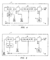
- circuit 1 includes a bias circuit 4 connected between a data output of a data source 5 and a data input of device 2A.
- Bias circuit 4 commonly referred to as a level shifter, includes a first input for receiving an input signal, such as a signal having little or no DC offset, a second input for receiving a DC bias, and an output.
- Bias circuit 4 combines the DC bias appearing at its second input to the signal appearing at the first input to obtain a combined signal, and applies the combined signal to the output of bias circuit 4. In this way, bias circuit 4 is used to vary the DC offset of the data signal applied to the device 2A.
- device 2B may internally add a DC bias to a digital signal generated by device 2B. In this instance, bias circuit 4 would be unnecessary.
- circuit 1 includes a phase shift circuit 7 connected between a system clock 11 of system 3 and the clock input of device 2A.
- Phase shift circuit 7 includes a clock input and a control input. The output signal generated by phase shift circuit 7 is shifted in phase relative to the clock input thereof by an amount based upon the control input.
- the clock skew between the input clocks for device 2B and device 2A may be set to the desired amount.
- a voltmeter 8 is connected to the output of device 2A via a splitter circuit 6. Voltmeter 8 measures and visually indicates the DC voltage appearing at the output of device 2A. Splitter circuit 6 allows voltmeter 8 to measure the DC level appearing in the output of device 2A.
- the operation of the present invention to optimize the clock skew between device 2B and device 2A in system 3 is, in general terms, a two step operation. First, the clock skew between device 2A and device 2B is adjusted to approximately 180 degrees. Second, the 180 degree clock skew is then shifted by approximately 180 degrees so as to set the clock skew between devices 2A and 2B to approximately zero degrees.
- a DC offset added to the input data pattern applied to device 2A can be used to determine when the clock skew between devices 2A and 2B is 180 degrees.
- data source 5 provides an input data pattern to device 2A having a particular duty cycle, i.e., a particular ratio of logic one data bits to logic zero data bits. If the clock skew between the clock input of device 2A and the clock input of data source 5 is optimized (i.e., at a clock skew such that input data to device 2A is interpreted without error), the output of device 2A will have the same duty cycle as the input data pattern. The DC component of the output of device 2A will therefore correspond to the particular duty cycle of the input data pattern provided to device 2A.
- device 2A will ideally make random decisions at each triggering edge of the clock input to device 2A.
- the random decisions are whether to interpret the input data pattern as the outgoing data bits (already maintained by device 2A) or the incoming data bits (appearing at the data input of device 2A).
- the duty cycle of the output data pattern generated by device 2A will ideally be the same as the duty cycle of the input data pattern applied to device 2A. From this it can be seen that for a clock skew of 180 degrees between devices 2A and 2B, the DC component of the data pattern appearing at the output of device 2A will closely correspond to the duty cycle of the input data pattern applied to device 2A.
- a DC offset in the direction of a logic zero value will increase the likelihood that logic zero data bits will be interpreted by device 2A. Most of the input data bits of the input data pattern that transition will be interpreted as a logic zero data bit. The increase in logic zero data bit interpretation decreases the duty cycle of the data output pattern generated by device 2A to approximately 0% and thereby decreases the DC component of the data output pattern generated by device 2A.
- the duty cycle of the output data pattern generated by device 2A will be between 0% and 50%.
- the resulting DC bias in the output data pattern will therefore be less in magnitude at clock skew amounts close to 180 degrees than the DC bias in the output data pattern at a 180 degree clock skew.
- clock skew amounts close to 180 degrees, the transfer of DC offset from the data input to device 2A to the data output thereof is therefore less than the transfer of DC offset at a 180 degree clock skew.
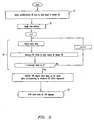
- FIG. 2 A curve illustrating the relationship between clock skew and the transfer of DC offset from the data input of device 2A to the data output thereof is shown in Fig. 2.
- the curve of Fig. 2 describes the DC offset transfer characteristic of device 2A over a range of clock skew values. It is understood that the shape of the curve of Fig. 2 may depend in part upon the characteristics of the particular hardware in system 3.
- bias circuit 4 is manipulated at 31 so that a predetermined DC offset is added to the data provided to the data input of device 2A.
- the magnitude of the predetermined DC offset is selected to be large enough so that a measurable DC offset level may be transferred from the data input of device 2A to the data output thereof, and small enough so that transferred DC offset peaks at the 180 clock skew instead of the peak being broadened so as to make the peak relatively indistinguishable.
- the data pattern is applied to device 2A at 32.
- the data pattern may be a repeated data pattern so that data is substantially continuously provided to device 2A during the operation to optimize the clock skew.
- phase shift circuit 7 in Fig. 1 provides a clock skew between the clock input to device 2A and the clock input to data source 5 (i.e., the system clock 11), phase shift circuit 7 may be located elsewhere in circuit 1 while still allowing a clock skew between device 2A and data source 5.
- Fig. 4 illustrates a circuit 10 according to another exemplary embodiment of the present invention.
- the phase shift circuit 7 of circuit 10 is disposed between the system clock 11 and the clock input to data source 5.
- the system clock 11 is in this embodiment directly connected to the clock input of device 2A.
- Circuit 10 may be employed to set the clock skew between the clock input of device 2A and the clock input of data source 5 to the optimum value.
- the operation for setting the clock skew to the optimum value is substantially the same as the operation described above with respect to circuit 1 of Fig. 1.
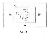
- Fig. 6 illustrates a device under test 15 having a plurality of data inputs.
- the desired clock skew between the clock input to device 15 and the clock input to the data source may be obtained by setting all but one of the data inputs to device 15 to a static or constant logic level and applying a data pattern to one data input.
- the timing of the various data sources providing data to device 15 may be adjusted to the desired or optimum setting.
- device 15 is illustrated as a multiplexer circuit for exemplary purposes only. It is understood that device 15 may be virtually any clocked, multiple-input device.
Landscapes
- Engineering & Computer Science (AREA)
- General Engineering & Computer Science (AREA)
- Physics & Mathematics (AREA)
- General Physics & Mathematics (AREA)
- Synchronisation In Digital Transmission Systems (AREA)
Claims (10)
- Procédé d'ajustement des signaux d'horloge d'un dispositif (2A) dans un système (3), comprenant :l'ajustement d'approximativement 180 degrés d'un décalage d'horloge entre une entrée d'horloge dans le dispositif (2A) et une entrée d'horloge dans une source de données (5) fournissant les données au dispositif (2A) pour obtenir un décalage d'horloge de 180 degrés ;l'ajout d'une tension de décalage continue aux données fournies par la source de données (5) ; etle déplacement d'approximativement 180 degrés du décalage d'horloge de 180 degrés.
- Procédé selon la revendication 1, dans lequel :l'étape d'ajustement comprend l'ajustement du décalage d'horloge entre le dispositif (2A) et deux quantités séparées de décalage d'horloge d'approximativement +180 degrés et -180 degrés ; etl'étape de déplacement comprend le déplacement du décalage d'horloge d'une des deux quantités séparées de décalage d'horloge à une quantité de décalage d'horloge située approximativement en un point central entre les deux quantités séparées de décalage d'horloge.
- Procédé selon la revendication 1, dans lequel l'étape d'ajustement comprend :le paramétrage initial de la tension de décalage continue d'au moins une entrée de données du dispositif (2A) à un niveau prédéterminé ;l'ajustement du décalage d'horloge entre l'entrée d'horloge dans le dispositif (2A) et l'entrée d'horloge dans la source de données (5) d'approximativement 180 degrés ;l'application d'un modèle de données à la au moins une entrée de données du dispositif (2A) ;la modification du décalage d'horloge ;la surveillance d'une sortie de données du dispositif (2A) ; etl'identification du décalage d'horloge de 180 degrés correspondant à une tension de décalage continue maximale apparaissant à la sortie du dispositif (2A).
- Procédé selon la revendication 1, dans lequel l'étape d'ajustement comprend :le paramétrage initial d'une tension de décalage continue d'au moins une entrée de données du dispositif (2A) à un niveau initial ; etla détermination d'une quantité de décalage d'horloge résultant d'une tension de décalage continue maximale dans une sortie de données du dispositif (2A), la quantité de décalage d'horloge comprenant le décalage d'horloge de 180 degrés.
- Circuit (1) destiné à ajuster des signaux d'horloge pour un dispositif (2A) dans un système (3) comprenant :un premier circuit (7 ; 9) destiné à ajuster sélectivement un décalage d'horloge entre une entrée d'horloge dans le dispositif (2A) et une entrée d'horloge dans une source de données (5) fournissant des données à une entrée de données du dispositif (2A) ;un deuxième circuit (4) connecté à une entrée de données du dispositif (2A) destiné à fournir une tension de décalage continue aux signaux apparaissant à l'entrée de données du dispositif (2A) ; etun troisième circuit (6) couplé à une sortie de données du dispositif (2A) destiné à mesurer une tension de décalage continue de la sortie de données du dispositif (2A).
- Circuit selon la revendication 5, dans lequel :le premier circuit (7 ; 9) ajuste sélectivement un retard entre l'entrée d'horloge dans le dispositif (2A) et une sortie de la source de données (5) fournissant des données au dispositif (2A).
- Circuit (1) selon la revendication 6, dans lequel :le premier circuit comprend un circuit de retard (9) présentant une première entrée connectée à une sortie de données de la source de données (5) et une sortie couplée à la première entrée du dispositif (2A) et capable de fournir un retard quelconque parmi une pluralité de retards entre un signal apparaissant à l'entrée du circuit de retard (9) et un signal apparaissant à la sortie de celui-ci.
- Circuit (1) selon la revendication 5 ou 6, dans lequel :la première entrée du dispositif (2A) est une entrée de données ; etla première sortie de la source de données (5) est une sortie de données.
- Circuit (1) selon la revendication 5, 6, 7 ou 8, dans lequel :le deuxième circuit (4) comprend un circuit capable de fournir une tension de décalage continue à la première entrée du dispositif (2A) présentant une valeur quelconque parmi une pluralité de valeurs de tension de décalage continue.
- Circuit (1) selon l'une quelconque des revendications 5 à 9, dans lequel le troisième circuit comprend :un circuit séparateur de signaux (6) présentant une entrée connectée à une sortie de données du dispositif (2A) et une sortie capable de fournir un signal représentatif d'une tension de décalage continue de la sortie de données du dispositif (2A).
Applications Claiming Priority (2)
| Application Number | Priority Date | Filing Date | Title |
|---|---|---|---|
| US967443 | 2001-09-28 | ||
| US09/967,443 US6823466B2 (en) | 2001-09-28 | 2001-09-28 | Circuit and method for adjusting the clock skew in a communications system |
Publications (3)
| Publication Number | Publication Date |
|---|---|
| EP1298443A2 EP1298443A2 (fr) | 2003-04-02 |
| EP1298443A3 EP1298443A3 (fr) | 2004-06-16 |
| EP1298443B1 true EP1298443B1 (fr) | 2005-09-21 |
Family
ID=25512800
Family Applications (1)
| Application Number | Title | Priority Date | Filing Date |
|---|---|---|---|
| EP02016652A Expired - Fee Related EP1298443B1 (fr) | 2001-09-28 | 2002-07-25 | Circuit et procédé pour ajuster le décalage d'horloge dans un système de communication |
Country Status (4)
| Country | Link |
|---|---|
| US (1) | US6823466B2 (fr) |
| EP (1) | EP1298443B1 (fr) |
| JP (1) | JP2003198521A (fr) |
| DE (1) | DE60206232T2 (fr) |
Families Citing this family (4)
| Publication number | Priority date | Publication date | Assignee | Title |
|---|---|---|---|---|
| US6823466B2 (en) * | 2001-09-28 | 2004-11-23 | Agilent Technologies, Inc. | Circuit and method for adjusting the clock skew in a communications system |
| US6973603B2 (en) * | 2002-06-28 | 2005-12-06 | Intel Corporation | Method and apparatus for optimizing timing for a multi-drop bus |
| US10632087B2 (en) | 2012-02-06 | 2020-04-28 | Innovative Med Concepts, LLC. | Famciclovir and meloxicam combination therapy for functional somatic syndromes |
| CN104243222A (zh) * | 2013-06-06 | 2014-12-24 | 鸿富锦精密工业(深圳)有限公司 | 网络设备性能测试方法及测试装置和测试系统 |
Family Cites Families (9)
| Publication number | Priority date | Publication date | Assignee | Title |
|---|---|---|---|---|
| US4550405A (en) * | 1982-12-23 | 1985-10-29 | Fairchild Camera And Instrument Corporation | Deskew circuit for automatic test equipment |
| US4546269A (en) * | 1983-12-01 | 1985-10-08 | Control Data Corporation | Method and apparatus for optimally tuning clock signals for digital computers |
| US5157277A (en) * | 1990-12-28 | 1992-10-20 | Compaq Computer Corporation | Clock buffer with adjustable delay and fixed duty cycle output |
| JPH0832425A (ja) * | 1994-07-18 | 1996-02-02 | Fujitsu Ltd | データ読み取りタイミング可変回路 |
| US5856753A (en) * | 1996-03-29 | 1999-01-05 | Cypress Semiconductor Corp. | Output circuit for 3V/5V clock chip duty cycle adjustments |
| US6108794A (en) * | 1998-02-24 | 2000-08-22 | Agilent Technologies | Signal comparison system and method for improving data analysis by determining transitions of a data signal with respect to a clock signal |
| US6239629B1 (en) * | 1999-04-29 | 2001-05-29 | Agilent Technologies, Inc. | Signal comparison system and method for detecting and correcting timing errors |
| US6687844B1 (en) * | 2000-09-28 | 2004-02-03 | Intel Corporation | Method for correcting clock duty cycle skew by adjusting a delayed clock signal according to measured differences in time intervals between phases of original clock signal |
| US6823466B2 (en) * | 2001-09-28 | 2004-11-23 | Agilent Technologies, Inc. | Circuit and method for adjusting the clock skew in a communications system |
-
2001
- 2001-09-28 US US09/967,443 patent/US6823466B2/en not_active Expired - Fee Related
-
2002
- 2002-07-25 EP EP02016652A patent/EP1298443B1/fr not_active Expired - Fee Related
- 2002-07-25 DE DE60206232T patent/DE60206232T2/de not_active Expired - Fee Related
- 2002-09-19 JP JP2002273199A patent/JP2003198521A/ja active Pending
Also Published As
| Publication number | Publication date |
|---|---|
| EP1298443A3 (fr) | 2004-06-16 |
| US20030065988A1 (en) | 2003-04-03 |
| EP1298443A2 (fr) | 2003-04-02 |
| JP2003198521A (ja) | 2003-07-11 |
| DE60206232D1 (de) | 2005-10-27 |
| DE60206232T2 (de) | 2006-06-22 |
| US6823466B2 (en) | 2004-11-23 |
Similar Documents
| Publication | Publication Date | Title |
|---|---|---|
| US8570881B2 (en) | Transmitter voltage and receiver time margining | |
| US7545190B2 (en) | Parallel multiplexing duty cycle adjustment circuit with programmable range control | |
| US7031420B1 (en) | System and method for adaptively deskewing parallel data signals relative to a clock | |
| US6834255B2 (en) | Timing control means for automatic compensation of timing uncertainties | |
| CN113841334A (zh) | 多相时钟占空比与时偏的测量和校正 | |
| US7860472B2 (en) | Receiver circuit and receiver circuit testing method | |
| US6864715B1 (en) | Windowing circuit for aligning data and clock signals | |
| US6236695B1 (en) | Output buffer with timing feedback | |
| JPH06350440A (ja) | 半導体集積回路 | |
| US6798241B1 (en) | Methods for aligning data and clock signals | |
| US6680636B1 (en) | Method and system for clock cycle measurement and delay offset | |
| US20040223566A1 (en) | Method and apparatus for skew adjustment, data transmission system having skew adjustability | |
| KR101447506B1 (ko) | 바이어스 및 랜덤 지연 소거 | |
| US6999547B2 (en) | Delay-lock-loop with improved accuracy and range | |
| US6735732B2 (en) | Clock adjusting method and circuit device | |
| EP3980860B1 (fr) | Circuits et procédés d'étalonnage d'un circuit dans un dispositif de circuit intégré | |
| CN114556784A (zh) | 正交时钟偏斜校准电路 | |
| TW567675B (en) | Digitally controlled pulse width adjusting circuit | |
| EP1298443B1 (fr) | Circuit et procédé pour ajuster le décalage d'horloge dans un système de communication | |
| KR20040082376A (ko) | 위상 조정 장치 및 반도체 시험 장치 | |
| WO2002039629A9 (fr) | Systeme de calibrage de temps de voie | |
| US7197053B1 (en) | Serializer with programmable delay elements | |
| US7092471B2 (en) | Digital phase synchronization circuit | |
| GB2375274A (en) | Receiver with automatic skew compensation | |
| US8139697B2 (en) | Sampling method and data recovery circuit using the same |
Legal Events
| Date | Code | Title | Description |
|---|---|---|---|
| PUAI | Public reference made under article 153(3) epc to a published international application that has entered the european phase |
Free format text: ORIGINAL CODE: 0009012 |
|
| AK | Designated contracting states |
Designated state(s): AT BE BG CH CY CZ DE DK EE ES FI FR GB GR IE IT LI LU MC NL PT SE SK TR Kind code of ref document: A2 Designated state(s): AT BE BG CH CY CZ DE DK EE ES FI FR GB GR IE IT LI LU MC NL PT SE SK TR |
|
| AX | Request for extension of the european patent |
Extension state: AL LT LV MK RO SI |
|
| PUAL | Search report despatched |
Free format text: ORIGINAL CODE: 0009013 |
|
| AK | Designated contracting states |
Kind code of ref document: A3 Designated state(s): AT BE BG CH CY CZ DE DK EE ES FI FR GB GR IE IT LI LU MC NL PT SE SK TR |
|
| AX | Request for extension of the european patent |
Extension state: AL LT LV MK RO SI |
|
| 17P | Request for examination filed |
Effective date: 20040708 |
|
| 17Q | First examination report despatched |
Effective date: 20040812 |
|
| AKX | Designation fees paid |
Designated state(s): DE GB |
|
| GRAP | Despatch of communication of intention to grant a patent |
Free format text: ORIGINAL CODE: EPIDOSNIGR1 |
|
| GRAS | Grant fee paid |
Free format text: ORIGINAL CODE: EPIDOSNIGR3 |
|
| GRAA | (expected) grant |
Free format text: ORIGINAL CODE: 0009210 |
|
| AK | Designated contracting states |
Kind code of ref document: B1 Designated state(s): DE GB |
|
| REG | Reference to a national code |
Ref country code: GB Ref legal event code: FG4D |
|
| RIN1 | Information on inventor provided before grant (corrected) |
Inventor name: KARLQUIST, RICHARD K. |
|
| REF | Corresponds to: |
Ref document number: 60206232 Country of ref document: DE Date of ref document: 20051027 Kind code of ref document: P |
|
| PLBE | No opposition filed within time limit |
Free format text: ORIGINAL CODE: 0009261 |
|
| STAA | Information on the status of an ep patent application or granted ep patent |
Free format text: STATUS: NO OPPOSITION FILED WITHIN TIME LIMIT |
|
| 26N | No opposition filed |
Effective date: 20060622 |
|
| PGFP | Annual fee paid to national office [announced via postgrant information from national office to epo] |
Ref country code: DE Payment date: 20070831 Year of fee payment: 6 |
|
| PGFP | Annual fee paid to national office [announced via postgrant information from national office to epo] |
Ref country code: GB Payment date: 20070727 Year of fee payment: 6 |
|
| GBPC | Gb: european patent ceased through non-payment of renewal fee |
Effective date: 20080725 |
|
| PG25 | Lapsed in a contracting state [announced via postgrant information from national office to epo] |
Ref country code: DE Free format text: LAPSE BECAUSE OF NON-PAYMENT OF DUE FEES Effective date: 20090203 |
|
| PG25 | Lapsed in a contracting state [announced via postgrant information from national office to epo] |
Ref country code: GB Free format text: LAPSE BECAUSE OF NON-PAYMENT OF DUE FEES Effective date: 20080725 |